
Submitted:
04 May 2023
Posted:
05 May 2023
You are already at the latest version
Abstract
The successful handling of large semiconductor wafers is crucial for scaling up their production. Early-stage warpage control allows to prevent undesirable asymmetric warpage, known as wafer bifurcation or buckling. Indeed, even in a gravity-free environment, thinning an 8" or 12" semiconductor wafer can result in warpage and bifurcation. To mitigate this issue, the taiko method, which involves creating a thicker ring region around the rim of the wafer, has been widely used. Previous research has focused on the theoretical factors affecting the warpage of a backside metalized taiko wafer. This work extends the case to a front-side metalized taiko wafer and introduces the concept of the equivalent thickness of a taiko wafer. The equivalent thickness of a taiko wafer, influenced by the ring region, lies in between the thickness of the central region and that of the annular region. Because of the limited number of taiko wafers that can be produced on a production line, modelling can be beneficial. In this work we compared the results of a developed analytical model with those obtained from a finite element analysis (FEA) approach with ANSYSY® software to model the equivalent thickness of a taiko wafer. We investigated the curvature as a function of the stress of the metal layer, considering key design factors such as the substrate region thickness, the thickness of the thin metal film, the step height, and the width of the ring region. By systematically varying the thickness of the central region of the taiko wafer, we explored the curvature as a function of stress induced by thermal load in the linear regime and determined the slopes in the linear region of the curvature vs. stress curves. The aim of this study is to identify regularities and similarities with the Stoney equation and investigate the validity of the analytical approach for the case of a taiko substrate. It results that there is a good agreement between the analytical model of a taiko wafer and the numerical analysis gained by the FEA methods.
Keywords:
Taiko Wafers
; Finite Elements Analysis (FEA)
; ANSYS thermomechanical simulations
1. Introduction
Vertical power MOSFETs based on silicon [1] and silicon carbide [2] devices, intended for the automotive sector, need a considerable cutdown of the switching losses and Joule heating effect [3,4]. A method to achieve this consists in reducing the thickness of the semiconductor wafer. However, the combined effect of a thinned substrate along with e.g., a front side metallization (FSM) determines a severe warpage of the whole wafer, which can hinder the performances and the subsequent manufacturing processes needed to complete the devices.
Containing the warpage of the wafer determined by the FSM residual stress is crucial in the semiconductor industry. Indeed, the handling of the wafer as the size increases can be an issue, also in the case of SiC substrates [5,6]. A method to solve the issue involves the use of taiko wafers [7,8,9], which consists of back-grinded wafers having a ring region of the wafer which is preserved. It results that, because of the intrinsic structure of the taiko wafer, for a given metal stress and metal film thickness, the resulting warpage of a FSM-thinned wafer is mitigated with respect to the case of a canonical or flat metallized thinned wafer.
To gain an analytical description of the system, we start from the simplification of a disk-shaped wafer. A thin FSM metal film, deposited on the front side of a semiconductor wafer, warps the whole metalized wafer until the net forces and the resulting bending moments zero-condition is reached. From this it is possible to gain an estimate of the resulting curvature. If the substrate thickness is constant and negligible with respect to the diameter of the wafer, by considering a thickness of the film, uniform and small compared to that of the substrate, an average film stress, can be determined from the curvature of the elastically deformed coated substrate, according to the Stoney’s formula [10,11]. The Stoney equation can be written be written as:
where the biaxial modulus is also considered. Equation (1.1) provides a direct linear relationship between the measured average curvature and the average film stress . In the equation , and are the Young modulus and Poisson ratio of the substrate, respectively.
In general, the Stoney equation is appropriate in the linear regime where both the residual stress and the resulting curvature are low. However, as the stress increases, deviations from linearity are observed and the curvature for a given stress of the film becomes lower than what is predicted by Equation (1.1). Corrections to the Stoney equation have been considered in the past. For example, a cubic polynomial correction to the linear dependence, has been proposed [12].
Additionally, an effort to extend Stoney's formula for non-uniform wafer thickness has been made in [13] for the case of wafers with a slight thickness change in the peripheral region. However, this work only considers the step as a small disturbance compared to the overall wafer thickness, thus it does not offer a comprehensive solution for the case of a taiko wafer.
Approaches based on Finite Element Analysis (FEA) have also been considered for the case of flat substrates using standard structural analysis tools such as ANSYS [14,15,16] and ABAQUS [17]. These works highlight that it is challenging to accurately predict the final shape of the warped flat substrate. Indeed, the numerical and stable solution is often not the physical one unless a small perturbation, which would result in a bifurcation, is applied. As far as we are aware, there have been few comprehensive studies on the general case of taiko wafers. The way the warpage changes for these wafers is therefore unclear. In this study, we offer an analytical explanation derived from the theory of elasticity to comprehend the resulting warpage in a FSM-taiko wafer. Indeed, in 2021, Vinciguerra and Landi [18] introduced an analytical method to model the bifurcation in back-side metalized taiko wafers. The following years, with Malgioglio, they reported on their investigation of the bifurcation phenomenon in 8" metalized wafers [19,20,21,22,23] by means of FEA methods and extended the investigation to understand the correlation between warpage wafer and warpage die [24]. The aim of this work is to compare the analytical description of the warpage occurring in a FSM-taiko wafer with the results obtained by Finite Element Simulations of the same system achieved by means of ANSYS® mechanical solver.
As a fact, the Stoney equation is not valid for the case of a taiko wafer since we have to consider the presence of the ring. In the current study we aim to expand the analysis of warpage to the case of a taiko wafer that has been metalized on the front side. Specifically, we aim to investigate the warpage of a front side metal (FSM) taiko wafer in the spherical regime and determine the value of the equivalent thickness for a FSM-taiko wafers.
The equivalent thickness concept in the context of a taiko wafer involves making modifications to the mathematical equation 1.1, to account for the effects of the wafer's physical properties and determine the influence of the ring region on its warpage. This includes considering the wafer as an idealized structure with a constant curvature, despite the presence of a damaged layer due to back-grinding [25].
A proposal for a modified Stoney formula for a taiko wafer can be written as:
where is the bending moment determined by the FSM and is the flexural rigidity of the FSM-taiko wafer. A rigorous determination of the values for these quantities, involves the use of the theory of elasticity [26,27].
In Figure 1 the schematic of half of the vertical cross-section of a FSM-taiko wafer is reported. A reference frame is fixed at the centre of the taiko wafer, with the origin placed on the neutral plane, such that the back side of the wafer is at with respect to the neutral plane. In the schematic, is thickness of the substrate, the height of the ring region, the internal radius and the external radius, respectively. On the front side of the wafers a thin film, e.g. metal, having a modulus of elasticity and thickness , is indicated in yellow. The neutral axis results from the intersection of the neutral plane and the cross-section plane. Once the reference is fixed, is the distance between the neutral axis (plane) and the interface substrate/thin film, is the distance between the neutral axis and the FSM thin film top-surface, whereas is the distance of the ring region surface of the taiko wafer with respect to the neutral axis. The height of the step is given by and usually is a fixed quantity.
1. Warpage of a FSM Taiko Wafer According to the Theory of Elasticity in the Spherical Case
In analogy to what reported in [18] we can develop an approximation of the warpage of a front side metalized taiko wafer. Indeed, according to the theory of elasticity, see Landau-Lifshitz, [26], if the taiko wafer is not subject to the force of gravity, the vertical displacement with respect to the neutral surface satisfies the biharmonic equation , which is valid in the ring region as well as in the thinned wafer region.
For a FSM taiko wafer as well, the biharmonic equation has the Michell’s solution [28]. However, in the spherical case, as a first approximation, the warpage can be characterized by one curvature in the substrate region and one curvature in the ring region. In detail, in the ring region, , the simplest solution does not consider the dependence on the angle and can be written as:
In the internal and thinned substrate region, , the spherical solution of the biharmonic equation is
The curvatures , and the parameters , b, c and d can be determined from the boundary conditions and .
At the interface between the FSM thin film and the wafer substrate, at a distance from the center, the taiko wafer is subject to a radial and a circumferential force, whose values per unit length are set equal to and , respectively (See Figure 1).
The wafer is considered supported at the external ring , and and are the reaction forces evaluated per unit length (See Figure 1).
Because of the mechanical equilibrium, the resultant of the forces and the moments must be equal to zero. In particular, the equilibrium of forces and moments holds locally for the thin film deposited in the substrate region:
And the reaction moments acting on the ring at are in equilibrium with those of the substrate.
By reasoning similarly to the case of ref [18], the moments per unit length in the substrate region and ring region can be written as:
Where and are the flexural rigidity of the substrate and ring regions, respectively. Whereas and are the moments of inertia of a section of the taiko wafer, considered as a beam of width , with respect to the neutral axis [29], in the substrate and ring region, respectively.
Being the forces per unit length acting on the length , the moment equals .
Since , and , in the limit , , which implies that . Moreover, in the limit , , and according to the Stoney formula , which implies that . Hence, the set of four equations for the moments can be written as:
In general, and are functions of , such that in the limit , .
The equation
is the extension of the Stoney formula for the case of a FSM taiko wafer. It can be solved once that and are known.
2. Determination of the moment of inertia
By following reference [30] along with the schematic of Figure 1, it is possible to gain an expression of the flexural rigidities and. Indeed, the total bending moment per unit length acting in the substrate region coated with the FSM film can be expressed as:
Hence, the flexural rigidity of the substrate region, corrected by the Poisson coefficients of the thin film and of the substrate is:
If , . In the limit , since , becomes , which is what we expect.
Analogously, in the ring region it holds:
and the flexural rigidity in this region becomes,
4. Evaluation of
To gain the mechanical stress of the thin metal film, from measurement of warpage, we need to evaluate . This quantity can be calculated from the equilibrium of the forces.
In the substrate region. By following still [30] we can write the total force acting in the substrate region in the radial direction as:
where and .
At a given distance we can write,
and the total force acting on the substrate region is
being .
In the ring region. In the ring region we need to evaluate the quantity:
The case of the taiko wafer. Hence, the total force acting on the taiko wafer, in the radial direction, equals zero, being in equilibrium:
In the limit , , Equation (4.6) reduces to the canonical case of a flat disk wafer:
where is equal to
which is the value of the limit if . Moreover, if , .
To evaluate in the general case, it is necessary to combine, the modified Stoney formula for the taiko wafer (Equation (2.7)) and calculate the value of the integral (see Appendix B of ref [18] according to the function evaluated in Appendix A in the same ref [18]. By doing so a linear equation is obtained, whose solution provides the value of the neutral axis
Where is the normalized function reported in Equation (A1) of Appendix A of ref (on the way).
By developing the calculations, we have that the neutral plane is given by:
If , this expression is simplified as
The normalized integral
has been evaluated and its value is also reported in Appendix B of Ref. [18].
By substituting the value of in Equation (2.7) we obtain that the curvature can be expressed as:
By considering the Stoney approximation in Equation (1.1), we can express a new quantity, defined as the equivalent thickness of a FSM taiko wafer, which is the thickness that a plain wafer should have to determine the same slope in the curvature-stress curve . The equivalent thickness of a taiko wafer can hence be determined from Equation (4.14):
and expressed as
In the specific case of Equation (4.13), the equivalent thickness of a taiko wafer depends on as
As in the case reported in ref [18], besides the equilibrium of the forces in the radial direction, also the net forces along the circumferential direction must be considered. In the case of a FSM-taiko wafer, the net forces in direction must satisfy equation:
which leads to an additional value of the
that can be simplified, if , as
Also, in this case the normalized integral
has been evaluated and reported in appendix B of ref [18].
In the event, it results that it is possible to calculate and additional value of , which determine the curvature
And hence an additional value of the slope .
To summarize, it results that there are two values of , a value determined by Equation (4.13), hereafter indicated as , which determines a neutral axis along the radial direction, because of the radial net force, and a value determined by Equation (4.21), hereafter indicated with , which determines an additional neutral axis in the radial direction determined by the equilibrium of the net circumferential forces.

Table 2.
Values of the Integral I1 and I2.
| (mm) | Width (mm) | (mm) | (µm) | Young Modulus (GPa) | |||
|---|---|---|---|---|---|---|---|
| 100 | 3.7 | 96.3 | 450 | 0.27 | 130 | -1.5894 | 5.5181 |
6. ANSYS Finite Element Model of a FSM-Taiko Wafer in the Spherical Case
Along with the analytical approach reported in the previous section, an investigation of the FSM-taiko wafer has been carried out by realizing finite element method (FEM) simulations with the software tool ANSYS® Mechanical Enterprise 2022/R2. The geometry of the system is the same as the one reported in Figure 1a. The mechanical behaviour of a system consisting of a 200 mm (8”) taiko silicon wafer, coated with a 4.5 μm Al metal layer on the front side, has been simulated in the spherical case.
The simulations conditions were the following. Mesh preferences were set as non-linear mechanical. A regular radial mesh was optimized by dividing the geometry model of the Silicon wafer and Al layer into 12 parts resulting from the intersections of three concentric rings with four quadrants, for a total of 24 parts, by considering both the silicon substrate and the aluminium layer. Moreover, the taiko wafer was laid on four supports, symmetrically positioned at the edge. Each support consists of an elastic facet having dimensions of 4 mm x3 mm, whose foundation stiffness was set equal to 1 N/mm3. The face-to-face contacts between the silicon and aluminium layers was set as bonded. In the FEM analysis the physics chosen was the Static Structural. A direct solver type was used by setting the large deflection on, and the weak springs condition has been settled on. In Figure 2a,b a snapshot of the top plan-view and rear plan-view of the simulated taiko wafer film, with the ring region and the four supports highlighted, is shown.
The silicon substrate (001) has been simulated by taking into account of its elastic constants opportunely chosen accordingly to the face orientation such that to reproduce a Young’s modulus of ESi=130 GPa and Poisson’s ratio and νSi=0.27, respectively. The Al layer has been considered as an isotropic material, with a Young modulus of EAl =68 GPa and νAl = 0.33, respectively. The coefficients of thermal expansion (CTEs) of silicon and aluminum have been gained from a set of values tabulated at specific temperatures and then interpolated for intermediate values. For each simulation a thermal load was applied to the whole system, by considering the stress-free condition at the higher nominal temperature T. The FSM-taiko wafer was cooled down from the nominal temperature T in °C to the temperature of 25°C. Temperatures ranging from 30°C up to 170 °C have been simulated.
7. ANSYS Results
For a given nominal temperature T, the warpage of the taiko wafer was probed by determining the directional deformation along the z direction of the whole system, as well on a set of three pairs of paths extending along the diameter of the wafer. Each pair of the three was oriented according to two perpendicular directions, the x and y direction of the coordinate system. Of the three pairs, the first pair of paths was set at the base of the taiko wafer, the second pair of paths at the interface between the Si substrate and the Al layer and the third pairs at the top of the Al layer. The value of the warpage was recorded for each nominal temperature and the curvature calculated. In Figure 3a we report the distribution of the directional deformation along the z direction for a taiko wafer 200 µm thin, simulated at a nominal temperature of T=50°C. All the other quantities have been set to the typical values. In Figure 3b we report the projection of the distribution of the directional deformation along the z direction for the same taiko wafer 200 µm thin, simulated at a nominal temperature of T=50°C. The magnification is 100 x. In Figure 4 from a to f we report the indication of the three pairs of x- and y- paths for this specific case.
In Figure 5 we report the directional deformation along the z direction for each pair of paths 1x, 1y, on the top of the metal layer, 2x, 2y, at the interface between the metal layer and the semiconductor, 3x and 3y, at the bottom of the central taiko semiconductor region, respectively, reported as a function of the coordinate x (y) along the path itself, for the case of FSM-taiko wafer 200µm thin. In general, we observed that for each pair of paths there isn’t any difference in the curvatures in the x- and y- directions, confirming that the wafer has warped symmetrically. Moreover, all the paths provide the same deformation. The curvature at the centre of the wafer has been determined from a parabolic approximation and the trend according to the theory reported for a comparison. We can observe as the parabolic trend fits well with the directional deformation of the taiko wafer.
In Figure 6 the curvature as a function of the stress for a taiko wafer having hs =200 µm and the other quantities fixed to the typical value reported in Table 1 has been reported. In the graph, it is reported the line determined by the slope of the Stoney equation and the tangent line to the curvature vs Stress curve. The slope, defined by the ration and hence the curvature for the taiko wafer is lower with respect to the Stoney case.
In Figure 7 we report the curvature as a function of the stress for a set of seven taiko wafers having hs ranging in the interval 100 - 400 µm and the other quantities fixed to the typical value reported in Table 1. In particular, the height was set to a constant value of 450 µm. For each , we calculated the slope of the tangent line to the origin of the curve.
In Figure 8, the values of these slopes () have been reported as a function of the thickness of the substrate in the central region of the taiko wafer. For comparison, we reported also the slope determined by the Stoney equation for a flat wafer. As can be observed, the slope, and hence the curvature as a function of the stress, though increasing with the decrease of the thickness of the wafer, is lower with respect to the case of a flat substrate or Stoney case, because of the mitigation effect determined by the taiko wafer. To complete our investigation on the FSM-taiko wafer we calculated the slope as a function of the thickness as provided by the analytical developments reported in the first part of this work, by Equations (4.13) and (4.21). The results have been compared with those provided by ANSYS and reported in the same Figure 8. It results that the values of the slopes are practically the same, that is there’s one value for the zB value. Moreover, though the calculated values are well below the value provided by ANSYS, it is possible to gain the order of magnitude of the slope and the same trend. Finally, it is worth to observe that by adding the two contributions of the slopes and , determined by the developed theory, we found a good agreement with the ANSYS the simulation experiment. This indicated that the theory explains well the physics which is behind the mitigation of the warpage of a taiko wafer.
Lastly, in Figure 9, we report the equivalent thickness calculated according to Equation (4.15), of the wafer as calculated from the theory and from the ANSYS results as a function of hs. It results as the FSM taiko wafer warps as an equivalent wafer having a higher thickness of the substrate.
Conclusions
In conclusion the equivalent thickness of a front side metallized taiko wafer has been determined theoretically and measured by means of finite element analysis methods. A comparison of the two approach reveals that the analytical solution grasps the order of magnitude and the trend of the mitigation of the curvature due to the structure of the taiko wafer. The FSM-taiko wafer behaves as an equivalent flat wafer whose thickness is higher than the substrate thickness. The obtained results can be extended also to other wide band gap semiconductors such as silicon carbide and gallium nitride.
Author Contributions
V.V. Conceptualization of the work, Analytical model elaboration, conceptualization of the ANSYS® simulations experiment, data elaboration, paper drafting, editing and writing. G.L.M. ANSYS® system design, optimization and simulations. A.L. first validation of the approach, M.R. sponsorship, funding, validation. All Authors revised the paper and approved the final version.
References
- J. Lutz, H. Schlangenotto, U. Scheuermann and R. De Doncker, “Semiconductor power devices: Physics, characteristics, reliability,” Springer International Publishing, pp. pp. 1-714., (2018).
- T. Kimoto and J. A. Cooper, Fundamentals of Silicon Carbide Technology: Growth, Characterization, Devices and Applications, John Wiley & Sons, 2014.
- V. Benda, “Power semiconductors – state of art and future trends,” AIP Conference Proceedings, pp. vol. 1337, no. 1, pp. 16–24., (2011).
- P. Fiorenza, F. Giannazzo and F. Roccaforte, "Characterization of SiO2/4H-SiC interfaces in 4H-SiC MOSFETs: A review," Energies, pp. v.12, (2019) pp. 2310., (2019).
- A. A. Messina, A. Imbruglia, M. Calabretta, V. Vinciguerra, C. C. Moise, A. Sitta, M. Enachescu and F. Roccaforte, “The "first and euRopEAn siC eighT Inches pilOt liNe": A project, called REACTION, that will boost key SiC Technologies upgrading (developments) in Europe, unleashing Applications in the Automotive Power Electronics Sector,” in 2020 AEIT International Conference of Electrical and Electronic Technologies for Automotive, AEIT AUTOMOTIVE 2020, 2020.
- “REACTION JU ECSEL,” [Online]. Available: https://www.ecsel.eu/projects/reaction.
- S. Yoshida and O. Nagai, "Wafer Grinding Method". Patent United States Patent US7462094B2, 2008.
- [Online]. Available: http://www.disco.co.jp/eg/solution/library/taiko.html, .
- A. Dhadda, R. Montgomery, P. Jones, J. Heirene, R. Kuthakis and F. Bieck, “Processing of ultrathin wafers for power chip applications,” in Proceedings of the 2012 IEEE 14th Electronics Packaging Technology Conference, EPTC 2012, (2012), 2012.
- G. G. Stoney, “The tension of metallic films deposited by electrolysis,” Proceedings of the Royal Society of London. Series A, Containing Papers of a Mathematical and Physical Character, vol. 82, no. 553, 1909. [CrossRef]
- G. C. A. M. Janssen, M. M. Abdalla, F. van Keulen, B. R. Pujada and B. van Venrooy, "Celebrating the 100th anniversary of the Stoney equation for film stress: Developments from polycrystalline steel strips to single crystal silicon wafers," Thin Solid Films, vol. 517, pp. 1858-1867, 2009. [CrossRef]
- L. Freund, J. A. Flora and E. Chason., “Extensions of the Stoney formula for substrate curvature to configurations with thin substrates or large deformations,” Applied Physics Letters, vol. 74, no. 14, p. 1987, 1999. [CrossRef]
- X. Feng, Y. Huang and A. J. Rosakis, "On the stoney formula for a thin film/substrate system with nonuniform substrate thickness," Journal of Applied Mechanics, Transactions ASME, pp. v. 74, no. 6], (2007).
- A. Mallik, R. Stout and J. J. Ackaert, "Finite-element simulation of different kinds of wafer warpages: Spherical, cylindrical, and saddle," IEEE Transactions on Components, Packaging and Manufacturing Technology, vol. 4, no. 2, 2014.
- A. Mallik and R. Stout, “Simulation of process-stress induced warpage of silicon wafers using ANSYS® finite element analysis,” in 43rd International Symposium on Microelectronics 2010 IMAPS, vol. 2010, no. 1, 2010. [CrossRef]
- J. Schicker, W. Khan, T. Arnold and C. Hirschl, "Simulating the warping of thin coated Si wafers using Ansys layered shell elements," Composite Structures, no. 140, 2016. [CrossRef]
- A. H. Abdelnaby, G. P. Potirniche, F. Barlow, A. Elshabini, S. Groothuis and R. Parker, "Numerical simulation of silicon wafer warpage due to thin film residual stresses," in IEEE Workshop on Microelectronics and Electron Devices, (WMED), pp. 9-12, 2013.
- V. Vinciguerra and A. Landi, "On the Way to understand the Warpage in 8” Taiko Semiconductor Wafers for Power Electronics Applications (Si and SiC)," in 2021 22nd International Conference on Thermal, Mechanical and Multi-Physics Simulation and Experiments in Microelectronics and Microsystems (EuroSimE), St. Julian, Malta, 2021.
- V. Vinciguerra, G. L. Malgioglio and A. Landi, “Modelling the Elastic Energy of a Bifurcated Wafer: A Benchmark of the Analytical Solution vs. The ANSYS Finite Element Analysis,” Composite Structures, vol. 281, p. 114996, 2022.
- V. Vinciguerra, G. L. Malgioglio and A. Landi, "Models of Bifurcation in a Semiconductor Wafer: A Comparison of the Analytical Solution vs.The ANSYS Finite Element Analysis," 2022 23rd International Conference on Thermal, Mechanical and Multi-Physics Simulation and Experiments in Microelectronics and Microsystems, EuroSimE 2022, 2022.
- V. Vinciguerra, A. Landi and G. L. Malgioglio, "Wafer Bifurcation as a Spontaneous Symmetry Breaking," in 23rd International Conference on Thermal, Mechanical and Multi-Physics Simulation and Experiments in Microelectronics and Microsystems (EuroSimE), Malta, 2022.
- V. Vinciguerra, G. L. Malgioglio, A. Landi and M. Renna, "Models of Bifurcation and Gravity Induced Deflection in Wide Band Gap 4H-SiC Semiconductor Wafers," in 4th International Conference on Thermal, Mechanical and Multi-Physics Simulation and Experiments in Microelectronics and Microsystems (EuroSimE), Graz, Austria, 2023.
- V. Vinciguerra, M. Boutaleb, G. L. Malgioglio, A. Landi, F. Roqueta and M. Renna, "Investigating the Occurrence of Bifurcation in Large Metalized Wafers using ANSYS Layered Shell Elements," in 2023 24th International Conference on Thermal, Mechanical and Multi-Physics Simulation and Experiments in Microelectronics and Microsystems (EuroSimE), Graz, Austria, 2023.
- V. Vinciguerra, G. L. Malgioglio, A. Landi, S. Valastro, B. Cafra and M. Renna, "From Wafer Bifurcation to Warpage Die: A Correlation Method to determine the Warpage of a Metal-Coated Silicon Substrate," 2022 23rd International Conference on Thermal, Mechanical and Multi-Physics Simulation and Experiments in Microelectronics and Micro," St Julian, Malta, 2022.
- S. Gao, Z. Dong, R. Kang, B. Zhang and D. Guo, “Warping of silicon wafers subjected to back-grinding process,” Precision Engineering, vol. 40, pp. 87-93, 2015. [CrossRef]
- L. D. Landau, E. M. Lifshitz, A. M. Kosevich and L. P. Pitaevskii, Theory of Elasticity: Vol. 7 of Course of Theoretical Physics, Oxford, New York, Toronto: Pergamon Press, 1960.
- S. Timoshenko and J. Goodier, Theory of elasticity, New York: McGraw-Hill, 1970.
- J. H. Michell M.A., “On the direct determination of stress in an elastic solid, with application to the theory of plates,” in Proceedings of the London Mathematical Society, London, 1899.
- W. Young, R. Budynas and A. Sadegh, Roark's formulas for stress and strain, New York: McGraw-Hill, 2011.
- J. W. Eischen and J. S. Everett, “Thermal stress analysis of a bimaterial strip subject to an axial temperature gradient,” Journal of Electronic Packaging, Transactions of the ASME, vol. 111, no. 4, pp. 282-288, 1989. [CrossRef]
Figure 1.
Cross section of a front side metal (FSM) taiko wafer illustrating the quantities determining the warpage of the FSM taiko wafer. is the internal radius, external radius thickness of the substrate and the height of the ring. The FSM taiko wafer is subject to a radial force at the internal step edge of the ring, whose value per unit length is Fr. The wafer is supported at the external ring and Nr is the reaction force evaluated per unit length. The front of the wafer is at with respect to the neutral plane. The step height is fixed and equal to .
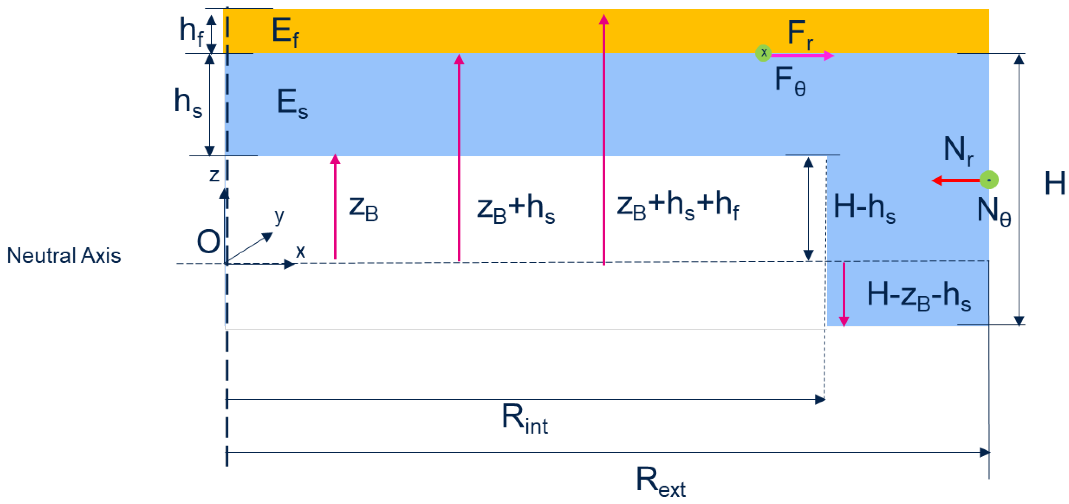
Figure 2.
(a) Top plan-view of the simulated taiko wafer and of the used mesh for the simulation. (b) Rear plan-view of the simulated taiko wafer. The ring region and the four pins are highlighted.
Figure 2.
(a) Top plan-view of the simulated taiko wafer and of the used mesh for the simulation. (b) Rear plan-view of the simulated taiko wafer. The ring region and the four pins are highlighted.
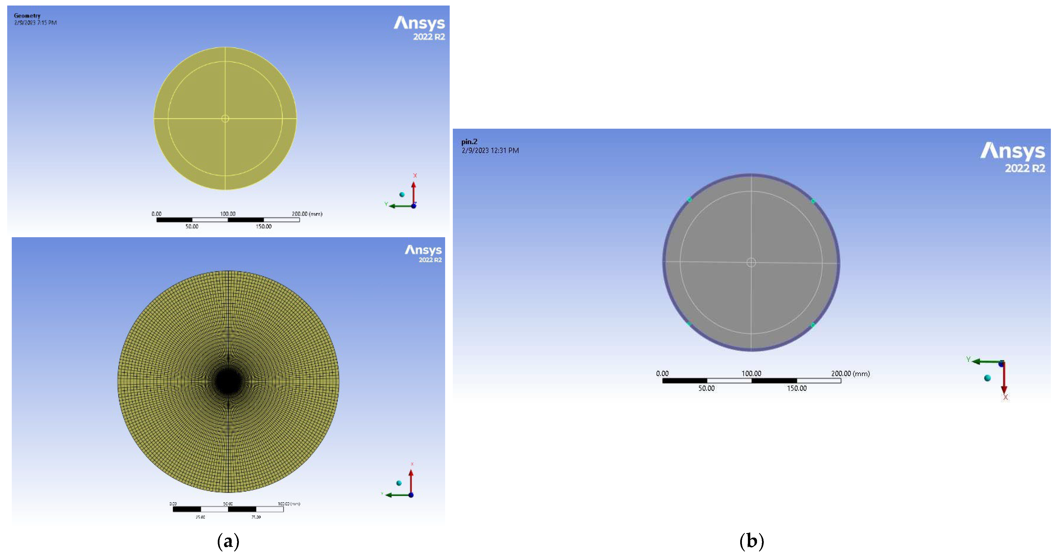
Figure 3.
(a) Distribution of the directional deformation along the z direction for a taiko wafer 200 µm thin, simulated at a nominal temperature of T=50°C. (b) Projection of the distribution of the directional deformation along the z direction for a taiko wafer 200 µm thin, simulated at a nominal temperature of T=50°C, the magnification is 100 x.
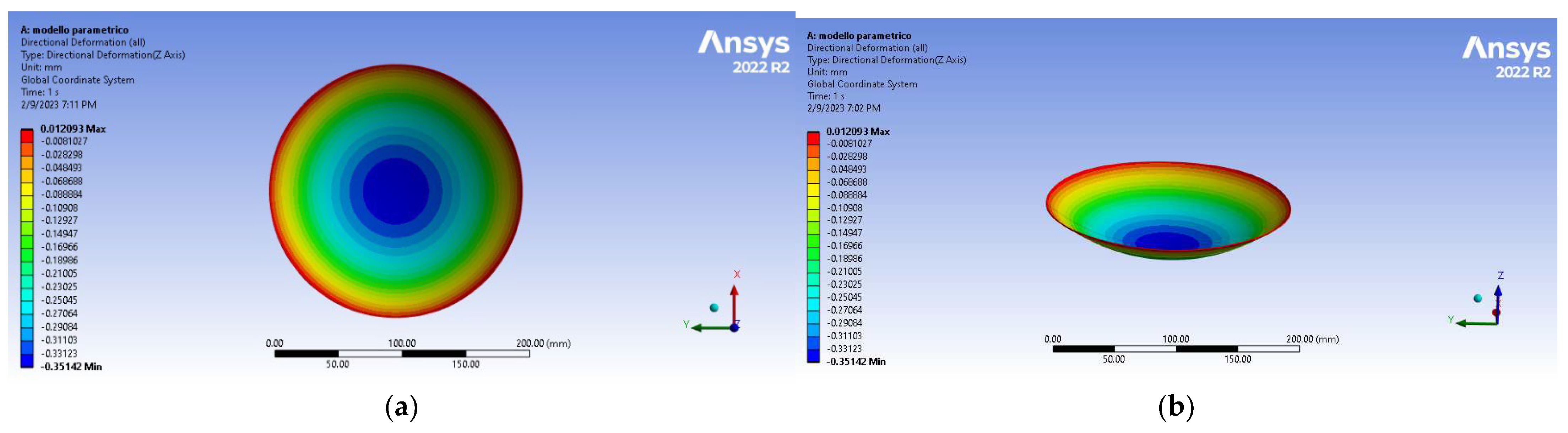
Figure 4.
(a) Snapshot of the first path used to probe the z_deformation along x direction, on the top of the Al layer. (b) Snapshot of the first path used to probe the z_deformation along y direction, on the top of the Al layer. (c) Snapshot of the 2nd path used to probe the z_deformation along x direction, at the interface of the Al/Si layers. (d) Snapshot of the 2nd path used to probe the z_deformation along y direction, at the interface of the Al/Si layers. (e) Snapshot of the 3rd path used to probe the z_deformation along x direction, at the bottom of the central substrate region of the taiko wafer. (f) Snapshot of the 3rd path used to probe the z_deformation along y direction, at the bottom of the central substrate region of the taiko wafer.
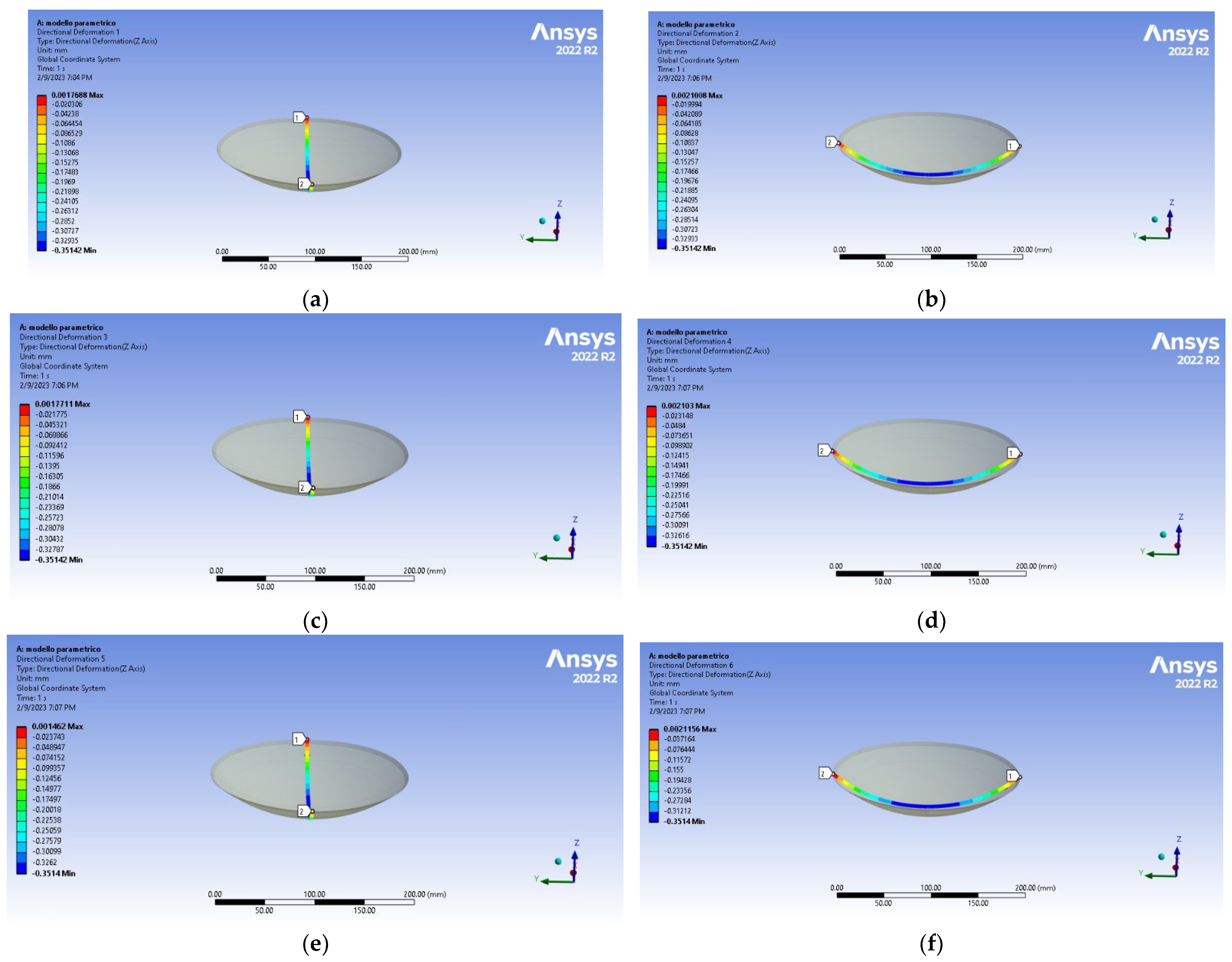
Figure 5.
Directional deformation along the z direction for each pair of paths in the x and y directions, respectively at the top of the Al metal layer, at the Si/Al interface and at the bottom of the central Si substrate of the taiko wafer, reported as a function of the coordinate x (y) along the path, for the case of FSM-taiko wafer 200µm thin. All the paths provide the same deformation. The curvature has been determined from a parabolic approximation and the trend according to the theory reported for comparison.
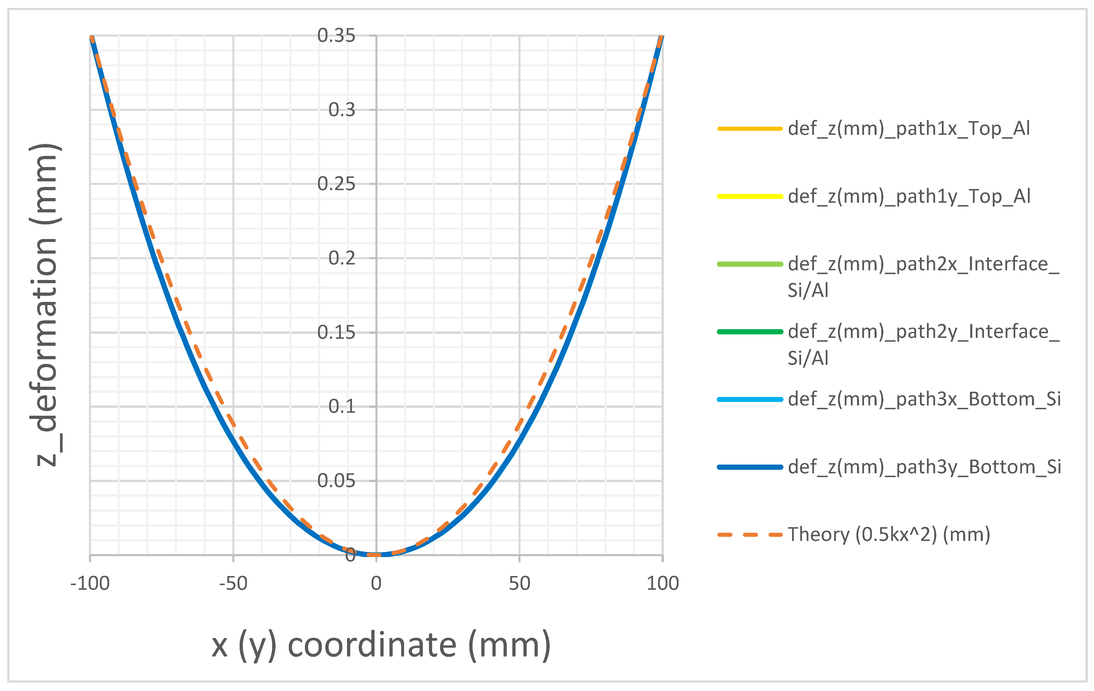
Figure 6.
Curvature as a function of the stress for a taiko wafer having hs =200 µm and the other quantities fixed to the typical value reported in Table 1. In the graph, it is reported the line determined by the slope of the Stoney equation and the tangent line to the Curvature vs. Stress curve. The slope and hence the curvature for the taiko wafer is lower with respect to the Stoney case.
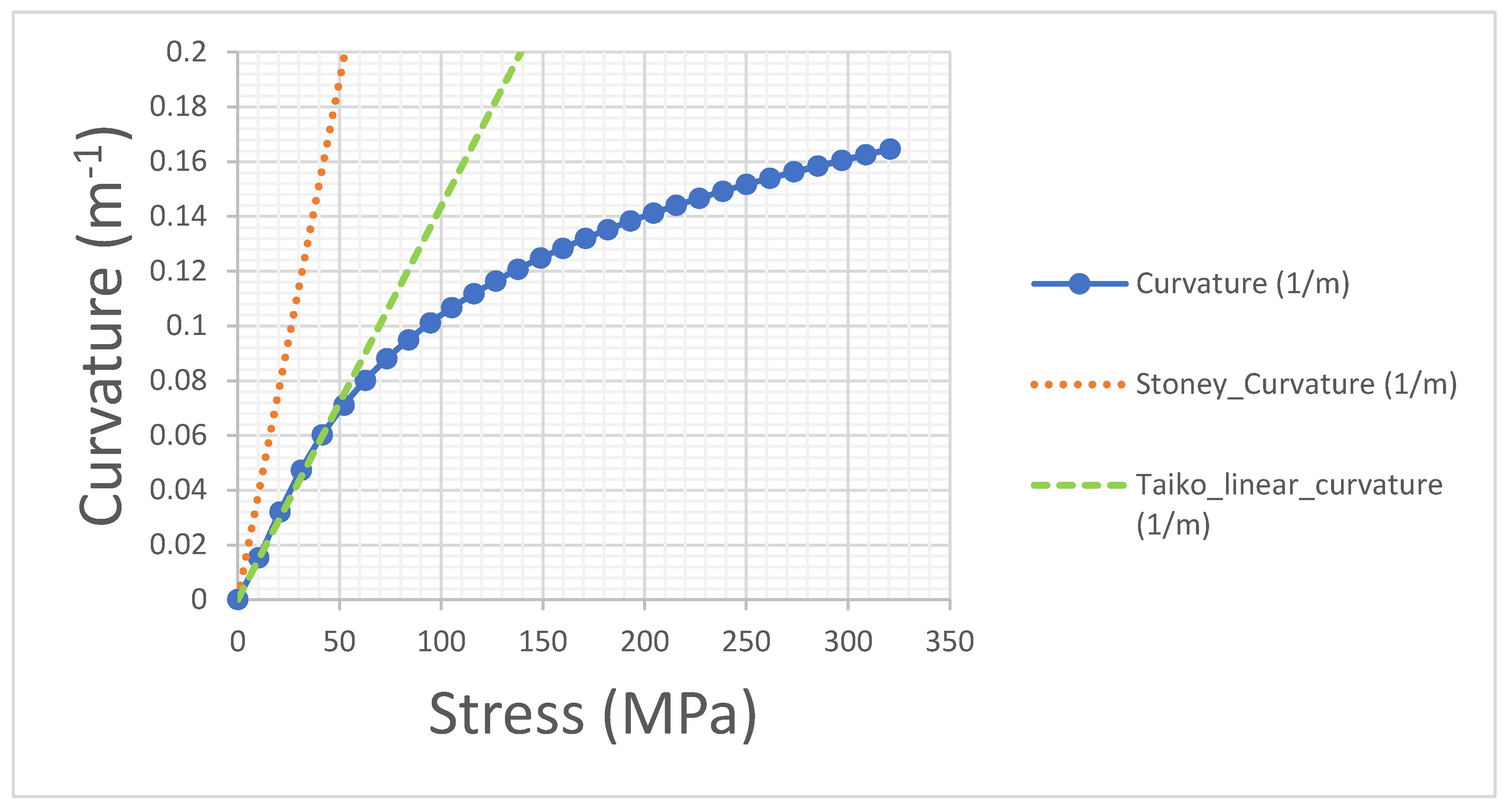
Figure 7.
Curvature as a function of the stress for a taiko wafer with hs ranging in the interval 100 - 400 µm and the other quantities fixed to the typical value reported in Table 1.
Figure 7.
Curvature as a function of the stress for a taiko wafer with hs ranging in the interval 100 - 400 µm and the other quantities fixed to the typical value reported in Table 1.
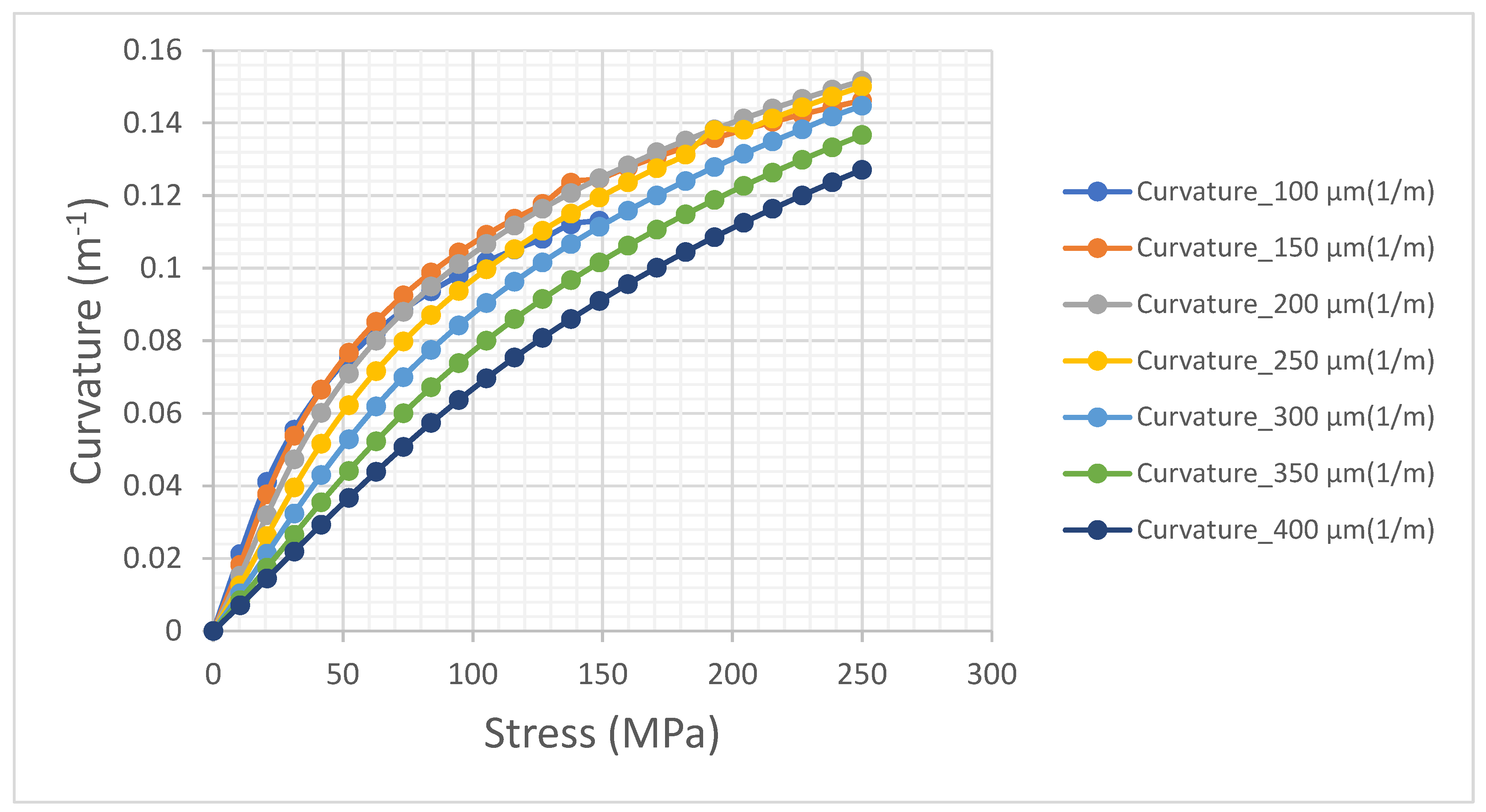
Figure 8.
Slope in the linear case for a taiko wafer reported as a function of the substrate thickness in µm and its comparison with the slope provided by the Stoney Equation.
Figure 8.
Slope in the linear case for a taiko wafer reported as a function of the substrate thickness in µm and its comparison with the slope provided by the Stoney Equation.
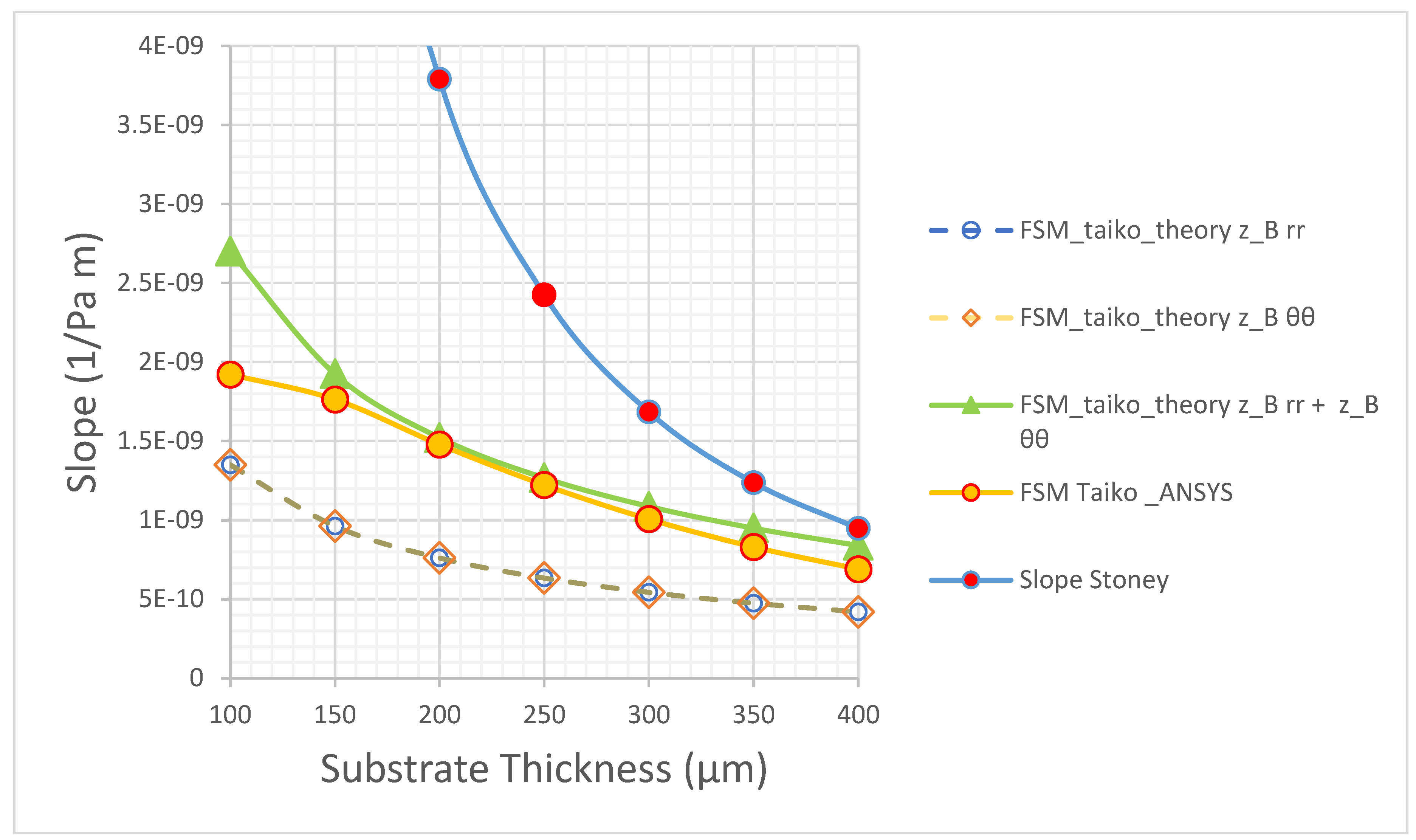
Figure 9.
Equivalent thickness of a FSM-taiko wafer as a function of the substrate thickness.
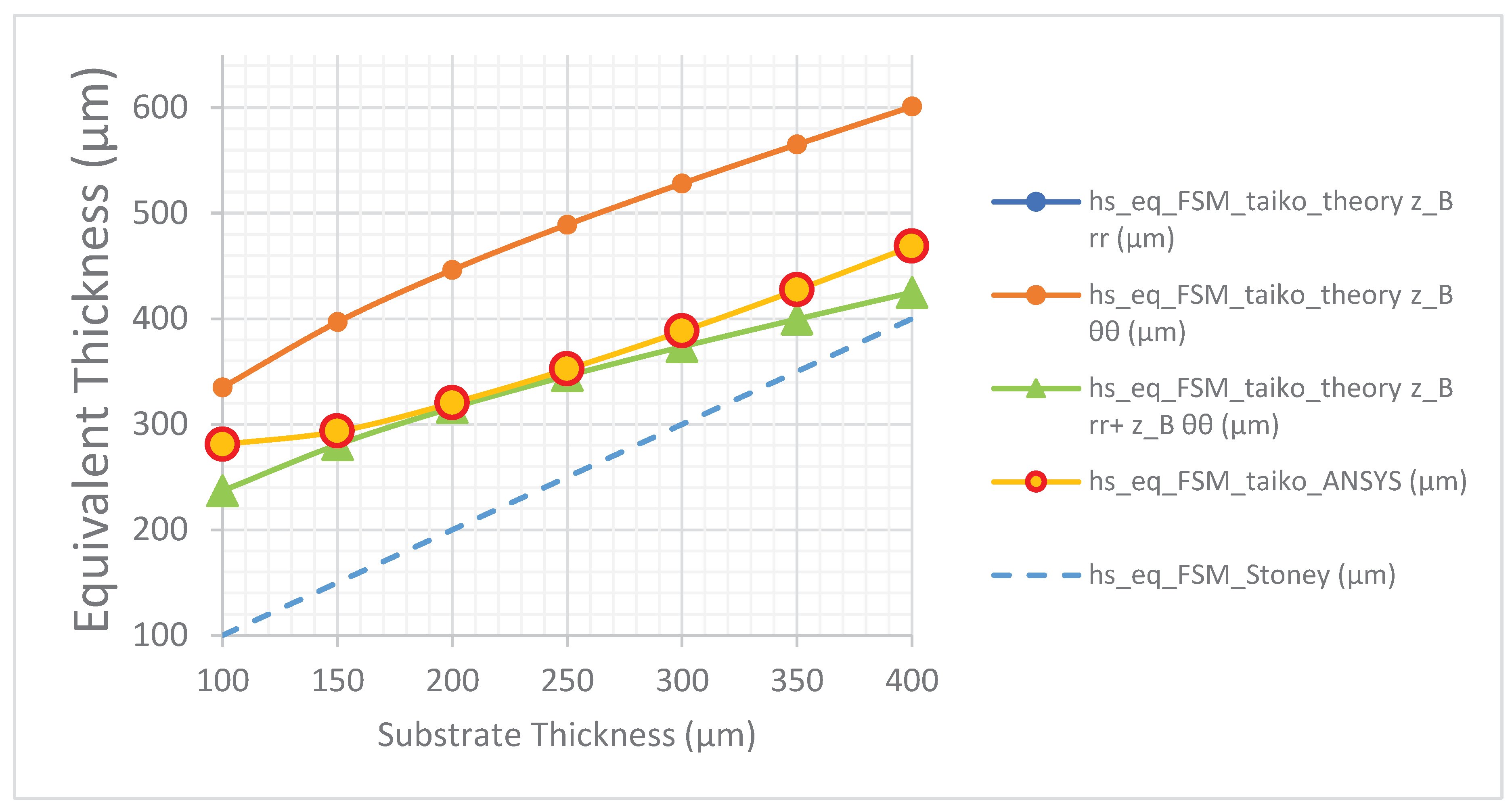
Table 1.
Look-up table reporting the typical value of the geometrical properties of the investigated FSM-taiko wafer.
Table 1.
Look-up table reporting the typical value of the geometrical properties of the investigated FSM-taiko wafer.
| Symbol | Quantity | Typical Value |
|---|---|---|
| hs | Substrate Thickness (µm) | 100 |
| H-hs | Step height (µm) | 450 |
| hf | Front Side Metal thickness (µm) | 4.5 |
| Rext-Rint | Ring width (mm) | 3.7 |
Disclaimer/Publisher’s Note: The statements, opinions and data contained in all publications are solely those of the individual author(s) and contributor(s) and not of MDPI and/or the editor(s). MDPI and/or the editor(s) disclaim responsibility for any injury to people or property resulting from any ideas, methods, instructions or products referred to in the content. |
© 2023 by the authors. Licensee MDPI, Basel, Switzerland. This article is an open access article distributed under the terms and conditions of the Creative Commons Attribution (CC BY) license (http://creativecommons.org/licenses/by/4.0/).
Copyright: This open access article is published under a Creative Commons CC BY 4.0 license, which permit the free download, distribution, and reuse, provided that the author and preprint are cited in any reuse.


