Submitted:
01 June 2018
Posted:
04 June 2018
You are already at the latest version
Abstract
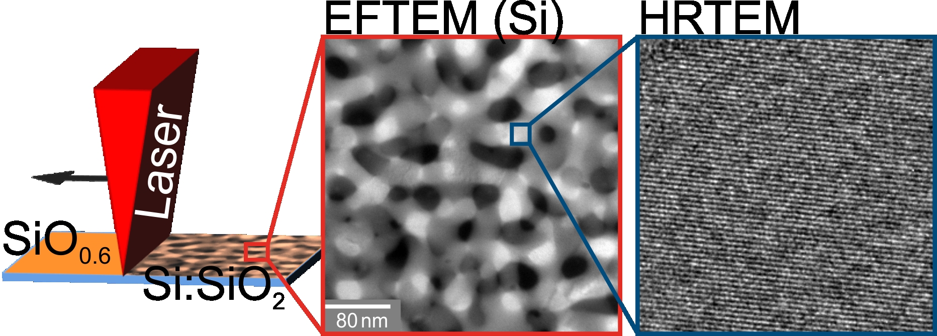
Three-dimensional nanocomposite networks consisting of percolated Si nanowires in a SiO2 matrix, Si:SiO2, were studied. The structures were obtained by reactive ion beam sputter deposition of SiOx (x ≈ 0.6) thin films at 450 °C and subsequent crystallization using conventional oven as well as millisecond line focus laser annealing. Rutherford backscattering spectrometry, Raman spectroscopy, X-ray diffraction, cross-sectional and energy-filtered transmission electron microscopy were applied for sample characterization. While oven annealing resulted in a mean Si wire diameter of 10 nm and a crystallinity of 72 % within the Si volume, almost single-domain Si structures with 30 nm in diameter and almost free of amorphous Si were obtained by millisecond laser application. The structural differences are attributed to the different crystallization processes: Conventional oven tempering proceeds via solid state, millisecond laser application via liquid phase crystallization of Si. The 5 orders of magnitude larger diffusion constant in the liquid phase is responsible for the three times larger Si nanostructure diameter. In conclusion, laser annealing offers not only significantly shorter process times but moreover a superior structural order of nano-Si compared to conventional heating.
Keywords:
silicon
; nanostructures
; percolated networks
; nanocomposites
; thin films
; laser processing
; phase separation
; liquid phase crystallization
Copyright: This open access article is published under a Creative Commons CC BY 4.0 license, which permit the free download, distribution, and reuse, provided that the author and preprint are cited in any reuse.


