

Submitted:
23 October 2026
Posted:
26 October 2026
You are already at the latest version
Abstract
Flexible short-wave infrared (SWIR) photodetectors are critical for versatile emerging applications, including wearable health monitors, artificial vision, and curved-surface imaging systems. Nevertheless, conventional SWIR photodetectors struggle to achieve mechanical flexibility due to their intrinsic rigidity and high-temperature processing requirements. Herein, we report flexible, self-powered SWIR image sensors based on Te0.62Se0.38/MoS2 heterojunctions. Their staggered type-II band alignments facilitate efficient photocarrier separation, demonstrating a broadband photoresponse extending to a cut-off wavelength of 1700 nm, a linear dynamic range of over 80 dB, an exceptional photo-to-dark current ratio exceeding 105, and a room-temperature specific detectivity of 1.8×10⁹ Jones for 1550 nm illumination. Benefiting from these superior optoelectronic properties, self-powered SWIR single-pixel imaging and optical communication applications were realized. Furthermore, taking advantage of the unique one-dimensional helical chain structure of the Te-Se alloy and the ultrathin nature of MoS2, heterojunction devices fabricated on flexible polyimide substrates exhibit outstanding mechanical endurance, retaining their initial response even at a bending radius of 4 mm. These findings highlight the considerable potential of Te-Se/MoS2 heterojunctions as a versatile material platform for flexible SWIR optoelectronics and provide a promising avenue toward next-generation wearable and intelligent sensing systems.
Keywords:
self-powered photodetector
; SWIR imaging
; flexible optoelectronics
; Te-Se alloy
1. Introduction
Flexible photodetectors have emerged as a pivotal paradigm in modern optoelectronics, offering transformative potential across multiple next-generation frontiers, including wearable bioelectronics, soft robotics, bio-inspired neuromorphic vision systems, and flexible optical communication networks [1]. Despite substantial progress, the majority of flexible photodetectors remain constrained to the visible and near-infrared regions. Short-wave infrared (SWIR) imaging captures significantly richer information than visible light and maintains robust performance in adverse weather conditions (e.g., fog, haze, and smoke), unlocking a wide range of new advanced capabilities [2,3,4]. Nevertheless, realizing flexible SWIR photodetectors presents more critical material and processing challenges. Conventional SWIR detectors, typically based on InGaAs, HgCdTe, InAs/GaSb, and Ge, rely heavily on high-temperature epitaxy on lattice-matched rigid substrates [5]. This inherent mechanical brittleness, coupled with demanding thermal budgets, significantly hinders their integration into flexible platforms. Furthermore, in contrast to the vast library of visible light-sensitive semiconductors, the number of novel narrow-bandgap materials capable of SWIR absorption and low-temperature synthesis is very limited.
The recent emergence of tellurium-selenium (Te-Se) alloys with great potential in high-performance optoelectronics has attracted increasing attention as a promising material platform [6,7,8,9,10]. Broadly, Te-Se alloys offer unique advantages that make them highly promising for flexible SWIR photodetectors for the following reasons. First, both Te and Se share the same trigonal crystal structure featuring parallel spiral chains of atoms packed together in a hexagonal array [11,12]. These helix-structured Te-Se chains confer a low elastic modulus and exceptional strain tolerance along the chain axis (c-axis) [5,13,14]. Second, Te-Se alloys across their entire compositional range can be readily synthesized without phase separation, allowing their optical bandgaps to be continuously tuned from ~0.35 eV to 1.8 eV through precise stoichiometric control [15,16]. This broad spectral coverage spans the entire SWIR region. Furthermore, the stoichiometry-modulated band structure of these p-type Te-Se alloys provides versatile options for constructing photovoltaic SWIR photodetectors when paired with suitable complementary n-type semiconductors. Compared to their photoconductive counterparts, self-powered (photovoltaic) devices can effectively suppress dark current density, thereby significantly enhancing the signal-to-noise ratio [17,18,19]. Importantly, Te-Se alloys possess low melting points and facilitate wafer-scale synthesis on the conventional flexible polymer substrates via thermal evaporation and magnetron sputtering method [20,21]. Furthermore, Te-Se alloys demonstrate superior ambient stability compared to other SWIR-sensitive semiconductors, such as lead sulfide quantum dots and black phosphorus [22]. Our ongoing research indicates that unencapsulated Te-Se alloy-based transistors retain their electrical performance even after six months of ambient storage.
To date, most reported Te-Se alloy-based photovoltaic detectors rely on heterojunctions formed on rigid substrates, such as Te-Se/ZnO [22], Te-Se/SnO2 [23], Te-Se/Si [24], and Te-Se/GaAs [20,25]. The demonstration of flexible self-powered SWIR photodetectors remains scarce [5]. Moreover, despite considerable research efforts, Te-Se alloy-based photodetectors still face critical challenges such as high dark current and limited photo-to-dark current ratios. In particular, previously reported detectors generally exhibit very low open-circuit voltages under SWIR illumination. Two-dimensional transition metal dichalcogenides (TMDCs) with atomic-scale thickness and exceptional mechanical flexibility have been considered prime candidates for next-generation electronics and optoelectronics [26,27]. However, flexible self-powered SWIR photodetectors formed by integrating Te-Se alloys with TMDCs have not yet been reported.
In this study, we demonstrate a flexible, self-powered SWIR photodetector based on a Te0.62Se0.38/MoS2 heterojunction platform. By leveraging the interfacial type-II band alignment, the fabricated heterostructure photodiode delivers high-performance photovoltaic SWIR detection, featuring an extended cut-off wavelength of 1700 nm, an 80 dB linear dynamic range, an ultrahigh photo-to-dark current ratio exceeding 105, and a peak room-temperature specific detectivity of 1.8×10⁹ Jones under 1550 nm excitation. The self-powered operation enables practical applications in single-pixel SWIR imaging and wireless optical communication. Furthermore, exploiting the intrinsic one-dimensional helical atomic chain structure of the Te-Se alloy alongside the atomically thin MoS2 layer, the heterojunction devices integrated on flexible polyimide substrates exhibit exceptional mechanical robustness, maintaining their initial response down to a bending radius of 4 mm. This work underscores the compelling potential of Te-Se/TMDCs heterostructures for next-generation flexible SWIR optoelectronics and conformable intelligent sensing systems.
2. Materials and Methods
2.1. Material Synthesis and Characterizations
Monolayer n-type MoS2 was synthesized via atmospheric pressure chemical vapor deposition using a liquid molybdenum precursor [28]. Prior to synthesis, the c-plane sapphire substrate (1 cm× 1 cm) was pretreated with O2 plasma (120 W, 60 s). An aqueous precursor solution was prepared by dissolving 40 mg of Na2MoO3 in 10 mL of deionized water and subsequently spin-coated onto the pretreated substrate at 4000 rpm for 60 s. After being dried on a hot plate at 150 ℃ for 10 s, the substrate was transferred to a quartz boat located at the center of a three-zone tube furnace. Sulfur powder (300 mg) was positioned ~30 cm upstream of the substrate. The chamber was first evacuated and purged three times with 300 sccm of Ar gas. The temperatures of the sulfur and substrate zones were then ramped to 250 ℃ and 800 ℃, respectively, over 30 min and held for 10 min to grow MoS2. An Ar flow of 110 sccm was maintained throughout the growth process.
Te0.62Se0.38 thin films were deposited via thermal evaporation according to our previously established protocol [20]. Briefly, bulk Te0.62Se0.38 source material was first synthesized by alloying 15 g of Te and 5 g of Se powders (99.99% purity, Zhongnuo Advanced Material Technology Co., Ltd.) in a vacuum-sealed quartz tube at 560 ℃ for 24 h. During thermal evaporation, the deposition rate was controlled within 2-10 Å/s to achieve a nominal film thickness of ~80 nm. Subsequently, the as-deposited films were vacuum-annealed in a rapid thermal annealing furnace at 130 ℃ for 10 min to enhance their crystallinity.
The structural properties of the Te0.62Se0.38 film were characterized by X-ray diffraction (XRD, Rigaku SmartLab). The actual Te: Se atomic ratios were determined by energy-dispersive X-ray spectroscopy (EDX) coupled with scanning electron microscopy (SEM). Micro-Raman spectroscopy and photoluminescence measurements were conducted using a 532 nm excitation laser (Zolix RTS2).
2.2. Heterojunction Device Fabrication
Polyimide (PI) was employed as the flexible substrate for fabricating the Te0.62Se0.38/MoS2 heterojunction devices. The liquid PI precursor was spin-coated onto a SiO2/Si carrier substrate at 3000 rpm for 60 s and followed by a sequential thermal curing process at 100 °C for 30 min, 150 °C for 30 min, and 280 °C for 40 min. The MoS2 film was transferred onto the PI substrate using a poly(methyl methacrylate)-assisted wet transfer method [29]. Maskless ultraviolet photolithography (TTT-07-UV Litho-ACA) was then performed to define the active windows for Te0.62Se0.38 deposition, forming the Te0.62Se0.38/MoS2 heterojunctions. Ohmic electrodes of Au (50 nm) and Ti/Au (15 nm/40 nm) were deposited onto the Te0.62Se0.38 and MoS2 contact regions, respectively. Finally, the flexible PI substrate bearing the devices was delaminated from the underlying SiO2/Si carrier substrate. The fabrication of Te0.62Se0.38/MoS2 heterojunction on SiO2/p++-Si substrate follows a similar procedure.
2.3. Optoelectronic Performance Measurements
Optoelectronic performance of the device was evaluated at room temperature under ambient conditions using a semiconductor parameter analyzer (Keithley 4200-SCS) integrated with a probe station. Monochromatic laser illumination at 1342 nm, 1550 nm, and 1700 nm was focused onto the device via a 40× objective lens, producing a spot diameter of ~140 μm with tunable power density. Spatial photocurrent mapping was executed using a micro-nano spectral response system (Zolix DSR300). Single-pixel imaging was performed on a custom-built setup featuring two stepper motor actuators (Thorlabs DRV250) for precise X-Y stage positioning.
3. Results and Discussion
3.1. Optoelectronic Performance of Te0.62Se0.38/MoS2 Heterojunctions on SiO2/Si
Based on our previous study [20], Te-Se alloy film with a Te:Se atomic ratio of 0.62:0.38 was selected for device fabrication to optimize SWIR absorption while maintaining favorable energy band alignment with monolayer MoS2. While the precursor mass ratio of 15 g:5 g yields a nominal Te:Se atomic ratio of 0.65:0.35, the higher Se composition in the resulting film is attributed to the distinct vapor pressures of Te and Se (Figure S1) [6,30]. Prior to demonstrating flexible photodetectors, we first fabricated Te0.62Se0.38/MoS2 heterojunctions on rigid SiO2/p++-Si substrates and systematically evaluated their SWIR optoelectronic characteristics.
Schematic illustration of the Te0.62Se0.38/MoS2 heterojunction and a representative optical microscopy image of fabricated device are presented in Figure 1a and Figure 1b, respectively. The layer number and structural quality of the synthesized MoS2 were evaluated by Raman spectroscopy (Figure 1c, top) and photoluminescence spectroscopy (Figure S2). The Raman spectrum of MoS2 exhibits two dominant active modes: the in-plane mode at ~385.3 cm-1 and the out-of-plane A1g mode at ~403.5 cm-1. Their frequency difference is ~18.2 cm-1, which falls strictly within the benchmark range for monolayer MoS2 [31]. Together with a strong photoluminescence emission centered at the direct bandgap (~688 nm), these features unambiguously confirm the monolayer nature and high crystallinity of the MoS2 flakes [29]. Furthermore, the Raman spectrum of Te0.62Se0.38 displays characteristic peaks at 149.2 cm-1 and 175.3 cm-1 (Figure 1c, bottom), in excellent agreement with previous reports [30]. The n-type and p-type transport behavior of MoS2 and Te0.62Se0.38 were verified via the transfer characteristics of their respective field-effect transistors (Figure S3). Under strong 1342 nm illumination, the transfer curves of MoS2 remain virtually unchanged. Conversely, the Te0.62Se0.38 transistor exhibits a distinct current increase, demonstrating that Te0.62Se0.38 acts as the sole SWIR absorption layer in this device architecture.
Figure 1d presents the current-voltage (I-V) characteristics of the heterojunction in the dark and under 1342 nm, 1550 nm, and 1700 nm illumination. The device exhibits pronounced photovoltaic behavior, demonstrating its strong capability as a self-powered SWIR photodetector. Spatial photocurrent mapping at zero bias under 1313 nm laser illumination confirms that photocarrier generation and separation are primarily localized within the Te0.62Se0.38/MoS2 overlapping heterojunction area (Figure 1e and Figure S4). This self-powered photoresponse could be explained from the energy band alignment at the Te0.62Se0.38/MoS2 heterojunction interface (Figure 1f). Based on reported literature values, the conduction band and valence band edges are positioned at approximately -4.1 eV and -4.8 eV for Te0.62Se0.38, and -4.2 eV and -6.0 eV for monolayer MoS2, respectively [3,20,32,33]. This band configuration forms a staggered type-II heterojunction, establishing an interfacial built-in electric field directed from n-MoS2 to p-Te0.62Se0.38. Under SWIR excitation, photogenerated electron-hole pairs in Te0.62Se0.38 are rapidly dissociated by this built-in electric field. The electrons and holes subsequently drift to MoS2 and Te0.62Se0.38 layer, respectively, enabling efficient self-powered photodetection at zero bias.
Figure 2a and Figure 2b illustrate the I-V characteristics of the heterojunction photodetector under varying excitation power densities at 1313 nm and 1550 nm, both demonstrating pronounced photovoltaic behavior. Benefiting from the high crystalline quality of the monolayer MoS2 and Te0.62Se0.38 alloy film, the device exhibits an ultra-low dark current density of 1.4×10⁻⁸ A cm-2 at zero bias. Consequently, remarkable photo-to-dark current ratios of 4.3×10⁵ and 1.9×10⁵ are achieved at 1313 nm and 1550 nm (Figure 2c and Figure 2d), respectively, outperforming most previously reported Te-Se alloy-based photodetectors [3,10,20,22,23,34,35,36]. In addition, maximum open-circuit voltages (Voc) of 0.31 V (1313 nm) and 0.24 V (1550 nm) are obtained, which are among the highest values reported for photodiodes under SWIR illumination. Figure 2e plots the zero-bias photocurrent (Iph, top panel) and Voc (bottom panel) as a function of optical power density under 1550 nm illumination. The Iph scales monotonically with incident optical power following a power-law relationship Iph=α•Pθ, yielding an exponent of approximately 0.83 across the measured range, which corresponds to a broad linear dynamic range of over 80 dB. Moreover, the Voc exhibits a logarithmic growth with excitation power prior to saturating at higher intensities. This behavior agrees well with ideal p-n junction photovoltaic theory [20], confirming that the photoresponse originates predominantly from the photovoltaic effect rather than photothermal mechanisms. Figure 2f shows the optical power-dependent responsivity (R, bottom panel) and shot noise-limited specific detectivity (D*, top panel) at 0 V bias. The device exhibits a peak R of 65.9 mA W-1 under a low illumination power of 3.2 μW cm-2 (1550 nm), corresponding to an external quantum efficiency (EQE) of 5.2%. Accordingly, a maximum D* of 1.8×10⁹ Jones is obtained. Figure 2g illustrates the dynamic photoswitching behavior of the photodiode for ~360 continuous on/off cycles within 30 min. Both the photocurrent and dark current are well-maintained with negligible fluctuation, demonstrating favorable operational reliability.
3.2. Flexible Te0.62Se0.38/MoS2 SWIR Photodetector on PI Substrate
With a peak thermal budget of less than 150 ℃, the overall heterojunction device fabrication process meets low-temperature manufacturing requirements, ensuring excellent compatibility with flexible, thermally sensitive polymer substrates. Figure 3a schematically illustrates the fabrication process for flexible Te0.62Se0.38/MoS2 SWIR photodetectors on a polyimide (PI) substrate. Here, PI was selected as the substrate owing to its superior thermal stability, mechanical flexibility, and chemical resistance [37,38]. Figure 3b presents optical photographs of the as-fabricated heterojunction photodetectors after they were peeled from the SiO2/Si carrier substrate, revealing their flexible and rollable characteristics in the free-standing state. Notably, SWIR photoresponse characterizations confirm that the flexible photodetectors retain robust photovoltaic behavior under both 1342 nm and 1550 nm excitation (Figure S5).
Figure 3c and Figure 3d display the I-V characteristics of the flexible device in the dark and under 1342 nm illumination, evaluated in both its flat state and a bent state with a 4 mm radius of curvature (RoC). This controlled bending state was achieved by conformally wrapping the flexible PI substrate around an acrylic cylinder of the corresponding radius (Figure 3d, inset). Figure 3e shows the statistical distributions of dark current and photocurrent in the flat and bent states. Despite a slight increase in dark current, the photocurrent of the photodetector in the bent state remains comparable to that in the flat state, validating the promise of Te0.62Se0.38/MoS2 heterojunctions for flexible SWIR optoelectronic applications. This favorable mechanical stability can be attributed to several key structural factors. First, X-ray diffraction analysis (Figure S6) reveals that the helical Te-Se atomic chains (c-axis) of Te0.62Se0.38, which possess a low elastic modulus and a high fracture strain, lie parallel to the PI substrate. Second, the atomically thin monolayer MoS2 exhibits exceptional mechanical flexibility, capable of withstanding elastic strains of 6%-11% prior to fracture [39]. Crucially, our evaluations on Te-Se alloy-based thin-film transistors reveal that the peak strain induced within the Te0.62Se0.38 film is less than 1% at a bending RoC of 4 mm, well below the failure threshold of either material.
3.3. Single-Pixel Imaging and Optical Communication Application
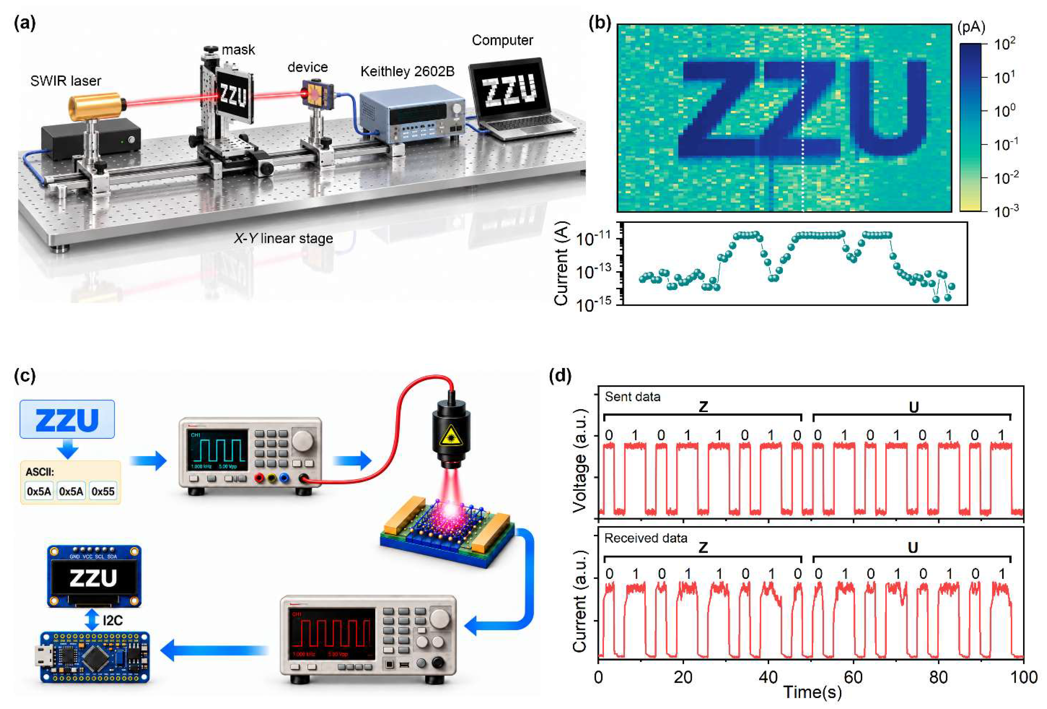
To further demonstrate the applicability of the Te0.62Se0.38/MoS2 heterojunction photodetector in SWIR imaging, a scanning-based single-pixel imaging system was constructed, as illustrated in Figure 4a. A shadow mask patterned with the letters “ZZU” was raster-scanned across a 1342 nm laser beam using a two-dimensional translation stage, while the corresponding photocurrent signals were simultaneously recorded. The spatial variation in optical transmittance between the transparent and opaque regions of the mask produced distinct photocurrent responses, enabling reconstruction of the target pattern by correlating the measured photocurrents with their spatial coordinates.[40] As shown in Figure 4b (top panel), the reconstructed photocurrent map clearly reproduces the “ZZU” pattern, with high- and low-photocurrent regions corresponding to the transparent and opaque areas, respectively. The photocurrent profile extracted along the white dotted line (Figure 4b, bottom panel) further reveals pronounced signal contrast between these regions, confirming the spatial discrimination capability of the imaging system. These results demonstrate the feasibility of the heterojunction photodetector for SWIR single-pixel imaging and spatial optical information acquisition.
Furthermore, the potential of the heterojunction photodetector for SWIR optical communication was evaluated using a proof-of-concept optical information transmission system, as illustrated in Figure 4c. The character string “ZU” was converted into the corresponding ASCII codes (0x5A and 0x55) and encoded into a 24-bit binary sequence (01011010 01010101). Pulse-width modulation (PWM) was employed to distinguish binary states “0” and “1” through different high-level durations, and the encoded electrical signals were used to modulate a 1342 nm laser, generating the optical pulse sequence shown in Figure 4d (top panel). At the receiving end, the flexible Te0.62Se0.38/MoS2 photodetector converted the modulated optical pulses into photocurrent signals under zero-bias conditions. The resulting signals were converted into voltage signals using a transimpedance amplifier (TIA) and recorded by an oscilloscope. As shown in Figure 4d (bottom panel), the recorded electrical response exhibits distinguishable pulses corresponding to the transmitted optical signals. Through signal filtering, threshold discrimination, and pulse-width-based decoding, the original 24-bit sequence and the message “ZU” were successfully recovered. For real-time information recognition, the decoding algorithm was further implemented on a microcontroller unit (MCU), which sampled the received signals through an analog-to-digital converter (ADC) at 1 kHz and displayed the decoded message on an OLED screen. These results highlight the potential of the flexible heterojunction photodetector for self-powered SWIR optical communication and real-time information processing.
4. Conclusions
In summary, we developed a flexible, self-powered SWIR photodetector platform by integrating a low-temperature-deposited Te0.62Se0.38 alloy film with monolayer MoS2. The engineered heterojunction diode facilitates efficient carrier separation, enabling robust photovoltaic detection up to 1700 nm with an ultralow dark current density of 1.4×10⁻⁸ A cm-2, a wide linear dynamic range of over 80 dB, a peak detectivity of 1.8×10⁹ Jones, and high photo-to-dark current ratios exceeding 105 for 1550 nm excitation. Moreover, by combining the low elastic modulus of helical Te-Se atomic chains with the mechanical compliance of 2D TMDCs, the device exhibits exceptional mechanical durability, retaining its photoresponse when bent to a radius of curvature as small as 4 mm. Its practical utility is further demonstrated through single-pixel SWIR optical imaging and wireless optical communication. This work establishes a scalable, low-temperature route to flexible SWIR optoelectronics and opens promising opportunities for conformable wearable electronics and intelligent vision systems.
Supplementary Materials
The following supporting information can be downloaded at the website of this paper posted on Preprints.org. Figure S1. SEM-EDX characterization results of Te0.62Se0.38 thin film. Figure S2. Photoluminescence spectrum of the monolayer MoS2. Figure S3. (a) Optical microscopy images of the individual MoS2 and Te0.62Se0.38 field-effect transistors (FETs). (b) Transfer characteristics (Ids-Vgs) of the MoS2 FET measured in the dark and under 1342 nm illumination. (c) Transfer characteristics of the Te0.62Se0.38 FET measured in the dark and under 1342 nm illumination. Figure S4. (a) Optical image of the Te0.62Se0.38/MoS2 heterojunction device utilized for spatial photocurrent mapping. (b) Photocurrent mapping at zero bias under 1313 nm illumination. Figure S5. I-V characteristics of the flexible Te0.62Se0.38/MoS2 heterojunction photodetector under 1342 nm and 1550 nm excitation. Figure S6. X-ray diffraction pattern of Te0.62Se0.38 thin film.
Author Contributions
P. L. conceived the idea, supervised the project, and wrote the original draft. C. J. K. performed material characterization, device fabrication, optoelectronic measurements, data collection and analysis. Y. B. H. assisted with the thermal evaporation of the Te-Se alloy film, photocurrent mapping, and single-pixel imaging measurements. Y. F. M. synthesized the monolayer MoS2. J. L. D. acquired funding and edited the manuscript. Z. J. X. provided research resources. All authors have read and agreed to the published version of the manuscript. C. J. K. and Y. B. H. contributed equally to this work.
Funding
This work is financially supported by the National Natural Science Foundation of China (52302162), Henan Provincial Key Science and Technology Research Projects (Grant No. 252102211102) and State Key Laboratory for Advanced Metals and Materials (Grant No. 2025-Z11).
Data Availability Statement
The original contributions presented in this study are included in the article/supplementary material. Further inquiries can be directed to the corresponding author(s).
Conflicts of Interest
The authors declare no conflicts of interest.
References
- Yang, G.; Li, J.; Wu, M.; Yu, X.; Yu, J. Recent advances in materials, structures, and applications of flexible photodetectors. Adv. Electron. Mater. 2023, 9, 2300340. [Google Scholar] [CrossRef]
- Gao, R.; Li, F.; Yang, H.; Yang, F.; Lin, L.; He, J.; Tang, Z.; Yang, X.; Dong, C.; Chen, C.; et al. Highly flexible TFT monolithic-integrated (Bi,Sb)2Se3 SWIR photodetector for wearable health monitoring and curved-surface imaging. iScience 2025, 28, 112008. [Google Scholar] [CrossRef]
- Wang, J.; Lin, P.; Wu, D.; Du, J.; Xie, Z.; Ke, C.; Wang, Y.; Hani, S. U.; Guo, Z.; Alam, T. I.; et al. Monolithic Te1-xSex-on-Si photodiodes for real-time short-wave infrared trajectory tracking. Adv. Funct. Mater. 2026, n/a, e78517. [Google Scholar] [CrossRef]
- Balendhran, S.; Mousavi Khaleghi, S. S.; Fan, D.; Crozier, K. B. Flexible infrared photodetectors: building blocks and prospects. npj Nanophotonics 2026, 3, 45. [Google Scholar] [CrossRef]
- He, Y.; Hu, Y.; Peng, M.; Fu, L.; Gao, E.; Liu, Z.; Dong, C.; Li, S.; Ge, C.; Yuan, C.; et al. One-dimensional crystal-structure Te-Se alloy for flexible shortwave infrared photodetector and imaging. Nano Lett. 2024, 24, 5774–5782. [Google Scholar] [CrossRef]
- Tan, C.; Amani, M.; Zhao, C.; Hettick, M.; Song, X.; Lien, D.-H.; Li, H.; Yeh, M.; Shrestha, V. R.; Crozier, K. B.; et al. Evaporated SexTe1-x thin films with tunable bandgaps for short-wave infrared photodetectors. Adv. Mater. 2020, 32, 2001329. [Google Scholar] [CrossRef]
- Liu, W.; Peng, M.; Chen, M.; Zhao, Y.; Yu, Y.; Jian, P.; Liu, Z.; Zeng, Y.; Luo, Y.; Tian, X.; et al. A Bias-tunable multispectral photodetector based on a GaN/TexSe1-x homo-type heterojunction with a unidirectional barrier. Adv. Sci. 2025, 12, 2417428. [Google Scholar] [CrossRef]
- Zha, J.; Tong, J.; Huang, H.; Xia, Y.; Dong, D.; Tan, C. A perspective on tellurium-based optoelectronics. Appl. Phys. Lett. 2024, 125, 070504. [Google Scholar] [CrossRef]
- Chen, Y.; Song, Z.; Liang, H.; Guan, X.; Ma, Y.; Zou, Y.; Huang, W.; Yang, M.; Zheng, Z.; Yao, J.; et al. Amorphous tellurium-selenium alloy: a promising candidate material toward broadband optoelectronics. Laser Photonics Rev. 2025, 19, e00586. [Google Scholar] [CrossRef]
- Li, R.; Yao, F.; Xu, Y.; Bai, S.; Jia, Z.; Lin, Q. Optimizing the charge carrier dynamics of thermal evaporated TexSe1-x films for high-performance short-wavelength infrared photodetection. Adv. Funct. Mater. 2024, 34, 2307005. [Google Scholar] [CrossRef]
- Yao, J.; Chen, F.; Li, J.; Du, J.; Wu, D.; Tian, Y.; Zhang, C.; Yang, J.; Li, X.; Lin, P. A high-performance short-wave infrared phototransistor based on a 2D tellurium/MoS2 van der Waals heterojunction. J. Mater. Chem. C 2021, 9, 13123–13131. [Google Scholar] [CrossRef]
- Geoffrion, L. D.; Guisbiers, G. Physico-chemical properties of selenium-tellurium alloys across the scales. Nanoscale Adv. 2021, 3, 4254–4270. [Google Scholar] [CrossRef]
- Ghosh, P.; Kahaly, M. U.; Waghmare, U. V. Atomic and electronic structures, elastic properties, and optical conductivity of bulk Te and Te nanowires: A first-principles study. Phys. Rev. B 2007, 75, 245437. [Google Scholar] [CrossRef]
- Dong, Y.; Zeng, B.; Zhang, X.; Li, D.; He, J.; Long, M. Study on the strain-induced mechanical property modulations in monolayer tellurene. J. Appl. Phys. 2019, 125, 064304. [Google Scholar] [CrossRef]
- Hadar, I.; Hu, X.; Luo, Z.-Z.; Dravid, V. P.; Kanatzidis, M. G. Nonlinear band gap tunability in selenium-tellurium alloys and its utilization in solar cells. ACS Energy Lett. 2019, 4, 2137–2143. [Google Scholar] [CrossRef]
- Zhang, Y.; Zhou, S.; Fan, H.; Wen, S.; Feng, Y.; Chen, H.; Zeng, H.; Wei, Y.; Lü, H.-F.; Yin, Y.; et al. Co-evaporated ratio-tunable TexSe1-x film for high-performance multiband photodetection toward subretinal color visual functions. Small 2026, 22, e74091. [Google Scholar] [CrossRef]
- Lin, P.; Yang, J. Tunable WSe2/WS2 van der Waals heterojunction for self-powered photodetector and photovoltaics. J. Alloys Compd. 2020, 842, 155890. [Google Scholar] [CrossRef]
- Yao, J.; Chen, F.; Li, J.; Du, J.; Wu, D.; Tian, Y.; Zhang, C.; Li, X.; Lin, P. Mixed-dimensional Te/CdS van der Waals heterojunction for self-powered broadband photodetector. Nanotechnology 2021, 32, 415201. [Google Scholar] [CrossRef]
- Du, J.; Liao, Q.; Liu, B.; Zhang, X.; Yu, H.; Ou, Y.; Xiao, J.; Kang, Z.; Si, H.; Zhang, Z.; et al. Gate-controlled polarity-reversible photodiodes with ambipolar 2D semiconductors. Adv. Funct. Mater. 2021, 31, 2007559. [Google Scholar] [CrossRef]
- Guo, Z.; Wang, J.; Du, J.; Wu, D.; Zeng, L.; Tsang, Y. H.; Wu, D.; Wang, Y.; Ding, Y.; Lin, P. Self-driven Te0.65Se0.35/GaAs SWIR photodiode with spectral response to 1.55 μm for broadband imaging and optical communication. Nano Energy 2025, 133, 110452. [Google Scholar] [CrossRef]
- Xu, M.; Lan, C.; Zeng, J.; Yin, Y.; Li, C. Research progress on TeSe-alloy-based heterojunction photodetectors. Photonics 2025, Vol. 12, 1190. [Google Scholar] [CrossRef]
- Fu, L.; He, Y.; Zheng, J.; Hu, Y.; Xue, J.; Li, S.; Ge, C.; Yang, X.; Peng, M.; Li, K.; et al. TexSe1-x photodiode shortwave infrared detection and imaging. Adv. Mater. 2023, 35, 2211522. [Google Scholar] [CrossRef]
- Hu, M.; Duan, Y.; Li, S.; Yang, L.; Dong, W.; Dang, W.; Zhang, Z.; Liu, J.; Li, Z. Molecular engineering of hole-selective layer of TexSe1-x for high-performance short-wave infrared photodetectors. ACS Photonics 2025, 12, 932–943. [Google Scholar] [CrossRef]
- Hu, M.; Liu, C.; Wang, J.; Zhang, S.; Tao, J.; Yang, L.; Guo, Y.; Li, Z.; Chu, J. Te0.75Se0.25/Si/AZO dual-heterostructure photodetector for spectral selective imaging and secure optical communication. Laser Photonics Rev. 2026, 20, e01126. [Google Scholar] [CrossRef]
- Yang, C.; Yu, H.; Lian, Y.; Liu, Y.; Wu, M.; Yang, X.; Han, J.; Dong, X.; Gou, J.; Zheng, X.; et al. High-speed short infrared detector based on vertical Gr/Se0.2Te0.8/GaAs heterojunction. Laser Photonics Rev. 2024, 18, 2400561. [Google Scholar] [CrossRef]
- Pan, H.; Liu, J.-Q.; Bi, J.; Xiao, W.; Xu, Z.; Gao, C.; Aierken, A.; Wang, G.; Liu, X.; Wu, Y.; et al. Transition metal dichalcogenides-based flexible transistors: from material and interface engineering to intelligent system integration. Mater. Des. 2026, 271, 117130. [Google Scholar] [CrossRef]
- Sumesh, C. K.; Patel, R.; Shah, P.; Pataniya, P. M. Flexible and wearable WSe₂ optoelectronics: current progress, technological challenges, and future directions. Nanoscale Adv. 2026. [Google Scholar] [CrossRef]
- Yu, L.; Tan, J.; Ma, H.; Liu, B.; Kang, F.; Lv, R. Large-area monolayer p-type semiconductor films toward high-performance electrical device arrays. Adv. Mater. 2025, 37, e00886. [Google Scholar] [CrossRef]
- Lin, P.; Zhu, L.; Li, D.; Xu, L.; Pan, C.; Wang, Z. Piezo-phototronic effect for enhanced flexible MoS2/WSe2 van der Waals photodiodes. Adv. Funct. Mater. 2018, 28, 1802849. [Google Scholar] [CrossRef]
- Huang, H.; Zha, J.; Xu, S.; Yang, P.; Xia, Y.; Wang, H.; Dong, D.; Zheng, L.; Yao, Y.; Zhang, Y.; et al. Precursor-confined chemical vapor deposition of 2D single-crystalline SexTe1-x nanosheets for p-type transistors and inverters. ACS Nano 2024, 18, 17293–17303. [Google Scholar] [CrossRef]
- Lee, C.; Yan, H.; Brus, L. E.; Heinz, T. F.; Hone, J.; Ryu, S. Anomalous lattice vibrations of single- and few-layer MoS2. ACS Nano 2010, 4, 2695–2700. [Google Scholar] [CrossRef]
- Kang, J.; Tongay, S.; Zhou, J.; Li, J.; Wu, J. Band offsets and heterostructures of two-dimensional semiconductors. Appl. Phys. Lett. 2013, 102, 012111. [Google Scholar] [CrossRef]
- Panasci, S. E.; Schilirò, E.; Greco, G.; Fiorenza, P.; Roccaforte, F.; Esposito, F.; Píš, I.; Bondino, F.; Madonia, A.; Cannas, M.; et al. Energy band alignment and electro-optical behavior of nearly unstrained monolayer MoS2 heterostructures with GaN. Adv. Mater. Interfaces 2026, 13, e00002. [Google Scholar] [CrossRef]
- Song, X.; Liu, J.; Wu, J.; Liu, S.; Wang, Y.; Fan, Y.; Zhou, Q. a.; Cheng, M.; Wang, F. A vacuum environment mediated annealing strategy for high-crystallized TexSe1-x films enabling efficient infrared photodetection. Mater. Sci. Semicond. Process. 2026, 214, 110875. [Google Scholar] [CrossRef]
- Li, R.; Bai, S.; Jia, Z.; Chen, X.; Liu, Y.; Lin, Q. Flexible broadband photodiodes based on amorphous Te0.4Se0.6 Thin Films. ACS Photonics 2024, 11, 2521–2527. [Google Scholar] [CrossRef]
- Lu, X.; Zhang, S.; Hao, S.; Zou, S.; Xu, H.; He, L.; Zhang, S.; Zhou, J.; Peng, A.; Liu, G.; et al. High-performance inverse opal SnO2/Te0.4Se0.6 photodetector for optical communication and health monitoring. Adv. Opt. Mater. 2025, 13, e01783. [Google Scholar] [CrossRef]
- Zhang, T.; Chai, Y.; Wang, S.; Yu, J.; Jiang, S.; Zhu, W.; Fang, Z.; Li, B. Recent study advances in flexible sensors based on polyimides. Sensors 2023, 23, 9743. [Google Scholar] [CrossRef]
- Lin, J.; Su, J.; Weng, M.; Xu, W.; Huang, J.; Fan, T.; Liu, Y.; Min, Y. Applications of flexible polyimide: barrier material, sensor material, and functional material. Soft Sci. 2023, 3, 2. [Google Scholar] [CrossRef]
- Bertolazzi, S.; Brivio, J.; Kis, A. Stretching and breaking of ultrathin MoS2. ACS Nano 2011, 5, 9703–9709. [Google Scholar] [CrossRef]
- Deng, W.; Zheng, Z.; Li, J.; Zhou, R.; Chen, X.; Zhang, D.; Lu, Y.; Wang, C.; You, C.; Li, S.; et al. Electrically tunable two-dimensional heterojunctions for miniaturized near-infrared spectrometers. Nat. Commun. 2022, 13, 4627. [Google Scholar] [CrossRef]
Figure 1.
(a) Schematic illustration of the Te0.62Se0.38/MoS2 heterojunction SWIR photodetector fabricated on a SiO2/p++-Si substrate. (b) Representative optical microscopy image of the fabricated device. (c) Raman spectra of monolayer MoS2 and the Te0.62Se0.38 thin film. (d) Current-voltage characteristics of the heterojunction device in the dark and under 1342 nm, 1550 nm, and 1700 nm illumination. (e) Spatial photocurrent mapping of the device under 1313 nm illumination at zero bias. The regions enclosed by red, white, blue, and purple dotted lines correspond to Te0.62Se0.38 film, monolayer MoS2, Au electrode, and Ti/Au contact electrode, respectively. (f) Schematic energy band diagram at the Te0.62Se0.38/MoS2 heterojunction interface.
Figure 1.
(a) Schematic illustration of the Te0.62Se0.38/MoS2 heterojunction SWIR photodetector fabricated on a SiO2/p++-Si substrate. (b) Representative optical microscopy image of the fabricated device. (c) Raman spectra of monolayer MoS2 and the Te0.62Se0.38 thin film. (d) Current-voltage characteristics of the heterojunction device in the dark and under 1342 nm, 1550 nm, and 1700 nm illumination. (e) Spatial photocurrent mapping of the device under 1313 nm illumination at zero bias. The regions enclosed by red, white, blue, and purple dotted lines correspond to Te0.62Se0.38 film, monolayer MoS2, Au electrode, and Ti/Au contact electrode, respectively. (f) Schematic energy band diagram at the Te0.62Se0.38/MoS2 heterojunction interface.
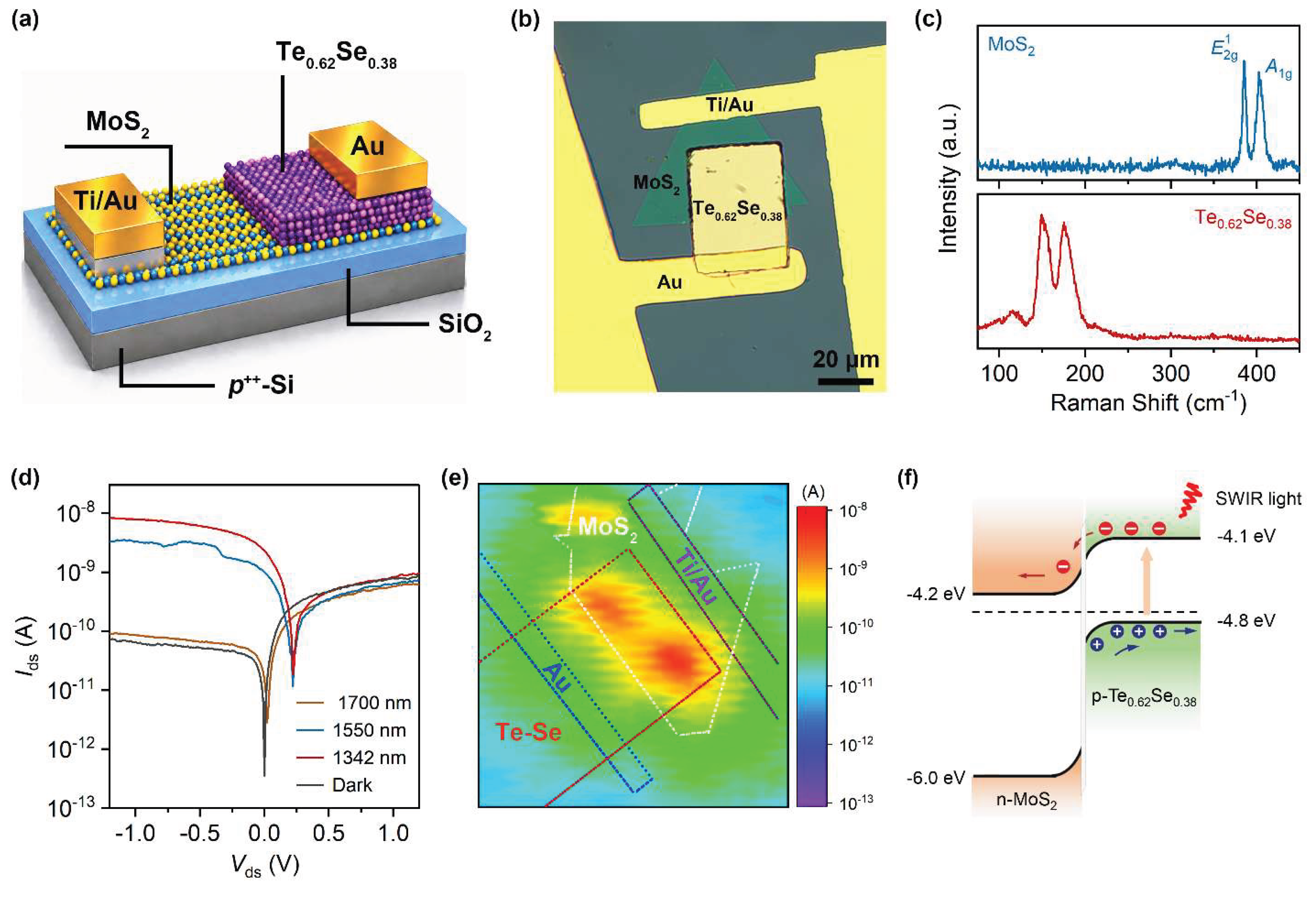
Figure 2.
I-V characteristics of the heterojunction device under varying illumination power densities at (a) 1313 nm and (b) 1550 nm excitation. Zero-bias temporal photoresponse under (c) 1313 nm and (d) 1550 nm laser excitation across different power densities. (e) Photocurrent (Iph) and Voc as a function of optical power density under 1550 nm illumination. (f) Incident power density-depednent R and D* under self-powered operation. (g) Dynamic photoswitching behavior of the device for ~360 continuous cycles within 30 min.
Figure 2.
I-V characteristics of the heterojunction device under varying illumination power densities at (a) 1313 nm and (b) 1550 nm excitation. Zero-bias temporal photoresponse under (c) 1313 nm and (d) 1550 nm laser excitation across different power densities. (e) Photocurrent (Iph) and Voc as a function of optical power density under 1550 nm illumination. (f) Incident power density-depednent R and D* under self-powered operation. (g) Dynamic photoswitching behavior of the device for ~360 continuous cycles within 30 min.
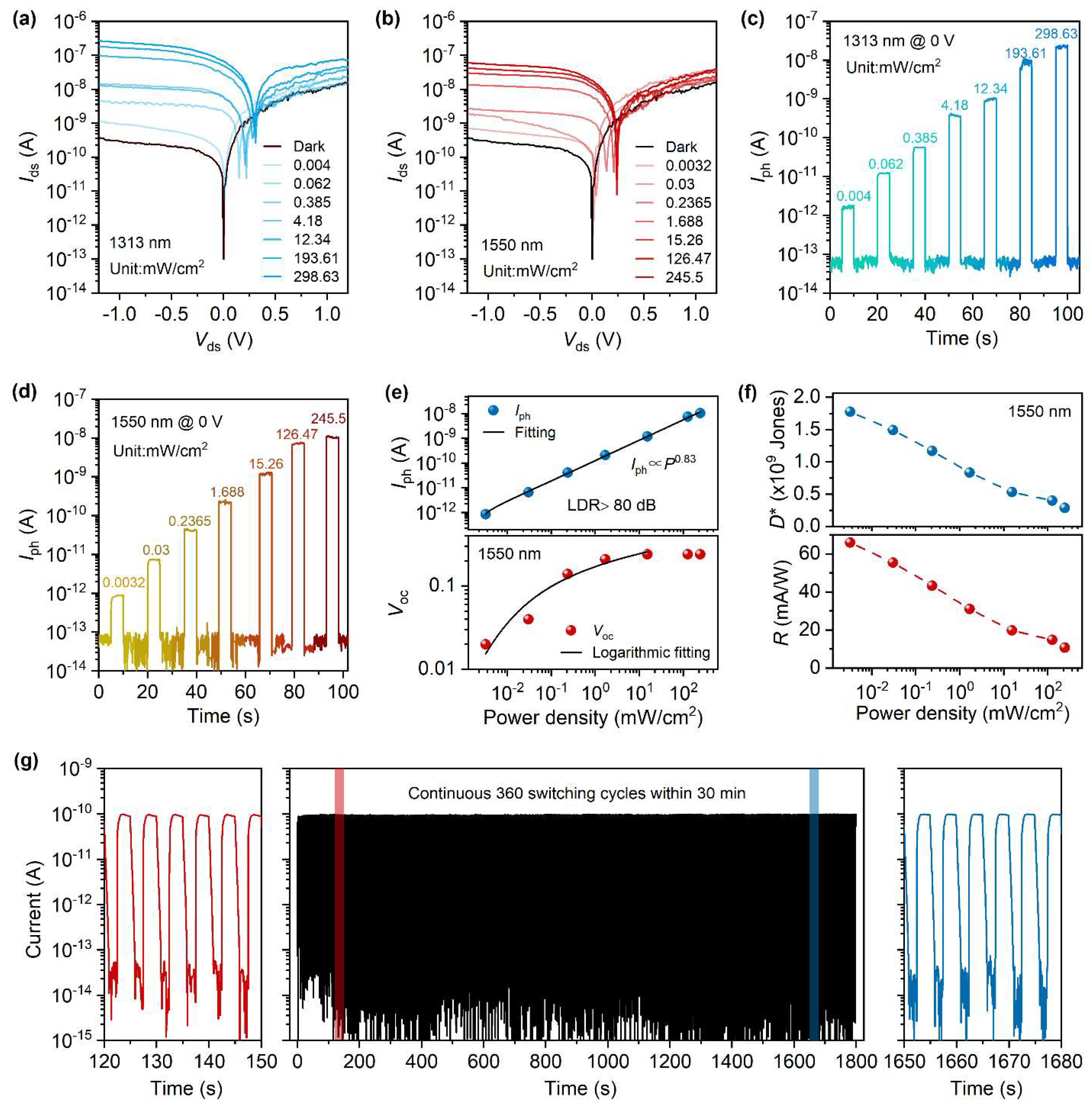
Figure 3.
(a) Schematic illustration of the fabrication process for flexible Te0.62Se0.38/MoS2 SWIR photodetectors. (b) Photographs of the as-fabricated photodetectors on a polyimide substrate. I-V characteristics of the flexible device in the dark and under 1342 nm illumination evaluated in (c) its flat state and (d) a bent state with a bending RoC of 4 mm. Insets show the corresponding photograph of the experimental setup. (e) Statistical distribution of dark current and photocurrent for the flexible photodetector in the flat and bent states.
Figure 3.
(a) Schematic illustration of the fabrication process for flexible Te0.62Se0.38/MoS2 SWIR photodetectors. (b) Photographs of the as-fabricated photodetectors on a polyimide substrate. I-V characteristics of the flexible device in the dark and under 1342 nm illumination evaluated in (c) its flat state and (d) a bent state with a bending RoC of 4 mm. Insets show the corresponding photograph of the experimental setup. (e) Statistical distribution of dark current and photocurrent for the flexible photodetector in the flat and bent states.
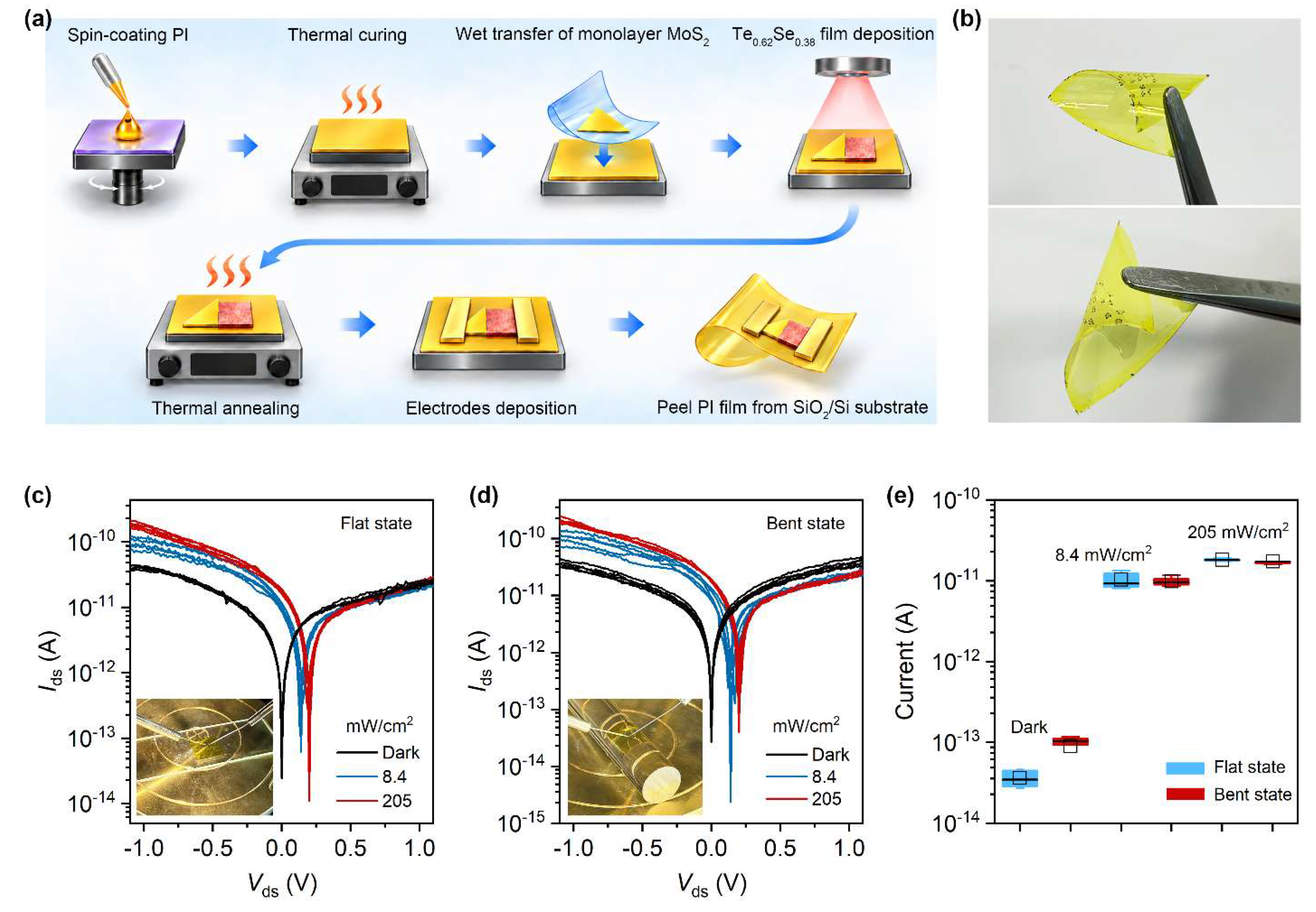
Figure 4.
(a) Schematic illustration of the experimental setup for single-pixel SWIR imaging. (b) Spatially resolved photocurrent map recorded under 1342 nm illumination using a shadow mask with a “ZZU” pattern (top panel) and the extracted photocurrent profile along the white dotted line (bottom panel). (c) Schematic diagram of the experimental configuration for self-powered SWIR optical communication. (d) Input 1342 nm optical signals programmed with the ASCII codes for the letters “ZU” (top panel) and the corresponding output photocurrent profile of the flexible Te0.62Se0.38/MoS2 heterojunction photodetector (bottom panel).
Figure 4.
(a) Schematic illustration of the experimental setup for single-pixel SWIR imaging. (b) Spatially resolved photocurrent map recorded under 1342 nm illumination using a shadow mask with a “ZZU” pattern (top panel) and the extracted photocurrent profile along the white dotted line (bottom panel). (c) Schematic diagram of the experimental configuration for self-powered SWIR optical communication. (d) Input 1342 nm optical signals programmed with the ASCII codes for the letters “ZU” (top panel) and the corresponding output photocurrent profile of the flexible Te0.62Se0.38/MoS2 heterojunction photodetector (bottom panel).
Disclaimer/Publisher’s Note: The statements, opinions and data contained in all publications are solely those of the individual author(s) and contributor(s) and not of MDPI and/or the editor(s). MDPI and/or the editor(s) disclaim responsibility for any injury to people or property resulting from any ideas, methods, instructions or products referred to in the content. |
© 2026 by the authors. Licensee MDPI, Basel, Switzerland. This article is an open access article distributed under the terms and conditions of the Creative Commons Attribution (CC BY) license (http://creativecommons.org/licenses/by/4.0/).
Copyright: This open access article is published under a Creative Commons CC BY 4.0 license, which permit the free download, distribution, and reuse, provided that the author and preprint are cited in any reuse.