

Submitted:
03 October 2026
Posted:
07 October 2026
You are already at the latest version
Abstract
Controlling heat flow in β-Ga₂O₃ thin films requires understanding both phonon transport within the semiconductor and heat transfer across metal/semiconductor interfaces. Here, we investigate these pathways in high-temperature RF magnetron-sputtered β-Ga₂O₃ films grown on c-plane sapphire with thicknesses from 0.42 to 2.1 μm. The thermal conductivity increases from 5.4–6.9 W m⁻¹ K⁻¹ in the 420 nm film to approximately 10–12 W m⁻¹ K⁻¹ in the thicker films. Structural characterization reveals thickness-dependent microstructural evolution, including grain coarsening and intergranular void-like defects. A semi-analytical Debye–Klemens model incorporating phonon scattering from film boundary and defects reproduces the overall thickness dependence. We further demonstrate that Ar plasma treatment provides an effective means of modifying interfacial heat transfer: the Al/β-Ga₂O₃ thermal boundary conductance increases from approximately 60 to 100 MW m⁻² K⁻¹, or by about 70%, while the thermal conductivity of the underlying β-Ga₂O₃ remains comparatively unchanged. Picosecond laser ultrasonic measurements and cross-sectional TEM reveal a corresponding modification of the interfacial acoustic response and formation of an ultrathin amorphous/disordered near-surface region. These results demonstrate that thermal transport in sputtered β-Ga₂O₃ can be independently tuned through film-thickness-dependent microstructure and near-surface interface modification, providing practical routes for thermal management in β-Ga₂O₃-based devices.
Keywords:
β-Ga₂O₃
; thermal conductivity
; thermal boundary conductance
; RF magnetron sputtering
; plasma treatment
; TDTR
; FDTR
1. Introduction
The development of high-power electronics has driven increasing interest in ultrawide-bandgap (UWBG) semiconductors capable of sustaining high electric fields and power densities. Among these materials, β-Ga₂O₃ has emerged as a promising candidate for next-generation power electronics owing to its ultrawide bandgap of approximately 4.8 eV, high critical electric field exceeding 8 MV/cm, and the availability of large-area single-crystal substrates produced by melt-growth techniques [1,2,3]. These characteristics make β-Ga₂O₃ attractive for high-voltage switches, power diodes, and other electronic devices operating under high electric-field and high-power-density conditions.
Despite these favorable electronic properties, thermal transport is a major limitation for β-Ga₂O₃-based electronics. The thermal conductivity of β-Ga₂O₃ is relatively low and strongly anisotropic, with reported values of approximately 10–30 W m⁻¹ K⁻¹ depending on crystallographic direction, substantially below those of established wide-bandgap semiconductors such as GaN and SiC [4,5,6]. The combination of high power density and low thermal conductivity can result in substantial self-heating near the active region, increasing device operating temperature and potentially degrading performance and reliability [7,8]. Consequently, understanding and controlling heat transport in β-Ga₂O₃ is essential for realizing the full potential of its electronic properties.
For thin films, however, the relevant thermal conductivity can differ substantially from the intrinsic bulk value. Previous studies have demonstrated pronounced thickness- and microstructure-dependent thermal transport in β-Ga₂O₃ films prepared by different growth and transfer approaches [9,10,11,12,13,14]. Finite film thickness limits the mean free path of heat-carrying phonons through boundary scattering, while grain boundaries, point defects, strain, implantation-induced damage and other structural imperfections can provide additional phonon scattering channels. Accordingly, mechanically exfoliated single-crystal films generally exhibit increasing thermal conductivity with increasing thickness, approaching the corresponding bulk value, whereas deposited or defect-rich films often exhibit substantially lower thermal conductivities [9,10,11,12,13,14]. Establishing the relationship between film thickness, microstructure, and thermal conductivity is therefore important for realistic thermal design of β-Ga₂O₃ thin-film devices.
Radio-frequency (RF) magnetron sputtering is an attractive approach for β-Ga₂O₃ thin-film growth because of its relative simplicity, scalability, thickness control, and compatibility with large-area substrates. Previous studies have shown that the crystalline quality, preferred orientation, surface morphology, stoichiometry, and optoelectronic properties of RF-sputtered Ga₂O₃ are strongly influenced by deposition parameters such as substrate temperature, sputtering pressure, RF power, and substrate orientation [15,16,17,18]. In particular, optimization of the sputtering pressure and gas composition can substantially modify film crystallinity and surface morphology, while high-temperature RF sputtering has recently enabled highly crystalline β-Ga₂O₃ growth on sapphire substrates [16,18]. Nevertheless, compared with the extensive structural, optical, and electrical characterization of RF-sputtered β-Ga₂O₃, its thermal transport properties and their relationship with thickness-dependent microstructural evolution remain largely unexplored.
Thermal management, however, extends beyond heat transport within the semiconductor itself. In practical transistors and power diodes, heat generated near the active region must be dissipated across multiple interfaces, including those between β-Ga₂O₃ and metal contacts or thermal-management layers. In particular, metal contacts positioned near high-temperature regions of a device can provide an additional heat-removal pathway when their thermal boundary conductance (TBC) is sufficiently high [7,19]. Previous studies have demonstrated that thermal transport across metal/β-Ga₂O₃ interfaces is highly sensitive to interfacial structure, bonding, and chemical composition [19,20]. More recently, it was demonstrated that surface pretreatment and deposition conditions can substantially modify thermal conductance across Al/nonmetal interfaces by altering interfacial bonding strength, while leaving the thermal conductivity of the underlying material largely unaffected [21]. These results suggest that near-surface and interface engineering may provide an effective route for controlling heat transfer across metal/semiconductor interfaces.
Here, we investigate the thermal transport properties of high-temperature RF magnetron-sputtered β-Ga₂O₃ thin films over a range of thicknesses and correlate the measured thermal transport with their structural and morphological characteristics. We further demonstrate that RF plasma treatment of the β-Ga₂O₃ surface provides an effective means of modifying the thermal boundary conductance of an Al/β-Ga₂O₃ interface. By combining thermal measurements with electron microscopy, surface morphology characterization, and picosecond acoustic measurements, we establish a relationship between plasma-induced surface/interface modification and thermal transport across the Al/β-Ga₂O₃ interface. These results highlight the importance of both film microstructure and near-surface interface engineering for controlling thermal transport in sputtered β-Ga₂O₃ thin films.
2. Materials and Methods
2.1. Sample preparation
β-Ga₂O₃ thin films were deposited on (0001)-oriented c-plane sapphire substrates by high-temperature radio-frequency magnetron sputtering and hereafter referred to as RF-sputtered films, following the deposition protocol developed in our previous work [18]. Only the key growth parameters relevant to the present study are summarized here. A ceramic Ga₂O₃ target fabricated from 99.999% pure starting material was sputtered at an RF frequency of 13.56 MHz in a reactive Ar/O₂ atmosphere with an Ar:O₂ ratio of 1:1. The total working pressure was 1.07 Pa, the applied RF power was 100 W, and the target-to-substrate distance was 5 cm.
To enable efficient high-temperature heating of the infrared-transparent sapphire substrates, an approximately 1 μm-thick Ta layer was deposited on the backside of each substrate prior to β-Ga₂O₃ growth. The Ta coating enhanced absorption of thermal radiation from the heater and enabled stable heating of the sapphire substrates at the temperatures required for high-temperature growth. The β-Ga₂O₃ films investigated in this study were deposited at a substrate temperature of 1200 °C without post-growth annealing and had thicknesses ranging from approximately 0.42 to 2.1 μm.
The reproducibility of the deposition procedure was established in our previous study through multiple independent growth runs performed under identical nominal conditions. These experiments demonstrated reproducible structural and morphological characteristics across the sample series, while the substrate temperature was maintained within ±5 °C during deposition [18].
To investigate the effect of plasma-induced surface modification on thermal transport, three β-Ga₂O₃ samples, denoted S1, S2, and S3, were prepared in separate deposition runs under the same nominal growth conditions. Thus, the samples represented independently grown specimens produced using the same reproducible deposition protocol. Sample S1 was retained as an untreated reference, whereas samples S2 and S3 were subjected to RF Ar-plasma sputter treatment in the same magnetron sputtering system.
For the plasma treatment, each sample was placed directly on the surface of the same Ga₂O₃ target used for film deposition, within the magnetron erosion-track region. The sample covered most of the erosion track along the radial direction, while the remaining uncovered portion of the target continued to be sputtered during RF excitation. In this configuration, the β-Ga₂O₃ film surface was directly exposed to the near-target RF Ar plasma and sputtering environment, resulting in plasma- and sputter-induced surface modification. The treatments were carried out at the same total pressure used for film growth (1.07 Pa), but in pure Ar without O₂ addition. Samples S2 and S3 were treated at RF powers of 50 W for 5 min and 100 W for 2 min, respectively.
2.2. Structural characterization and surface morphology
The structural properties of the β-Ga₂O₃ thin films were characterized using X-ray diffraction (XRD), Raman spectroscopy, atomic force microscopy (AFM), high-resolution transmission electron microscopy (HRTEM) and scanning electron microscopy (SEM). XRD measurements were performed in powder diffraction geometry using a Rigaku SmartLab diffractometer with Cu Kα radiation over a 2θ range of 20°– 80° to evaluate the crystalline structure and phase composition of the films. Raman spectroscopy was carried out using a Horiba LabRAM micro-Raman system with excitation provided by a 532 nm single-mode laser (Torus 532, Laser Quantum). The system was equipped with a 50× objective lens, resulting in a laser spot diameter of approximately 1 µm. The spectra were collected using an 1800 grooves/mm grating with an acquisition time of 120 s. Surface morphology and roughness were investigated by AFM using a SmartSPM 1000 scanning probe microscope. Plan-view TEM lamellae were produced by FIB lift-out using a Thermo FISHER Helios 650 dual beam. Imaging was done at 200 kV in a JEOL ARM 200F. The evolution of film morphology and grain structure was further analyzed by SEM using a Crossbeam 540 microscope (Carl Zeiss).
2.3. Thermal transport measurements
Thermal transport measurements were performed using a time-domain thermoreflectance (TDTR) and frequency-domain thermoreflectance (FDTR) methods. Both setups are described in detail elsewhere [22-25]. Prior to TDTR measurements, an Al transducer layer with a thickness of approximately 80–90 nm was deposited onto the β-Ga₂O₃ films by magnetron sputtering. The thickness of the Al layer was determined by picosecond acoustic measurements and further confirmed by profilometry.
The TDTR system employed a Ti:sapphire mode-locked femtosecond laser (Tsunami, Spectra-Physics) operating at a wavelength of 782 nm, with a repetition rate of 80 MHz and a pulse duration of approximately 80 fs. The pump beam was modulated at a fixed frequency of approximately 10 MHz to periodically heat the Al transducer, while the time-delayed probe beam monitored the resulting thermoreflectance response. Both beams were focused and spatially overlapped on the sample surface using a 10× objective lens. The resulting beam diameter was ~ 13 µm, which is substantially larger than the thermal penetration depth at 10 MHz modulation frequency, providing predominantly cross-plane sensitivity. The measured ratio of the in-phase and out-of-phase lock-in signals, -Vin/Vout, as a function of pump–probe delay time was fitted using a multilayer heat-diffusion model [26] to extract the thermal conductivity of the β-Ga₂O₃ layer and the TBC of the Al/β-Ga₂O₃ interface.
Complementary FDTR measurements were performed using continuous-wave pump and probe lasers. Following the configuration described in our previous work [24, 25], 660 nm and 785 nm lasers were used as the pump and probe beams, respectively. The pump beam was periodically modulated at the frequencies ranging over 100 kHz to 3 MHz, while the reflected probe signal was detected using a photodetector connected to a lock-in amplifier. In contrast to TDTR, where the pump–probe time delay is varied, FDTR measurements were performed by sweeping the pump modulation frequency and recording the corresponding phase lag of the thermoreflectance response. The pump and probe beams were spatially overlapped and focused onto the Al transducer using a 60× objective lens, resulting in an effective pump–probe spot size of approximately 2–3 μm, consistent with the configuration used in our previous FDTR measurements. The measured phase response as a function of modulation frequency was fitted using a multilayer heat-diffusion model to extract the effective thermal conductivity of the β-Ga₂O₃ films [27].
The reliability of the fitted thermal parameters was evaluated by calculating the sensitivities of the TDTR and FDTR signals to the relevant model parameters (see Fig. S1 and Fig. S2, Supplementary Materials). The corresponding sensitivity coefficients and uncertainty analyses for both techniques, including the contributions from uncertainties in the Al transducer thickness, laser spot size, film thickness, thermophysical properties, and interfacial thermal conductance, are provided in the Supplementary Materials.
2.4. Semi-analytical thermal conductivity model
To gain more physical insights of the thickness-dependent thermal conductivity of β-Ga₂O₃, the thermal conductivity was modeled by Debye approximation based a semi-analytical phonon scattering model [28]:
where θD,j is the Debye temperature, τ is the total phonon relaxation time, T is the temperature, v is the average phonon velocity (4423 m/s [4]), and C(x) is the lattice specific heat defined as:
where kB is Boltzmann’s constant and ℏ is reduced Planck’s constant, x = ℏω/kBT. The sum was taken over the three main phonon branches: one longitudinal acoustic (LA) and two transverse acoustics (TA). The total relaxation time, τ(x), is given by Matthiessen’s rule:
and are Umklaap phonon-phonon, boundary and point defect scattering rates, respectively, defined as:
where M = 6.2231 × 10⁻²⁶ kg/atom is average atomic mass, γi is Grüneisen parameter, d is the sample thickness, V0 is the volume per atom, and Γ is the phonon scattering cross section.
The Debye model has been widely used to describe phonon transport and size-dependent thermal conductivity in β-Ga₂O₃ [4,5,29]. The intrinsic anisotropy of β-Ga₂O₃ is accounted for by using direction-specific model parameters; in the present work, the parameters corresponding to the (-201) orientation were adopted [4,29] (see Table 1).
3. Results
3.1. Structural and morphological evolution of β-Ga₂O₃ films with thickness
Figure 1 summarizes the structural characteristics of the β-Ga₂O₃ films with different thicknesses. Cross-sectional bright-field transmission electron microscopy (BF-TEM) images in Figure 1(a–c) reveal continuous β-Ga₂O₃ layers with thicknesses of approximately 420, 1100, and 2100 nm, respectively. All films exhibit a pronounced granular/columnar microstructure, while the characteristic dimensions of the crystalline domains evolve significantly with increasing film thickness. The 420 nm film consists of comparatively fine domains, whereas substantially larger crystalline regions are observed in 1100 and 2100 nm-thick films. Such microstructural evolution is consistent with progressive grain growth and competitive growth of neighboring crystalline domains during continued film deposition. However, higher-magnification BF-TEM images of the thicker films reveal additional structural imperfections, such as bright cavity-like regions, voids and intergranular porosity (see Fig. S3, Supplementary Materials). Nevertheless, some of the more diffuse BF-TEM contrast may also be attributed to a localized strain.
The surface morphology observed by SEM further supports this thickness-dependent microstructural evolution (see Fig. S4, Supplementary Materials). The 420 nm film exhibits relatively fine surface features with characteristic lateral dimensions of approximately 100–200 nm. A pronounced coarsening is observed for the 1100 nm film, where elongated surface features extend from several hundred nanometers to approximately 1–2 μm. In contrast, the characteristic lateral dimensions of the 2100 nm film are somewhat smaller, typically on the order of several hundred nanometers. The evolution of the surface morphology is therefore non-monotonic, where substantial coarsening occurs between 420 and 1100 nm, followed by a moderate reduction in characteristic lateral feature size for the thickest film.
The corresponding XRD patterns are also presented in Figure 1(d). All three films exhibit pronounced reflections at approximately 2θ ≈ 19°, 38°, and 59°, which were assigned to the (−201), (−402), and (−603) crystal planes of monoclinic β-Ga₂O₃, respectively, which is in agreement with previous reports on highly oriented β-Ga₂O₃ thin films grown by high-temperature sputtering and related epitaxial techniques [18,30]. No additional peaks related to other Ga₂O₃ polymorphs or secondary crystalline phases were detected within the sensitivity of the measurements geometry.
Raman spectroscopy measurements further confirmed the formation of monoclinic β-Ga₂O₃ in all investigated films, as shown in Figure 1(e). The spectra of all three films exhibit the characteristic Ag and Bg modes of β-Ga₂O₃, which are in good agreement with the reported Raman response of monoclinic β-Ga₂O₃ [31]. The positions of the principal Raman bands remain essentially unchanged among the three films, indicating preservation of the β-phase over the investigated thickness range. In addition, the Raman peak intensity increases systematically with increasing film thickness due to the increased sampling volume, which is in agreement with the improved crystalline ordering and grain coarsening observed by electron microscopy and XRD analyses.
The surface morphology of the β-Ga₂O₃ films was further examined by AFM over a scan area of 10 × 10 μm², as shown in Figure 2. The 420 nm film exhibits a relatively fine and uniform surface morphology with a surface roughness of approximately 1–2 nm. In contrast, the thicker films show a pronounced increase in surface topography, with roughness values in the range of approximately 20–30 nm. The 1100 nm film exhibits substantial lateral coarsening together with the formation of strongly faceted and elongated surface features, whereas the 2100 nm film retains a pronounced faceted morphology with a denser distribution of surface features. The AFM observations are consistent with the SEM results (see Supplementary Materials) and demonstrate a substantial evolution from a comparatively smooth, fine-featured surface in the thinnest film to a considerably rougher and more strongly faceted morphology in the thicker films. Together with the SEM and TEM observations, the AFM results indicate that film thickening is accompanied by pronounced domain coarsening and surface faceting, while the thicker films also exhibit void-like defects and intergranular porosity.
3.2. Thickness-dependent thermal conductivity of β-Ga₂O₃ films
The thermal conductivity of the RF-sputtered films was independently evaluated using TDTR and FDTR. Representative experimental data together with the corresponding multilayer heat-diffusion model fits are shown in Figure 3(a) and 3(b). The measured TDTR ratio (-Vin/Vout) is well reproduced by the model over the investigated pump–probe delay range, while the frequency-dependent FDTR phase response similarly shows good agreement with the calculated curves. The extracted thermal conductivity from both TDTR and FDTR generally increases with film thickness as shown in Figure 3(c). The TDTR values rise from approximately 5.4 W m⁻¹ K⁻¹ for the 420 nm film to 10.8 W m⁻¹ K⁻¹ for the 1100 nm film, followed by a slight decrease to 9.8 W m⁻¹ K⁻¹ for the 2100 nm film. In contrast, the FDTR-derived conductivity increases from approximately 6.9 to 11.9 W m⁻¹ K⁻¹ over the same thickness range. The uncertainty of the extracted thermal conductivity was assessed using a sensitivity analysis provided in the Supplementary Materials.
It is worth noting that the differences between the thermal conductivity values obtained by TDTR and FDTR may partly arise from the different heat-flow geometries and thermal length scales probed by the two techniques. In the present TDTR configuration, the relatively large laser spot size and high modulation frequency favor predominantly 1D cross-plane heat transport. In contrast, the FDTR measurements were performed using a smaller laser spot and lower modulation frequencies, under which lateral heat spreading becomes more pronounced. Consequently, the thermal conductivity extracted from FDTR can be regarded as an effective value reflecting contributions from both cross-plane and in-plane heat transport. The structural characterization suggests that microstructural heterogeneity may further contribute to the differences between the two techniques. In particular, BF-TEM images reveal void-like defects and defect-rich regions in the thicker films, while SEM and AFM show pronounced grain coarsening and increased surface roughness. Such spatial variations in defect density and grain structure can influence heat transport differently depending on the probed thermal depth and heat-flow direction.
Additionally, Figure 3(c) compares the present results with previously reported thermal conductivities of β-Ga₂O₃ thin films fabricated by different fabrication methods, including mechanical exfoliation [12], pulsed laser deposition (PLD) [11, 32], molecular beam epitaxy (MBE) [13], ion cutting [14] and ion-beam exfoliation [23]. Despite the considerable scatter among the literature data, the thermal conductivity generally increases with increasing film thickness and gradually approaches the bulk value. The present TDTR and FDTR measurements fall within the range reported for β-Ga₂O₃ films fabricated by other techniques and follow the same overall thickness-dependent behavior.
The semi-analytical phonon scattering model described in Eq. (1) reproduces the overall thickness dependence of the measured thermal conductivity reasonably well. The increase in thermal conductivity with film thickness is primarily associated with the reduced influence of phonon-boundary scattering, while point defect-induced scattering, represented in the model by Γ= 4×10–13, indicates that point defect scattering plays only a minor role compared with Umklapp and boundary scattering. It should be emphasized, however, that this scattering parameter does not explicitly account for extended microstructural defects, such as grain boundaries, dislocations, or the void-like/intergranular defects observed by TEM. The deviations between the calculated and measured thermal conductivities may therefore partly originate from microstructural features that are not explicitly represented in the semi-analytical model. In particular, the thicker films exhibit pronounced grain evolution together with void-like defects and intergranular porosity, which can provide additional phonon-scattering pathways. Nevertheless, the experimentally observed increase in thermal conductivity with thickness indicates that the reduction in finite-size/boundary scattering remains the dominant trend across the investigated thickness range.
3.3. Effect of Ar plasma treatment on Al/β-Ga₂O₃ interfacial thermal transport
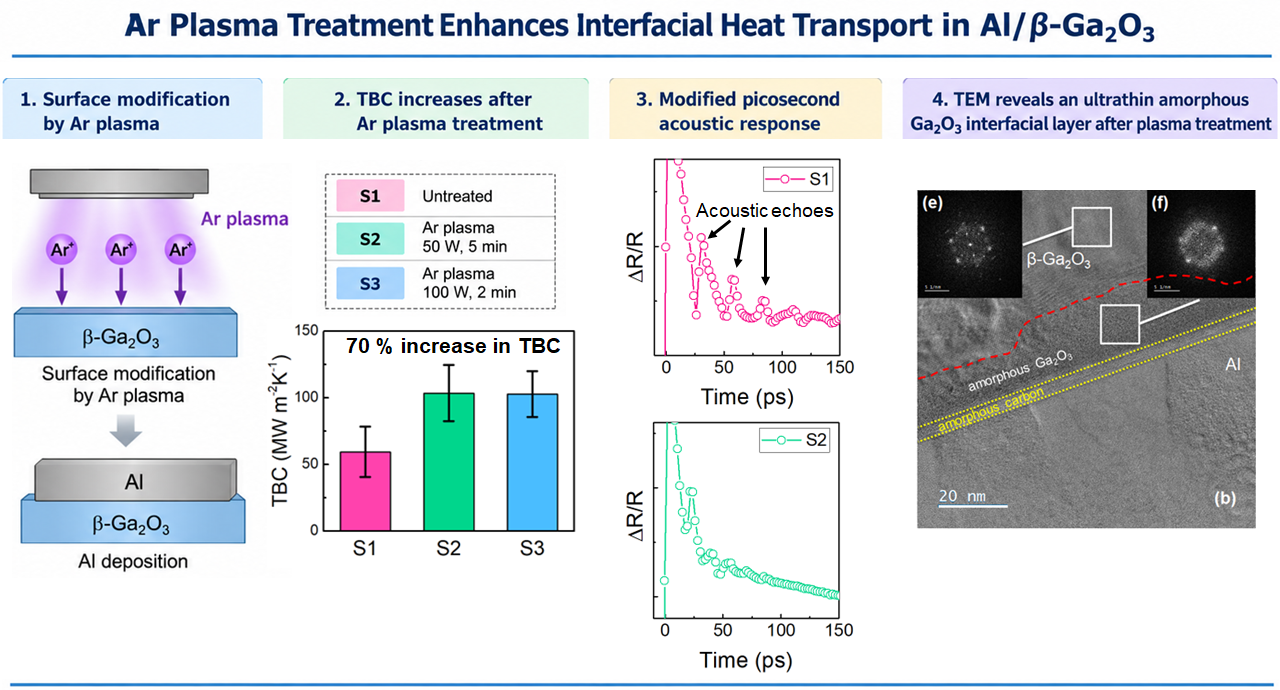
To investigate the effect of Ar plasma surface treatment on thermal transport across the Al/β-Ga₂O₃ interface, the thermal conductivity and TBC were measured for samples S1–S3, as shown in Figure 4. Sample S1 was left untreated, whereas S2 and S3 were exposed to Ar plasma at 50 W for 5 min and 100 W for 2 min, respectively. The measured β-Ga₂O₃ thermal conductivity varies only moderately among the three samples, remaining within approximately 5–7 W m⁻¹ K⁻¹. A pronounced change is observed in the Al/β-Ga₂O₃ TBC, as shown in Figure 4(b). The TBC increases from approximately 60 MW m⁻² K⁻¹ for the untreated S1 sample to about 100 MW m⁻² K⁻¹ for both plasma-treated samples, corresponding to an enhancement by approximately 70%. Picosecond acoustic measurements provide complementary information on the interfacial response as shown in Figure 4(c–e). The untreated S1 sample exhibits a pronounced sequence of coherent acoustic echoes following the initial response of the Al transducer, indicating repeated reflection of the acoustic strain pulse within the Al layer. In contrast, the higher-order echoes are strongly suppressed for the plasma-treated S2 and S3 samples, for which the acoustic response decays more rapidly after the first few oscillations. This clear difference demonstrates that Ar plasma treatment substantially modifies the acoustic response of the Al/β-Ga₂O₃ interface.
A qualitatively similar behavior was reported by Zheng et al., who observed considerably faster damping of acoustic echoes at Al/nonmetal interfaces exhibiting higher TBC and established a correlation between thermal conductance and acoustic transmission coefficient [21]. They attributed the enhancement primarily to stronger interfacial coupling resulting from surface-contamination removal and the formation of stronger interfacial bonds during surface treatment or sputter deposition. In their study, plasma pretreatment also increased the TBC of Al/Al₂O₃, Al/GaN, and Al/Si interfaces, supporting the general concept that modification of the nonmetal surface prior to Al deposition can substantially alter interfacial phonon transport.
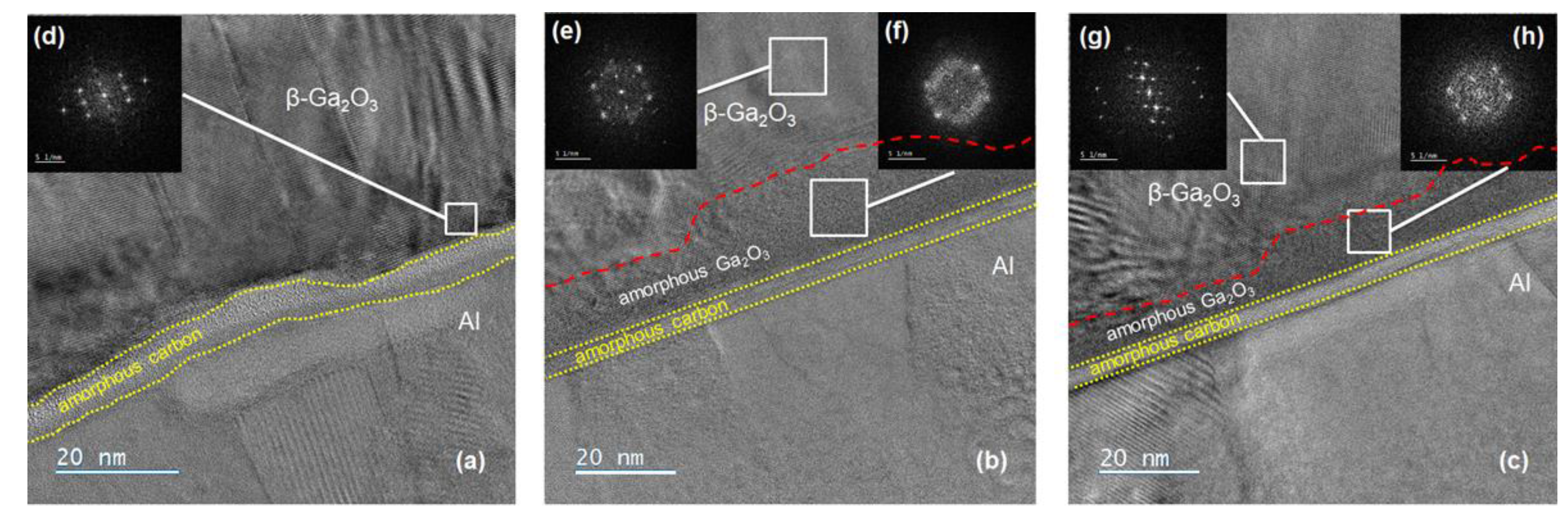
To clarify the structural origin of the plasma-induced change in TBC, the Al/β-Ga₂O₃ interfaces of S1–S3 were examined by cross-sectional HRTEM, as shown in Figure 5. The untreated S1 sample exhibits a comparatively abrupt transition between the crystalline β-Ga₂O₃ film and the interfacial region beneath the Al transducer. A thin carbon-containing layer is also present at the interface in all three samples, most likely originating from surface contamination prior to Al deposition. Since this layer is observed in both untreated and plasma-treated samples, its presence alone cannot account for the substantial difference in TBC. In contrast, both plasma-treated samples, S2 and S3, exhibit a thin partially amorphized region at the β-Ga₂O₃ surface directly beneath the Al layer. The corresponding FFTs from the indicated regions confirm that the underlying Ga₂O₃ film retains its crystalline β-phase after plasma treatment. Thus, the structural modification appears to be confined primarily to a thin near-surface region rather than extending throughout the film. This region is therefore attributed to near-surface structural modification induced by Ar plasma exposure.
4. Discussion
The formation of a thin partially amorphous Ga₂O₃ layer at the Al/β-Ga₂O₃ interface in S2 and S3, while the underlying film remains crystalline, demonstrates that Ar plasma treatment modifies the near-surface region governing interfacial heat transfer. This suggests that the enhancement may involve not only changes in interfacial bonding, but also the formation of an ultrathin transition region between Al and crystalline β-Ga₂O₃. Such a region may provide additional vibrational states that facilitate energy transfer across the interface by partially bridging the vibrational mismatch between the adjoining materials [33-38]. Several studies involving β-Ga₂O₃ support this possibility. Molecular dynamics simulations have shown that introducing a nanoscale SiO₂ interlayer between β-Ga₂O₃ and SiC can increase the TBC by up to 3.7 times, with the enhancement attributed to improved phonon spectral overlap, particularly in the low-frequency range, and an increased phonon participation ratio [33]. Similarly, in our previous calculations for β-Ga₂O₃/Si, we demonstrated that an ultrathin amorphous SiO₂ layer can act as a bridge between the vibrational modes of the two materials, with localized vibrational modes in the amorphous layer opening additional channels for thermal transport [23]. A related mechanism has recently been predicted for β-Ga₂O₃/Au interfaces, where oxygen-vacancy-induced disorder and interfacial mixing generate an alloy-like transition region that reduces the phonon mismatch and enhances interfacial heat transport [34]. Phonon-density-of-states analysis further showed enhanced overlap of low- and intermediate-frequency vibrational modes near the defective interface, providing additional pathways for phonon transmission [34]. More generally, theoretical studies of β-Ga₂O₃ interfaces containing two-dimensional interlayers have similarly shown that additional interfacial phonon modes can bridge the mismatch between the phonon spectra of adjoining materials and thereby increase TBC [35].
However, it should be emphasized that the presence of an amorphous or chemically modified interlayer does not universally enhance interfacial heat transport. Its effect depends strongly on the interlayer thickness, composition, bonding configuration, and vibrational properties. For example, in Ti/β-Ga₂O₃ interfaces, defective Ga₂O₃ together with a TiOx reaction layer was shown to introduce additional thermal resistance, with the low thermal conductivity of the oxide layer reducing the overall TBC [19]. Similarly, reaction-generated oxide layers at metal/β-Ga₂O₃ interfaces have been reported to lower TBC as their thickness increases [20]. These results demonstrate that a structurally disordered or chemically modified interfacial region can either facilitate or impede heat transfer depending on its specific characteristics. In the present samples, the observed enhancement therefore likely results from an ultrathin plasma-modified transition region that improves interfacial coupling without introducing sufficient additional thermal resistance to offset the increase in phonon transmission.
5. Conclusions
In this work, we investigated thermal transport in high-temperature RF-sputtered β-Ga₂O₃ thin films by combining advanced thermoreflectance techniques with structural, morphological, and microscopic characterization. The films exhibit a pronounced thickness-dependent thermal conductivity, increasing from approximately 5–7 W m⁻¹ K⁻¹ at 420 nm to about 10–12 W m⁻¹ K⁻¹ for thicker films. This evolution is accompanied by substantial micro-structural changes, including grain/domain coarsening and the development of intergranular void-like defects. The overall thickness dependence is reasonably described by a Debye–Klemens model incorporating boundary and defect-related phonon scattering, highlighting the important role of microstructure in governing heat transport in sputtered β-Ga₂O₃.
... We further demonstrate that thermal transport at the Al/β-Ga₂O₃ interface can be modified independently through Ar plasma treatment. Plasma exposure increases the thermal boundary conductance from approximately 60 to 100 MW m⁻² K⁻¹, corresponding to an enhancement of about 70%, while producing only a comparatively small change in the thermal conductivity of the underlying β-Ga₂O₃ film. The enhanced interfacial heat transfer is ac-companied by a pronounced modification of the picosecond acoustic response and the formation of an ultrathin amorphous/disordered near-surface region, while the underlying β-Ga₂O₃ remains crystalline. These observations indicate that plasma-induced modification of the near-surface structure and interfacial coupling plays an important role in the enhanced thermal boundary conductance.
Overall, the results demonstrate two complementary pathways for thermal-transport engineering in sputtered β-Ga₂O₃: film-scale control through thickness-dependent microstructural evolution and interface-scale control through plasma-induced surface modification. This provides a practical framework for tailoring both heat conduction within β-Ga₂O₃ layers and heat transfer across metal/β-Ga₂O₃ interfaces, with potential relevance to thermal management in β-Ga₂O₃-based power electronic devices.
Supplementary Materials
The Supplementary Materials include additional SEM and TEM characterization of the β-Ga₂O₃ films, as well as sensitivity analyses for the TDTR and FDTR measurements.
Author Contributions
Conceptualization, A.A. and K.S.; methodology, A.A. and K.S.; formal analysis, A.A., R.T., J.O.C. and K.S.; investigation, A.A., R.T., M.A.U., J.O.C. and A.M.I.; resources, M.A.U., A.M.I., Z.U; data curation, A.A. and R.T.; writing—original draft preparation, A.A.; writing—review and editing, A.A., J.O.C., K.S., Z.U.; visualization, A.A., R.T., J.O.C. and K.S.; supervision, Z.U.; project administration, A.A. and Z.U.; funding acquisition, K.S. and Z.U. All authors have read and agreed to the published version of the manuscript.
Funding
This work was supported by AP23489992 grant from the Science Committee of the Ministry of Science and Higher Education of the Republic of Kazakhstan. Additionally, this work was supported by the Nazarbayev University grants via Collaborative Research Program (CRP) [111024CRP2003 and 110326CRP0803], and Faculty Development Competitive Research Grants Program (FDCRGP) [20122022FD4130] in Kazakhstan.
Data Availability Statement
The data supporting the findings of this study are available from the corresponding author upon reasonable request.
Conflicts of Interest
The authors declare no conflicts of interest.
Abbreviations
The following abbreviations are used in this manuscript:
| UWBG | Ultrawide-bandgap |
| RF | Radio-frequency |
| TBC | Thermal boundary conductance |
| XRD | X-ray diffraction |
| AFM | Atomic force microscopy |
| HRTEM | High-resolution transmission electron microscopy |
| SEM | Scanning electron microscopy |
| TDTR | Time-domain thermoreflectance |
| FDTR | Frequency-domain thermoreflectance |
| BF-TEM | Bright-field transmission electron microscopy |
| PLD | Pulsed laser deposition |
| MBE | Molecular beam epitaxy |
| SAED | Selected-area electron diffraction |
| FFT | Fast Fourier Transform |
References
- Higashiwaki, M.; Jessen, G.H. Guest editorial: The dawn of gallium oxide microelectronics. Appl. Phys. Lett. 2018, 112, 060401. [Google Scholar] [CrossRef]
- Pearton, S.J.; Yang, J.; Cary, P.H., IV; Ren, F.; Kim, J.; Tadjer, M.J.; Mastro, M.A. A review of Ga₂O₃ materials, processing, and devices. Appl. Phys. Rev. 2018, 5, 011301. [Google Scholar] [CrossRef]
- Baldini, M.; Galazka, Z.; Wagner, G. Recent progress in the growth of β-Ga₂O₃ for power electronics applications. Mater. Sci. Semicond. Process. 2018, 78, 132–146. [Google Scholar] [CrossRef]
- Guo, Z.; Verma, A.; Wu, X.; Sun, F.; Hickman, A.; Masui, T.; Kuramata, A.; Higashiwaki, M.; Jena, D.; Luo, T. Anisotropic thermal conductivity in single-crystal β-gallium oxide. Appl. Phys. Lett. 2015, 106, 111909. [Google Scholar] [CrossRef]
- Jiang, P.; Qian, X.; Li, X.; Yang, R. Three-dimensional anisotropic thermal conductivity tensor of single-crystalline β-Ga₂O₃. Appl. Phys. Lett. 2018, 113, 232105. [Google Scholar] [CrossRef]
- Santia, M.D.; Tandon, N.; Albrecht, J.D. Lattice thermal conductivity in β-Ga₂O₃ from first principles. Appl. Phys. Lett. 2015, 107, 041907. [Google Scholar] [CrossRef]
- Chatterjee, C.; Zeng, K.; Nordquist, C.D.; Singisetti, U.; Choi, S. Device-level thermal management of gallium oxide field-effect transistors. IEEE Trans. Compon. Packag. Manuf. Technol. 2019, 9, 2352–2365. [Google Scholar] [CrossRef]
- Yuan, C.; Zhang, Y.; Montgomery, R.; Kim, S.; Shi, J.; Mauze, A.; Itoh, T.; Speck, J.S.; Graham, S. Modeling and analysis for thermal management in gallium oxide field-effect transistors. J. Appl. Phys. 2020, 127, 154502. [Google Scholar] [CrossRef]
- Cheng, Z.; Mu, F.; You, T.; Xu, W.; Shi, J.; Liao, M.E.; Wang, Y.; Huynh, K.; Suga, T.; Goorsky, M.S.; et al. Thermal transport across ion-cut monocrystalline β-Ga₂O₃ thin films and bonded β-Ga₂O₃–SiC interfaces. ACS Appl. Mater. Interfaces 2020, 12, 44943–44951. [Google Scholar] [CrossRef] [PubMed]
- Szwejkowski, C.J.; Creange, N.C.; Sun, K.; Giri, A.; Donovan, B.F.; Constantin, C.; Hopkins, P.E. Size effects in the thermal conductivity of gallium oxide (β-Ga₂O₃) films grown via open-atmosphere annealing of gallium nitride. J. Appl. Phys. 2015, 117, 084308. [Google Scholar] [CrossRef]
- Blumenschein, N.; Slomski, M.; Paskov, P.P.; Kaess, F.; Breckenridge, M.H.; Muth, J.F.; Paskova, T. Thermal conductivity of bulk and thin-film β-Ga₂O₃ measured by the 3ω technique. Proc. SPIE 2018, 10533, 105332G. [Google Scholar]
- Zhang, Y.; Su, Q.; Zhu, J.; Koirala, S.; Koester, S.J.; Wang, X. Thickness-dependent thermal conductivity of mechanically exfoliated β-Ga₂O₃ thin films. Appl. Phys. Lett. 2020, 116, 202101. [Google Scholar] [CrossRef]
- Vaca, D.; Barry, M.; Yates, L.; Nepal, N.; Katzer, D.S.; Downey, B.P.; Wheeler, V.D.; Nyakiti, L.O.; Meyer, D.J.; Graham, S.; et al. Measurements and numerical calculations of thermal conductivity to evaluate the quality of β-gallium oxide thin films grown on sapphire and silicon carbide by molecular beam epitaxy. Appl. Phys. Lett. 2022, 121, 042107. [Google Scholar] [CrossRef]
- Song, Y.; Ranga, P.; Zhang, Y.; Feng, Z.; Huang, H.-L.; Santia, M.D.; Badescu, S.C.; Gonzalez-Valle, C.U.; Perez, C.; Ferri, K.; et al. Thermal conductivity of β-phase Ga₂O₃ and (AlₓGa₁₋ₓ)₂O₃ heteroepitaxial thin films. ACS Appl. Mater. Interfaces 2021, 13, 38477–38490. [Google Scholar] [CrossRef] [PubMed]
- Saikumar, A.K.; Nehate, S.D.; Sundaram, K.B. Review—RF sputtered films of Ga₂O₃. ECS J. Solid State Sci. Technol. 2019, 8, Q3064–Q3078. [Google Scholar] [CrossRef]
- Guo, Z.; Mao, Y. Optimization of Ga₂O₃ thin-film growth via magnetron sputtering: Influence of growth pressure on crystallinity, surface morphology, and optical properties. Vacuum 2025, 234, 114057. [Google Scholar] [CrossRef]
- Sharma, S.; Nagib, H.; Le, P.Y.; Allen, M.W.; Holland, A.S.; Partridge, J.G.; Tran, H.N. Structural, surface, electrical and UVC sensing properties of high-temperature RF-sputtered gallium oxide thin films. Mater. Today Electron. 2025, 11, 100139. [Google Scholar] [CrossRef]
- Ismailov, A.M.; Umakhanov, M.A.; Rabadanov, M.R.; Rabadanov, M.Kh. Epitaxial deposition of β-Ga₂O₃ films by radio-frequency magnetron sputtering at elevated substrate temperatures. Vacuum 2026, 244, 114840. [Google Scholar] [CrossRef]
- Shi, J.; Yuan, C.; Huang, H.-L.; Johnson, J.; Chae, C.; Wang, S.; Hanus, R.; Kim, S.; Cheng, Z.; Hwang, J.; et al. Thermal transport across metal/β-Ga₂O₃ interfaces. ACS Appl. Mater. Interfaces 2021, 13, 29083–29091. [Google Scholar] [CrossRef] [PubMed]
- Aller, H.T.; Yu, X.; Wise, A.; Howell, R.S.; Gellman, A.J.; McGaughey, A.J.H.; Malen, J.A. Chemical reactions impede thermal transport across metal/β-Ga₂O₃ interfaces. Nano Lett. 2019, 19, 8533–8538. [Google Scholar] [CrossRef] [PubMed]
- Zheng, W.; Miao, Z.; Zhou, X.; Li, G.; Wu, H.; Wei, J.; Li, H. Effectively tuning phonon transport across Al/nonmetal interfaces through controlling interfacial bonding strength without modifying thermal conductivity. Mater. Today Phys. 2025, 52, 101676. [Google Scholar] [CrossRef]
- Jiang, P.; Qian, X.; Yang, R. Tutorial: Time-domain thermoreflectance (TDTR) for thermal property characterization of bulk and thin-film materials. J. Appl. Phys. 2018, 124, 161103. [Google Scholar] [CrossRef]
- Abdullaev, A.; Mukhangaliyeva, L.; Sekerbayev, K.; Esteves, D.M.; Pedro, M.C.; Alves, L.C.; Lorenz, K.; Peres, M.; Utegulov, Z. Thermal transport in ion-beam-exfoliated β-Ga₂O₃ nanomembranes. APL Mater. 2025, 13, 051120. [Google Scholar] [CrossRef]
- Kurbanova, B.; Chakraborty, D.; Abdullaev, A.; Shamatova, A.; Makukha, O.; Belarouci, A.; Lysenko, V.; Azarov, A.; Kuznetsov, A.; Wang, Y.; et al. Multiscale phonon thermal transport in nano-porous silicon. Appl. Phys. Lett. 2024, 124, 252202. [Google Scholar] [CrossRef]
- Shamatova, A.; Abdullaev, A.; O’Connell, J.; Kušnír, J.; Grabec, T.; Sekerbayev, K.; Skuratov, V.; Utegulov, Z. Anisotropic thermal transport in robust crystalline yttrium aluminium garnet tunable by long oriented amorphous nano-tracks. Int. J. Therm. Sci. 2026, 222, 110583. [Google Scholar] [CrossRef]
- Cahill, D.G. Analysis of heat flow in layered structures for time-domain thermoreflectance. Rev. Sci. Instrum. 2004, 75, 5119–5122. [Google Scholar] [CrossRef]
- Schmidt, A.J.; Cheaito, R.; Chiesa, M. A frequency-domain thermoreflectance method for the characterization of thermal properties. Rev. Sci. Instrum. 2009, 80, 094901. [Google Scholar] [CrossRef] [PubMed]
- Tritt, T.M. (Ed.) Thermal Conductivity: Theory, Properties, and Applications; Springer: New York, NY, USA, 2004. [Google Scholar]
- Tran, D.Q.; Blumenschein, N.; Mock, A.; Sukkaew, P.; Zhang, H.; Muth, J.F.; Paskova, T.; Paskov, P.P.; Darakchieva, V. Thermal conductivity of ultra-wide bandgap thin layers—High Al-content AlGaN and β-Ga₂O₃. Phys. B Condens. Matter 2020, 579, 411810. [Google Scholar] [CrossRef]
- Tadjer, M.J.; Mastro, M.A.; Mahadik, N.A.; Currie, M.; Wheeler, V.D.; Freitas, J.A.; Greenlee, J.D.; Hite, J.K.; Hobart, K.D.; Eddy, C.R.; et al. Structural, optical, and electrical characterization of monoclinic β-Ga₂O₃ grown by MOVPE on sapphire substrates. J. Electron. Mater. 2016, 45, 2031–2037. [Google Scholar] [CrossRef]
- Kranert, C.; Sturm, C.; Schmidt-Grund, R.; Grundmann, M. Raman tensor elements of β-Ga₂O₃. Sci. Rep. 2016, 6, 35964. [Google Scholar] [CrossRef] [PubMed]
- Dong, S.; Zhang, G.; Guo, L.; Xin, Q.; Wang, X.; Xin, G. Exploring thermal transport in β-Ga₂O₃ films: The effect of epitaxial growth parameters. Ceram. Int. 2026, 52, 28096–28107. [Google Scholar] [CrossRef]
- Li, Y.; Sun, F. Thermal boundary conductance in heterogeneous integration between β-Ga₂O₃ and semiconductors. Ceram. Int. 2024, 50, 18787–18796. [Google Scholar] [CrossRef]
- Wang, B.; Wang, B.; Yan, H.; Cai, Y. Oxygen vacancy-driven interfacial alloying and mixing for enhanced heat transfer in gallium oxide. Mater. Today Phys. 2025, 54, 101714. [Google Scholar] [CrossRef]
- Makumi, S.W.; Akšamija, Z. 2D materials enhance thermal conductance at van der Waals interfaces of β-Ga₂O₃. J. Phys. Chem. C 2026, 130, 9879–9887. [Google Scholar] [CrossRef]
- Xu, B.; Mu, F.; Liu, Y.; Guo, R.; Hu, S.; Shiomi, J. Record-low thermal boundary resistance at bonded GaN/diamond interface by controlling ultrathin heterogeneous amorphous layer. Acta Mater. 2025, 282, 120458. [Google Scholar] [CrossRef]
- Shen, Y.; Qi, X.; Li, Y.; Guo, Y.; Huang, Q.; Dai, W.; Yuan, Q.; Gu, L.; Ding, C.; Chen, W.-J.; et al. Improving interfacial thermal conductivity by constructing covalent bond between Ga₂O₃ and SiC. Nat. Commun. 2025, 16, 10723. [Google Scholar] [CrossRef] [PubMed]
- Li, H.; Wu, H.; Zhai, D.; Lu, J. Structural evolution of amorphous SiO₂ and its impact on interfacial heat transport with β-Ga₂O₃. J. Non-Cryst. Solids 2026, 688, 124168. [Google Scholar] [CrossRef]
Figure 1.
Structural characterization of RF-sputtered β-Ga₂O₃ films with different thicknesses. Cross-sectional bright-field transmission electron microscopy (BF-TEM) images of the (a) 420 nm, (b) 1100 nm, and (c) 2100 nm films. (d) X-ray diffraction (XRD) patterns of the same β-Ga₂O₃ films, where reflections originating from the c-Al₂O₃ substrate are also indicated. (e) Raman spectra of the corresponding films. Blue and red dashed lines mark the characteristic Ag and Bg Raman modes of monoclinic β-Ga₂O₃, respectively, while asterisks denote Raman features originating from the sapphire substrate.
Figure 1.
Structural characterization of RF-sputtered β-Ga₂O₃ films with different thicknesses. Cross-sectional bright-field transmission electron microscopy (BF-TEM) images of the (a) 420 nm, (b) 1100 nm, and (c) 2100 nm films. (d) X-ray diffraction (XRD) patterns of the same β-Ga₂O₃ films, where reflections originating from the c-Al₂O₃ substrate are also indicated. (e) Raman spectra of the corresponding films. Blue and red dashed lines mark the characteristic Ag and Bg Raman modes of monoclinic β-Ga₂O₃, respectively, while asterisks denote Raman features originating from the sapphire substrate.
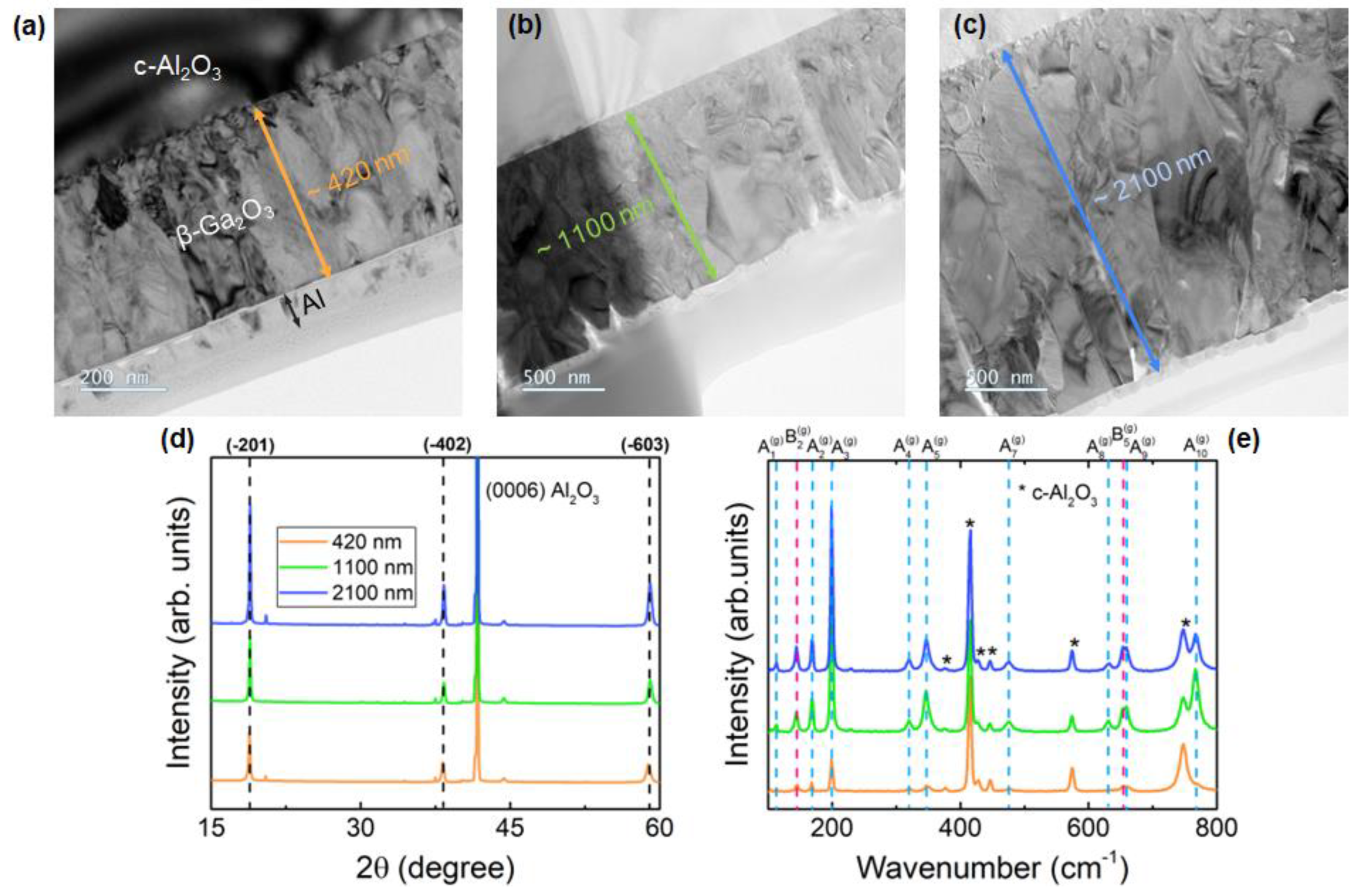
Figure 2.
Surface morphology of RF-sputtered β-Ga₂O₃ films with thicknesses of (a) 420 nm, (b) 1100 nm, and (c) 2100 nm measured by AFM. All topographic maps were acquired over an area of 10×10 μm².
Figure 2.
Surface morphology of RF-sputtered β-Ga₂O₃ films with thicknesses of (a) 420 nm, (b) 1100 nm, and (c) 2100 nm measured by AFM. All topographic maps were acquired over an area of 10×10 μm².
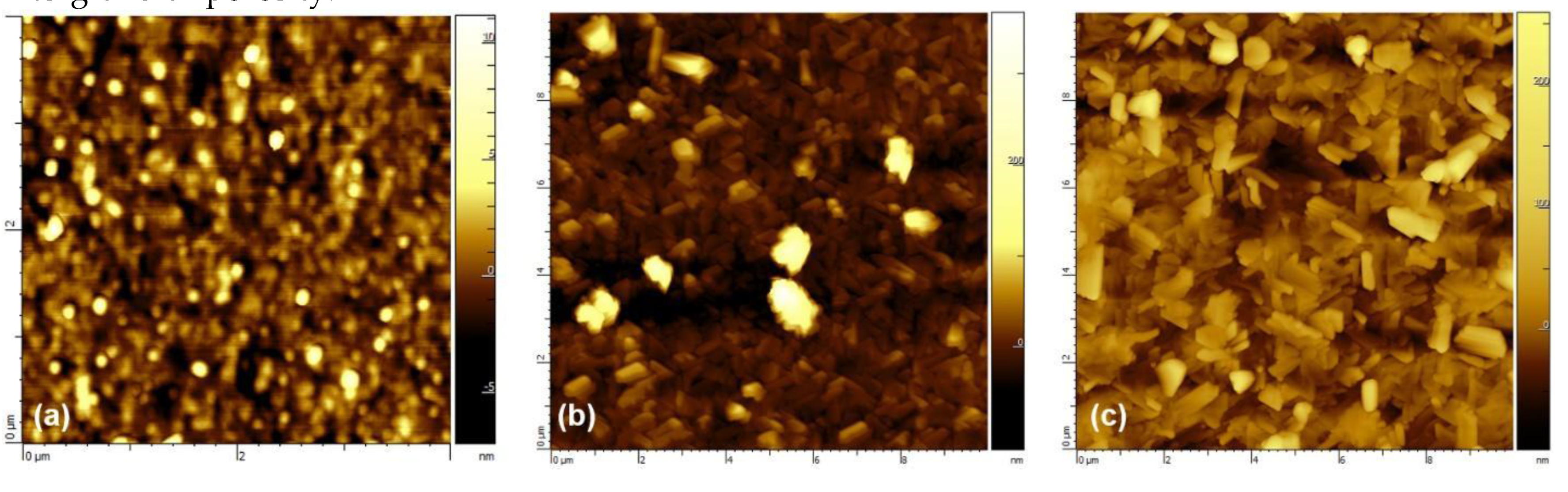
Figure 3.
Thickness-dependent thermal transport in RF-sputtered β-Ga₂O₃ films. (a) Representative TDTR signals and (b) FDTR phase responses for films of different thicknesses. Open circles represent the experimental data, while black solid lines show the corresponding fits obtained using the multilayer heat-diffusion model. (c) Thermal conductivity as a function of β-Ga₂O₃ film thickness. Solid symbols represent the thermal conductivities obtained in the present work by TDTR and FDTR, whereas open symbols show literature values reported for β-Ga₂O₃ thin films fabricated using different approaches [11-14, 23, 31]. The solid line represents the semi-analytical Debye-model calculation described by Eq. (1), and the black dashed line indicates the literature bulk thermal conductivity of β-Ga₂O₃ for the (−201) orientation [4].
Figure 3.
Thickness-dependent thermal transport in RF-sputtered β-Ga₂O₃ films. (a) Representative TDTR signals and (b) FDTR phase responses for films of different thicknesses. Open circles represent the experimental data, while black solid lines show the corresponding fits obtained using the multilayer heat-diffusion model. (c) Thermal conductivity as a function of β-Ga₂O₃ film thickness. Solid symbols represent the thermal conductivities obtained in the present work by TDTR and FDTR, whereas open symbols show literature values reported for β-Ga₂O₃ thin films fabricated using different approaches [11-14, 23, 31]. The solid line represents the semi-analytical Debye-model calculation described by Eq. (1), and the black dashed line indicates the literature bulk thermal conductivity of β-Ga₂O₃ for the (−201) orientation [4].
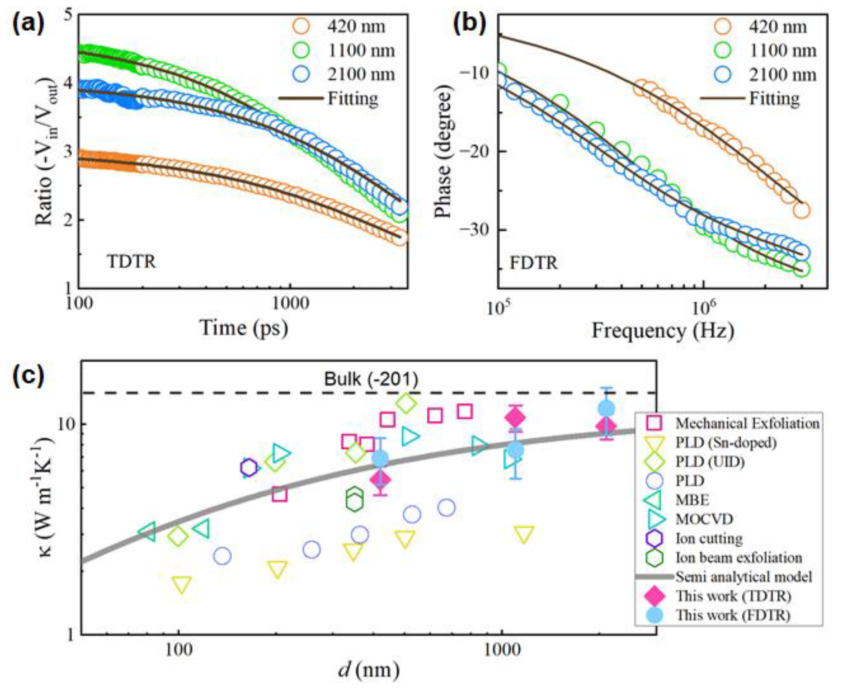
Figure 4.
Effect of Ar plasma surface treatment on thermal transport across the Al/β-Ga₂O₃ interface. (a) Thermal conductivity of the β-Ga₂O₃ films and (b) thermal boundary conductance (TBC) of the Al/β-Ga₂O₃ interface for samples S1–S3. S1 corresponds to the untreated sample, whereas S2 and S3 were exposed to Ar plasma at 50 W for 5 min and 100 W for 2 min, respectively. (c–e) Corresponding picosecond acoustic signals measured for (c) S1, (d) S2, and (e) S3.
Figure 4.
Effect of Ar plasma surface treatment on thermal transport across the Al/β-Ga₂O₃ interface. (a) Thermal conductivity of the β-Ga₂O₃ films and (b) thermal boundary conductance (TBC) of the Al/β-Ga₂O₃ interface for samples S1–S3. S1 corresponds to the untreated sample, whereas S2 and S3 were exposed to Ar plasma at 50 W for 5 min and 100 W for 2 min, respectively. (c–e) Corresponding picosecond acoustic signals measured for (c) S1, (d) S2, and (e) S3.
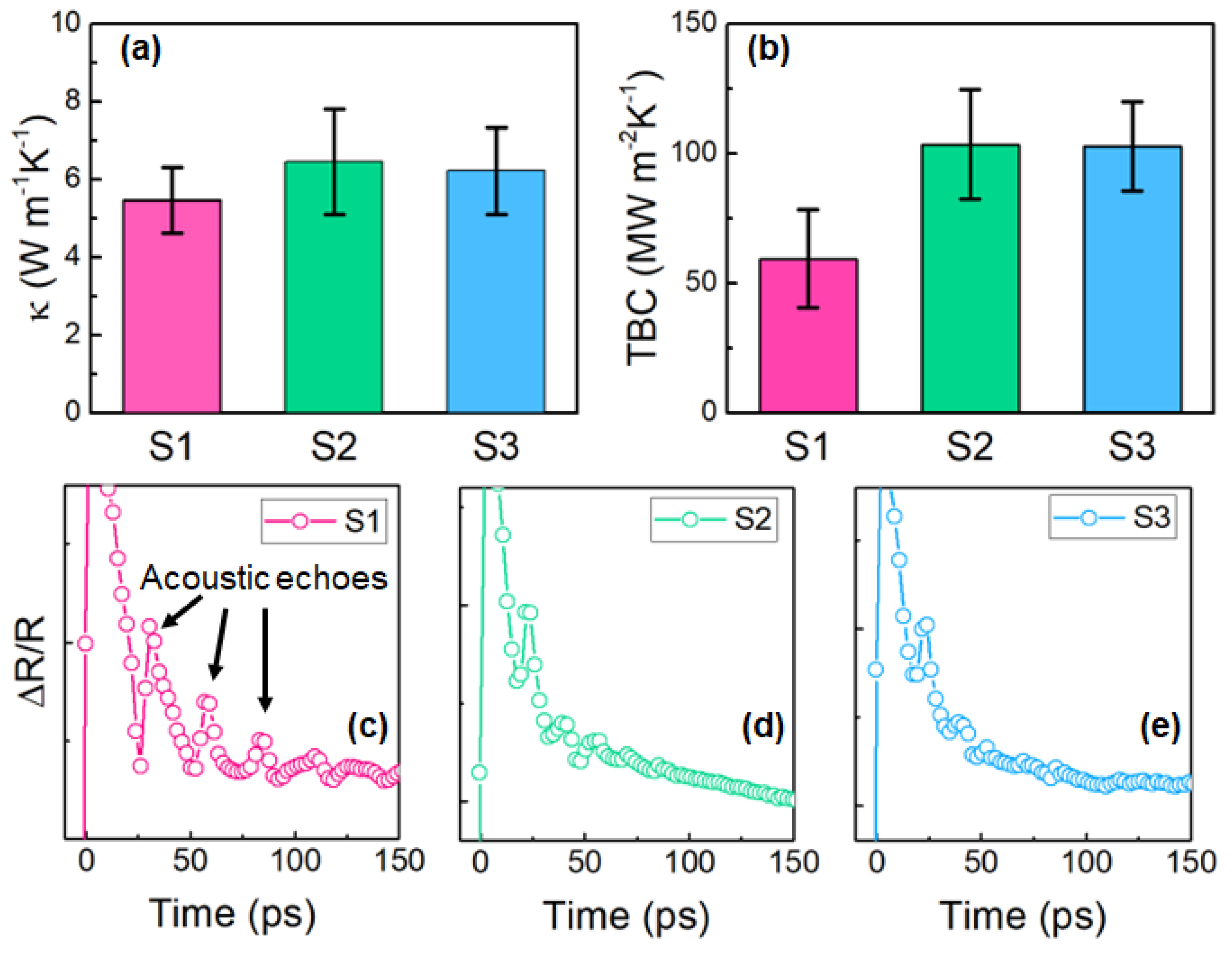
Figure 5.
Cross-sectional TEM characterization of the Al/β-Ga₂O₃ interfaces without and with Ar plasma treatment. High-resolution BF-TEM images of (a) untreated S1, (b) S2 treated at 50 W for 5 min, and (c) S3 treated at 100 W for 2 min. (d–h) Selected-area electron diffraction (SAED) patterns acquired from the regions indicated by the white squares in panels (a–c). Yellow dotted lines mark the amorphous carbon-containing surface-contamination layer observed at the interfaces, whereas the red dashed lines in panels (b) and (c) define the plasma-induced amorphous/disordered Ga₂O₃ region. The corresponding SAED patterns confirm the structural differences between the crystalline β-Ga₂O₃ film and the disordered interfacial regions.
Figure 5.
Cross-sectional TEM characterization of the Al/β-Ga₂O₃ interfaces without and with Ar plasma treatment. High-resolution BF-TEM images of (a) untreated S1, (b) S2 treated at 50 W for 5 min, and (c) S3 treated at 100 W for 2 min. (d–h) Selected-area electron diffraction (SAED) patterns acquired from the regions indicated by the white squares in panels (a–c). Yellow dotted lines mark the amorphous carbon-containing surface-contamination layer observed at the interfaces, whereas the red dashed lines in panels (b) and (c) define the plasma-induced amorphous/disordered Ga₂O₃ region. The corresponding SAED patterns confirm the structural differences between the crystalline β-Ga₂O₃ film and the disordered interfacial regions.

Disclaimer/Publisher’s Note: The statements, opinions and data contained in all publications are solely those of the individual author(s) and contributor(s) and not of MDPI and/or the editor(s). MDPI and/or the editor(s) disclaim responsibility for any injury to people or property resulting from any ideas, methods, instructions or products referred to in the content. |
© 2026 by the authors. Licensee MDPI, Basel, Switzerland. This article is an open access article distributed under the terms and conditions of the Creative Commons Attribution (CC BY) license (http://creativecommons.org/licenses/by/4.0/).
Copyright: This open access article is published under a Creative Commons CC BY 4.0 license, which permit the free download, distribution, and reuse, provided that the author and preprint are cited in any reuse.