

Submitted:
30 September 2026
Posted:
02 October 2026
You are already at the latest version
Abstract
Wearable bioimpedance spectroscopy within Internet of Medical Things ecosystems requires energy-efficient analog front-ends (AFEs) capable of processing small impedance-dependent signals over a wide excitation-frequency range. This paper presents a preliminary study of an automated gm/ID-based framework for the co-design of wideband CMOS instrumentation amplifiers, jointly considering power, noise, bandwidth, and frequency-dependent common-mode rejection. The proposed flow combines technology-characterized device data, Verilog-A behavioral modeling, Python-based optimization, and SKILL-assisted transistor-level verification. The methodology is applied to a wideband CMOS current-feedback instrumentation amplifier (CFIA) designed in a 180-nm CMOS technology. Operating from a 1.8-V supply, the amplifier provides a nominal gain of 30 V/V over the 1-kHz to 2-MHz signal band. Particular attention is given to the coupling between transistor sizing, parasitic capacitance, and high-frequency CMRR in a local current-feedback topology. The paper establishes the BIS readout requirements, describes the selected CFIA architecture, and formulates the main design variables and optimization targets. The presented results constitute the initial stage of a broader design framework; complete optimization, statistical robustness, and experimental validation are reserved for the subsequent full study.
Keywords:
CMOS instrumentation amplifier
; current-feedback instrumentation amplifier
; analog design automation
; bioimpedance spectroscopy
; gm/ID methodology
; multi-objective optimization
I. Introduction
The integration of sensing, communication, and data-processing capabilities into Internet of Medical Things platforms is enabling distributed and continuous monitoring of physiological and biological variables. Wearable devices are particularly attractive for this purpose, but their limited power budget, physical dimensions, and thermal constraints impose stringent requirements on the associated analog front-end [1,2,3].
Bioelectric impedance, commonly referred to as bioimpedance, has emerged as a promising technique for both personal and clinical wearable devices. Depending on the measurement configuration and operating frequency, bioimpedance can provide information associated with respiratory activity, body-fluid variations, and other physiological parameters [4,5]. In contrast to single-frequency measurements, bioimpedance spectroscopy (BIS) characterizes the complex impedance over a range of excitation frequencies. Although many bioimpedance applications operate below a few hundred kilohertz, wideband implementations extending to approximately 1 MHz have also been reported [11]. This broadband operation places stringent requirements on the analog signal-processing circuitry used to acquire the impedance-dependent voltage.
In a BIS interface, low-level impedance-dependent voltage variations must be acquired in the presence of electrode-tissue effects, common-mode interference, electronic noise, and potentially large static impedance components [8,9]. Although every block in the readout chain affects the final impedance accuracy, this work focuses on the instrumentation amplifier (IA), whose frequency response, noise, and common-mode rejection directly affect the accuracy of the subsequent impedance demodulation process.
Current-feedback instrumentation amplifiers (CFIAs) are attractive for this application because they can combine high input impedance, defined closed-loop gain, and wideband operation [6,7]. However, their high-frequency common-mode rejection ratio (CMRR) can be affected by asymmetric internal signal paths and unequal parasitic capacitances. In current-mirror-loaded implementations, transistor dimensions and circuit topology determine the parasitic loading of internal nodes. At high frequency, differences between these paths can introduce common-mode-to-differential conversion and consequently limit the achievable CMRR [7]
These interactions make the design of a low-power wideband CFIA a multidimensional problem. Transistor operating points and dimensions simultaneously affect transconductance efficiency, bias current, intrinsic gain, bandwidth, noise, mismatch, and parasitic capacitance. A design procedure based only on nominal schematic-level simulations may require extensive manual iteration and may not provide adequate robustness when process and mismatch effects are considered.
The gm/ID methodology provides provides a systematic basis for exploring these device-level trade-offs through technology-characterized transistor data [10]. This methodology is particularly attractive for energy-constrained AFEs, where power efficiency cannot be optimized independently of bandwidth, noise, linearity, and robustness. Nevertheless, the design of a wideband CFIA with parasitic-sensitive high-frequency CMRR requires more than conventional gm/ID-based transistor sizing. The designer must establish a connection between circuit specifications, device-level design variables, frequency-dependent circuit behavior, and transistor-level verification under process and mismatch variations. This motivates an automated co-design approach in which different abstraction levels are combined within a single optimization flow.
This work therefore investigates an automated gm/ID-based co-design framework for wideband CMOS CFIAs intended for BIS readout interfaces. The approach combines technology-characterized device data, Verilog-A behavioral modeling, Python-based optimization, and Cadence Virtuoso/SKILL automation. The preliminary study focuses on a 180-nm CMOS CFIA operating from a 1.8-V supply and targeting a nominal gain of 30 V/V.
The main contributions of this preliminary study are: 1) formulation of a specification-driven gm/ID-based design methodology for a wideband CFIA; 2) integration of device characterization, behavioral modeling, and EDA automation into a common design flow; and 3) identification of the coupling between transistor sizing, parasitic capacitance, high-frequency CMRR, power consumption, input-referred noise, bandwidth as a key design consideration.
The remainder of the paper is organized as follows. Section II describes the BIS readout architecture and derives the relevant IA requirements. Section III presents the selected CFIA topology and its frequency-dependent behavior. Section IV introduces the preliminary gm/ID-based co-design framework. Section V discusses the status and limitations of the study.
II. BIS Readout Architecture and Design Requirements
A. Bioimpedance Spectroscopy Readout Architecture
A typical monolithic BIS interface converts the electrical impedance of the medium under test (MUT), denoted as ZX, into an electrical signal through a controlled excitation current and subsequently extracts the impedance information using analog signal-conditioning and demodulation circuits. A simplified four-electrode BIS architecture is shown in Figure 1. [9]. The excitation current generator (CG) injects a sinusoidal current into the MUT, producing an impedance-dependent voltage that is acquired by the voltage readout path. The IA amplifies this voltage, while the demodulator extracts the corresponding impedance information before digitization by an analog-to-digital converter (ADC).
The four-electrode configuration separates the current-injection path from the voltage-sensing path. This arrangement is particularly suitable for precision bioimpedance measurements because the high input impedance of the IA minimizes the current flowing through the electrode-tissue impedance and consequently reduces the associated voltage drop. The distinction between two- and four-electrode configurations and the importance of IA input impedance are discussed in detail in [8].
The voltage-readout architecture considered in this work employs polar demodulation, as illustrated in Figure 2. The MUT and reference resistor RS are excited by the same current, producing voltages VZ and VS, respectively. These signals are amplified by two IAs and, thus, yield two voltage signals, VAZ and VAS, which are then processed by magnitude and phase detectors to obtain two DC voltages, Vm and Vp, proportional to the magnitude and phase of ZX. The use of RS provides a ratiometric measurement and reduces first-order sensitivity to excitation-current amplitude. However, residual gain, phase, CMRR, noise, nonlinearity, and channel mismatch between the two IA paths directly affect the estimated impedance. The IA specifications must therefore be derived from an end-to-end impedance-error budget instead of being selected independently at circuit level.
Because the two amplification paths form part of a ratiometric measurement, mismatch in gain and phase response between the two IAs can introduce errors in the extracted impedance magnitude and phase. The IA requirements considered in this work are therefore summarized in Table 1.
B. Instrumentation Amplifier Requirements for the BIS Readout
The system-level requirements of the BIS interface are translated into the corresponding IA-level specifications. The IA must provide sufficiently high input impedance to minimize loading of the voltage-sensing electrodes, low input-referred noise to preserve impedance sensitivity, adequate differential-mode linearity and output swing to accommodate the measured signal, and sufficient CMRR to suppress common-mode interference over the excitation band [8,9].
The specifications in Table 1 are coupled at the transistor level. The input-stage transconductance affects both bandwidth and input-referred thermal noise, while bias current directly determines power consumption. Device dimensions influence matching and intrinsic gain but also modify parasitic capacitances. In the selected CFIA topology, these dependencies additionally affect high-frequency CMRR. The resulting coupled design space motivates the proposed automated co-design methodology.
III. Local Current-Feedback Instrumentation Amplifier
A) Architecture
To satisfy the requirements summarized in Table 1, a CMOS current-feedback instrumentation amplifier (CFIA) is considered. The topology, shown in Figure 3, employs separate feedback loops around the input and output transconducting stages. The input stage converts the differential input voltage into signal currents, while the output stage converts the feedback current into the output voltage. Separating the two feedback loops avoids stacking the input and output transconductors in the main signal path and therefore facilitates low-voltage operation and independent control of the two transconductances.
The topology is particularly suitable for the present study because its frequency response is determined not only by the nominal transconductances and feedback resistors but also by the internal high-impedance nodes associated with current mirrors and feedback amplifiers. These nodes introduce parasitic poles and frequency-dependent imbalance that can become relevant to the CMRR at the upper end of the operating band.
B) Transistor-level implementation
Figure 4 shows the transistor-level implementation adopted in this study. The input stage is based on a resistively degenerated differential transconductor, while the output stage incorporates the corresponding current-feedback loop. The input section provides high input impedance and converts the differential input voltage into signal currents. The output section reproduces these currents through the local feedback loop and develops the required output voltage.
Under the low-frequency operating conditions of the local feedback loops, the nominal closed-loop gain can be expressed as
where ki is the nominal current-transfer ratio, which is approximately unity for the considered implementation, and Gm,in and Gm,out denote the effective transconductances of the input and output stages, respectively. Equation (1) is used here as a low-frequency design relation; the complete frequency-dependent gain also depends on the internal transistor dynamics and parasitic capacitances.
C) High-frequency CMRR
The internal current-mirror nodes are particularly relevant to the high-frequency common-mode response. Because corresponding nodes are connected to different transistor structures, their small-signal impedances and total parasitic capacitances are not necessarily identical. The latter depends on the transistor dimensions and operating points through the intrinsic device capacitances, including and , as well as on interconnect parasitics. Let and denote the equivalent capacitances associated with two relevant internal nodes. Under common-mode excitation, the corresponding capacitive currents are:
Any imbalance between these currents produces a residual differential internal signal. Since the parasitic capacitances depend on transistor dimensions and operating points, the high-frequency CMRR becomes coupled to the transistor sizing problem. This dependency motivates the inclusion of frequency-dependent CMRR in the proposed co-design methodology gm/ID-based co-design methodology.
IV. Preliminary gm/ID-Based Co-Design Methodology
The proposed methodology establishes a specification-driven flow from the BIS requirements to transistor-level CFIA sizing. The approach combines technology-characterized device data, behavioral modeling, numerical optimization, and circuit-level verification.
First, the 180-nm CMOS technology is characterized through simulations to obtain the relevant gm/ID relationships and device parameters as functions of bias and transistor dimensions. The main design variables are the gm/ID ratios, channel lengths, and bias currents of the input and output transconducting stages, together with the dimensions of devices that dominate the internal parasitic capacitances. The transistor widths are subsequently determined from the corresponding current-density data.
The circuit specifications in Table 1 are then translated into constraints on gain, bandwidth, noise, power consumption, and high-frequency CMRR. In particular, the nominal closed-loop gain provides a first-order constraint on the ratio between the effective input and output transconductances.
V. Discussion and Limitations
This preliminary study establishes the system-to-circuit design framework and identifies the principal coupling mechanisms relevant to automated wideband CFIA sizing. In particular, the analysis shows that the requirements of a BIS voltage-readout stage cannot be translated into independent transistor-level constraints because bandwidth, noise, power consumption, and high-frequency CMRR are coupled through transistor operating conditions, device dimensions, and parasitic capacitances.
At the current stage, the complete optimization flow has not yet been quantitatively evaluated over the full design space. Likewise, statistical PVT and mismatch results, post-layout verification, and experimental measurements are not included in this preliminary version. These analyses are part of the ongoing development of the complete methodology. The final objective weighting, numerical specification limits, and optimization results will also depend on the complete end-to-end BIS error budget.
The purpose of this preprint is therefore to document the initial formulation of the proposed methodology and its circuit-level rationale. The subsequent full study will provide quantitative optimization results, transistor-level verification, statistical analysis, and experimental validation.
Acknowledgments
This research was funded in part by Junta de Extremadura (Spain), grant number IDA3-23-0001-3.
References
- G.R. Pradyumna, et al., "Empowering healthcare with IoMT: evolution, machine learning integration, security, and interoperability challenges," IEEE Access, vol. 12, pp. 20603-20623, 2024. [CrossRef]
- G. Huang, X. Chen, and C. Liao, "AI-Driven wearable bioelectronics in digital healthcare," Biosensors 15, no. 7: 410. 2025. [CrossRef]
- D. Kilani, B. Mohammad, M. Alhawari, H. Saleh, and M. Ismail, Power Management for Wearable Electronic Devices, Analog Circuits and Signal Processing, Springer International Publishing, 2020.
- N. Arabsalmani, et al, “Exploring bio-impedance sensing for intelligent wearable devices,” Bioengineering 12, no. 5: 521. 2025. [CrossRef]
- W. Groenendaal, S. Lee, and C. van Hoof, “Wearable bioimpedance monitoring: viewpoint for application in chronic conditions,” JMIR Biomed. Eng., vol. 6, Apr. – Jun. 2021. [CrossRef]
- Corbacho, J.M. Carrillo, J.L. Ausín, M.Á. Domínguez, R. Pérez-Aloe, and J.F. Duque-Carrillo, "A Fully-Differential CMOS Instrumentation Amplifier for Bioimpedance-Based IoT Medical Devices" J. Low Power Electron. Appl. 13, no. 1: 3. 2023. [CrossRef]
- Worapishet, A. Demosthenous, and X. Liu, “A CMOS Instrumentation Amplifier With 90-dB CMRR at 2-MHz Using Capacitive Neutralization: Analysis, Design Considerations, and Implementation,” IEEE Transactions on Circuits and Systems I: Regular Papers, vol. 58, no. 4, pp. 699–710, Apr. 2011. [CrossRef]
- J. Xu and Z. Hong, "Low power bio-impedance sensor interfaces: review and electronics design methodology," IEEE Reviews in Biomedical Engineering, vol. 15, pp. 23-35, 2022. [CrossRef]
- S. -I. Cheon, et al., "Impedance-readout integrated circuits for electrical impedance spectroscopy: methodological review," IEEE Transactions on Biomedical Circuits and Systems, vol. 18, pp. 215-232, 2024. [CrossRef]
- H. Aminzadeh, “Systematic circuit design and analysis using generalised gm/ID functions of MOS devices,” IET Circuits Devices Syst., vol. 14, pp. 432-443, 2020. [CrossRef]
- J. Ramos, J. L. Ausín, J. F. Duque-Carrillo, and G. Torelli, “A 1-MHz analog front-end for a wireless bioelectrical impedance sensor," In Proc. of the 6th Conference on Ph.D. Res. Microelectron. Electron. (PRIME 2010), Berlin, Germany, 18-21 July 2010; pp. 1–4.
Figure 1.
Simplified block diagram of a 4-electrode BIS IC intended for wearable devices.
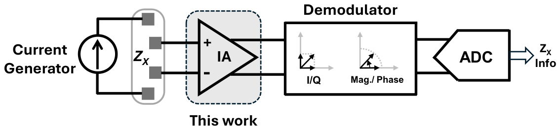
Figure 2.
Block diagram of polar demodulator architecture.
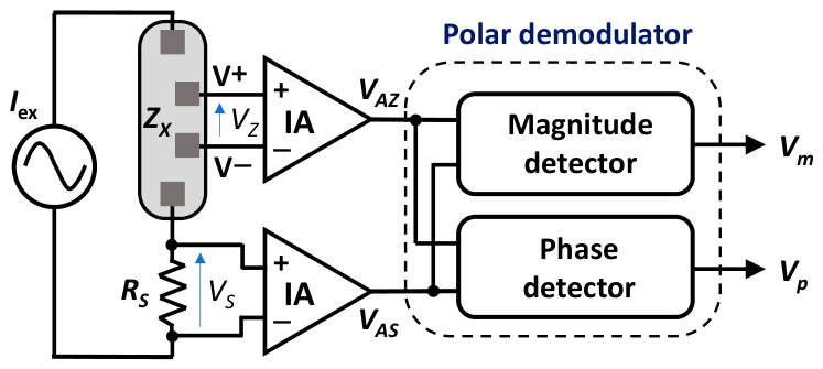
Figure 3.
Conceptual representation of the local current-feedback instrumentation-amplifier topology.
Figure 3.
Conceptual representation of the local current-feedback instrumentation-amplifier topology.
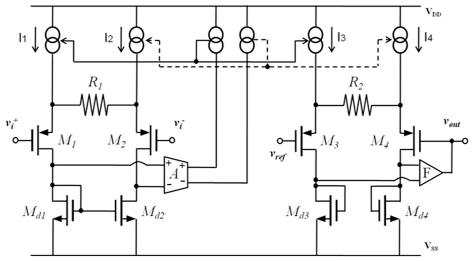
Figure 4.
Transistor-level implementation of the proposed CMOS CFIA: a) input stage and b) output stage.
Figure 4.
Transistor-level implementation of the proposed CMOS CFIA: a) input stage and b) output stage.
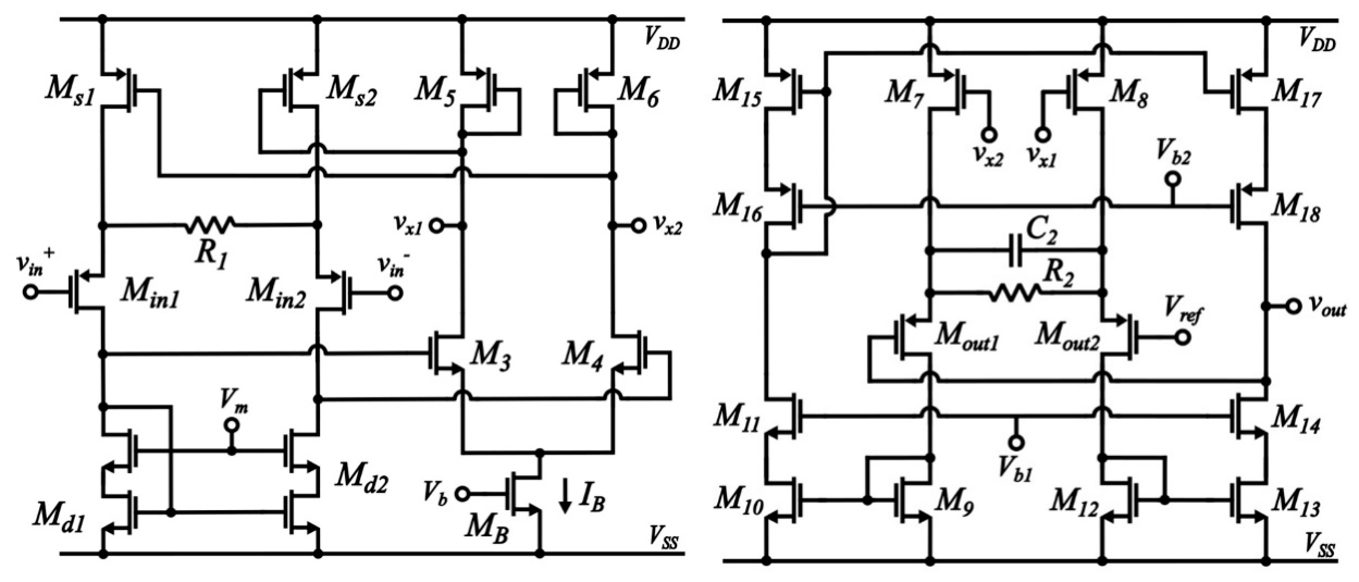

Table 1.
Specifications of CFIA.
| Specification | Requirement | Design relevance | Optimization |
| CMOS technology | 180 nm | Device models | Fixed |
| Supply voltage | 1.8 V | headroom/power | Constraint |
| Closed-loop gain | 30 V/V | signal amplification | Constraint |
| Signal-freq. range | 1 kHz – 1 MHz | BIS operating range | Constraint |
| Closed-loop BW | ≥ 2MHz | design margen | Constraint/objective |
Disclaimer/Publisher’s Note: The statements, opinions and data contained in all publications are solely those of the individual author(s) and contributor(s) and not of MDPI and/or the editor(s). MDPI and/or the editor(s) disclaim responsibility for any injury to people or property resulting from any ideas, methods, instructions or products referred to in the content. |
© 2026 by the authors. Licensee MDPI, Basel, Switzerland. This article is an open access article distributed under the terms and conditions of the Creative Commons Attribution (CC BY) license (http://creativecommons.org/licenses/by/4.0/).
Copyright: This open access article is published under a Creative Commons CC BY 4.0 license, which permit the free download, distribution, and reuse, provided that the author and preprint are cited in any reuse.