

Submitted:
25 September 2026
Posted:
28 September 2026
You are already at the latest version
Abstract
Through-silicon-carbide vias (TSiCVs) is a key technology for three-dimensional (3D) integration of silicon carbide (SiC) integrated circuits intended for extreme-environment applications such as Venus surface exploration. This work presents an expanded full-wave electromagnetic analysis using a Signal-Ground-Signal (SGS) configuration to evaluate the shielding effectiveness and signal integrity required for high-density 3D SiC packaging based on our previous study of Signal-Ground (SG) pairs. Parametric evaluation of Through-Silicon-Carbide Vias (TSiCVs) in a Signal-Ground-Signal (SGS) differential configuration operating across temperatures from 20°C to 600°C and with a frequency range of 1 GHz to 50 GHz and a systematic sweep of via radius (R=5 µm to 25 µm) is performed. Two distinct geometric scaling methodologies are evaluated for via radii with fixed pitch (P=52 µm) and proportional pitch scaling(P/D=2). Results demonstrate that physical geometry—specifically edge-to-edge spacing (S) dictates capacitive coupling and characteristic impedance matching (ZD11), whereas elevated temperature primarily drives ohmic attenuation (SD21) through enhanced conductor resistivity and skin-depth limitations. For the simulated 52 µm-pitch SGS channel, a via radius of R=10 µm provides the optimal wideband signal-integrity performance, achieving an optimal differential return loss (SD11) of -32.35 dB at 20°C and -39.09 dB at 600°C, and minimal insertion loss (SD21) of -0.045 dB at 50 GHz. Common-to-differential mode conversion (SCD21) remains suppressed below -64 dB across all temperature and geometric variations. These insights establish critical physical design trade-offs for high-density, extreme-environment 3D integrated circuits.
Keywords:
high-temperature electronics
; impedance
; Near-End crosstalk (NEXT)
; parasitic capacitance
; S-parameter analysis
; Through-Silicon-Carbide vias (TSiCV)
I. Introduction
The demand for high-performance electronics capable of operating in extreme environments has grown significantly, driven by space exploration missions to planetary surfaces like Venus, where ambient temperatures reach 460°C and pressures exceed 90 bar [1]. Silicon Carbide is a wide bandgap and high thermal conductivity material, which is why it is chosen for space exploration missions such as Venus surface [2,3]. Although significant advances have been made in SiC chips, reliable high-temperature interconnect packaging remains critical bottleneck [4,5]. Previous studies of high-temperature 3D SiC assemblies have examined wirebonded stacks [6], metal-to-metal flip-chip joints [7], SiC-on-alumina flip-chip assemblies [8], gold stud bumps for operation up to 600°C [9], and screen-printed alumina substrates [10]. Conventional 2D packaging, utilizing wire bonding or planar interconnects, introduces significant drawbacks: increased parasitic effects, restricted interconnect density, and compromised reliability in high-heat environments [11,12]. Vertical interconnects in three-dimensional (3D) architectures offer a viable strategy for optimizing interconnect density and reducing signal path lengths, while simultaneously facilitating heterogeneous integration [13,14]. Related 3D integration literature addresses micro-bump processing [15], die-to-wafer flip-chip bonding [16], and scaling optical on-chip interconnects [17]; medical applications illustrate another use of 3D packaging [18]. While TSVs are a proven concept, adapting them for SiC substrates introduces new complexities in material compatibility, fabrication constraints, and long-term thermal stability. Silicon carbide (SiC) outperforms silicon in terms of dielectric loss and heat dissipation; however, it introduces unique fabrication constraints, particularly regarding the etching and filling of high-aspect-ratio vertical interconnects [19,20]. Extreme-temperature TSiCV requires materials that can withstand 500 °C without degrading. Copper is often unsuitable due to oxidation and diffusion at these levels [21,22], whereas gold—despite its higher resistivity—provides the chemical stability and oxidation resistance necessary for Venus-class operating conditions [23]. The electrical performance of TSiCVs depends heavily on via geometry in addition to material selection. By influencing fundamental parasitic elements like inductance and capacitance, the via radius plays a critical role in shaping the overall signal integrity and power-delivery characteristics of the system [24]. More broadly, high-density system-on-package integration poses coupled signal- and power-integrity challenges [25].
Our previous work, which we shared in IEEE WMED-2026, focused on the basic electrical characteristics of gold-filled TSiCV using a simple Signal-Ground (SG) pair [26]. In this study, we transition from the basic SG pair analyzed in our previous work to a more robust Signal-Ground-Signal (SGS) architecture. While our preliminary study confirmed that gold-filled TSiCVs materials are feasible, the simple SG pairs used there don't provide the shielding needed for high-frequency SiC ICs. This paper expands that research by adopting a Signal-Ground-Signal (SGS) configuration—a much more accurate model for a shielded vertical line and under two design regimes: absolute layout density constraints (P=52 µm) and proportional pitch scaling(P/D=2).
II. Design Methodology
We adopt the Signal-Ground-Signal (SGS) configuration in this paper, as it provides a more robust analysis of electromagnetic isolation and Differential impedance than the Signal-Ground (SG) pair for achieving high-frequency signal integrity at 600° C in 3D integrated circuits (ICs).
A. Physical Geometry and Substrate Properties
The design of Through-Silicon-Carbide Vias (TSiCVs) is modeled in a SiC substrate box with a relative permittivity of 9.66 and a dielectric loss tangent of 0.001. The via depth is fixed at 100 µm, and to quantify the impact of parasitic coupling and cross-sectional area, the via radius () is swept through five discrete values: 5 µm, 10 µm, 15 µm, 20 µm, and 25 µm. The center-to-center pitch () between adjacent via structures is fixed at 52 µm. The physical edge-to-edge spacing () between adjacent via sidewalls is defined as:
where P is the pitch and R is the via radius. Pitch scales dynamically with via diameter (P=2D=4R), maintaining P/D=2 across R=5 µm to 25 µm (P=20 µm to 100 µm) and expanding edge-to-edge spacing as S=2R. Figure 1a shows a 3D view of the materials used in our geometry, and Figure 1b shows the side view with the signal TSiCV on the left, the right, and the ground TSiCV in the center between two signal vias. The entire SiC substrate was enclosed in an air-filled radiation boundary to accurately simulate an open environment. The current simulation model assumes a smooth conductor-to-dielectric interface to establish a baseline for the electrical and thermal trade-offs of the TSiCV geometry, while the full-wave electromagnetic solver inherently accounts for proximity effects within the signal-ground pair configuration.
B.Material Stack and Insulation
To prevent metal diffusion into the SiC substrate at extreme temperatures, a comprehensive material stack is implemented. Liner of 0.5 µm as shown in Table I thick silicon dioxide (SiO2) layer provides electrical isolation between the gold core and the semi-insulating substrate. A barrier of 0.1 µm thick, as shown in Table I, Tantalum Nitride (TaN) layer is placed between the liner and the conductive core to act as a diffusion barrier and adhesion promoter. Gold is used as a filler material as a conductive core.
C. Thermal Modelling
Thermal modeling is designed in Ansys HFSS by modifying material properties such as thermal modifiers, and a temperature variable is defined and assigned in Opti Metrics as a parametric setup. To accurately model the conductor losses, the gold core’s resistivity was linked to the temperature variable using the standard linear temperature coefficient of resistance (TCR) formula [27]:
where ρ0 is the resistivity of the gold at reference temperature (20°C), α is the temperature coefficient of resistance given in Table I, T0 is the reference temperature, and T is the actual temperature of the material during operation. Since HFSS uses conductivity, we inverted the formula and entered it into the edit libraries.
The substrate is modeled as semi-insulating Silicon Carbide () with baseline room-temperature(T0=20°C) dielectric properties defined as ϵr,0=9.7 and a nominal loss tangent . To account for thermal excitation and dielectric dissipation up to continuous mathematical functions of temperature () were assigned to the material definition:
Relative Permittivity: Evaluated using a first-order linear thermal coefficient model:
where represents the linear temperature coefficient of permittivity.
Dielectric Loss Tangent: Formulated using an exponential thermal scaling function to capture the rapid increase in substrate dielectric absorption at elevated temperatures:
where is the exponential thermal coefficient governing dielectric loss scaling.
To maintain consistency across dielectric interfaces, the silicon dioxide () insulating layer is governed by analogous linear thermal relations.
D. Extraction of Electrical Parameters
The lumped equivalent circuit parameters are extracted from the simulated S-parameters and Y-parameters.
III. Simulation Results
Full-Wave Electromagnetic simulations are performed using ANSYS HFSS from 1 GHz to 50 GHz. The frequency-dependent skin effect is accounted for by using high density mesh at the via interfaces. The signal integrity of the gold-filled TSiCV structure was evaluated using a mixed-mode S-parameter analysis to distinguish between differential and common-mode performance.
A. Differential Impedance Analysis
We have extracted Differential Impedance (ZD11) to evaluate the impedance matching for the vertical interconnect under high-speed differential signaling.
Geometric Impact: At lower frequencies(1GHz), as shown in Figure 2. ZD11 is predominantly inductive and capacitive. As the via radius increases from 5µm to 25 µm, ZD11 decreases monotonically from 84.65Ω to 64.67Ω at 20°C, as shown in Table II and Figure 2. This drop is driven by the severe reduction in edge-to-edge spacing (S decreasing from 42 µm to 2 µm), which increases parasitic capacitance per unit length.
Frequency Dispersion: As frequency increases to 50GHz, parasitic capacitance and proximity effects compress the impedance towards 50Ω. Specifically, R=10 µm (S=32 µm) yields ZD11 = 47.58Ω at 20°C, offering an exceptional match to 50Ω system lines.
Thermal Stability: Thermal elevation to 600° C induces minimal shift in ZD11 (<0.7Ω variation across all radii). This confirms that high-frequency differential impedance is governed almost entirely by structural dimensions rather than thermal variations in metal resistivity.
B. Capacitance Analysis
Parasitic capacitance determines the RC delay and the ultimate bandwidth limit of the vertical interconnect. In the SGS configuration, parasitic capacitance is evaluated as two components: mutual signal-to-signal coupling capacitance (Cm) and self-signal-to-ground capacitance (Cself). As detailed in Table III mutual capacitance (Cm) increases monotonically from 14.97(fF) to 18.20(fF) at 20°C due to expanding sidewall area of adjacent signal vias. Simultaneously, self-capacitance (Cself) experiences much steeper increase rising from 80.86(fF) to 662.19(fF) at 20°C. This extreme capacitive loading occurs because the signal-to-ground sidewall gap contracts to just 2 µm at R=25 µm, creating a dominant parallel-plate capacitance across the 0.5 µm SiO2 isolation liner.
As shown in Figure 3a and Figure 3b, temperature elevation results in a slight, consistent reduction in both mutual capacitance (Cm) and Self-Capacitance (Cself) across all evaluated via radii. Specifically, elevating the temperature from 20°C to 600°C induces a minimal reduction in mutual capacitance—dropping by less than 0.55% in the fixed-pitch regime (P=52 µm).
C. Near-End-Crosstalk (NEXT)
By adopting the SGS configuration, we have achieved isolation between the signal paths. We found that the size directly correlates with electromagnetic coupling. Increasing the via radius significantly suppresses crosstalk, as shown in Figure 4. Improves from -19.90 dB (R=5 µm) to -26.92 dB (R=25 µm) at 20°C, as shown in Table IV. Larger central ground vias present a greater cross-sectional area, terminating electric field lines more effectively and preventing field leakage between the two signal vias. Temperature changes between 20° C and 600°C alter by less than 0.5dB. This proves that crosstalk suppression in SGS TSiCV arrays is structurally determined by spatial geometry rather than temperature-dependent conductor losses.
D. Mixed-Mode S-Parameter Analysis and Transmission Efficiency
To evaluate broadband differential signal transmission, reflection, and mode transformation within the SGS TSiCV array, full-wave mixed-mode S-parameters were extracted from 1GHz to 50GHz across temperatures from 20°C to 600°C. The complete dataset, including differential return loss (SD11), differential insertion loss (SD21), common-mode insertion loss (SC21), and common-to-differential mode conversion (SCD21), is summarized in Table V
Increasing temperature consistently degrades insertion loss due to metal resistivity, and signal attenuation is also increases with increasing radius.
(C) Mode conversion and Common Mode Rejection:
SCD21 remains strongly suppressed (<- 63.9 dB) across all frequencies, radii, and thermal conditions. This suppression confirms the high geometric symmetry of the SGS architecture and the dielectric uniformity of the SiC substrate.
Design Implication: For the optimal R=10 µm configuration, SCD21remains below -77.06 dB up to even at 600°C a shown in Figure 5c. This demonstrates that the proposed TSiCV structure effectively prevents common-mode environmental noise from compromising signal integrity in high-temperature 3D SiC ICs.
E. Design Tradeoffs
While the R= 10 µm geometry represents the optimal single-design point for wideband 50 Ω differential channels (SD11<-32dB, SD21=-0.045dB), practical 3D System-on-Chip (SoC) architectures demand distinct geometric optimizations based on signal type. For ultra-high-speed digital clock and data lines where parasitic capacitance dictates the upper bandwidth boundary, smaller vias (R=5 µm) offer a reduced parasitic capacitance of 14.92fF at 600°C.
Conversely, for power delivery networks (PDN) and low-frequency analog interconnects, larger via radii (R=25 µm) provide superior DC/AC -drop mitigation and enhanced ground shielding, achieving a crosstalk isolation of at . Therefore, an application-specific dual-geometry (mixed-via) approach deploying 5 µm to 10 µm for high-frequency signal channels and 25 µm vias for power and shielding trunks—enabling simultaneous optimization of signal integrity and thermal/electrical power delivery in extreme-environment 3D ICs.
(2)
- Capacitance is extracted from the imaginary part of admittance.
- Differential Impedance is extracted from the Z-parameters to evaluate the impedance matching the vertical interconnect.
- Near-end crosstalk (NEXT) is extracted as the coupling coefficient between the adjacent signal and ground vias in the SGS configuration.
- (a)
- Differential Return Loss(SD11 ): As shown in Figure 5a and Table V, differential return loss(SD11) is less effected with temperaure, but it is more impact with radius. Increasing the radius beyond 15 µm significantly degrades the impedance matching. At R=25 µm(50GHz), SD11 deteriorates to -6.26 dB(20° C) and -5.97 dB(600° C) as shown in Figure 5a due to parasatic capacitance dominance.
- (b)
- Diffrential Insertion Loss(SD21): At low frequncies, insertion loss remains minimal(<0.1 dB) for R≤20 µm as shown in Figure 5b. At 50 GHz, signal attenuation increases considerably with larger dimensions. The optimal performance is observed at R=10 µm with a low insertion loss of -0.045 dB to -0.072 dB, maintaining acceptable operational performance.
IV. Proportional Pitch Scaling Study
To isolate the effects of normalized geometric scaling from fixed layout boundaries, a parallel parametric sweep was conducted where pitch scaled proportionally with diameter(P=2D=4R) for R=5 µm to 25 µm.
A. Differential Impedance (ZD11) and Parasitic Capacitance
Maintaining P/D=2 normalizes the electric field geometry and yields consistent characteristic impedance. As shown in Table VII and Figure 6a, at 1 GHz, ZD11 remains invariant across all via radii. At 50 GHz, high frequency dispersion holds ZD11 within 46.17Ω to 46.95Ω.As presented in Table VI, both mutual coupling capacitance (Cm) and self-Capacitance (Cself) exhibit a monotonic decrease as the via radius increases.
Mutual Capacitance: At 20°C, Mutual capacitance decreases from 33.54(fF) to 7.08(fF) at R=25 µm. This represents an overall reduction of 78.9%, demonstrating that increasing physical signal-to-signal separation effectively suppresses mutual capacitive coupling despite the larger sidewall surface area.
Self-Capacitance: Self-capacitance similarly decreases from 170.79(fF) to 127.51(fF) at 20°C. Expanding the signal-to-ground gap increases the effective dielectric path length between conductors, which outweighs the surface area expansion of the via sidewall.
As illustrated in Figure 6a and Figure 6b, temperature elevation from 20°C to 600°C results in a slight, consistent reduction in both mutual capacitance and self-capacitance across all radii. Across the entire temperature range, Mutual Capacitance decreases by only 0.54% to 0.85%, while self-capacitance drops by 0.94% to 2.56%. This minor variation confirms the exceptional thermal stability of the isolation liner, proving that parasitic capacitance in the proportional scaling regime is governed almost entirely by physical geometry rather than thermal stress.
B. Near-End Crosstalk
Near-end crosstalk in the array remains well-suppressed due to central ground via isolation. As detailed in Table VIII and Figure 7, NEXT improves from () to (). Temperature variation between 20 °C and 600 °C alters NEXT by less than , reconfirming that crosstalk isolation is dictated by spatial geometry rather than thermal variation in metal resistivity.
C. Mixed Mode S Parameters.
Mixed-mode S-parameters were extracted from 1 GHz to 50 GHz across temperatures.
Differential Return Loss (): scaling preserves wideband impedance matching. At 50 GHz, reaches for and improves continuously (as shown in Figure 8a to for at 20 °C ( at 600 °C as shown in Table IX).
Differential Insertion Loss (): Signal attenuation remains low. At 50 GHz, ranges between () and () at 20 °C. At 600 °C, attenuation increases slightly due to elevated gold resistivity, keeping between and Mode Conversion (): Common-to-differential mode conversion remains suppressed below across all conditions, confirming structural symmetry.
V. Comparative Analysis
Comparing fixed pitch () against proportional scaling () highlights critical trade-offs for high-temperature 3D interposer design.
Impedance Stability vs. Density Constraints: Fixed pitch layout constraints force to drop by over ( at 1 GHz) as via radius increases. Conversely, proportional scaling () maintains stable impedance ( at 1 GHz; at 50 GHz) across all radii, providing predictable differential matching.
Capacitance Dynamics: In fixed pitch arrays, parasitic capacitance increases with radius () due to narrowing gap spacing . Under scaling, capacitance decreases sharply () because expanding pitch widens absolute spacing High-Frequency Attenuation (, 50 GHz, 600 °C): Fixed pitch channels suffer severe reflection () and insertion loss () at large radii. Proportional scaling maintains excellent matching () and minimal loss ().
VI. Conclusion
This paper has presented a comprehensive investigation into the design and electrical performance of gold-filled Through-Silicon-Carbide Vias (TSiCV) in a Signal-Ground-Signal (SGS) configuration, specifically optimized for the 600°C extreme environment of Venus. By transitioning from a basic Signal-Ground pair to a shielded SGS architecture, we have quantified the critical trade-offs between vertical interconnect density and electromagnetic signal integrity up to 50 GHz. The simulation results lead to several key conclusions for the development of high-temperature 3D SiC integrated systems.
This work establishes a comprehensive physical framework for TSiCV signal integrity in high-temperature 3D integrated systems. The analysis decoupling physical mechanisms confirms that via geometry (R, S) dictates capacitive loading and differential impedance matching, whereas operational temperature (20°C to 600°C) primarily controls conductor skin loss and attenuation. For a fixed 52 µm-pitch SGS channel, a via radius of R=10 µm (S=32 µm) represents the optimal trade-off point, yielding a near-ideal 50Ω match (47.58Ω), minimum reflection (S11 <- 32 dB), low insertion loss (Sd21=-0.045 dB), and strong mode conversion rejection (Scd21<-75dB) up to Proportional Scaling (): Best for impedance-critical high-speed differential signal channels.
Furthermore, we have identified a clear design path for future SiC SoCs: a dual-geometry approach. With our Mixed via strategy, engineers can optimize both the electrical efficiency and thermal reliability of next-generation high-temperature electronics.
VII. FutureWork
Future work will extend this analysis to include reliability of physics, such as electromigration and stress migration. Beyond the foundational SGS configuration, we intend to investigate dense "via farms" by varying pitch distances.
Finally, we plan to conduct experimental characterization of fabricated TSiCV samples to empirically validate the high-temperature performance reported in this simulation study.
Funding
This work was supported in part by the National Aeronautics and Space Administration (NASA) under Grant 80NSSC25M0049 and in part by the Micron Foundation. (Corresponding author: Feng Li). Recommended for publication by Associate Editor upon evaluation of reviewers’ comments.
References
- Casady, J.; Johnson, R. W. Status of silicon carbide (SiC) as a wide bandgap semiconductor for high-temperature applications: A review. Solid-State Electron. 1996, vol. 39(no. 10), 1409–1422. [Google Scholar] [CrossRef]
- Van Cuong, V.; Meguro, T.; Ishikawa, S.; Maeda, T.; Sezaki, H.; Kuroki, S.-I. Amplifier based on 4H-SiC MOSFET operation at 500◦C for harsh environment applications. IEEE Trans. Electron Devices 2022, vol. 69(no. 8), 4194–4199. [Google Scholar] [CrossRef]
- Mo, J.; Middelburg, L. M.; Morana, B.; van Zeijl, H. W.; Vollebregt, S.; Zhang, G. Surface-micromachined silicon carbide Pirani gauges for harsh environments. IEEE Sens. J. 2020, vol. 21(no. 2), 1558–1748. [Google Scholar]
- Seal, S.; Mantooth, H. A. High performance silicon carbide power packaging—Past trends, present practices, and future directions. Energies 2017, vol. 10(no. 3), 341. [Google Scholar] [CrossRef]
- Neudeck, P. G.; Spry, D. J.; Krasowski, M. J.; Chang, C. W.; Gonzalez, J. M.; Rajgopal, S.; Prokop, N. F.; Greer, L. C.; Lukco, D.; Maldonaldo-Rivera, S.; Adams, C. M. Recent progress in extreme environment durable SiC JFET-R integrated circuit technology. In IMAPSource Proc.; Power, Oct 2023; vol. 2023, no. HiTEC, CICMT. [Google Scholar] [CrossRef]
- Li, F.; Raveendran, S. Wirebonding based 3D SiC IC stacks for high temperature applications. Proc. IEEE 72nd Electron. Compon. Technol. Conf. (ECTC), 2022; pp. 2023–2027. [Google Scholar] [CrossRef]
- Li, F.; Shi, J. Metal-to-metal flip-chip bonding for high-temperature 3D SiC IC integration and packaging. Proc. IEEE Workshop Microelectron. Electron Devices (WMED), Boise, ID, USA, 2023. [Google Scholar] [CrossRef]
- Li, F.; Lamsal, B.; Shi, J. Flip-chip bonding of SiC chips onto alumina substrate for high temperature applications. Proc. IEEE Workshop Microelectron. Electron Devices (WMED), Boise, ID, USA, 2024; pp. 1–4. [Google Scholar] [CrossRef]
- Li, F. Flip chip bonding for SiC integrated circuits with gold stud bumps for high temperature up to 600C applications. IEEE Trans. Compon. Packag. Manuf. Technol. 2024, vol. 14(no. 4), 705–713. [Google Scholar] [CrossRef]
- Li, F.; Shi, J.; Lamsal, B. Flip chip bonding of SiC chips on screen printed alumina substrate for high temperature applications. IEEE Trans. Compon. Packag. Manuf. Technol. 2025, vol. 15(no. 6), 1359–1366. [Google Scholar] [CrossRef]
- Li, J.; Liu, L.; Deng, L.; Ma, B.; Wang, F.; Han, L. Interfacial microstructures and thermodynamics of thermosonic Cu-wire bonding. IEEE Electron Device Lett. 2011, vol. 32(no. 10), 1433–1435. [Google Scholar] [CrossRef]
- Chen, L.; Neudeck, P. G.; Spry, D. J.; Beheim, G. M.; Hunter, G. W. A 96% alumina-based packaging system for 500°C test of SiC integrated circuits. In IMAPSource Proc.; CICMT, Power, Apr 2021; vol. 2021, no. HiTEC, pp. 000069–000075. [Google Scholar] [CrossRef]
- Lau, J. H. Overview and outlook of through-silicon via (TSV) and 3D integrations. Microelectron. Int. 2011, vol. 28(no. 2), 8–22. [Google Scholar] [CrossRef]
- Li, Feng. 3D stacking of Sic integrated circuit chips based on gold wire-bonded interconnects for long-duration high-temperature applications. IEEE Trans. Compon. Packag. Manuf. Technol. 2022, vol. 12(no. 10), 1601–1608. [Google Scholar] [CrossRef]
- Li, F.; Li, Q.; Owens, A. Micro-bump processing for 3D IC integration. IMAPS Addit. Conf. (Device Packaging, HiTEC, HiTEN, and CICMT) 2019, vol. 2019, no. DPC, 001028–001049. [Google Scholar] [CrossRef]
- Di Cino, M.; Li, F. Flip chip die-to-wafer bonding review: Gaps to high volume manufacturing. Semicond. Sci. Inf. Devices 2022, vol. 4(no. 1), 8–13. [Google Scholar] [CrossRef]
- Binggeli, M.; Li, F. Scaling optical communication for on-chip interconnect. Proc. 19th Int. Conf. Electron. Packag. Technol. (ICEPT), 2018; pp. 1178–1183. [Google Scholar] [CrossRef]
- Yang, Y.; Li, F. Recent advances in 3D packaging for medical applications. Proc. 19th Int. Conf. Electron. Packag. Technol. (ICEPT), 2018; pp. 1193–1197. [Google Scholar] [CrossRef]
- Wang, X.; Chen, D.; Li, D.; Kou, C.; Yang, Y. The development and progress of multi-physics simulation design for TSV-based 3D integrated system. Symmetry 2023, vol. 15(no. 2), 418. [Google Scholar] [CrossRef]
- Elasser; Chow, T. P. Silicon carbide benefits and advantages for power electronics circuits and systems. Proc. IEEE 2002, vol. 90(no. 6), 969–986. [Google Scholar] [CrossRef]
- Zolper, J.C. Emerging silicon carbide power electronics components. In Proceedings of the Twentieth Annual IEEE Applied Power Electronics Conference and Exposition, Austin, TX, USA, 6–10 March 2005; Volume 1, pp. 11–17. [Google Scholar]
- Kirsch, P. D.; Ekerdt, J. G. Chemical and thermal reduction of thin films of copper (II) oxide and copper (I) oxide. J. Appl. Phys. 2001, vol. 90(no. 8), 4256–4264. [Google Scholar] [CrossRef]
- McBrayer, J. D.; Swanson, R. M.; Sigmon, T. W. Diffusion of metals in silicon dioxide. J. Electrochem. Soc. 1986, vol. 133(no. 6), 1242–1246. [Google Scholar] [CrossRef]
- Liu, P. S.; Wu, C. G.; Du, J. C. Study on transmission characteristics of TSV. J. Phys. Conf. Ser. 2018, vol. 986(no. 1), 012008. [Google Scholar] [CrossRef]
- Totorica, N.; Li, F. Signal and power integrity challenges for high density system-on-package. Semicond. Sci. Inf. Devices 2022, vol. 4(no. 2), 1–9. [Google Scholar] [CrossRef]
- Thota, S.; Song, L.; Li, F. Design Tradeoffs of Through-Silicon-Carbide Vias for High-Temperature 3D SiC IC Integration. 2026 IEEE Workshop on Microelectronics and Electron Devices (WMED), Boise, ID, USA, 2026; pp. 10–13. [Google Scholar] [CrossRef]
- Akter, A. Sharif; Mahbub, R. “Gold-based interconnect for high temperatures and harsh environments,” in Power Electronic Packaging: Design, Materials, Post-Fabrication and Reliability, 1st ed.; McCluskey, F. P., Yoon, S. W., Eds.; Wiley: Hoboken, NJ, USA, 2019; Volume Ch. 8, pp. 201–222. [Google Scholar]
Figure 1a.
3D electrical simulation model of S-G-S structure in TsiCV.
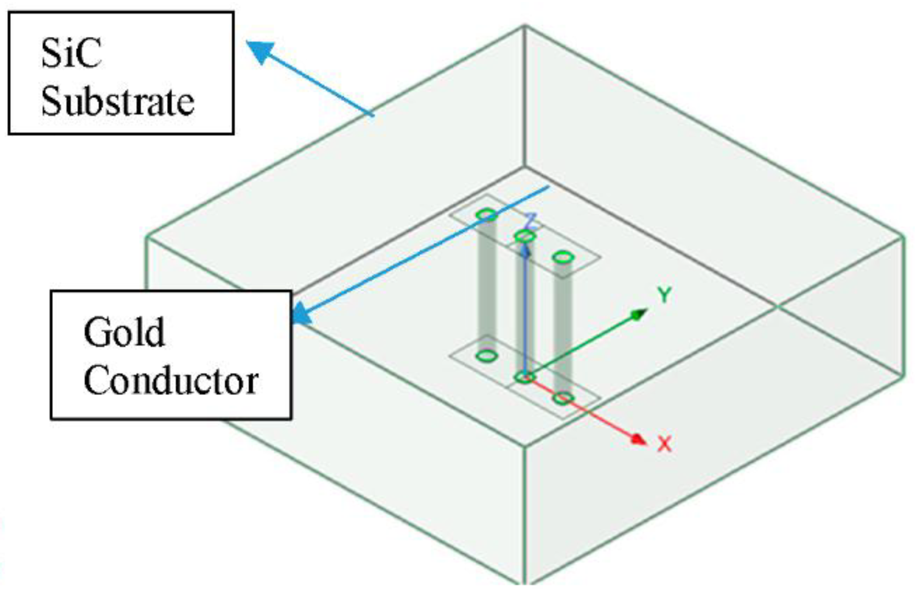
Figure 1b.
Cross-sectional view of S-G-S structure in TSiCV.
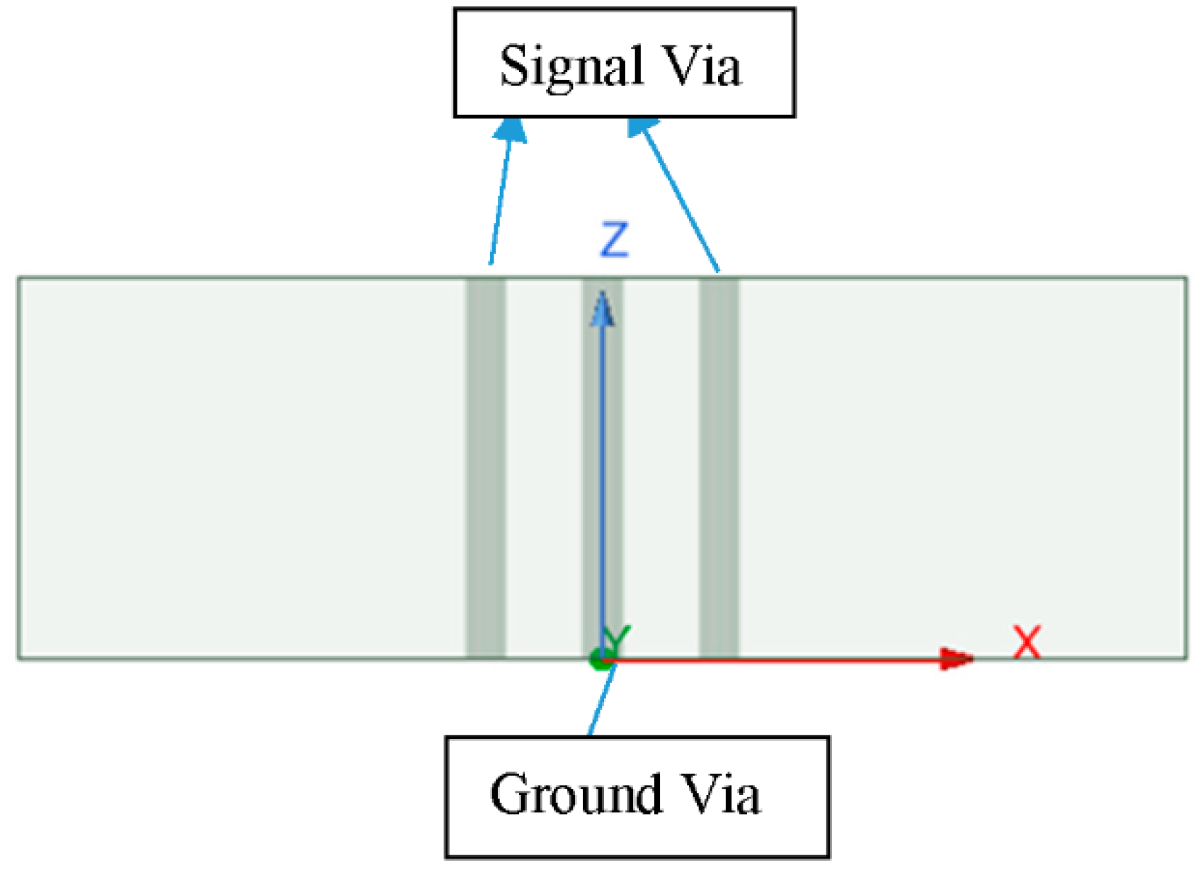
Figure 2.
Impedance with varying radius and temperature.
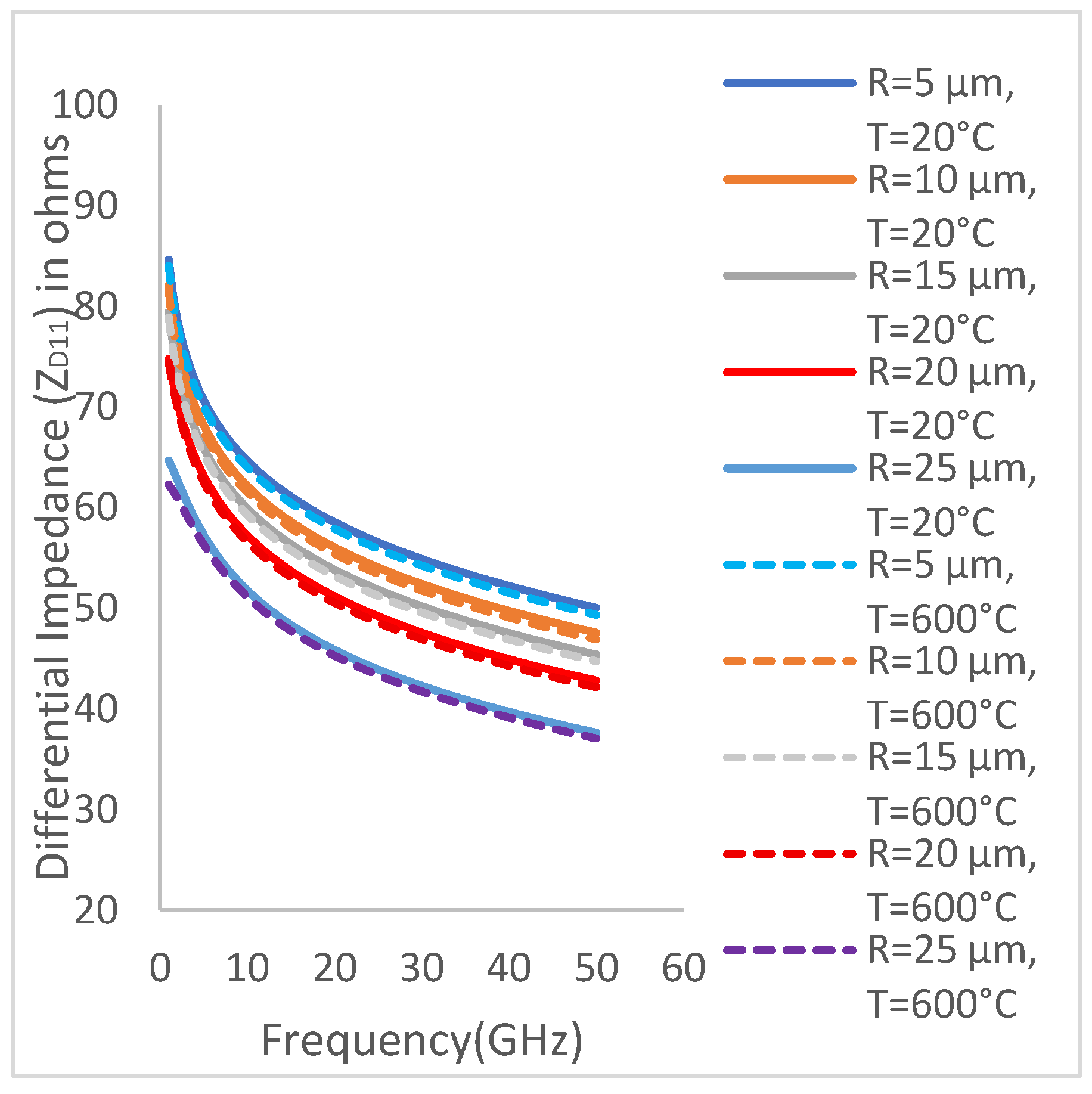
Figure 3a.
Mutual Capacitance with varying radius and temperature.
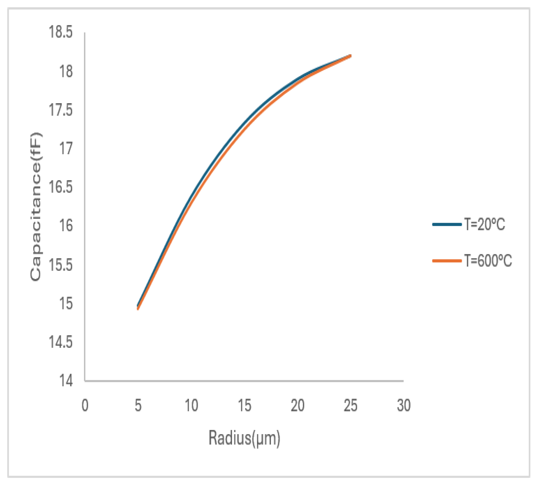
Figure 3b.
Self-Capacitance with varying radius and temperature.
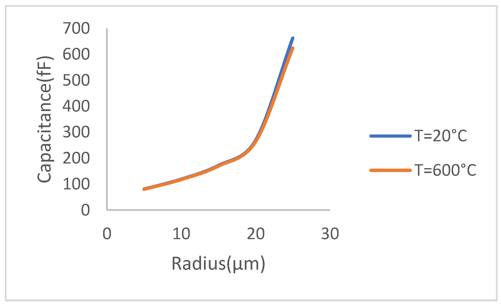
Figure 4.
NEXT values with varying radius and temperature.
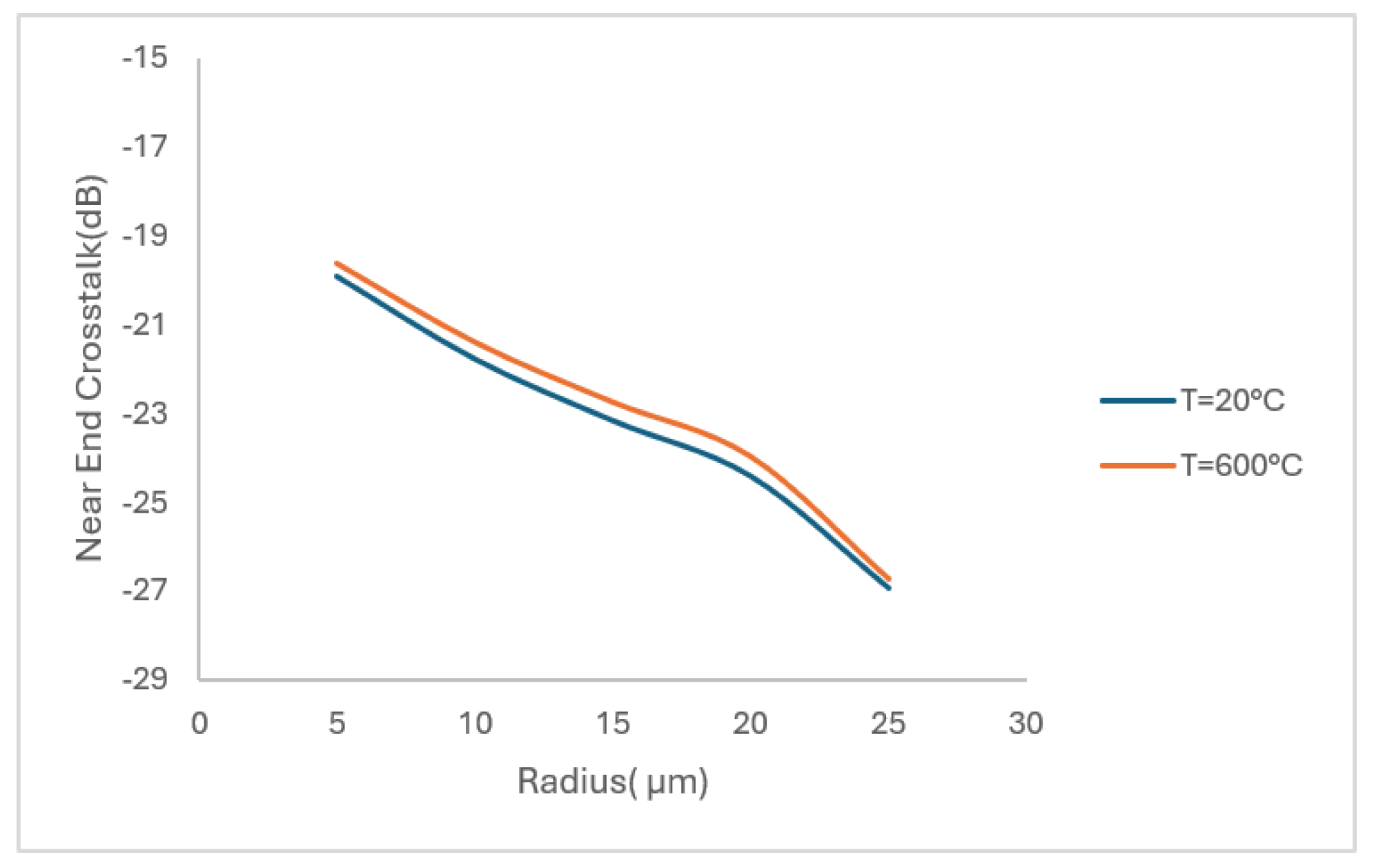
Figure 5a.
Differential Return Loss (Sd11) with varying radius and temperature.
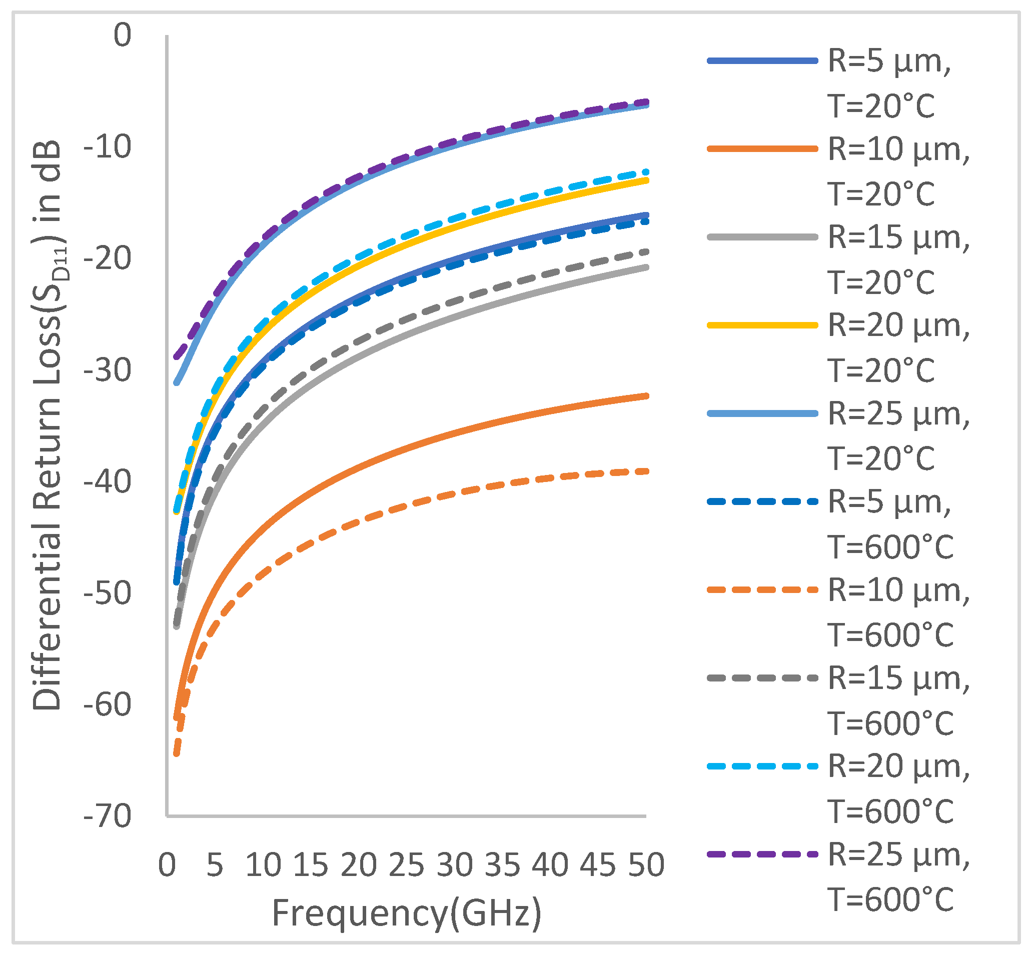
Figure 5b.
Differential Insertion loss (SD21) with varying radius and temperature.
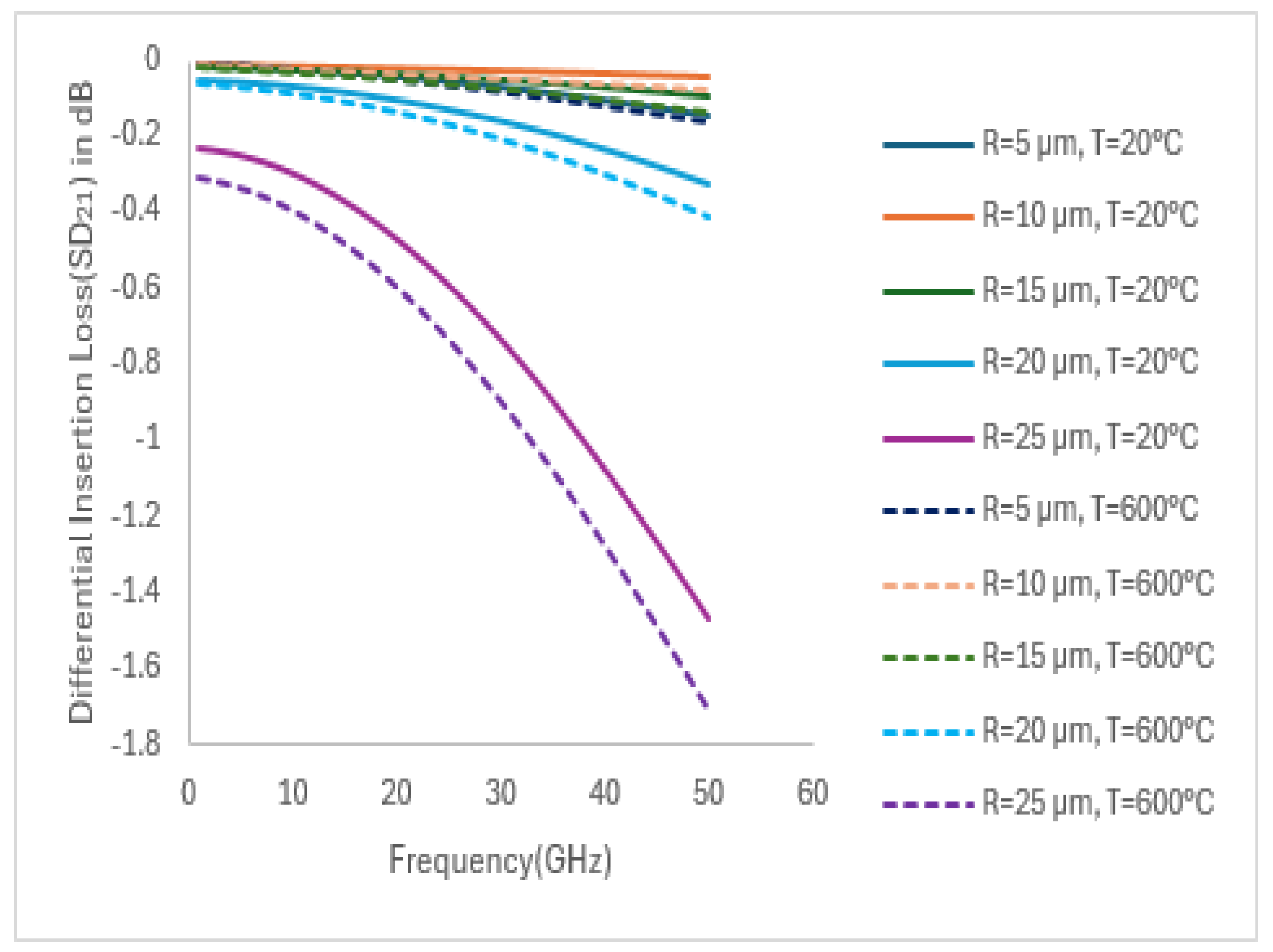
Figure 5c.
Common-to-differential mode conversion loss (SCD21) with varying radius and temperature.
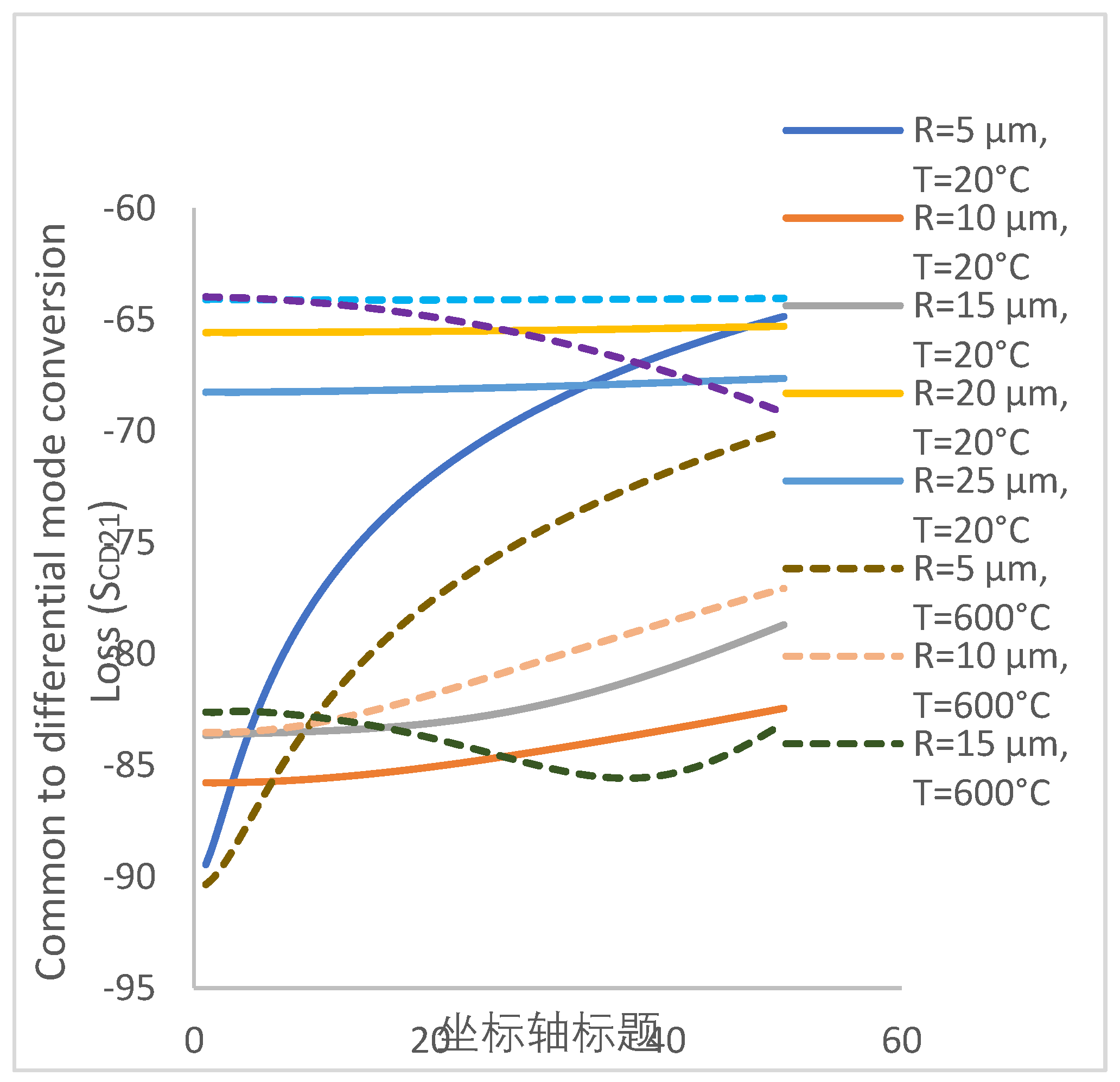
Figure 6a.
Differential Impedance (ZD11) for Pitch Scaling.
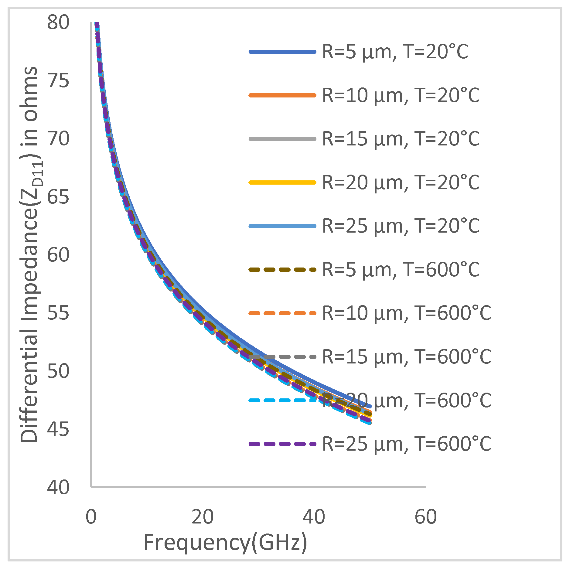
Figure 6b.
Mutual Capacitance for Pitch Scaling.
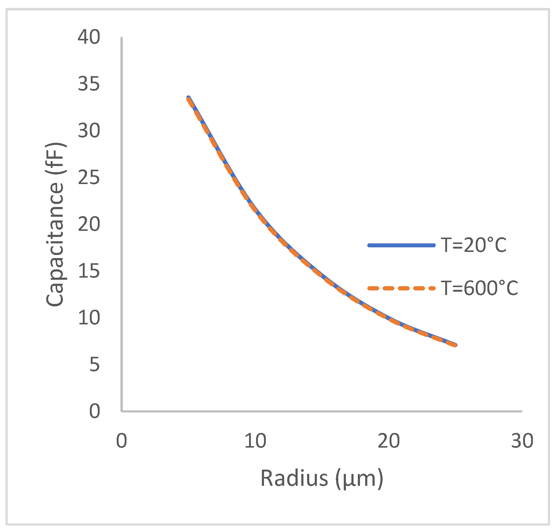
Figure 6c.
Self-Capacitance for Pitch Scaling.
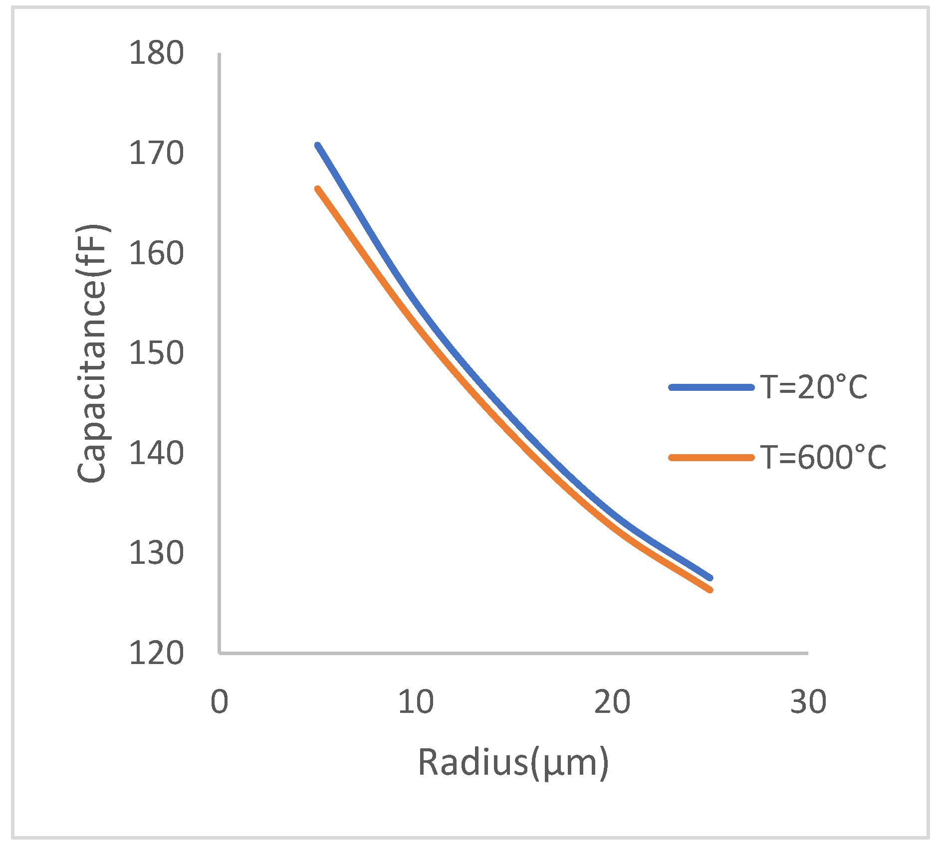
Figure 7.
Near-end crosstalk (pitch Scaling).
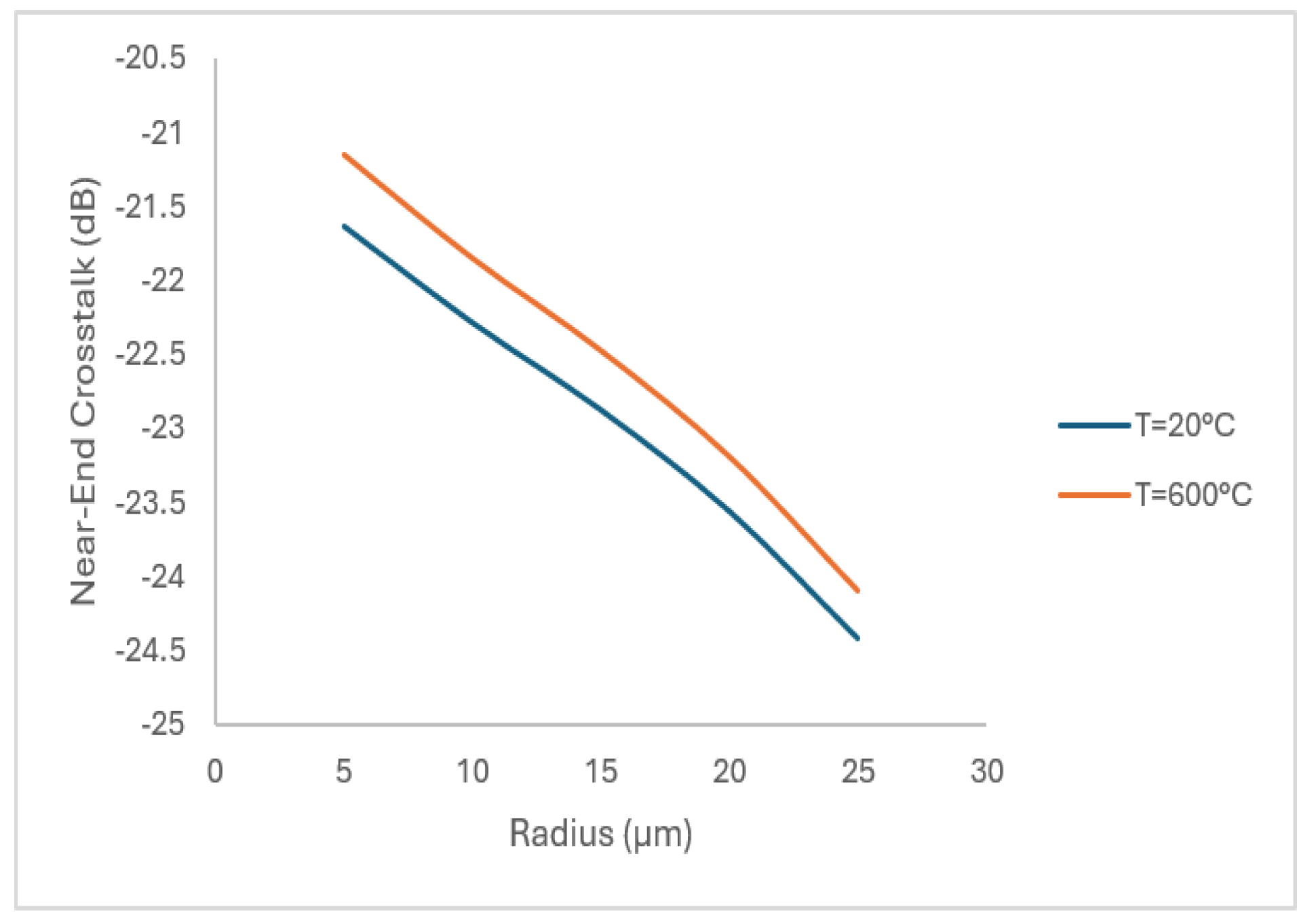
Figure 8a.
Differential Return Loss (SD11) for Pitch Scaling.
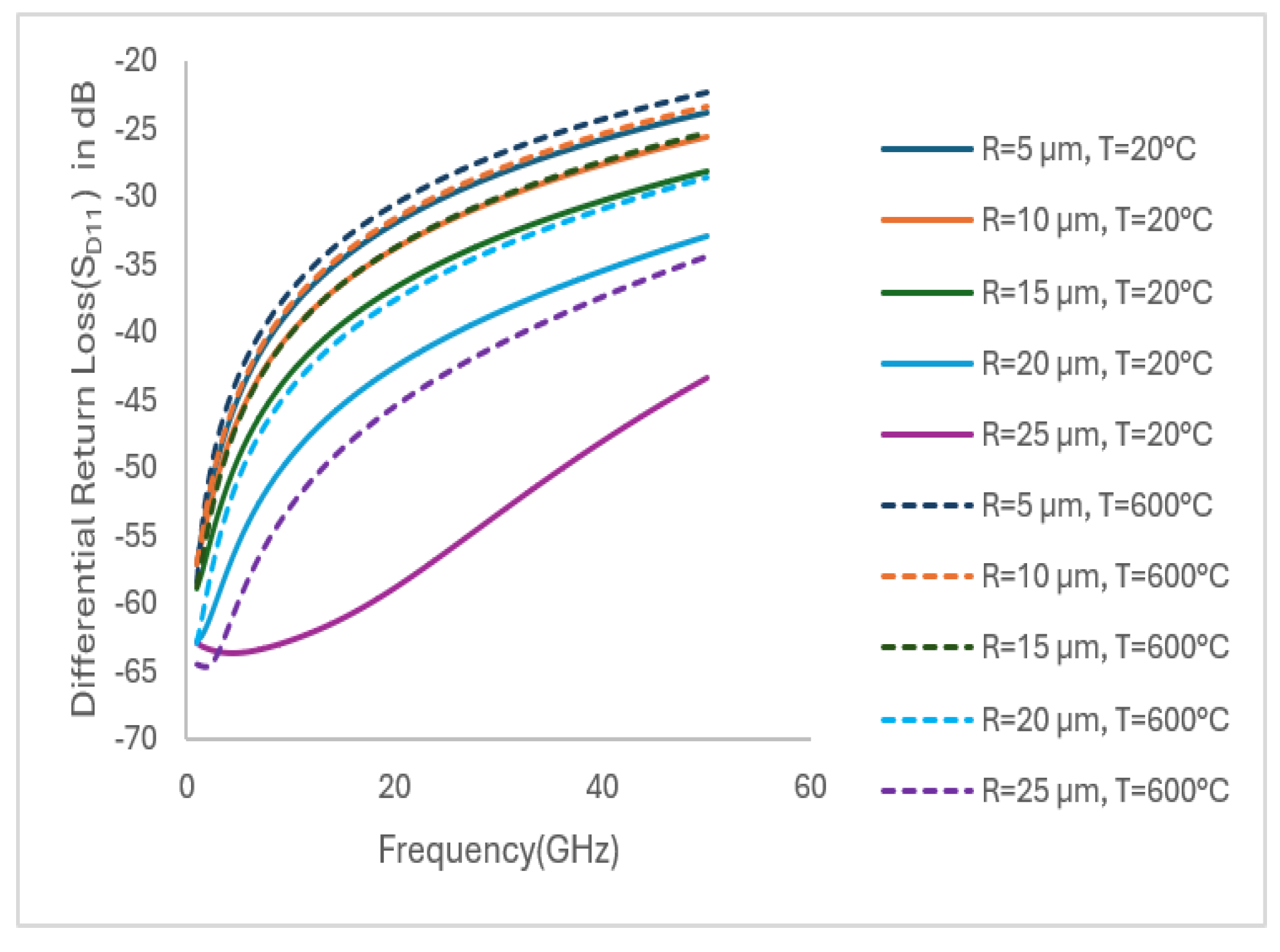
Figure 8b.
Differential Insertion Loss (SD21) for Pitch scaling.
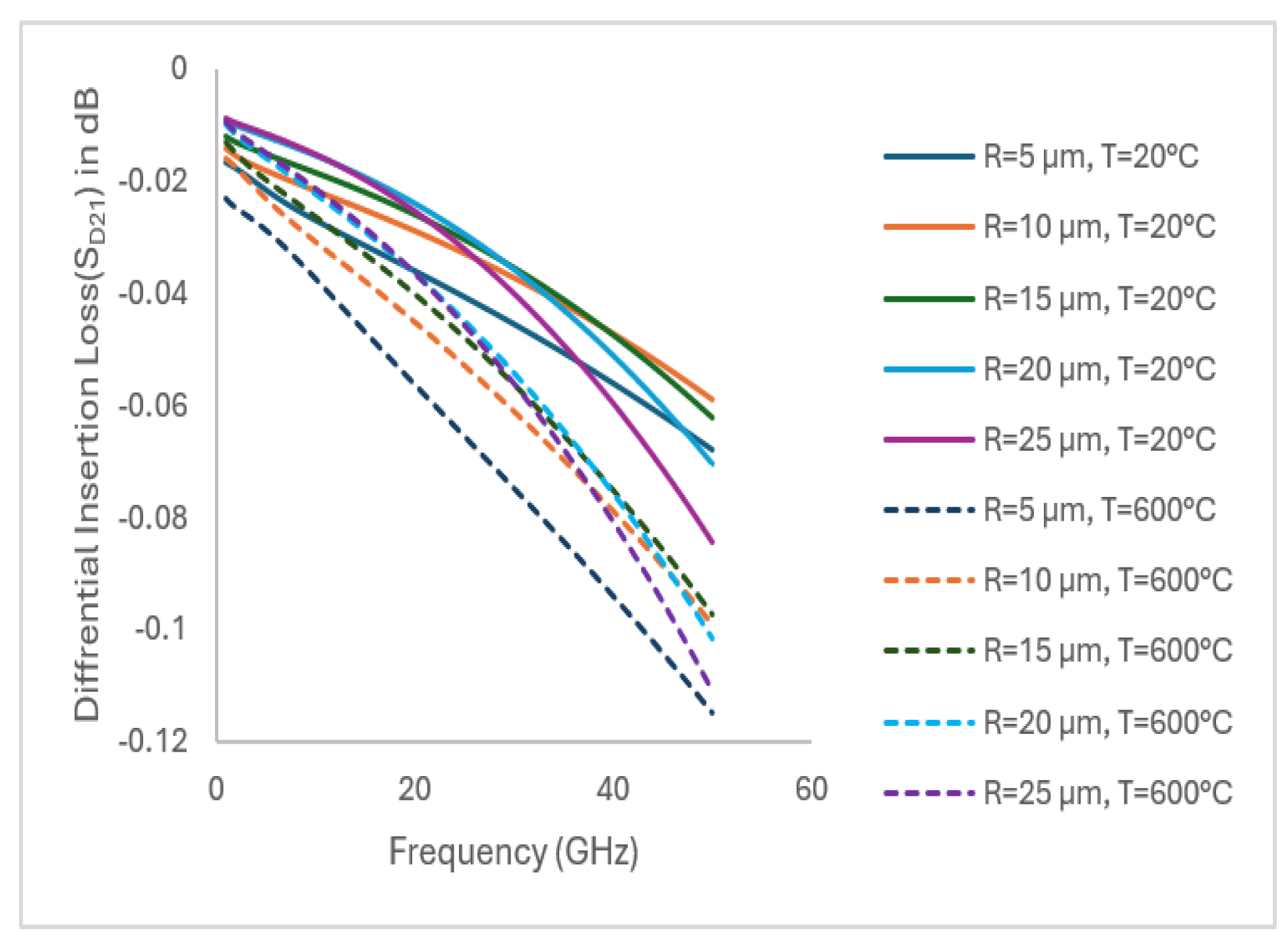
Figure 8c.
Mode Conversion (SCD21) for pitch scaling.
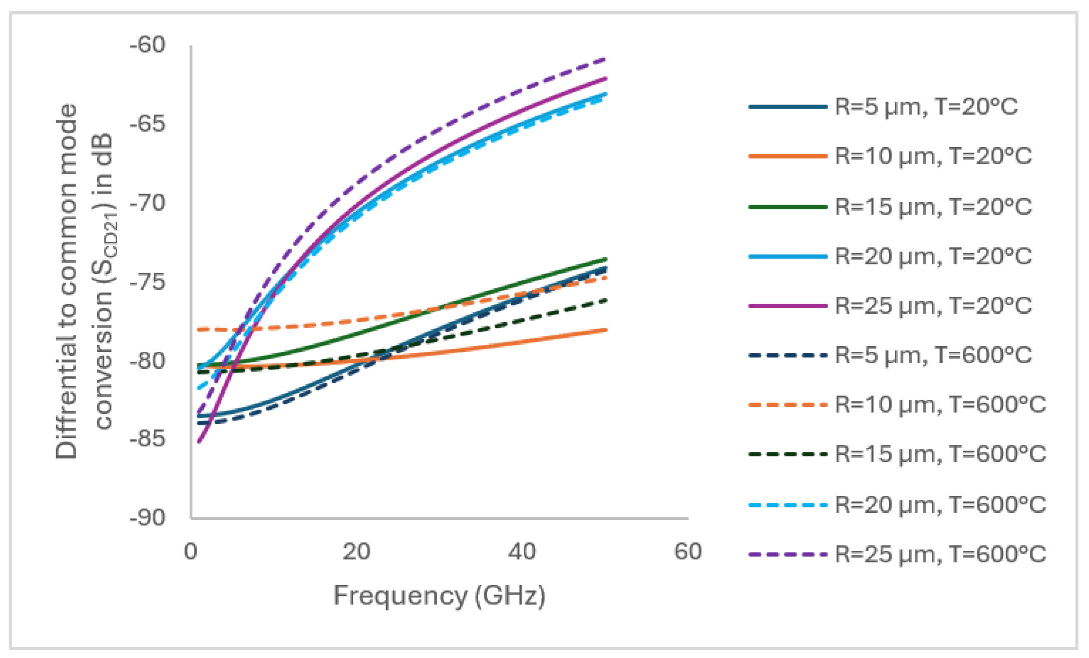

Table 1.
Parameters of the tsicv structures.
Table 2.
Differential impedance values.
| Differential Impedance(Ω) |
Frequency (GHz) | R=5 μmT=20°C | R=10 μm,T=20°C | R=15 μm,T=20°C | R=20 μm,T=20°C | R=25 μm T=20°C |
R=5 μm T=600°C | R=10 μm T=600°C | R=15 μm, T=600°C | R=20 μmT=600°C | R=25 μm T=600°C |
| ZD11 | 1 | 84.65 | 82.06 | 79.43 | 74.76 | 64.67 |
84.02 |
81.44 |
78.90 |
74.38 |
62.29 |
| ZD11 | 50 | 50.04 | 47.58 | 45.40 | 42.82 | 37.64 |
49.35 |
46.90 |
44.74 |
42.15 |
37.06 |
Table 3.
Capacitance values.
| Radius (μm) | Mutual Capacitance at 20°C (fF) | Mutual Capacitance at 600°C(fF) | Self-Capacitance at 20°C (fF) | Self- Capacitance at 600°C(fF) |
| 5 | 14.97 |
14.92 | 80.86 |
79.93 |
| 10 | 16.37 |
16.28 |
118.99 |
117.48 |
| 15 | 17.33 |
17.23 |
171.78 |
169.54 |
| 20 | 17.89 |
17.83 |
268.08 |
263.59 |
| 25 | 18.20 |
18.19 |
662.19 |
623.94 |
Table 4.
Next values.
| Radius (μm) | Near-end Crosstalk at 20°C (dB) | Near-end Crosstalk at 600°C(dB) |
| 5 | -19.90 |
-19.60 |
| 10 | -21.76 |
-21.39 |
| 15 | -23.15 |
-22.74 |
| 20 | -24.40 |
-23.98 |
| 25 | -26.92 |
-26.75 |
Table 5.
S Parameter Values.
Table 6.
Capacitance Values for pitch scaling.
| Radius (μm) | Mutual Capacitance at 20°C (fF) | Mutual Capacitance at 600°C(fF) | Self- Capacitance at 20°C (fF) | Self- Capacitance at 600°C(fF) |
| 5 | 33.54 |
33.36 |
170.79 |
166.42 |
| 10 | 21.60 |
21.48 |
155.08 |
152.84 |
| 15 | 14.51 |
14.42 |
143.33 |
141.67 |
| 20 | 9.95 |
9.88 |
133.99 |
132.67 |
| 25 | 7.08 |
7.02 |
127.51 |
126.31 |
Table 7.
Differential Impedance (Pitch Scaling).
| Differential Impedance(Ω) |
Frequency (GHz) | R=5 μm T=20°C | R=10 μm, T=20°C | R=15 μm T=20°C | R=20 μm T=20°C | R=25 μm T=20°C | R=5 μm T=600°C | R=10 μm T=600°C | R=15 μm, T=600°C | R=20 μm T=600°C | R=25 μm, T=600°C |
| ZD11 | 1 | 80.88 |
80.54 |
80.50 |
80.67 |
80.86 |
80.34 |
79.96 |
79.93 |
80.10 |
80.32 |
| ZD11 | 50 |
46.95 |
46.46 |
46.20 |
46.17 |
46.33 |
46.30 |
45.76 |
45.54 |
45.52 |
45.71 |
Table 8.
Near-end crosstalk for pitch scaling.
| Radius (μm) | Near-end Crosstalk at 20°C (dB) | Near-end Crosstalk at 600°C(dB) |
| 5 | -21.6333 |
-21.1579 |
| 10 |
-22.2862 |
-21.857 |
| 15 |
-22.8773 |
-22.4795 |
| 20 |
-23.5639 |
-23.1951 |
| 25 |
-24.4254 |
-24.1009 |
Table 9.
Mixed-Mode S parameters for pitch scaling.
| S Parameters(dB) |
Frequency (GHz) | R=5 μm, T=20°C | R=10 μm T=20°C |
R=15 μm, T=20°C | R=20 μm, T=20°C | R=25 μm, T=20°C | R=5 μm, T=600°C | R=10 μm, T=600°C | R=15 μm, T=600°C | R=20 μm, T=600°C | R=25 μm, T=600°C |
| SD11 | 1 | -57.1504 |
-57.0503 |
-58.9444 |
-62.7822 |
-62.9675 |
-58.5284 |
-57.0772 |
-58.8189 |
-62.9149 |
-64.4764 |
| SD11 | 50 | -23.876 |
-25.5786 |
-28.161 |
-32.9488 |
-43.4113 |
-22.357 |
-23.3816 |
-25.3255 |
-28.5905 |
-34.4488 |
| SD21 | 1 | -0.016 |
-0.014 |
-0.012 |
-0.009 |
-0.008 |
-0.023 |
-0.015 |
-0.012 |
-0.010 |
-0.009 |
| SD21 | 50 | -0.068 |
-0.059 |
-0.062 |
-0.070 |
-0.084 |
-0.114 |
-0.099 |
-0.097 |
-0.101 |
-0.111 |
| SCD21 | 1 | -83.49 |
-80.34 |
-80.28 |
-80.46 |
-85.12 |
-83.97 |
-78.02 |
-80.77 |
-81.76 |
-83.26 |
| SCD21 | 50 | -74.08 |
-78.04 |
-73.59 |
-63.11 |
-62.14 |
-74.34 |
-74.72 |
-76.17 |
-63.35 |
-60.90 |
Disclaimer/Publisher’s Note: The statements, opinions and data contained in all publications are solely those of the individual author(s) and contributor(s) and not of MDPI and/or the editor(s). MDPI and/or the editor(s) disclaim responsibility for any injury to people or property resulting from any ideas, methods, instructions or products referred to in the content. |
© 2026 by the authors. Licensee MDPI, Basel, Switzerland. This article is an open access article distributed under the terms and conditions of the Creative Commons Attribution (CC BY) license (http://creativecommons.org/licenses/by/4.0/).
Copyright: This open access article is published under a Creative Commons CC BY 4.0 license, which permit the free download, distribution, and reuse, provided that the author and preprint are cited in any reuse.