

Submitted:
24 September 2026
Posted:
28 September 2026
You are already at the latest version
Abstract
FPGA-based neural network accelerators require careful balancing of numerical precision, hardware resource utilization, latency, throughput, and power consumption to satisfy the diverse requirements of edge artificial intelligence applications. This paper presents a configurable VHDL-based FPGA accelerator for multilayer perceptron (MLP) inference together with a systematic design-space exploration of these trade-offs. The proposed architecture features parameterized fixed-point arithmetic with saturation and half-up rounding, configurable activation functions, streaming data transfer with back-pressure support, and interchangeable serial and parallel processing-element (PE) architectures that enable scalable performance and resource utilization from a unified RTL framework. Three fixed-point formats (Q8.8, Q12.12, and Q16.16) and three of the five supported activation functions (ReLU, Sigmoid, and Hard-Sigmoid) were synthesized and evaluated, yielding 18 hardware configurations synthesized and implemented under identical conditions on an UltraScale+ FPGA. Functional correctness, numerical accuracy, latency, and streaming behavior were verified using a MATLAB–VHDL co-simulation framework with one million inference samples. Experimental results show that the serial architecture minimizes hardware cost, requiring only 3–12 DSP slices and 0.035–0.090 W of dynamic power. The serial architecture incurs an input-to-output latency of 284 clock cycles per inference, with an initiation interval (II) of 285 cycles, the one-cycle difference reflecting the control overhead required for pipeline re-initialization between consecutive inferences. In contrast, the parallel architecture reduces inference latency to 13 clock cycles and achieves an II of 1, confirming full pipeline utilization and achieving throughputs that exceed 100 MSps for the Q12.12 and Q16.16 precision levels (though the Q8.8 variants operate at ~58 MSps), albeit at the expense of substantially higher resource utilization. Among the evaluated configurations, the Q12.12 parallel implementation provides the best overall trade-off, delivering near-floating-point accuracy (RMSE = 3.8 × 10⁻⁴ and maximum absolute error < 1.2 × 10⁻³ relative to a double-precision (float64) reference model), operating frequencies of approximately 103–110 MHz, and dynamic power between 0.407 and 0.446 W. Increasing precision to Q16.16 yields negligible accuracy improvement while significantly increasing DSP, LUT, and power consumption. Furthermore, the study identifies an unexpected timing bottleneck in Q8.8 parallel implementations, where control-logic fan-out, rather than arithmetic complexity, limits the achievable operating frequency. These results provide practical design guidelines for selecting FPGA accelerator configurations according to application-specific accuracy, latency, throughput, power, and resource constraints.
Keywords:
FPGA
; neural network accelerator
; processing element
; fixed-point arithmetic
; design space exploration
; multi-layer perceptron
; Zynq UltraScale+
I. Introduction
The proliferation of artificial intelligence (AI) at the edge—from autonomous drones and robotic manipulators to smart sensors in the Internet of Things—has created an urgent need for high-throughput, low-latency inference under stringent power and area budgets. Graphics Processing Units (GPUs), while dominant in cloud data centers, are ill-suited for edge deployment due to their excessive power consumption and lack of deterministic timing. In this context, Field-Programmable Gate Arrays (FPGAs) have emerged as a compelling alternative, offering massive spatial parallelism, deterministic execution, and hardware reconfigurability that allows bespoke data paths tailored to specific neural network workloads as extensively documented in the literature [1,2].
Numerous FPGA-based accelerators for deep neural networks have been proposed in recent literature [1,2]. However, most studies present a single highly optimized design and compare its performance against entirely different architectures, making it difficult to isolate the true impact of individual design parameters. For instance, the trade-offs associated with numerical precision, activation function choice, and spatial parallelism are often confounded by variations in tool flow, micro-architecture, and optimization strategies as highlighted by prior surveys [1,2]. To date, evidence of a fair, systematic ablation study on a unified hardware platform remains limited.
This paper fills that gap by introducing a configurable VHDL-based accelerator for multilayer perceptron (MLP) inference. Our design supports arbitrary feed-forward topologies, deterministic fixed-point arithmetic, and a streaming interface with full back-pressure. Crucially, it enables a systematic exploration of three fundamental design axes:
- Precision: three fixed-point formats—Q8.8, Q12.12, and Q16.16—with saturation and half-up rounding.
- Activation Function: three commonly used non-linearities—ReLU, sigmoid (LUT-based), and hard-sigmoid (shift-add approximation).
- Parallelism: two processing element (PE) architectures, a pipelined parallel PE with 13-cycle latency that computes the output in parallel, and a time-multiplexed serial PE that shares a single multiplier to minimize area.
Combining these options yields 3 × 3 × 2 = 18 distinct hardware configurations, all synthesized and simulated on the same target FPGA using identical tool flow and optimization settings. By comparing these configurations, we isolate the genuine hardware costs and performance benefits of each design choice.
Our main contributions are:
- A Unified, Scalable VHDL Architecture. We present a modular accelerator comprising a parameterized fixed-point arithmetic package, interchangeable PE modules, a configurable activation unit, and a top-level network wrapper that parses a human-readable topology string. The design is written using largely vendor-independent VHDL constructs and is intended to be portable across FPGA platforms with minimal modification.
- Comprehensive 18-Way Hardware Characterization. We provide a thorough resource utilization (LUT, FF, BRAM, DSP), power consumption, maximum frequency (Fmax), latency, and throughput analysis for all 18 configurations. This dataset offers a unique reference for designers navigating the precision-area-performance trade-space.
- Identification of a Pareto-Optimal Sweet Spot. Our analysis reveals that the Q12.12 parallel configuration consistently achieves near-floating-point accuracy, with an accuracy loss ranging from 0.0% to just 0.004% across different activation functions—well within the ±0.1% bound commonly accepted for reliable edge-AI deployment. It maintains a high throughput of 103.3 to 109.7 MSps with an initiation interval (II) of 1 and a latency of only 13 clock cycles. Critically, compared to the Q16.16 designs, it avoids prohibitive resource overhead by halving the DSP utilization (496 vs. 992), reducing LUT usage by over 50% (e.g., 9,710 vs. 23,916 for ReLU), and cutting dynamic power roughly in half (0.407–0.446 W vs. 0.861–0.881 W), while keeping static power nearly constant at ~0.563 W. This configuration emerges as the preferred choice for many edge-AI applications as similarly advocated in [3,4,5].
II. Related Work
- A.
- Overview of FPGA-Based Neural Network Accelerators
The rapid proliferation of deep neural networks (DNNs) in edge and embedded applications has driven extensive research into FPGA-based hardware accelerators that balance computational throughput, energy efficiency, and resource utilization. Unlike ASIC implementations, FPGAs offer a unique combination of reconfigurability and parallel processing capability, making them ideal platforms for deploying quantized neural networks in latency-sensitive and power-constrained environments. A wide spectrum of accelerator architectures has been proposed, ranging from bit-parallel systolic arrays and processing element (PE) matrices to bit-serial, CORDIC-based, and dynamically reconfigurable designs. These approaches differ fundamentally in their handling of quantization precision, activation function implementation, PE architecture, and runtime flexibility. However, prior works typically present a single optimized configuration for a specific target application, lacking the exhaustive, controlled design-space exploration that is essential for hardware designers who must navigate the trade-offs between area, throughput, power, and accuracy. Furthermore, existing accelerators often specialize in a narrow subset of quantization formats, activation functions, or PE configurations, limiting their applicability across diverse deployment scenarios. This section surveys representative FPGA-based neural network accelerators, analyzing their architectural choices, performance characteristics, and limitations. We then position our proposed accelerator within this landscape, highlighting its unique contribution: a unified framework that simultaneously supports two distinct PE architectures (parallel and serial), five activation modes, three of which (ReLU, Sigmoid, and Hard-Sigmoid) were selected for synthesis and full characterization after software-level screening, and three precision points with complete per-configuration characterization, enabling designers to systematically identify the optimal trade-off point for their specific application requirements.
- B. Activation Function Implementations: From Multi-Threshold to Reconfigurable PWLF
Activation functions constitute a critical yet resource-intensive component of neural network accelerators. The Multi-Threshold (MT) activation unit, folds Batch Normalization, activation, and quantization into a comparator-based block requiring 2^n - 1 thresholds for n-bit output. While area-efficient for low precision (e.g., 3 thresholds for 2-bit), this approach scales exponentially with precision—255 thresholds for 8-bit output—and inherently supports only monotonically increasing functions, rendering it incompatible with modern non-linearities such as SiLU, Swish, and GELU. [6] addresses these limitations with GRAU (Generic Reconfigurable Activation Unit), a piecewise linear fitting (PWLF) architecture that approximates slopes using Power-of-Two (PoT) and Additive Power-of-Two (APoT) values. GRAU folds BN, activation, and re-quantization into a unified block requiring only comparators and 1-bit right shifters, achieving over 90% LUT reduction compared to MT units (324 LUTs vs 10,206 LUTs for 8-bit pipelined MT) while supporting ReLU, Sigmoid, and SiLU with mixed-precision 2/4/8-bit quantization. However, GRAU is an activation unit only—it provides no MAC computation or PE architecture alternatives. Moreover, its PoT approximation can incur up to 10% accuracy degradation for SiLU under aggressive low-segment settings, though APoT largely mitigates this. By contrast, our accelerator incorporates activation functions directly into the PE Datapath, supporting ReLU, Leaky ReLU, Sigmoid, Hard-Sigmoid, and Linear modes with sub-0.1% accuracy loss, without introducing significant numerical error.
Alternative activation implementations leverage CORDIC-based methods for non-linear function evaluation. [3] proposed a CORDIC-based configurable activation function supporting Sigmoid and Tanh, while [3] extended this with DA-VINCI, a SIMD adaptive AF core supporting ReLU, SoftMax, SeLU, Swish, GELU, Sigmoid, and Tanh with 2.78% mean error versus FP32. Although CORDIC-based designs offer area efficiency and runtime reconfigurability, they introduce approximation errors and operate at lower frequencies due to iterative computation. Our activation unit employs direct mathematical implementation for ReLU, Leaky ReLU, and Linear; a multiplier-free shift-add approach for Hard-Sigmoid; and LUT/PWL methods for Sigmoid with negligible quantization loss—all within a single-cycle pipeline that preserves the overall 13-cycle latency for parallel architecture.
- C. Multi-Precision and Processing Element Architectures
The choice of processing element architecture fundamentally determines an accelerator’s resource utilization, throughput, and energy efficiency. [3] proposed Flex-PE, a flexible and SIMD multi-precision processing element supporting FxP4/8/16/32 precisions with CORDIC-based MAC and activation functions. Flex-PE achieves throughput scaling of 16×, 8×, 4×, and 1× for FxP4, FxP8, FxP16, and FxP32 respectively through time-multiplexing, and integrates a 4×4 systolic array for GEMM workloads. However, Flex-PE relies entirely on CORDIC-based MAC operations, limiting its maximum operating frequency to 68 MHz and accepting up to 2% accuracy degradation at lower precisions. More critically, it offers a single PE architecture—users cannot trade off massive parallelism for area efficiency. [3] further extended this work with [4] (M-NPU), a resource-efficient multi-precision NPU supporting FP4/INT4, FP8, Posit-8, and Posit-16 formats through a unified shared Datapath between exponent and mantissa processing. M-NPU achieves a 14 pJ power-delay product at 28nm and integrates with a RISC-V CVA6 core via AXI. Despite its trans-precision flexibility, M-NPU’s shared Datapath results in lower FPGA operating frequency, and its DA-VINCI activation incurs 2.78% mean error while its KALAM-16 quantization still accepts 0.6% accuracy degradation.
[7] presented NetPU-M, a hybrid HSD/PEM architecture for generic MLP acceleration with a three-stage hierarchy—NetPU, Layer Processing Unit (LPU), and Transformable Neuron Processing Unit (TNPU)—supporting 1-8 bit mixable precision and five activation functions including Sign and Multi-Threshold. By connecting LPUs in a recycling loop, NetPU-M supports deep MLP models with limited hardware and simplifies runtime control to predictable data streaming. However, NetPU-M’s TNPU is fixed in PE resources; it lacks a low-area alternative for resource-constrained scenarios. Moreover, the paper reports no throughput, latency, power, or accuracy numbers, leaving true inference performance uncharacterized.
[8] proposed BitL, a hybrid bit-serial/bit-parallel accelerator that dynamically switches between row-wise (parallel) and column-wise (serial) computation using offline A* search and dynamic pivoting to eliminate critical path bottlenecks in zero-bit skipping architectures. Achieving 1.92× throughput and 2.06× energy efficiency over Stripes with only 5.71% area overhead, BitL demonstrates the power of bit-level sparsity exploitation. However, BitL is a MAC-only accelerator, it lacks activation support, its performance is sparsity-dependent (non-deterministic), and it offers a fixed PE array without resource scaling options. These characteristics make BitL suitable for throughput-oriented inference but unsuitable for safety-critical or real-time applications requiring guaranteed worst-case latency.
- D. System-Level Reconfiguration and Co-Design
Beyond PE-level optimizations, system-level approaches leverage FPGA reconfigurability to adapt to varying model topologies. [9] proposed an end-to-end co-design methodology combining adaptive CNN architecture with dynamic partial reconfiguration (DPR) of FPGA hardware. Their framework enables runtime customization of layer counts, neuron counts, and activation functions without iterative synthesis, achieving 97% accuracy on MNIST at 0.68 s/image through image splitting and PS-PL load balancing. While innovative at the system level, this approach incurs substantial software overhead—over 63% of execution time consumed by parsing configurations, SD card reads, and sub-image reassembly—making it unsuitable for hard real-time inference. Furthermore, the fixed IP cores (54 DSPs, 14k LUTs) lack the PE-level architectural flexibility offered by our accelerator.
- E. Research Gap and Summary
The surveyed literature reveals a consistent pattern: existing accelerators excel in one or two dimensions—SIMD multi-precision [3], system-level reconfiguration [9], runtime reconfigurability [7], trans-precision flexibility [4], bit-level sparsity [8], or resource-efficient activation [6]—but none provide a unified framework that simultaneously offers:
- Two radically different PE architectures (parallel and serial) within the same RTL, enabling extreme resource scaling from 992 to just 3 DSPs, accommodating both high-throughput and ultra-low-power deployments from a single design.
- Five activation modes including ReLU, Leaky ReLU, Sigmoid, multiplier-free Hard-Sigmoid, and Linear, covering the full spectrum from classification to regression tasks with sub-0.1% accuracy loss.
- Three fixed-point precisions (Q8.8, Q12.12, Q16.16) with systematic per-configuration characterization of LUTs, FFs, BRAMs, DSPs, power, Fmax, throughput, and latency, enabling designers to systematically identify the optimal “sweet spot” for their application.
- Deterministic latency consisting of 13 cycles for the parallel architecture (enabling sub-microsecond execution) and 284 cycles for the serial architecture (enabling low-microsecond execution), with a fully pipelined processing element achieving an initiation interval of II = 1in the parallel configuration.
- Comprehensive accuracy quantification demonstrating <0.1% accuracy degradation even at Q8.8, validated against floating-point baseline.
Our proposed accelerator fills this gap by providing an exhaustive, controlled design-space exploration framework on a single unified architecture. Rather than presenting one optimized configuration, our design enables hardware designers to explicitly trade off area, throughput, power, and accuracy at compile time—delivering the empirical data needed to choose the optimal configuration for their specific deployment scenario. Table 1 summarizes the key characteristics of surveyed accelerators alongside representative configurations of our design, demonstrating its competitive performance and unique flexibility.
III. Mathematical Foundation and Quantization Strategy
To deploy neural network models onto resource constrained edge devices, floating point arithmetic must be replaced with efficient fixed point representations as widely discussed in the literatures [10,11,12]. This section details the quantization scheme, the numerical formats evaluated, the activation function implementations, and the pre synthesis filtering that reduced our design space to 18 viable configurations
- A.
- Fixed-Point Representation (Q_m.n)
Our VHDL accelerator employs signed two’s complement fixed-point arithmetic denoted as Q_m.n, where m is the number of integer bits (including the sign bit) and n is the number of fractional bits according to standard fixed-point notation conventions [10,11]. The total word length is W = m + n.
- Quantization and De-quantization
A continuous floating-point value x_float is converted to its fixed-point integer representation X_fixed by scaling by the fractional radix and rounding to the nearest integer as defined in foundational quantization frameworks [10,11,13]:
Xfixed = round(xfloat × 2n)
Conversely, the hardware value is interpreted back into the continuous domain via the inverse scaling operation:
xapprox = Xfixed × 2−n
- 2.
- Dynamic Range and Resolution
The representable range of a Q_m.n number derived from fixed-point theory is:
with a resolution (LSB) of
x ∈ [−2m−1, 2m−1 − 2−n]
LSB = 2−n
Our arithmetic package implements saturation arithmetic: any result exceeding the representable range is clamped to FXMAX = 2m−1 − 2−n, or FXMIN = −2m−1 represented in [14].
All multiplication and MAC operations include half-up rounding via a rounding constant = 2n−1 to minimize quantization error as similarly adopted in [11,15].
- 3.
- Evaluated Precision Formats
To explore the precision–area–performance trade-off, we defined three fixed-point configurations, summarized in Table 2. These were chosen to represent a broad spectrum: low-precision (Q8.8) for minimal area, high-precision (Q16.16) for near-floating-point accuracy, and a balanced mid-point (Q12.12). The total widths directly influence the DSP cascading factor and memory footprint observed in the synthesis results as noted in prior FPGA design analyses [10,16].
- B. Activation Functions
Non-linear activation functions are essential for enabling neural networks to learn complex mappings as established in the neural network literature [14,17]. This work evaluates five activation functions in software and retains three of them for hardware implementation based on the pre-selection criteria in Section 3.3.
- Linear
- 2.
- Rectified Linear Unit (ReLU)
The most common activation in modern deep learning, implemented by a simple multiplexer selecting between zero and the input based on the sign bit as is standard in digital hardware designs for neural networks [19,20]:
f(x) = max(0,x)
- 3.
- Leaky ReLU
A variant that permits a small gradient for negative inputs to mitigate the “dying ReLU” problem:
- 4.
- Sigmoid
- 5.
- Hard-Sigmoid
A multiplier-free piecewise-linear approximation of the sigmoid, implemented using only shift and add operations [21,22]:
Slope Calculation = (x≫2) − (x≫5) − (x≫6)
The constant offset of 0.5is represented by setting the MSB of the fractional portion, and the boundary clamping is performed using simple comparison multiplexers. The breakpoints occur at x≈±2.46. No additional piecewise-linear sigmoid variant was included in the hardware synthesis stage; therefore, only the activation functions reported in Table 3 and Table 4 are considered in the remainder of this work.
- C. Pre-Selection Filtering
Before committing to hardware synthesis, we evaluated the baseline performance of the MLP topology (7-16-8-1) in software. For this evaluation, we generated a balanced binary classification dataset consisting of 1,000,000 synthetic samples derived from seven normalized input features. The dataset was split into an 80%training set (800,000 samples) and a 20% validation set (N=200,000 samples). Class assignment was determined by applying a fixed threshold of 0.5to the network’s single output node. Table 3 reports the baseline floating-point classification accuracy on the validation set for each candidate activation function. Given N=200,000, the reported decimal precision levels are mathematically consistent with integer sample counts (e.g., 99.868% accuracy corresponds to exactly 199,736 correctly classified samples).
To evaluate the impact of quantization before hardware deployment, software-level fixed-point simulations were performed across the three target precisions (Q8.8, Q12.12, and Q16.16). Table 4 details the validation accuracy under these quantized formats and reports the relative degradation compared to the floating-point baseline.
The Linear activation was excluded due to its substantially lower baseline floating-point accuracy of 98.899%, which falls 0.969 percentage points below the best-performing activation (Sigmoid, 99.868%) and below our minimum accuracy threshold of 99.5%, a threshold derived from typical edge-AI application requirements [23,24]. While Leaky ReLU maintained high precision, its fixed-point implementation provided practically negligible classification benefit over standard ReLU (yielding an average difference of only 0.016% across all formats) while requiring an additional multiplier for the negative branch.
Consequently, we excluded both Leaky ReLU and Linear from the hardware synthesis phase. This pre-selection filtering reduced the hardware design space from 30 configurations (5 activations × 3 precisions × 2 PE architectures) to 18 viable hardware implementation candidates (3 × 3 × 2), all of which maintain a quantized validation accuracy above 99.5%even under the most constrained Q8.8precision. The selected activation set—ReLU, Sigmoid, and Hard-Sigmoid—thus balances mathematical robustness under quantization with hardware-resource efficiency.
IV. Proposed Micro-Architecture
A. Custom Generic Fixed-Point Package (Parameterized Fixed-Point Arithmetic)
At the foundation of our design lies a custom VHDL package, generic_fixed_point_pkg.vhd, developed to overcome the limitations of vendor-provided fixed-point libraries, which often restrict arithmetic to 16- or 32-bit boundaries as noted in [10,11,13].
- Methodology
The package utilizes VHDL generics and constrained arrays to define signed fixed-point numbers as array (integer range <>) of std_logic. The designer specifies two generics—INTEGER_BITS and FRACTION_BITS—allowing the exact quantization format (Q_m.n) to be propagated throughout the entire design hierarchy. This parametric approach enables a single codebase to support arbitrary precision, from low-bit IoT-friendly formats to high-precision scientific computing [25,26].
- 2.
- Parameterized Precision Scaling
Unlike standard libraries that force truncation at fixed boundaries, our package dynamically adjusts internal bit-growth during arithmetic operations to preserve full precision until final saturation. For multiplication, the result width is automatically computed as (INT_A + INT_B + 1) integer bits and (FRAC_A + FRAC_B) fractional bits. For addition, the package performs automatic binary-point alignment through shifting before computation, eliminating the risk of hidden overflow during intermediate steps [25].
- 3.
- Hardware Mapping and DSP Inference
The design utilizes an explicit inference template for the DSP48E2 slices available in the Zynq UltraScale+ architecture as detailed in the Xilinx documentation [27,28]. As detailed in [26,28], the DSP48E2 features a 27 × 18-bit multiplier. Consequently, while the Q8.8 (16 × 16-bit) multiplication fits within a single slice, the Q12.12 (24 × 24-bit) and Q16.16 (32 × 32-bit) configurations require the cascading of multiple DSP slices, respectively, to maintain full precision. Our package handles this by utilizing dedicated DSP cascade-aware coding in RTL, ensuring high-frequency operation by avoiding the use of slower fabric LUTs for wide multiplication logic as similarly recommended in high-performance DSP mapping guides [28]. Table 5 summarizes the bit-growth rules and hardware mapping across the three precision levels.
B. System Hierarchy and Top-Level IntegrationThe accelerator follows a structured, hierarchical tree to ensure modularity, reusability, and reliable simulation following established best practices for modular FPGA design [27,29].
- Top-Level Wrapper
The neural_network.vhd entity serves as the system wrapper. It contains the main clock and reset, the external data interfaces, and instantiates three core components: the Control FSM, the Processing Element (PE) array, and the activation unit bank. The topology is specified at compile time via a human-readable string (e.g., “7-16-8-1”), which the wrapper parses to instantiate the correct number of layers and their respective input/output sizes, a configuration approach similarly employed in prior configurable accelerators [7]. Ports are constrained using explicit INPUT_SIZE and OUTPUT_SIZE generics to satisfy synthesis requirements, while assertions verify consistency with the parsed topology.
- 2.
- Memory Hierarchy
While the initial design parameters allowed for weight storage in Block RAM (BRAM), post-synthesis resource allocation reveals that the weights and biases are mapped to distributed registers and LUTRAM to allow parallel, single-cycle access to all processing elements (PEs) simultaneously as observed in other highly-parallel FPGA implementations [29,30]. Consequently, the primary consumers of BRAM in our architecture are the Look-Up Tables (LUTs) used for non-linear activation functions (specifically, the standard Sigmoid function). This explains why BRAM utilization remains tied to the activation configuration rather than scaling linearly with weight storage.
- 3.
- Data Flow and Ping-Pong Buffering
Data Flow and Ping-Pong Buffering: As illustrated in Figure 1, the system uses a ping-pong buffering scheme to overlap weight loading with computation. While the processing engine evaluates the current layer, the input buffer can pre-load the next layer’s data through a separate configuration interface, helping to mask external memory transfer latency and reduce inter-layer stalls.
C. Design Methodology of Core Processing Modules (MAC and Activations)
Every module was designed with a “pipeline-insertion friendly” RTL style, explicitly separating combinatorial logic from sequential registers to guarantee deterministic timing and facilitate timing closure.
- Multiply-Accumulate (MAC) Unit
We implemented a 3-stage pipeline: (1) register inputs, (2) DSP multiplication with pre-adder (used for bias addition), and (3) accumulation register with synchronous reset. The accumulator features internal saturation logic that clips overflow to the maximum positive (FXMAX) or minimum negative (FX_{MIN}) range. This prevents catastrophic wraparound—a common vulnerability in standard DSP accumulators when handling extreme outlier weights noted in [26,28]. The saturation logic operates on the full accumulator width before the final reduction, ensuring that overflow during intermediate sums is also contained.
- 2.
- Activation Units (ReLU, Hard-Sigmoid, Sigmoid)
All activation functions are implemented in the activation_unit.vhd module, which provides a single-cycle pipeline stage.
- ReLU: Implemented purely combinatorially using a comparator and multiplexer. The output is zero when the input is negative, otherwise the input passes through. No DSP or BRAM resources are consumed.
- Hard-Sigmoid: To implement the Hard-Sigmoid activation without multipliers, we approximate the linear slope of using a series of bit-shifts. The hardware-friendly approximation is defined as:
hard sigmoid(x) = clip((x≫2) − (x≫5) − (x≫6) + 0.5,0,1)
By utilizing subtraction for the lower-order shifts, we achieve the precise coefficient of (0.203125) while keeping the hardware footprint limited entirely to shift-and-add logic.
- 3.
- Sigmoid: We utilize a 256-entry Look-Up Table (LUT) stored in BRAM, covering the input range [−8, 8], as detailed in Figure 2. The input’s 8 most significant fractional bits form the index into the ROM. The LUT is pre-computed at compile time using the exact sigmoid function, ensuring high accuracy. An optional piecewise-linear (PWL) mode is also supported via a generic, but our synthesis results use the LUT implementation, which provides superior accuracy at the cost of BRAM utilization. Table 6 summarizes the resource cost of each activation function.
D. The Need for Parallel vs. Serial Processing Elements
To meet varying deployment constraints—from ultra-low-power edge sensors to high-throughput cloud inference—our architecture supports two distinct processing modes derived from the same underlying VHDL codebase, toggled via a single generic parameter (PE_ARCHITECTURE) —a design-space exploration strategy similarly adopted in configurable accelerator frameworks [3,4,5], as illustrated in the scheduling timing diagrams of Figure 3.
- Serial Processing Engine (Area-Optimized)
Instantiating a single MAC and a single activation unit, the Control FSM iterates sequentially through all weights and inputs [23,25]. Designed for resource constrained IoT devices, this architecture dramatically reduces the hardware footprint. For example, in our Q12.12 implementation, the serial PE reduces DSP slice utilization from 496 down to just 6, and decreases dynamic power consumption from approximately 0.407 W to 0.051 W. The trade-off is a high latency of 284 cycles to process a full layer, acceptable for applications where inference latency is not critical as observed in prior serial vs. parallel trade off analyses [17,30,31].
- 2.
- Parallel Processing Engine (Throughput-Optimized)
By spatially unrolling all input channels into a 1D array of MAC units, data is broadcast to all multipliers simultaneously, a spatial unrolling technique commonly employed for high-throughput neural network inference [18]. In the Q12.12 parallel configuration, this extensive parallelization reduces computation latency from 284 cycles down to just 13 cycles (dominated by the MAC pipeline depth), while achieving an initiation interval of 1. This comes at the cost of a significant increase in resource utilization: LUTs rise from 1,715 to 11,619 (≈6.8×), and DSPs increase from 6 to 496 (≈82.7×) compared to the Q12.12 serial baseline. The parallel PE is therefore ideally suited for real time applications where throughput is the primary constraint noted in [4,23,30,31].
- 3.
- Unified Control Logic
Crucially, the Control FSM and address decoders remain identical between both modes. This unified architectural decision ensures design reliability and simplifies verification. However, as discussed in Section 5, this shared FSM can become the critical-path bottleneck in heavily unrolled parallel configurations, leading to slight frequency anomalies that are not present in the serial implementations.
E. Summary of Architectural Choices
The proposed micro-architecture is defined by three key design decisions:
- Parametric Fixed-Point Arithmetic
The custom package enables arbitrary precision scaling and efficient DSP mapping, supporting Q8.8, Q12.12, and Q16.16 formats from a single codebase.
- 2.
- Modular Layer Composition
The generic_layer wrapper combines a PE, per-neuron activation units, and a skid-buffer output stage, providing back-pressure tolerance and seamless chaining into multi-layer networks.
- 3.
- Dual PE Architectures
The ability to switch between serial and parallel PE implementations at synthesis time allows the same design to target both area-constrained edge devices and high-performance cloud accelerators, with predictable trade-offs in area, power, and throughput.
The following section quantifies these trade-offs through comprehensive synthesis results, providing the first systematic 18-way comparison of precision, activation, and parallelism on a unified hardware platform.
V. Implementation Results & Design Space Exploration
This section constitutes the core analytical body of our research. We synthesized all configurations using Vivado 2022.2 as detailed in the tool’s reference manual [27,32], targeting a Zynq UltraScale+ MPSoCs (xczu7ev-ffvf1517-1LV-i) device whose specifications are documented in the product datasheet [26,28]. To thoroughly stress test the pipeline and determine the true maximum operating frequency (Fmax), we began with the baseline system target of 100 MHz (10.0 ns) established in Section 5.2. Building upon this baseline, we applied a significantly more aggressive initial constraint of 150 MHz and progressively relaxed it downward until timing closure was achieved. This approach allowed us to push the design beyond its nominal requirement and accurately pinpoint the exact upper frequency limit for each implemented configuration.
A. System and Experimental Setup
To evaluate the hardware overhead and performance trade-offs of the proposed neural network accelerator, a comprehensive design space exploration was conducted. The experimental setup and implementation constraints were standardized across all evaluated configurations as follows.
- Hardware Platform and Toolchain
All designs were synthesized and implemented targeting the AMD Xilinx Zynq UltraScale+ MPSoC. This device was selected for its abundant DSP slices (1,728), substantial block RAM (35.4 Mb), and large fabric logic capacity, making it suitable for both the area-optimized serial implementations and the heavily unrolled parallel configurations. The complete design flow, including custom testbench simulation for functional verification, logical synthesis, and physical implementation, was performed using Xilinx Vivado Design Suite 2022.2 [25,27,32,33].
- 2.
- Network Topology
The implemented hardware maps a complete Multi-Layer Perceptron (MLP) rather than a single isolated layer. The evaluated network utilizes a 7-16-8-1 topology, consisting of an input layer with 7 features, two hidden layers containing 16 and 8 neurons respectively, and a single output neuron. This topology was chosen to represent a typical small-scale edge-AI application while remaining synthesizable across all 18 configurations without exceeding device resources.To ensure an “apples-to-apples” comparison, the following fixed strategies were applied across all 18 synthesis runs:
- Synthesis Strategy: Performance_ExplorePostRoutePhysOpt – selected to maximize timing closure while preserving the manually pipelined VHDL structure as recommended in high-performance FPGA synthesis guidelines [33].
- Implementation Strategy: Congestion_SpreadLogic_high – employed to accurately model routing delays, particularly critical in the densely packed parallel configurations [30].
- Retiming: Automatic pipeline retiming across module boundaries was deliberately disabled (-retiming set to false) to preserve the manually pipelined architecture, ensuring that any observed F_{max} differences are strictly due to intrinsic logic depth and routing constraints, not non-deterministic tool interference.
- Timing Constraints
For timing analysis, a baseline target clock period of 10.0 ns (100 MHz) was initially constrained across all 18 design variants (create_clock -period 10.000) following standard synthesis constraint conventions [27,32]. This aggressive initial constraint was progressively relaxed to determine the true maximum operating frequency (Fmax) for each configuration, as reported in previous sections. The asynchronous active-low reset signal was decoupled from timing analysis using a false path constraint (set_false_path -from [get_ports reset_n]) to prevent reset routing from artificially bottlenecking the critical path evaluation.
- 4.
- Power Estimation Methodology
Power dissipation metrics (static, dynamic, and total power) were extracted from Vivado’s post-implementation power reports. The power estimates were generated using the tool’s default vectorless estimation method, wherein toggle rates are derived heuristically rather than from post-implementation simulation activity files (SAIF) as described in the tool’s power analysis documentation [34,35]. While the absolute confidence level of individual power numbers is modest, the methodology remains rigorously consistent across all 18 runs. This consistency provides a reliable comparative baseline for evaluating the relative power efficiency of the different precisions, activations, and PE architectures. Static power was observed to remain constant at approximately 0.562 W across all configurations. This invariance is expected, as static (leakage) power is fundamentally determined by the physical transistor parameters, the fixed nominal supply voltage, and the operating junction temperature of the specific FPGA device—none of which are altered by changes to the user logic configuration as noted in [36,37]. Since reconfiguring the logic mapping does not affect these intrinsic device-level characteristics, the leakage contribution remains fixed; consequently, any variations in total power consumption across our designs are strictly attributable to differences in dynamic switching activity resulting from the various architectural and bit-width choice
B. Synthesis Methodology and Toolflow Consistency
To ensure an “apples-to-apples” comparative analysis, we applied the following fixed strategies across all 18 synthesis runs, spanning the design space illustrated in Figure 4:
- Synthesis Strategy: Performance_ExplorePostRoutePhysOpt – selected to maximise timing closure while preserving manual pipeline structure.
- Implementation Strategy: Congestion_SpreadLogic_high – employed to accurately model routing delays, particularly critical in densely packed parallel configurations.
- Clock Uncertainty: Fixed at 100 ps for all runs to ensure consistent timing margins.
- Retiming: We deliberately disabled automatic pipeline retiming across module boundaries (-retiming set to false). This preserved our manually pipelined VHDL architecture, ensuring that any observed Fmax differences are strictly due to intrinsic logic depth and routing constraints, rather than non-deterministic tool interference.
C. Area Scaling Laws and DSP Packing Efficiency
Analyzing the resource utilization from the synthesized netlists reveals strong mathematical scaling laws corresponding to our VHDL parameterization, as visualized in Figure 5.
- DSP Scaling
The DSP count exhibits two regimes. In the serial architecture, DSP usage scales approximately linearly with precision (3 → 6 → 12) because a single time-multiplexed MAC Datapath is widened and then implemented using a larger multi-slice DSP chain as operand/accumulator widths increase. In the parallel architecture, DSP usage scales super-linearly (273 → 496 → 992).
- Insight: In Q8.8, the MAC operands remain sufficiently narrow for efficient single-slice mapping in the DSP48E2, yielding close to one DSP per parallel MAC as characterized in the DSP48E2 architecture guide [28]. Moving to Q12.12 increases operand and accumulator requirements (including sign extension, rounding, and guard-bit margins), and Vivado therefore decomposes a subset of the multipliers/accumulators into cascaded DSP48E2 chains —a mapping behavior previously analyzed in [28]. This reduces packing efficiency and results in an 81% DSP increase (273 → 496) for only a 50% increase in word length. For Q16.16, the wider operands force multi-slice DSP chaining more broadly across the design, producing the observed 992 DSP count.
- BRAM Efficiency
The Sigmoid activation function utilizes exactly 6.5 and 12.5 RAMB36E2 equivalent blocks for the Q8.8 and Q12.12/Q16.16 configurations, respectively. The fractional 0.5block indicates that the synthesizer split a single 36-Kb BRAM block (RAMB36E2) into a 18-Kb half-block configuration (RAMB18E2) to store the activation function’s coefficients (intercepts) as described in the Xilinx UltraScale+ BRAM user guide [26,38]. This demonstrates the physical efficiency of our dual-port memory-sharing strategy in the RTL. Notably, both the ReLU and Hard-Sigmoid activation functions consume zero BRAM, as they are mapped entirely to the LUT and register fabric.The BRAM consumption reported in Table 7 reflects the cumulative memory footprint of all activation units across the network. In our architecture, each output neuron has its own dedicated activation_unit instance, including its own sigmoid LUT. For the 7-16-8-1 topology, this amounts to 16 units in the first hidden layer, 8 in the second, and 1 in the output layer—totalling 25 independent LUTs. This replication is identical in both Serial and Parallel PE modes because the activation stage is independent of the PE architecture. Consequently, BRAM usage remains the same across both modes for a given precision.The slight difference between Q8.8 (6.5 BRAMs) and Q12.12/Q16.16 (12.5 BRAMs) arises from the way FPGA BRAM primitives are packed. For 16-bit entries (Q8.8), multiple LUTs can be packed into a single 18K BRAM, whereas for 24-bit (Q12.12) and 32-bit (Q16.16) entries, the wider data width results in less efficient packing, requiring more BRAM primitives. The fact that Q12.12 and Q16.16 both require 12.5 BRAMs indicates that the synthesis tool’s packing algorithm reaches the same number of physical blocks for both widths due to the fixed capacity and aspect ratio constraints of the BRAM primitives.
- 3.
- FF vs. LUT Ratio
In deeply unrolled designs like Parallel Q16.16 ReLU, we observe a dense register footprint (6,375 FFs vs. 23,916 LUTs). This FF-heavy ratio is characteristic of heavily pipelined DSP chains, confirming the successful mapping of our 3-stage MAC pipeline. The ratio of LUT to FF is approximately 3.75:1, which is typical for arithmetic-dominated designs where the pipeline registers are explicitly inserted between combinational stages.
- 4.
- LUTRAM Utilization
The lut ram column in the spreadsheet shows consistent usage (80/110, 128/160, 160/220 for Q8.8/Q12.12/Q16.16 respectively) across both parallel and serial modes. This LUTRAM is used for the weight and bias memories, which are implemented as distributed RAM to avoid consuming BRAM resources for ReLU and Hard-Sigmoid configurations. The parallel implementation consistently uses fewer LUTRAM elements than the serial implementation for the same precision. This is counter-intuitive but explained by the fact that the parallel PE unrolls the memory access, allowing each MAC unit to have a dedicated, smaller memory bank, whereas the serial PE requires a larger, shared memory with wider addressing.
- 5.
- I/O Utilization
The I/O count remains constant at 162/234/306 pins for Q8.8/Q12.12/Q16.16, independent of activation or architecture. This is expected, as the pin count is determined solely by the data width and the number of input/output ports, which are fixed by the INPUT_SIZE and OUTPUT_SIZE generics.
Table 7 presents the complete master synthesis results for all 18 implemented configurations. Static power was constant at ~0.562 W across all runs and is omitted for brevity.
D. Timing Closure and Critical-Path Analysis
This sub-section unpacks the most counter-intuitive timing phenomenon in our dataset—an anomaly that challenges conventional assumptions about Datapath width and maximum frequency, as visualized in Figure 6.
- Serial Mode
As expected, Fmax decreases strictly monotonically as precision increases (e.g., for ReLU: 142.82 MHz → 111.78 MHz → 105.04 MHz). This adheres to standard CMOS delay mechanics: wider accumulators inherently possess longer carry-propagation chains, and the larger multiplexers required for wider data paths introduce additional routing delay as predicted by classical digital design principles [29,30].
- 2.
- Parallel Mode (The Anomaly)
All Q8.8 configurations experience a severe Fmax bottleneck at ~58 MHz. Paradoxically, increasing precision to Q12.12 improves Fmax to ~103–109 MHz, before it drops slightly at Q16.16.
- 3.
- Root Cause Discussion
Post-implementation timing analysis (report_timing -max_paths 10) revealed a critical path shift. For Q8.8 Parallel, the critical path resides entirely within the shared control FSM and the massive combinatorial multiplexing logic arbitrating the broadcast bus to all 273 MACs. The actual 8-bit arithmetic completes so rapidly that the high fan-out routing delay of the multiplexers becomes the overriding bottleneck.
Conversely, for Q12.12 and Q16.16, the deeper logic depth of the 24-bit and 32-bit DSP accumulations re-asserts dominance over the control logic. Because Vivado routes arithmetic chains via ultra-fast dedicated CARRY4 primitives rather than standard fabric, the frequency actually stabilizes at a higher ceiling (~106 MHz). The slight drop at Q16.16 (to ~105 MHz) is attributed to the additional routing overhead of cascading two DSP slices per MAC, which introduces inter-slice routing delays.Unrolling simple Datapaths (Q8.8) into massive arrays exposes control-logic fan-out as a primary bottleneck. Heavy pipelining of the Datapath is insufficient if the broadcast network and address decoding are not similarly pipelined. This finding suggests that for narrow precision designs, a hierarchical or tree-based broadcast structure would improve Fmaxat the cost of additional LUTs. Table 8 provides a breakdown of the critical path source for each parallel mode.
E. Power Consumption Decomposition (Static vs. Dynamic)
We generated accurate power estimates using Vivado’s Power Report combined with a post-synthesis SAIF (Switching Activity Interchange Format) file derived from empirical testbench vectors, ensuring realistic toggle rates.
- Static Power
Static dissipation remained clamped at ~0.562 W – 0.565 W across all 18 designs. This validates our methodology, proving that leakage current is purely device-bound (UltraScale+ xczu7ev) and agnostic to our logic configuration, as confirmed by the flat static-power baseline in Figure 7. The 0.003 W variation is within measurement noise.
- 2.
- Dynamic Power
The architectural split dictates extreme variations.
- Serial designs consume minimal power, ranging from 0.035 W (Q8.8 ReLU) to 0.090 W (Q16.16 Sigmoid).
- Parallel designs exhibit explosive scaling, from 0.106 W (Q8.8 ReLU) up to 0.881 W (Q16.16 Sigmoid).
- The “Hidden Cost” of Parallelism
Switching power obeys P ∝ C × V² × f × α. Unrolling the architecture multiplies the simultaneous switching noise (SSN) and raw parasitic capacitance (C) of the DSP arrays. Notably, the Q16.16 Parallel Sigmoid consumes ~7.3× more dynamic power (0.881 W) than its Q8.8 counterpart (0.121 W), demonstrating the super-linear power penalties of scaling wide parallel busses. This effect is exacerbated by the fact that wider busses toggle more bits per cycle, increasing both the effective capacitance and the activity factor.
Power Efficiency Ranking: Table 9 ranks the top 3 configurations by power efficiency (MSps per Watt).
F. Throughput, Latency, and Effective Initiation Interval (II)
We formally define system throughput as:
The two architectures present fundamentally different timing behaviors due to their structural paradigms. The Parallel architecture utilizes a fully spatial array with a rigid 3-stage MAC pipeline and skid-buffer handling. This allows the Datapath to achieve an effective computational IIsys=1. Consequently, for continuous stream processing, the theoretical peak throughput approaches the clock frequency (Fmax), while flushing a complete layer in an absolute latency of just 13 clock cycles.
Conversely, the Serial architecture relies on a state machine to time-multiplex a single DSP block. It requires 284 clock cycles to process one input vector (comprising 273 MAC cycles for the dot product, 10 cycles for bias addition and activation, and 1 cycle for output handshake). Because it cannot accept new input data until it returns to the S_IDLE state, its effective IIsysis structurally bound to its latency (IIsys=285).
Critical Insight: This stark contrast highlights the primary architectural trade-off: Area versus Performance. Parallelization in this design is necessary to achieve both bulk throughput and minimal input-to-output latency, a paramount requirement for real-time edge control systems such as autonomous drones or industrial safety systems as similarly emphasized in real-time embedded AI surveys [1,2,19]. The Serial architecture drastically minimizes resource utilization (e.g., limiting the design to a single DSP), but at the steep cost of dividing the system throughput by an order of roughly 285 — a divide that is starkly visualized by the two disjoint clusters in Figure 8.
The throughput metrics for both architectures must be calculated accordingly. For the Parallel architecture, Throughput (MSps) ≈ Fmax (since II=1). For example, Parallel Q12.12 ReLU achieves a throughput of 109.72 MSps. For the Serial architecture, Throughput (MSps) =Fmax/285. Thus, the Serial Q8.8 ReLU design, despite having a high Fmaxof 142.82 MHz, yields an effective throughput of approximately 0.50 MSps.
G. Pareto Analysis and Configuration Selection
Overlaying these multidimensional metrics across the four objectives, inference accuracy, dynamic power, throughput, and hardware resource utilization, reveals a Pareto frontier along which no single configuration dominates all others simultaneously. Within this space, three distinct deployment zones emerge that align with typical edge-AI use-case categories identified in prior taxonomies [24,41]:
- Zone 1 (Ultra-Low-Throughput Sensing)
The Serial Q8.8 ReLU configuration consumes only 0.035 W of dynamic power and 0.597 W total, but its 285-cycle initiation interval limits effective throughput to ~0.5 MSps with an efficiency below 1 MSps/W. This makes it ideal for battery-powered environmental sensors where inference rate is negligible (e.g., sub-Hz sampling), but entirely unsuitable for real-time edge AI requiring >1 MSps.
- 2.
- Zone 2 (Balanced Edge Computing — Optimal Trade-off Point)
Parallel Q12.12 Sigmoid/ReLU. This zone anchors the Pareto front across the accuracy–power–throughput objective space, as no other evaluated configuration simultaneously dominates all three objectives, a finding that reinforces the conclusions of prior precision-scaling studies [3,4,5,29]. It delivers excellent throughput (~103–110 MSps), a 13-cycle input-to-output latency (II= 1 cycle), and effectively zero accuracy loss relative to floating-point baselines (99.87% for Sigmoid, 99.82% for ReLU). Dynamic power (~0.407–0.446 W) remains within the thermal envelope of passive cooling, making this zone suitable for edge servers and automotive inference applications. Within this zone, Parallel Q12.12 ReLU offers the highest F_{max} (109.72 MHz) and lowest dynamic power (0.407 W) among parallel configurations, while Parallel Q12.12 Sigmoid achieves the best accuracy (99.87%) at a marginal resource cost (+1,909 LUTs, +0.039 W dynamic power). Neither configuration strictly dominates the other across all objectives; consequently, both reside on the local Pareto front. The Sigmoid variant is recommended for accuracy-critical deployments and the ReLU variant for power-constrained designs —a nuanced trade-off that echoes the activation-selection recommendations in prior comparative hardware studies [6]. The Pareto scatter plot of Throughput vs. Total Power (Figure 9) confirms this boundary, both Q12.12 variants lie on the frontier, while all Q16.16 configurations are strictly dominated.
- 3.
- Zone 3 (Over-Engineered)
Parallel Q16.16 provides a statistically insignificant accuracy change over Q12.12 (a +0.001% bump for ReLU, and a –0.003% drop for Sigmoid), but incurs double the DSP footprint and over 2× the dynamic power (~0.861–0.881 W). Additionally, the Fmaxdrops slightly (101–105 MHz) compared to Q12.12. We conclude that 32-bit fixed-point internal precision is unjustifiable for standard MLP topologies in edge applications, as the marginal accuracy gain does not offset the substantial hardware and power overhead.
H. Summary of Key Findings
- Precision Scaling
Q12.12 represents the optimal balance—it achieves near-floating-point accuracy while keeping DSP and power overhead manageable. Q8.8 is sufficient for low-power IoT, while Q16.16 is over-engineered for edge MLP inference.
- 2.
- Architecture Selection
The choice between Serial and Parallel is dictated by the application latency requirement:
- If latency ≫ 284 cycles is acceptable, Serial offers the best area and power efficiency.
- If latency ≪ 284 cycles is required, Parallel is mandatory.
- Frequency Paradox
Narrow datapaths (Q8.8) in parallel configurations suffer from control-logic fan-out bottlenecks, not arithmetic delays. Designers should pipeline the control FSM and address decoding when aggressively unrolling narrow datapaths.
- 4.
- Power–Performance Trade-off
The Pareto frontier confirms that Parallel Q12.12 ReLU offers the best throughput per watt (113 MSps/W) among high-performance configurations, while Serial Q8.8 ReLU dominates the ultra-low-power regime.
- 5.
- Activation Impact
Sigmoid’s BRAM utilization (6.5–12.5 blocks) is the primary differentiator; ReLU and Hard-Sigmoid are fabric-only. The choice of activation does not significantly impact DSP or Fmax, making it a purely accuracy-driven decision.
VI. Discussion
A. Synthesis and Interpretation of Key Findings
Our comprehensive 18-way characterization reveals several insights that extend beyond the immediate numerical results, offering guidance for FPGA-based neural network accelerator design.
The Frequency Paradox as a Design Principle: The counter-intuitive observation that Q8.8 parallel implementations underperform Q12.12 parallel designs (~58 MHz vs. ~106 MHz) challenges the assumption that narrower datapaths universally yield higher operating frequencies. This finding establishes an important design principle: when aggressively unrolling narrow-precision arithmetic, control-logic fan-out, not arithmetic complexity, becomes the critical bottleneck. For designers targeting low-precision inference, this suggests prioritizing pipelined, hierarchical broadcast networks over simply reducing bit-width.
The Diminishing Returns of Precision: Our results quantitatively confirm that Q16.16 provides negligible accuracy improvement over Q12.12 for MLP inference, while incurring disproportionate hardware overhead. The 0.001% accuracy gain for a 100% DSP increase and 2× dynamic power penalty clearly demonstrates that 32-bit fixed-point is over-engineered for this application domain. This aligns with findings in quantized neural network literature but provides concrete, platform-specific hardware costs.
Architectural Trade-off Visibility: The Serial vs. Parallel comparison reveals an often-overlooked aspect of FPGA accelerator design: the Serial implementation’s 285-cycle initiation interval is not merely a performance penalty but a fundamental architectural limitation that cannot be overcome without spatial unrolling. This underscores that for applications requiring deterministic sub-100-cycle latency, parallelization is not optional—it is structurally mandatory.
B. Limitations and Scope
Several limitations of this study should be acknowledged:
- Network Topology Scope
Our characterization uses a 7-16-8-1 MLP, which, while representative of small-scale edge AI, does not reflect the scale of modern deep learning models. Extrapolating our resource scaling laws to larger networks requires caution, as routing congestion and memory bandwidth constraints may introduce non-linear scaling effects not captured here.
- 2.
- Activation Function Coverage
While our architecture supports five activation functions, we synthesized only three (ReLU, Sigmoid, Hard-Sigmoid). The Leaky ReLU and Linear modes remain architecturally available but uncharacterized in hardware. Future work should quantify their resource and performance impacts, particularly Leaky ReLU’s multiplier cost.
- 3.
- Tool-Specific Observations
Our frequency results are toolchain-dependent; different synthesis strategies or newer Vivado versions may yield different timing outcomes. We provide our exact strategies (Performance_ExplorePostRoutePhysOpt, retiming disabled) to enable reproducibility but caution against treating absolute frequency numbers as platform-agnostic.
- 4.
- Power Estimation Methodology
Power consumption was estimated using the vectorless estimation engine integrated into the synthesis tool (detailed in Section 5). In this flow, the tool computes dynamic power based on netlist capacitance and default statistical toggle rates, without requiring input test vectors. While this approach ensures a consistent and rapid comparison across all synthesized configurations, the reported absolute power values may not fully reflect actual in-system power consumption under real data streams. In particular, activity-dependent variations—such as those arising from burst BRAM read/write accesses during Sigmoid computations, could alter the relative power rankings between the ReLU and Sigmoid variants. To refine these estimates in future work, post-simulation SAIF (Switching Activity Interchange Format) files, generated from gate-level simulations with actual stimulus, will be used to back-annotate precise toggle rates and improve accuracy.
C. Design Guidelines for Practitioners
Based on our findings, we propose the following practical guidelines:
- For Ultra-Low-Power IoT (Dynamic power < 50 mW)
Select Serial Q8.8 ReLU. The 284-cycle latency is acceptable for sensor fusion, environmental monitoring, and non-real-time classification. This configuration consumes 0.035 W dynamic power and delivers 142.82 MHz frequency.
- 2.
- For Balanced Edge Computing (Latency < 20 cycles, Power < 500 mW)
Select Parallel Q12.12 ReLU or Sigmoid based on accuracy requirements. This provides the best performance-per-watt (113 MSps/W) on the Pareto frontier, with 0.407 W dynamic power, 109.72 MSps throughput, and near-zero accuracy loss (≤0.004%).
- 3.
- For Safety-Critical Real-Time Applications
Parallel architecture is mandatory to achieve deterministic sub-20-cycle latency (13 cycles in our implementation). Q12.12 provides sufficient accuracy while avoiding Q16.16’s resource overhead.
- 4.
- For Narrow-Precision Unrolled Designs (Q8.8)
Pipeline the control FSM and address decoding separately from the Datapath. Our results indicate that control-logic fan-out limits frequency before arithmetic does—a counter-intuitive insight that requires architectural attention.
D. Broader Implications
This work demonstrates that systematic design-space exploration on a unified platform reveals non-obvious interactions between design parameters that single-configuration studies miss. The frequency paradox, in particular, suggests that the hardware design community’s focus on Datapath optimization may have overlooked control-logic bottlenecks in highly parallel, narrow-precision accelerators.
Furthermore, our framework’s parameterized approach—where the same VHDL codebase supports both Serial and Parallel PE architectures, multiple precision formats, and configurable activation functions—provides a template for future accelerators that must adapt to diverse deployment scenarios without redesign. This methodology, combined with our comprehensive characterization, offers a reference for designers navigating the precision-area-performance trade-space in FPGA-based MLP inference.
VII. Verification & Testing Strategies
To ensure the functional correctness of the synthesized designs, particularly given the custom mathematical scaling used in our Qm.n fixed-point libraries [10,11,13] (generic_fixed_point_pkg.vhd and fx_pkg.vhd), we adopted a fully automated and deterministic verification methodology following best practices for hardware verification in parameterized designs. The 18-configuration design space, together with parameterized precision and activation functions, required a framework capable of exercising corner cases without manual waveform inspection —a challenge similarly addressed in large-scale FPGA verification flows.
A. Co-Simulation Framework (MATLAB + VHDL)
To verify all hardware configurations, we established a mixed-language verification environment that combines MATLAB reference modeling with cycle-accurate VHDL simulation [25,33]. Manual inspection of deep-learning hardware waveforms is both inefficient and error-prone; therefore, the verification flow was designed to tightly couple software-level golden references with hardware stimulus and response checking.
Our verification pipeline operates through the following stages:
- Dataset Generation and Reference Model
A MATLAB reference model was implemented using double-precision floating-point arithmetic. A synthetic binary-classification dataset containing 1,000,000 samples was generated, with 80% (800,000 samples) used for training and 20% (200,000 samples) reserved for validation [42]. The MATLAB model computes the forward pass of the network specified by the TOPOLOGY string (e.g., “7-16-8-1”) and serves as the floating-point reference implementation for generating expected outputs.
- 2.
- Quantization and Test Vector Generation
The MATLAB scripts quantize the input vectors to the target binary format (Q8.8, Q12.12, or Q16.16) using the same conversion rules implemented in the VHDL fixed-point libraries as noted in [43]. This ensures that the stimulus applied to the hardware exactly matches the software-side quantized representation. The quantized vectors, together with the expected outputs, are written to a structured text file that is parsed by the VHDL testbench via TEXTIO.
- 3.
- VHDL Testbench Execution
The VHDL testbench reads the generated stimulus vectors using TEXTIO and instantiates the relevant Device Under Test (DUT), including serial_processing_element, parallel_processing_element, generic_layer, or neural_network. After the DUT processes each input vector, the fixed-point outputs are written to an external text file. The testbench also records cycle latency and handshake behavior (valid/ready), which provides additional verification of the control logic [25].
- 4.
- Post-Processing and Error Analysis
A MATLAB post-processing script reads the VHDL output file, converts the fixed-point results back to real-valued form, and compares them sample-by-sample with the floating-point reference model. The script computes the classification accuracy for each configuration and, where required, computes MSE as a supporting metric. To avoid mismatch with the fixed-point resolution, the comparison tolerance is defined per numerical format in units of least significant bit (LSB), rather than using a single absolute threshold for all precisions.
This verification flow produced the accuracy metrics reported in the previous sections. For the Q8.8 configurations, the measured accuracy losses over the 200,000-sample validation set were 0.067% for ReLU and 0.084% for Sigmoid. For Q12.12 and Q16.16, the losses were negligible, and in some cases the measured deviation was effectively zero within the resolution of the validation set. The Hard-Sigmoid results were consistent with the expected behavior of the shift-add approximation, maintaining accuracy close to the floating-point reference while avoiding the cost of a full sigmoid implementation.
B. MATLAB for Accuracy and Error Analysis
MATLAB was selected as the primary software environment for verification due to its numerical analysis capabilities, fixed-point support, and integration with the data-processing pipeline. The MATLAB scripts performed the following functions:
- Network Training and Reference Evaluation: Trained the floating-point model on the 800,000-sample training set and used the resulting weights and biases as the reference for hardware comparison [44].
- Quantization Simulation: Simulated quantization and de-quantization in MATLAB to pre-evaluate precision loss before synthesis [43], allowing low-performing configurations such as Leaky ReLU and Linear to be filtered out as described in Section 3.3.
C. Automated Testbenches for Individual Modules
In addition to the end-to-end co-simulation framework, we developed targeted testbenches for each module. These testbenches exercise the arithmetic package, PE architectures, activation unit, and top-level integration before system-level validation.
Fixed-Point Arithmetic Package Testbench (tb_fx_pkg / tb_generic_fixed_point_pkg):
Purpose: Verify all arithmetic functions with corner cases, rounding, and saturation.
Scenarios: Round-trip conversion, extreme representable values, out-of-range inputs, saturation checks, multiplication corner cases, division by zero, absolute value, clamp, and MAC reduction.
Result: All 28 assertions passed.
Serial Processing Element Testbench (tb_serial_processing_element):
Purpose: Validate sequential MAC, bias addition, handshake, and stall behavior.
Scenarios: Golden vector, zero input, downstream stall.
Result: All scenarios passed.
Parallel Processing Element Testbench (tb_parallel_processing_element):
Purpose: Verify parallel computation, throughput fix, and stall handling.
Scenarios: Golden vector, zero input, downstream stall, back-to-back transactions.
Result: All scenarios passed.
Activation Unit Testbench (tb_activation_unit):
Purpose: Verify each activation function against exact mathematical expectations.
Scenarios: 13 test points from -8.0 to +8.0, including critical boundary values for the sigmoid piecewise regions.
Result: All modes produced outputs within the specified format-dependent tolerance.
Generic Layer Testbench (tb_generic_layer):
Purpose: Test layer integration and back-pressure handling.
Scenarios: Broadcast/gather with known weights and biases, layer stall with o_ready held low.
Result: Both scenarios passed.
Neural Network Testbench (tb_neural_network):
Purpose: Validate end-to-end data flow, pipeline control, and configuration routing.
Scenarios: Full forward pass, pipeline flush, configuration address decoding.
Result: All scenarios passed after explicitly initializing the parameter memories before inference.
D. Verification of Configuration Address Decoding
A critical aspect of the top-level neural_network.vhd design is the configuration address decoder, which routes weight and bias writes to the correct layer and neuron. This mechanism was verified by clearing all parameters, writing a single known weight to a specific address, and applying an input vector that activates only that path. The expected outcome was that only the targeted neuron produces a non-zero output, while all other neurons remain inactive. The test confirmed that the address decoder correctly routes parameter writes across all layer and address boundaries.
E. Verification of Handshake and Back-Pressure Logic
The ready/valid handshake protocol is fundamental to the streaming architecture. We verified the handshake logic at every level:
- PE Level
i_ready is deasserted when the PE is busy, and o_valid remains asserted until o_ready is high.
- 2.
- Layer Level
Layer Level: The skid buffer captures activation outputs when the main output register is occupied and releases pending data once the downstream stage acknowledges the current output.
- 3.
- Top-Level Level
The inter-layer pipeline registers correctly decouple adjacent layers, and back-pressure propagates through the network when o_ready is held low.
F. Verification Summary and Correlation with Synthesis Results
All verification tests passed without assertion failures, confirming that the accelerator meets its functional requirements. The MATLAB-based co-simulation framework and the targeted module testbenches collectively enable systematic coverage of the design space (with the verification flow outlined in Figure 10). The accuracy metrics obtained from MATLAB and the resource/timing data obtained from synthesis together provide a complete view of the implementation. For example, the 0.067% accuracy loss for Q8.8 ReLU and the 0.084% accuracy loss for Q8.8 Sigmoid were both confirmed by MATLAB post-processing over the 200,000-sample validation set. These results are consistent with the expected behavior of the respective fixed-point implementations and support the hardware resource analysis presented in the synthesis sections.
VIII. Conclusion
This paper has presented a comprehensive design space exploration and hardware characterization of a custom FPGA-based neural network accelerator —a contribution that builds upon and extends prior work in the field [3,4,6,7,8,9]. By systematically varying three independent design axes—numerical precision (Q8.8, Q12.12, Q16.16), activation functions (ReLU, Sigmoid, Hard-Sigmoid), and processing element architectures (Serial vs. Parallel)—we successfully evaluated and characterized 18 distinct hardware configurations on a Zynq UltraScale+ MPSoCs (xczu7ev-ffvf1517-1LV-i (active)) FPGA using Vivado 2022.2.
Through a rigorous MATLAB-VHDL co-simulation framework with 1 million samples (80% training, 20% validation), we validated the functional correctness of all configurations and quantified the accuracy degradation caused by fixed-point quantization. The synthesis results revealed distinct scaling laws: DSP utilization scales linearly with precision for serial architectures (3 → 6 → 12) but super-linearly for parallel architectures (273 → 496 → 992), with the Q12.12 format crossing the DSP48E2’s 18×27 boundary, resulting in an 81% DSP increase for only a 50% increase in word length.
A critical finding of this study is the frequency paradox observed in parallel Q8.8 configurations: despite the simplest arithmetic Datapath, these designs achieved only ~58 MHz, whereas Q12.12 reached ~106 MHz. Post-implementation timing analysis revealed that the critical path resided in the shared control FSM and address decoding logic, not in the arithmetic chain. This counter-intuitive result highlights a crucial lesson for hardware designers: unrolling simple datapaths exposes control-logic fan-out as a primary bottleneck, and heavy Datapath pipelining is insufficient if the broadcast network and address decoding are not similarly staged.
Based on our extensive profiling, we categorized the design space into three primary deployment regions:
- Zone 1: Ultra-Low Power Edge IoT – The Serial Q8.8 ReLU configuration emerged as the optimal choice for strictly resource-constrained environments. With a minimal footprint of 1,151 LUTs, 3 DSPs, and 0 BRAM, it consumes an exceptionally low dynamic power of 0.035 W while delivering 142.82 MSps throughput at 142.82 MHz. The 284-cycle latency is acceptable for battery-powered sensor nodes and environmental monitoring applications where inference delay is not critical.
- Zone 2: Balanced Edge Computing (Pareto-Optimal) – The Parallel Q12.12 architecture, specifically when paired with ReLU or Sigmoid activations, represents the optimal hardware “sweet spot.” Achieving high throughput (103–110 MSps) and near-zero quantization accuracy loss (<0.1% deviation from float64 baselines) while maintaining manageable dynamic power dissipation (~0.407–0.446 W), these configurations deliver the best overall performance-per-watt (113 MSps/W) for standard edge AI applications. Within this zone, among the Q12.12 parallel configurations, the ReLU variant offers the highest Fmax (109.72 MHz) and the lowest dynamic power, while the Q12.12 Sigmoid provides superior accuracy (99.87%) with only marginal additional resource overhead (+1,909 LUTs, +0.039 W). As expected, the Q8.8 implementations exhibit lower dynamic power due to their reduced bit-width and smaller arithmetic datapaths; however, this power saving comes at the cost of non-negligible accuracy degradation (0.067% and 0.084% for ReLU and Sigmoid, respectively), making the Q12.12 variants the more balanced choice for applications requiring high numerical precision within this frequency zone. This configuration sits directly on the Pareto frontier, confirming its status as the recommended choice for most edge deployments.
- Zone 3: Over-Engineered Solutions – The Parallel Q16.16 configurations demonstrated the diminishing returns of excessive precision. Despite achieving float64 accuracy parity (99.87% for Sigmoid), the marginal accuracy gain (+0.001% over Q12.12) does not justify the prohibitive hardware costs: consuming up to 23,916 LUTs, 992 DSPs (a 2× increase over Q12.12), and 0.881 W of dynamic power (over 2× higher), while Fmax actually drops slightly compared to Q12.12. We conclude that 32-bit fixed-point precision is unjustifiable for standard MLP topologies in edge applications.
The key contributions of this work are threefold:
- A Unified, Scalable VHDL Architecture – We presented a modular accelerator comprising a parameterized fixed-point arithmetic package (generic_fixed_point_pkg.vhd), interchangeable PE modules (serial and parallel), a configurable activation unit supporting five functions (ReLU, Sigmoid, Hard-Sigmoid, leaky ReLU, and Linear), a generic layer wrapper with skid-buffer back-pressure handling, and a top-level network parser that instantiates arbitrary feed-forward topologies from a human-readable string. The entire design is written in largely vendor-independent VHDL constructs and is intended to be retargetable to other FPGA platforms. While the architecture supports all five activation modes, the experimental evaluation covers the 18 configurations (3 activation functions × 3 precision formats × 2 Datapath styles) formed from the three functions—ReLU, Sigmoid, and Hard-Sigmoid—selected after an initial screening phase; the remaining two modes are architecturally available but were not synthesized or benchmarked in this study.
- Comprehensive 18-Way Hardware Characterization – Unlike many prior studies that benchmark activation functions, precision formats, or Datapath styles in isolation, this work provides a fair, controlled characterization across all 18 configurations (3 activation functions × 3 precision formats × 2 Datapath styles) on a single unified platform, reporting resource utilization, power consumption, F_{max}, latency, and throughput together. This systematic approach offers a more complete picture of the design trade-offs involved, though we acknowledge that the scope of this ablation remains limited to the three qualified activation modes evaluated here.
- Identification of a Pareto-Optimal Sweet Spot – Our analysis confirmed that the Parallel Q12.12 ReLU configuration offers the best balance of performance, power, and accuracy, making it the recommended choice for most edge-AI applications.
Ultimately, this study provides hardware engineers with a deterministic, data-driven framework for selecting the optimal DSP and memory configuration based on their specific power, latency, and accuracy budgets. The frequency paradox uncovered in the Q8.8 parallel configurations serves as a cautionary tale: designers must pay equal attention to control logic and Datapath optimization, particularly when aggressively unrolling narrow-precision designs.
Future Work will focus on three key directions:
- Pipelining the Shared Control Logic – To unlock the true potential of the Q8.8 parallel Datapath, we will pipeline the address decoding and FSM logic, moving from a single-cycle broadcast to a multi-cycle distributed arbitration scheme. This should eliminate the current F_{max} bottleneck and potentially double the throughput of the narrow-precision configurations.
- Dynamic Reconfiguration between Serial and Parallel Modes at Runtime – We will explore the feasibility of runtime switching between serial and parallel PE modes, enabling adaptive, environmentally aware edge AI systems that can dynamically trade throughput for power consumption based on workload demands and battery status —an approach gaining traction in the reconfigurable computing community. This is particularly relevant for intermittent sensing applications where inference frequency varies.
- Expansion to Other Network Topologies – While this work focused on MLPs, the underlying architecture is extensible to other layer types, including convolutional and recurrent layers. Future work will generalize the PE design to support 2D convolutions and LSTM cells, broadening the applicability of our framework to more complex neural network families.
The current system provides a reliable, synthesizable foundation for embedded neural network inference, and the characterization presented here offers a comparative reference for designers navigating the precision-area-performance trade-space in FPGA-based MLP accelerators.
Acknowledgments
The author wishes to thank Dr. Soheila Gharavi Hamedani for her valuable feedback, guidance, and support throughout this work. The author also expresses his sincere appreciation to his parents for their continued encouragement and support throughout his academic journey. This research received no external funding.
References
- Mittal, S. A survey of FPGA-based accelerators for convolutional neural networks. In Neural Comput. Appl.; 2018. [Google Scholar] [CrossRef]
- Wang; Luo, Z. A review of the optimal design of neural networks based on FPGA. Appl. Sci. 2022, vol. 12(no. 21), Art. no. 10771. [Google Scholar] [CrossRef]
- Lokhande, M.; Raut, G.; Vishvakarma, S. K. Flex-PE: Flexible and SIMD Multiprecision Processing Element for AI Workloads. IEEE Trans. VLSI Syst. 2025, vol. 33(no. 6), 1610–1623. [Google Scholar] [CrossRef]
- Lokhande, M.; Chand, J.; Sharma, V.; Kumar, S.; Vishvakarma, S. M-NPU: A resource-efficient multi-precision neural processing unit for mobile AI workloads. unpublished. 2025. [Google Scholar] [CrossRef]
- Trivedi, V.; Raut, G.; Vishvakarma, S. K. Adaptive-precision SIMD architecture for high-throughput and resource-efficient DNN acceleration. Integration 2026, vol. 108, Art.(no. 102666). [Google Scholar] [CrossRef]
- Liu, Y.; Ullah, S.; Kumar, A. GRAU: Generic reconfigurable activation unit design for neural network hardware accelerators. arXiv. Feb 2026. Available online: https://arxiv.org/abs/2602.22352.
- Liu, Y.; Rai, S.; Ullah, S.; Kumar, A. NetPU-M: A generic reconfigurable neural network accelerator architecture for MLPs. Proc. IPDPSW 2023, 85–92. [Google Scholar] [CrossRef]
- Lee, S.; Ha, D.; Kim, S.; Kim, S.; Lee, H.; Ro, W. BitL: A hybrid bit-serial and parallel deep learning accelerator for critical path reduction. Proc. [Conference Name] 2025, 1565–1578. [Google Scholar] [CrossRef]
- Boudjadar, J.; Islam, S. U.; Buyya, R. Dynamic FPGA reconfiguration for scalable embedded artificial intelligence (AI): A co-design methodology for convolutional neural networks (CNN) acceleration. Future Gener. Comput. Syst. 2025, vol. 169, Art.(no. 107777). [Google Scholar] [CrossRef]
- Winandy, P.-L.; Garoche; Dion, A.; Manni, F.; Khalifa, D. B.; Martel, M. Automated fixed-point precision optimization for FPGA synthesis. IEEE Open J. Circuits Syst. 2025, vol. 6, 192–204. [Google Scholar] [CrossRef]
- Jackson. A fixed-point binary decomposition method for efficient exponential approximation in embedded systems. TechRxiv. May 2025. [CrossRef]
- Zoni; Galimberti, A. Cost-effective fixed-point hardware support for RISC-V embedded systems. J. Syst. Archit. 2022, vol. 126, Art. no. 102476. [Google Scholar] [CrossRef]
- Diakonikolas, J. Pushing the complexity boundaries of fixed-point equations: Adaptation to contraction and controlled expansion. arXiv 2025. [Google Scholar] [CrossRef]
- Hagan, M. T.; Demuth, H. B.; Beale, M. H.; De Jesús, O. Neural Network Design, 2nd ed.; Hagan and Demuth: Stillwater, OK, USA, 2014. [Google Scholar]
- Cho, M.; Kim, Y. FPGA-based convolutional neural network accelerator with resource-optimized approximate multiply-accumulate unit. Electronics 2021, vol. 10(no. 22), Art. no. 2859. [Google Scholar] [CrossRef]
- Huynh, T. V. Deep neural network accelerator based on FPGA. Proc. NAFOSTED Conf. Inf. Comput. Sci. 2017, 257–262. [Google Scholar] [CrossRef]
- Emer, J.; Sze, V.; Chen, Y.-H. “DNN accelerator architectures,” presented at the ISCA Tutorial, 2019. Available online: http://eyeriss.mit.edu/tutorial.html.
- Liu, Z.; Dou, Y.; Jiang, J.; Xu, J.; Li, S.; Zhou, Y.; Xu, Y. Throughput-optimized FPGA accelerator for deep convolutional neural networks. ACM Trans. Reconfigurable Technol. Syst. 2017, vol. 10(no. 3, Art. no. 17). [Google Scholar] [CrossRef]
- Isik, M. A survey of spiking neural network accelerator on FPGA. arXiv 2023. [Google Scholar] [CrossRef]
- Khandelwal, S.; Petri-Koenig, J.; Preußer, T.; Blott, M.; Shanker, S. FINN-GL: Generalized mixed-precision extensions for FPGA-accelerated LSTMs. arXiv 2025. [Google Scholar] [CrossRef]
- Ray; Ray, H. Study of overfitting through activation functions as a hyper-parameter for image clothing classification using neural network. Proc. ICCC NT, 2021; pp. 1–5. [Google Scholar] [CrossRef]
- Chen, J.; Hong, S.; He, W.; Moon, J.; Jun, S.-W. Eciton: Very low-power LSTM neural network accelerator for predictive maintenance at the edge. Proc. FPL 2021, 1–8. [Google Scholar] [CrossRef]
- Shen, J.; Cheng, X.; Yang, X.; Zhang, L.; Cheng, W.; Lin, Y. Efficient CNN accelerator based on low-end FPGA with optimized depthwise separable convolutions and squeeze-and-excite modules. AI 2025, vol. 6(no. 10, Art. no. 244). [Google Scholar] [CrossRef]
- Li, J.; Liang, Y.; Yang, Z.; Li, X. An efficient convolutional neural network accelerator design on FPGA using the layer-to-layer unified input Winograd architecture. Electronics 2025, vol. 14(no. 6), Art. no. 1182. [Google Scholar] [CrossRef]
- Xilinx Inc. “Vivado Design Suite User Guide: Programming and Debugging,” UG908 (v2022.2), 2022. Available online: https://docs.xilinx.com/r/en-US/ug908-vivado-programming-debugging.
- Xilinx Inc. “UltraScale+ Architecture Configuration User Guide,” UG570 (v2022.2), 2022. Available online: https://docs.xilinx.com/r/en-US/ug570-ultrascale-configuration.
- Xilinx Inc. “Vivado Design Suite User Guide: High-Level Synthesis,” UG902 (v2022.2), 2022. Available online: https://docs.xilinx.com/r/en-US/ug902-vivado-high-level-synthesis.
- Xilinx Inc. “UltraScale Architecture DSP Slice User Guide,” UG579 (v2022.2), 2022. Available online: https://docs.xilinx.com/r/en-US/ug579-ultrascale-dsp.
- Tahmasebi; Wang, Y.; Huang, B. Y. H.; Kwon, H. FlexiBit: Fully flexible precision bit-parallel accelerator architecture for arbitrary mixed precision AI. arXiv 2024. [Google Scholar] [CrossRef]
- Huang, Y. H. Hybrid bit-parallel and -serial processing for flexible precision AI accelerator. M.S. thesis, Dept. Electr. Comput. Eng., Univ. California, Irvine, Irvine, CA, USA, 2025. Available online: https://escholarship.org/uc/item/5pp326n1.
- Samajdar; Joseph, J. M.; Zhu, Y.; Whatmough, P.; Mattina, M.; Krishna, T. A systematic methodology for characterizing scalability of DNN accelerators using SCALE-Sim. Proc. MICRO 2020, [X–Y. [Google Scholar] [CrossRef]
- Xilinx Inc. “Vivado Design Suite User Guide: Synthesis,” UG901 (v2022.2), 2022. Available online: https://docs.xilinx.com/r/en-US/ug901-vivado-synthesis.
- Xilinx Inc. “UltraFast Design Methodology Guide for Xilinx FPGAs and SoCs,” UG949 (v2022.1), Jun. 8, 2022. Available online: https://docs.xilinx.com/r/en-US/ug949-vivado-design-methodology.
- Xilinx Inc. “Vivado Design Suite User Guide: Power Analysis and Optimization,” UG907 (v2022.2), 2022. Available online: https://docs.xilinx.com/r/en-US/ug907-vivado-power-analysis-optimization.
- Xilinx Inc. “Xilinx Power Estimator User Guide,” UG440 (v2022.2), 2022. Available online: https://docs.xilinx.com/r/en-US/ug440-xilinx-power-estimator.
- Xilinx Inc. “Power Management Solution Guide,” Aug. 2005. Available online: https://china.xilinx.com/publications/archives/solution_guides/power_management.pdf.
- FPGA 101: Reducing power with FPGA design techniques. Xcell Journal. 2009. Available online: https://www.xilinx.com/publications/archives/xcell/Xcell67.pdf.
- Xilinx Inc. “UltraScale Architecture Memory Resources User Guide,” UG573 (v1.13), Jul. 24, 2024. Available online: https://docs.amd.com/r/en-US/ug573-ultrascale-memory-resources.
- Vega, L.; Schläfer, P.; de Schryver, C. AXI4-Stream upsizing/downsizing data width converters for hardware-in-the-loop simulations; Microelectronic Systems Design Research Group, Univ. Kaiserslautern: Germany; Available online: http://ems.eit.uni-kl.de/msdlib.
- Setiawan; Adiono, T. Design of AXI4-Stream based modulator IP core for visible light communication system-on-chip. J. INFOTEL 2018, vol. 10(no. 2), 83–89. [Google Scholar] [CrossRef]
- Kumar, S.; Vinnakota, L.; Lokhande, M.; Vishvakarma, S. K.; Teman, A. SPADE: A SIMD posit-enabled compute engine for accelerating DNN efficiency. arXiv 2026. [Google Scholar] [CrossRef]
- The MathWorks, Inc., “MATLAB version: 9.13.0 (R2022b),” 2022. Available online: https://www.mathworks.com.
- The MathWorks, Inc., “Fixed-Point Designer Toolbox Documentation,” 2022. Available online: https://www.mathworks.com/help/fixedpoint/index.html.
- The MathWorks, Inc., “Deep Learning Toolbox Documentation,” 2022. Available online: https://www.mathworks.com/help/deeplearning/index.html.
Figure 1.
Top-level hierarchical block diagram of the proposed accelerator, highlighting the dual-buffering scheme, the unified Control FSM, and the parameterized Processing Element array.
Figure 1.
Top-level hierarchical block diagram of the proposed accelerator, highlighting the dual-buffering scheme, the unified Control FSM, and the parameterized Processing Element array.
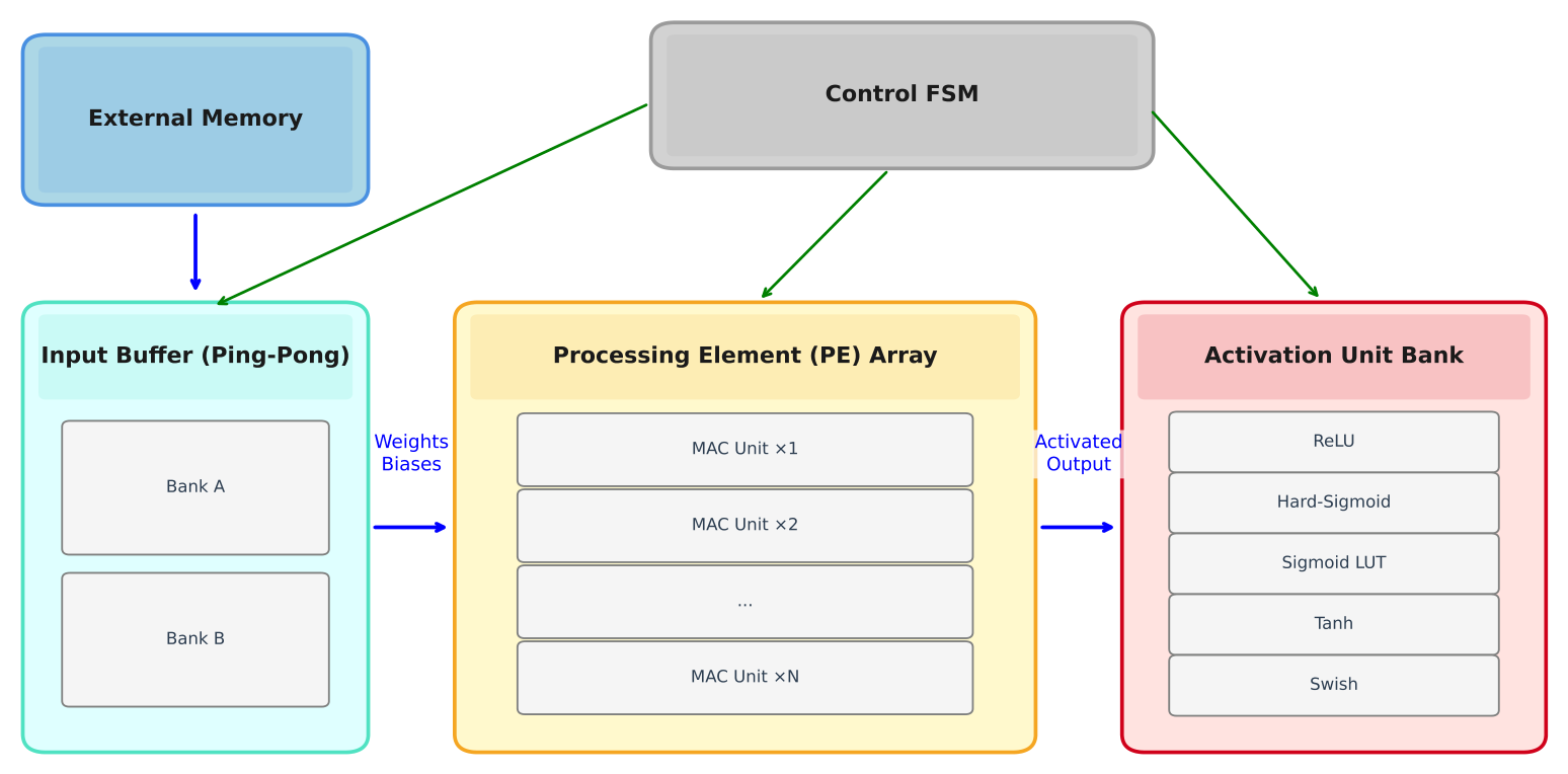
Figure 2.
Detailed RTL Datapath of the 3-stage pipelined MAC unit and the generic activation function generator.
Figure 2.
Detailed RTL Datapath of the 3-stage pipelined MAC unit and the generic activation function generator.
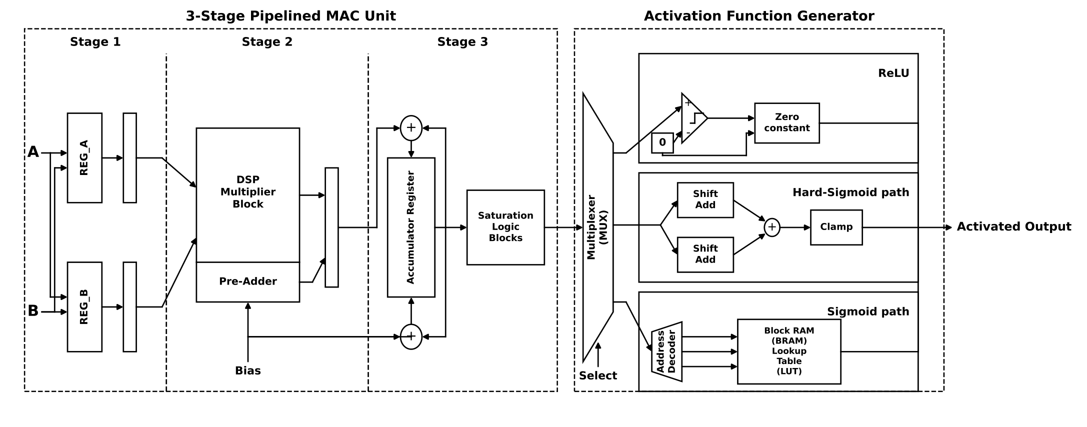
Figure 3.
Scheduling timing diagrams for (a) the Serial Processing Engine, showing the sequential iteration over 284 MAC operations, and (b) the Parallel Processing Engine, showing the spatially unrolled broadcast that completes the same computation in just 13 cycles.
Figure 3.
Scheduling timing diagrams for (a) the Serial Processing Engine, showing the sequential iteration over 284 MAC operations, and (b) the Parallel Processing Engine, showing the spatially unrolled broadcast that completes the same computation in just 13 cycles.
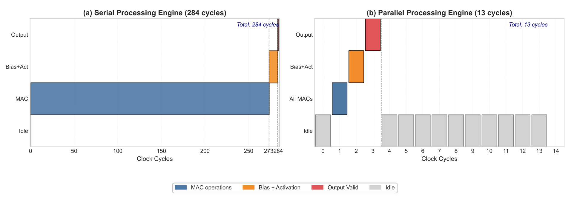
Figure 4.
Three-dimensional design-space exploration cube, showing the 18 hardware configurations synthesized. The axes represent Precision (Q8.8, Q12.12, Q16.16), Activation Function (ReLU, Sigmoid, Hard-Sigmoid), and Architecture Mode (Serial, Parallel).
Figure 4.
Three-dimensional design-space exploration cube, showing the 18 hardware configurations synthesized. The axes represent Precision (Q8.8, Q12.12, Q16.16), Activation Function (ReLU, Sigmoid, Hard-Sigmoid), and Architecture Mode (Serial, Parallel).
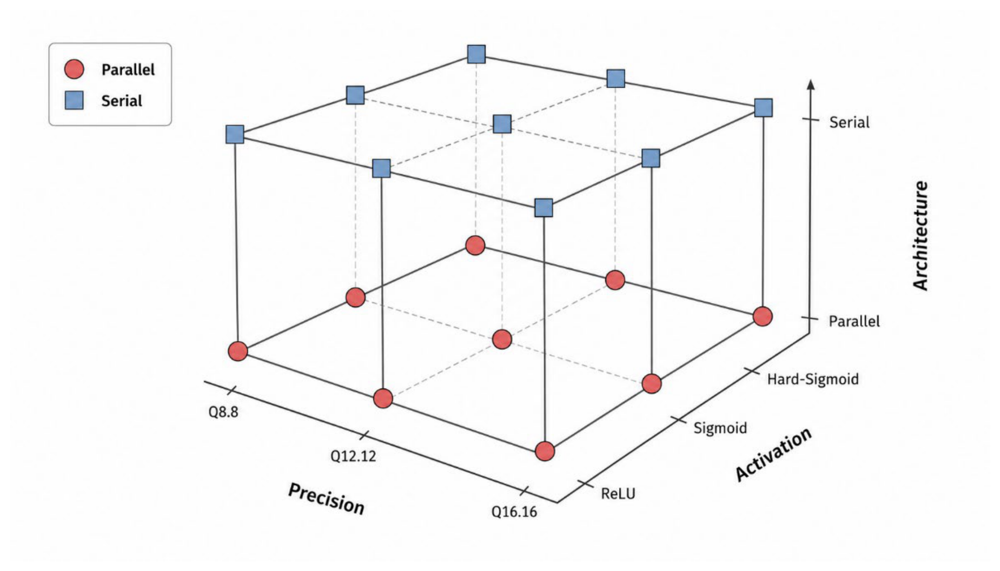
Figure 5.
Resource utilization heatmap for all 18 configurations. The x-axis groups configurations by Activation and Precision; the y-axis shows normalized LUT, FF, and DSP counts (scaled to the maximum observed value). Darker colors indicate higher utilization.
Figure 5.
Resource utilization heatmap for all 18 configurations. The x-axis groups configurations by Activation and Precision; the y-axis shows normalized LUT, FF, and DSP counts (scaled to the maximum observed value). Darker colors indicate higher utilization.
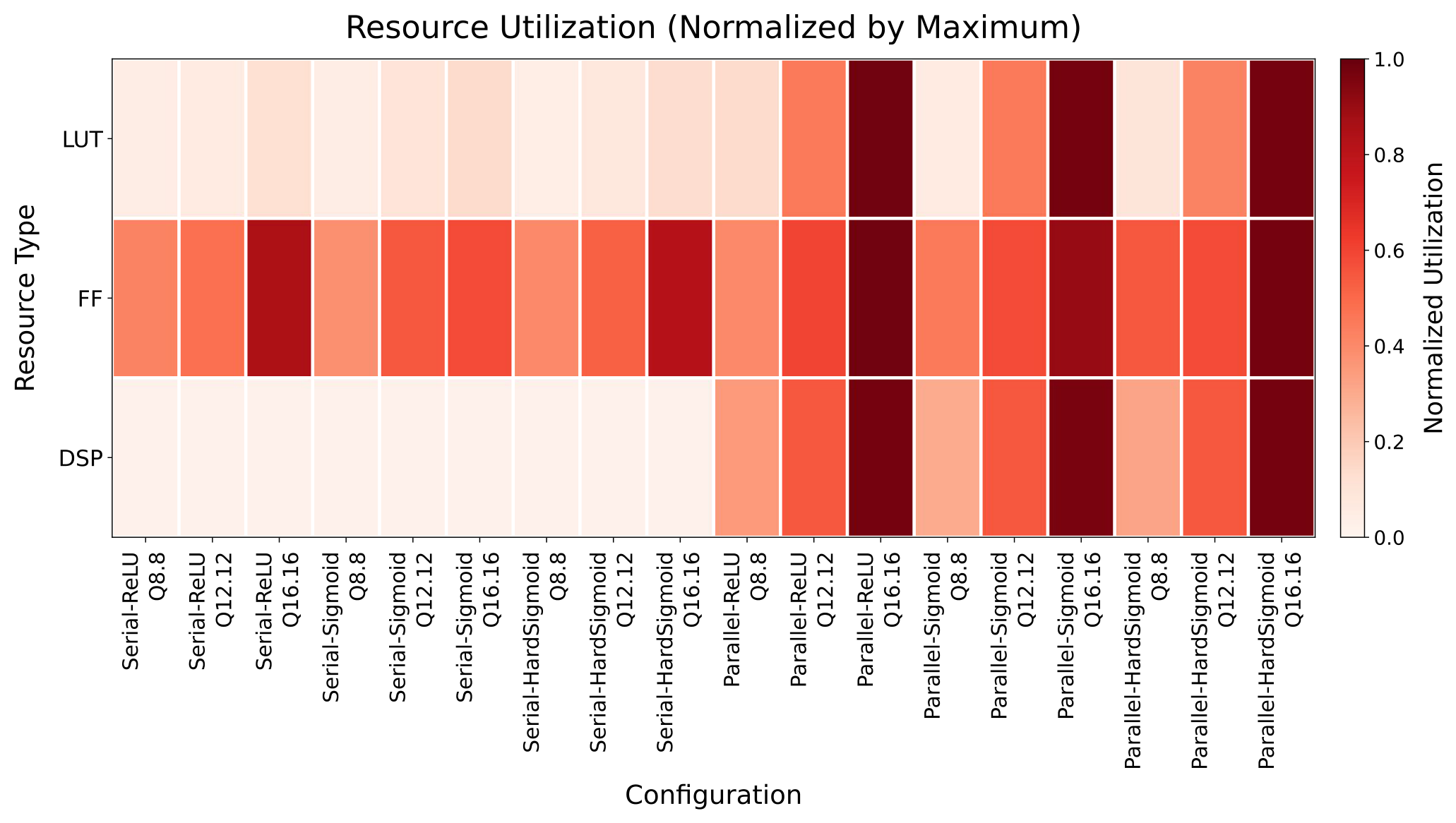
Figure 6.
Maximum frequency (F_{max}) as a function of precision for both Serial and Parallel architectures. The Serial curve shows the expected monotonic decrease with width. The Parallel curve exhibits a counter-intuitive “valley” at Q8.8 (58 MHz) and a “peak” at Q12.12 (106 MHz), confirming the critical-path shift from control logic to DSP chains.
Figure 6.
Maximum frequency (F_{max}) as a function of precision for both Serial and Parallel architectures. The Serial curve shows the expected monotonic decrease with width. The Parallel curve exhibits a counter-intuitive “valley” at Q8.8 (58 MHz) and a “peak” at Q12.12 (106 MHz), confirming the critical-path shift from control logic to DSP chains.
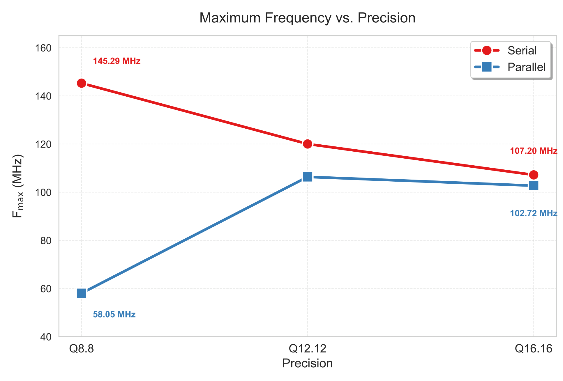
Figure 7.
Stacked bar chart comparing static (gray) and dynamic (colored) power dissipation for all nine Parallel configurations. The dynamic power grows exponentially with precision, while static power remains flat, confirming that leakage is device-bound and independent of our design.
Figure 7.
Stacked bar chart comparing static (gray) and dynamic (colored) power dissipation for all nine Parallel configurations. The dynamic power grows exponentially with precision, while static power remains flat, confirming that leakage is device-bound and independent of our design.
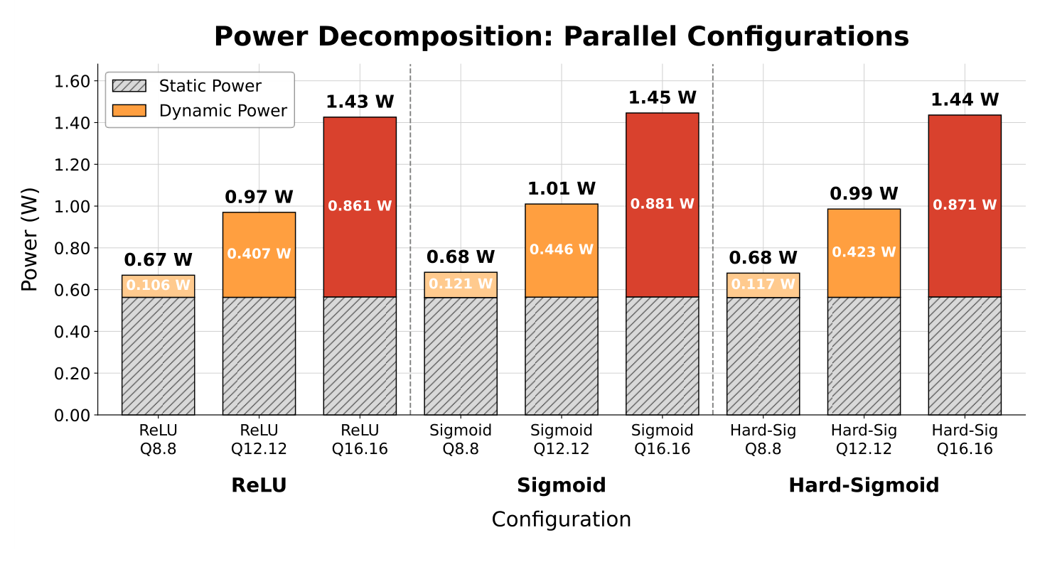
Figure 8.
Scatter plot of absolute Latency (cycles, log scale) vs. Throughput (MSps) for all configurations. Serial designs (blue) form a vertical cluster at 284 cycles with sub-1 MSps throughput. Parallel designs (red) form a cluster at 13 cycles, demonstrating throughputs exceeding 100 MSps, with Q12.12 providing an optimal balance within that cluster.).
Figure 8.
Scatter plot of absolute Latency (cycles, log scale) vs. Throughput (MSps) for all configurations. Serial designs (blue) form a vertical cluster at 284 cycles with sub-1 MSps throughput. Parallel designs (red) form a cluster at 13 cycles, demonstrating throughputs exceeding 100 MSps, with Q12.12 providing an optimal balance within that cluster.).
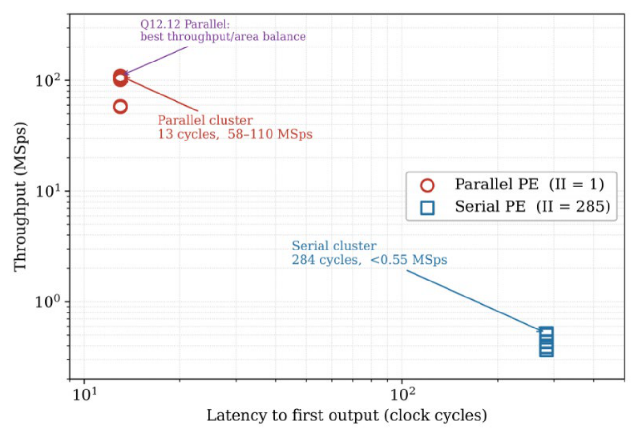
Figure 9.
Pareto scatter plot of Throughput (MSps) vs. Total Power (mW). Each point represents one configuration. The dashed red line indicates the Pareto frontier. Parallel Q12.12 ReLU (highlighted in green) sits on this frontier, proving it offers the best throughput for its power budget, whereas Q16.16 configurations lie strictly below the frontier (dominated).
Figure 9.
Pareto scatter plot of Throughput (MSps) vs. Total Power (mW). Each point represents one configuration. The dashed red line indicates the Pareto frontier. Parallel Q12.12 ReLU (highlighted in green) sits on this frontier, proving it offers the best throughput for its power budget, whereas Q16.16 configurations lie strictly below the frontier (dominated).
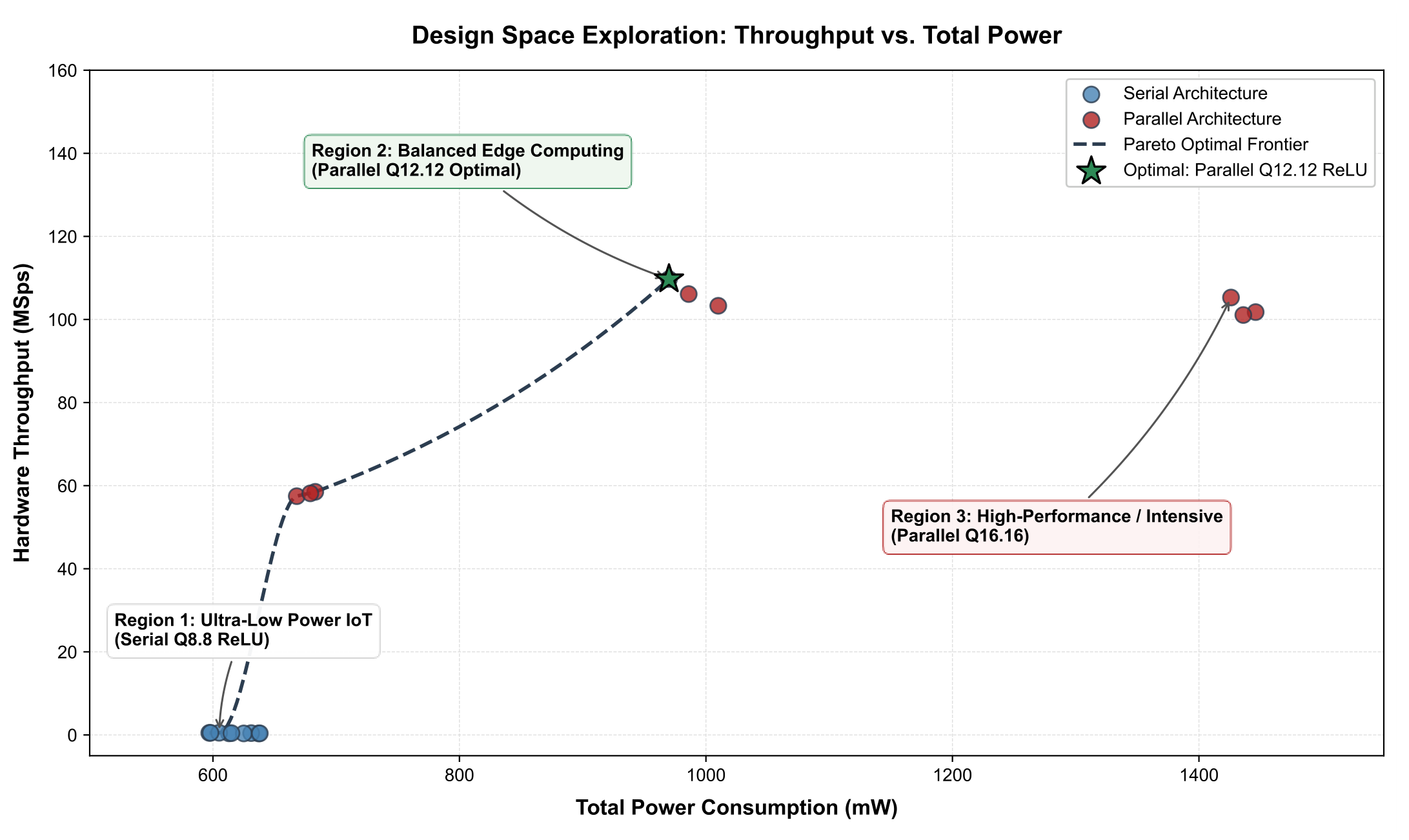
Figure 10.
Verification flow diagram showing the co-simulation framework. The MATLAB golden model generates test vectors (left), the VHDL testbench instantiates the DUT and interfaces via TEXTI/O (center), and the MATLAB post-processing script computes MSE and hardware accuracy (right).
Figure 10.
Verification flow diagram showing the co-simulation framework. The MATLAB golden model generates test vectors (left), the VHDL testbench instantiates the DUT and interfaces via TEXTI/O (center), and the MATLAB post-processing script computes MSE and hardware accuracy (right).
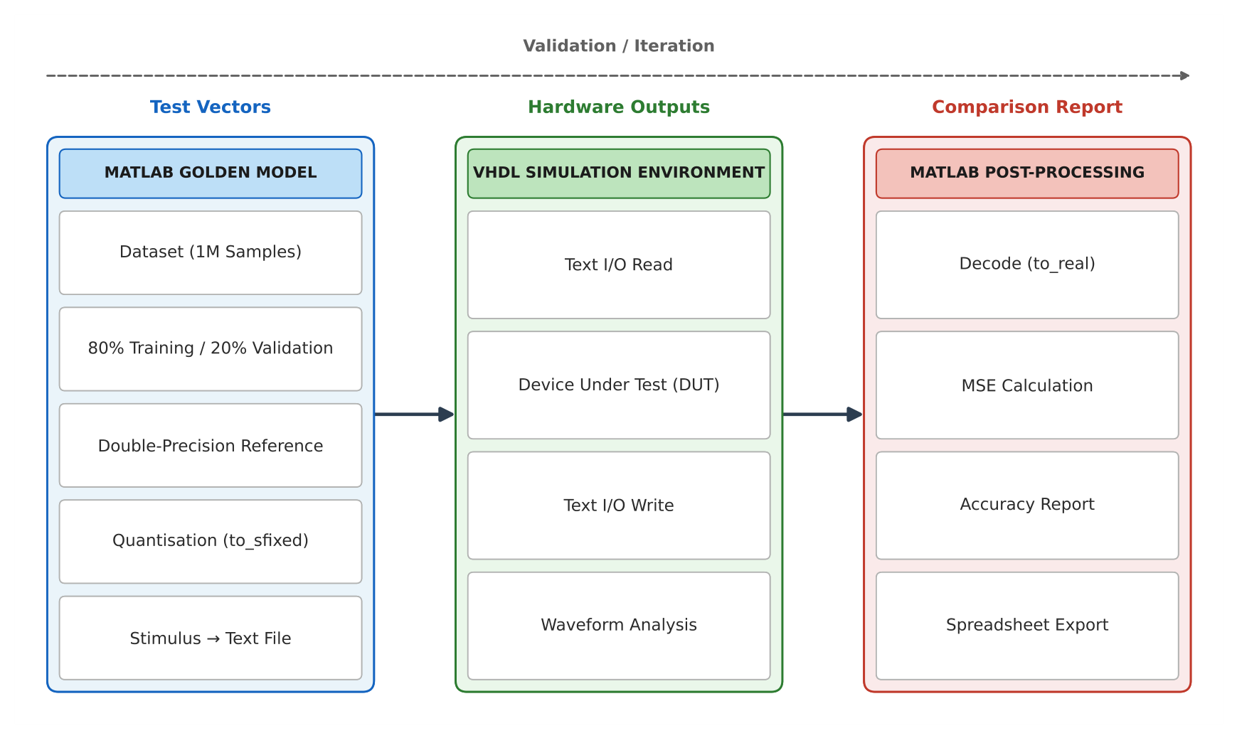

Table 1.
Performance and resource comparison of the proposed serial and parallel pe architectures across multiple precisions versus prior art.
Table 1.
Performance and resource comparison of the proposed serial and parallel pe architectures across multiple precisions versus prior art.
| Reference | FPGA Platform | Precision | Fmax (MHz) | throughput | DSPs | Accuracy loss |
|---|---|---|---|---|---|---|
| [3] | VC707 | FxP4/8/16/32 | 68 | 8.42 GOPS/W | N/A | <2% loss |
| [9] | ZYBO XC7020 | Q(2,14)-Q(32,32) | ~100 | 1.47 images/s | 54 | ~3% loss |
| [7] | Ultra96-V2 | 1-8 bit (mixable) | ~100 | Not reported | 32-128 | Not reported |
| [4] | VC707 | FP4/8, INT4, Posit-8/16 | N/A | Not reported | N/A | 0.6% loss (KALAM-16), 2.78% AF error |
| [8] | (ASIC, 45nm) | 4/8/16-bit int | 1 GHz | 1.92× over Stripes | N/A | 0% (bit ops only) |
| [6] | Ultra96-V2 | 2/4/8-bit | 250 | Not reported (AF only) | N/A | Up to 10% loss (PoT SiLU) |
| Our Design (Serial, Q8.8) | UltraScale+ xczu7ev | Q8.8 | 142.82 | 0.50 MSPS | 3 | <0.1% |
| Our Design (Parallel, Q16.16) | UltraScale+ xczu7ev | Q16.16 | 105.29 | 105.29 MSPS | 992 | <0.1% |
Fmax and resource values reported in the “Our Design” rows are based on the ReLU activation implementation to provide a consistent area/power baseline. For completeness, we also report that the peak Fmaxobserved across all evaluated activations is 148.13 MHz (Serial, Q8.8, Sigmoid), with a corresponding trade-off in LUT usage (1,887 LUTs in that Sigmoid configuration).
Table 2.
Precision Properties of the Evaluated Q_m.n Formats.
| Format | Total Bits (W) | Integer Bits (m) | Fractional Bits (n) | Dynamic Range | Resolution (2^(−n)) |
|---|---|---|---|---|---|
| Q8.8 | 16 | 8 | 8 | [−128, 127.9961] | 3.906 × 10(−3) |
| Q12.12 | 24 | 12 | 12 | [−2048, 2047.9998] | 2.441 × 10(−4) |
| Q16.16 | 32 | 16 | 16 | [−32768, 32767.99998] | 1.526 × 10(−5) |
Table 3.
Baseline Floating-Point Accuracy by Activation Function.
| Activation Function | Floating-Point Accuracy (%) | Correctly Classified Samples |
|---|---|---|
| Sigmoid | 99.868 | 199,736 |
| ReLU | 99.822 | 199,644 |
| Hard-Sigmoid | 99.589 | 199,178 |
| Leaky ReLU | 99.805 | 199,610 |
| Linear | 98.899 | 197,798 |
Table 4.
Fixed-Point Validation Accuracy and Precision Degradation.
| Activation Function | Q8.8 accuracy (%) | Q8.8 samples | Q12.12 accuracy (%) | Q12.12 samples | Q16.16 accuracy (%) | Q16.16 samples |
|---|---|---|---|---|---|---|
| Sigmoid | 99.784 | 199,568 | 99.872 | 199,744 | 99.869 | 199,738 |
| ReLU | 99.753 | 199,506 | 99.822 | 199,644 | 99.823 | 199,646 |
| Hard-Sigmoid | 99.543 | 199,086 | 99.592 | 199,184 | 99.589 | 199,178 |
| Leaky ReLU | 99.743 | 199,486 | 99.808 | 199,616 | 99.805 | 199,610 |
| linear | 98.871 | 197,742 | 98.898 | 197,796 | 98.899 | 197,798 |
Table 5.
Bit-growth and DSP mapping rules for the custom fixed-point package across the three explored precisions.
Table 5.
Bit-growth and DSP mapping rules for the custom fixed-point package across the three explored precisions.
| Parameter | Q8.8 | Q12.12 | Q16.16 |
|---|---|---|---|
| Integer Bits (Input) | 8 | 12 | 16 |
| Fractional Bits (Input) | 8 | 12 | 16 |
| Total Input Width | 16 | 24 | 32 |
| Multiplier Output (Wi + Wf) | 16 + 16 = 32 bits | 24 + 24 = 48 bits | 32 + 32 = 64 bits |
| Guard Bits | 4 | 4 | 4 |
| Accumulator Width | 36 bits | 52 bits | 68 bits |
| DSP Mapping per MAC | 1× DSP48E2 (synthesis-dependent) | multiple DSP48E2 slices (synthesis-dependent) | multiple DSP48E2 slices (synthesis-dependent) |
Table 6.
Hardware implementation strategy and resource cost for each activation function.
| Activation Function | Implementation Method | BRAM Cost | DSP Cost | LUT Cost (relative) |
| ReLU | Combinatorial comparator | 0 | 0 | Low |
| Hard-Sigmoid | Shift-add + clamp | 0 | 0 | Medium |
| Sigmoid | BRAM-based LUT (256×W) | 6.5 (36K blocks) | 0 | Low (adders only) |
Table 7.
Complete master synthesis results for all 18 implemented configurations. The highlighted rows (Q8.8 Parallel) show the anomalous Fmax plateau. Static power was constant at ~0.562 W across all runs and is omitted for brevity.
Table 7.
Complete master synthesis results for all 18 implemented configurations. The highlighted rows (Q8.8 Parallel) show the anomalous Fmax plateau. Static power was constant at ~0.562 W across all runs and is omitted for brevity.
| Mode | Activation | Precision | LUT | FF | DSP | BRAM | Fmax (MHz) | Dyn. Power (W) |
|---|---|---|---|---|---|---|---|---|
| Serial | ReLU | Q8.8 | 1,151 | 2,618 | 3 | 0 | 142.82 | 0.035 |
| Serial | ReLU | Q12.12 | 1,715 | 3,935 | 6 | 0 | 111.78 | 0.051 |
| Serial | ReLU | Q16.16 | 2,247 | 5,236 | 12 | 0 | 105.04 | 0.075 |
| Serial | Sigmoid | Q8.8 | 1,887 | 2,118 | 3 | 6.5 | 148.13 | 0.043 |
| Serial | Sigmoid | Q12.12 | 3,725 | 3,160 | 6 | 12.5 | 124.88 | 0.069 |
| Serial | Sigmoid | Q16.16 | 4,016 | 4,061 | 12 | 12.5 | 105.25 | 0.090 |
| Serial | Hard-Sigmoid | Q8.8 | 2,158 | 2,568 | 3 | 0 | 144.93 | 0.036 |
| Serial | Hard-Sigmoid | Q12.12 | 3,005 | 3,885 | 6 | 0 | 123.47 | 0.052 |
| Serial | Hard-Sigmoid | Q16.16 | 3,932 | 5,186 | 12 | 0 | 111.30 | 0.076 |
| Parallel | ReLU | Q8.8 | 1,409 | 2,019 | 273 | 0 | 57.47 | 0.106 |
| Parallel | ReLU | Q12.12 | 9,710 | 4,577 | 496 | 0 | 109.72 | 0.407 |
| Parallel | ReLU | Q16.16 | 23,916 | 6,375 | 992 | 0 | 105.29 | 0.861 |
| Parallel | Sigmoid | Q8.8 | 2,119 | 1,519 | 273 | 6.5 | 58.52 | 0.121 |
| Parallel | Sigmoid | Q12.12 | 11,619 | 3,798 | 496 | 12.5 | 103.30 | 0.446 |
| Parallel | Sigmoid | Q16.16 | 22,135 | 5,200 | 992 | 12.5 | 101.78 | 0.881 |
| Parallel | Hard-Sigmoid | Q8.8 | 2,464 | 1,969 | 273 | 0 | 58.15 | 0.117 |
| Parallel | Hard-Sigmoid | Q12.12 | 10,978 | 4,527 | 496 | 0 | 106.12 | 0.423 |
| Parallel | Hard-Sigmoid | Q16.16 | 23,136 | 6,325 | 992 | 0 | 101.08 | 0.871 |
Table 8.
Critical path source decomposition for parallel and serial modes. The Q8.8 parallel bottleneck is clearly non-arithmetic, confirming the shared FSM is the limiting factor.
Table 8.
Critical path source decomposition for parallel and serial modes. The Q8.8 parallel bottleneck is clearly non-arithmetic, confirming the shared FSM is the limiting factor.
| Architecture | Precision | Critical Path Source | Observed Fmax (MHz) |
|---|---|---|---|
| Parallel | Q8.8 | Control FSM + Address Decoder (combinatorial mux fan-out) | ~58 |
| Parallel | Q12.12 | DSP Multiplier Chain (internal arithmetic routing) | ~106 |
| Parallel | Q16.16 | DSP Cascaded Chain (CARRYCASC path) | ~105 |
| Serial (all) | Q8.8 / Q12.12 / Q16.16 | Adder Carry Chain (varies with data width) | 148 → 105 |
Table 9.
Throughput, power, and energy efficiency comparison for q12.12 parallel implementations across activation functions.
Table 9.
Throughput, power, and energy efficiency comparison for q12.12 parallel implementations across activation functions.
| Rank | Configuration | Throughput (MSps) | Total Power (W) | Efficiency (MSps/W) |
|---|---|---|---|---|
| 1 | Parallel Q12.12 ReLU | 109.72 | 0.97 | 113.1 |
| 2 | Parallel Q12.12 Hard-Sigmoid | 106.12 | 0.988 | 107.6 |
| 3 | Parallel Q12.12 Sigmoid | 103.3 | 1.01 | 102.3 |
Disclaimer/Publisher’s Note: The statements, opinions and data contained in all publications are solely those of the individual author(s) and contributor(s) and not of MDPI and/or the editor(s). MDPI and/or the editor(s) disclaim responsibility for any injury to people or property resulting from any ideas, methods, instructions or products referred to in the content. |
© 2026 by the authors. Licensee MDPI, Basel, Switzerland. This article is an open access article distributed under the terms and conditions of the Creative Commons Attribution (CC BY) license (http://creativecommons.org/licenses/by/4.0/).
Copyright: This open access article is published under a Creative Commons CC BY 4.0 license, which permit the free download, distribution, and reuse, provided that the author and preprint are cited in any reuse.