

Submitted:
08 September 2026
Posted:
09 September 2026
You are already at the latest version
Abstract
Among commercially available enhancement-mode GaN devices, Schottky-type p-GaN gate HEMTs have emerged as the dominant device architecture owing to their excellent gate-drive compatibility and low gate-drive losses. With their superior switching speed and power density over silicon MOSFETs, these devices have become ubiquitous in consumer electronics and are now extending into high-reliability industrial power conversion. However, their limited Short-Circuit (SC) robustness remains a major barrier to such applications. This article systematically reviews the current understanding of the short-circuit reliability of Schottky-type p-GaN HEMTs. Particular attention is devoted to: (1) an overview of the attainable SC capability and the associated failure modes and mechanisms; (2) SC instability, including the underlying degradation mechanisms and physical models; and (3) chip-level approaches for intrinsically enhancing SC robustness. This review provides a unified framework for understanding the fundamental mechanisms governing the SC reliability of Schottky-type p-GaN HEMTs, offering valuable physical insights and a theoretical basis for the development of intrinsically robust GaN power devices. It also serves as a useful reference for SC reliability qualification and the deployment of GaN power transistors in demanding power conversion applications.
Keywords:
p-gallium nitride (GaN) gate high electron mobility transistors (HEMTs)
; short-circuit reliability
; degradation mechanism
; short circuit failure
; chip-level hardening techniques
1. Introduction
The relentless pursuit of higher switching frequencies and power densities in modern power electronics is continually approaching the intrinsic material limits of silicon-based devices, such as the breakdown electric field and carrier mobility [1]. Consequently, wide-bandgap semiconductors, particularly Silicon Carbide (SiC) and Gallium Nitride (GaN), have rapidly emerged in both commercial markets and academic research as promising alternatives for next-generation power conversion systems. Among them, GaN, owing to its wide bandgap (3.4 eV) and high electron saturation velocity, enables substantially higher switching speeds, conversion efficiencies, and power densities than conventional silicon devices [1,2,3]. To capitalize on these material advantages, the Schottky-type p-GaN gate HEMT has emerged as the dominant commercial GaN power-device architecture owing to its normally-off operation, excellent gate-drive compatibility, and low gate-drive losses. It has achieved widespread adoption in consumer electronics[4,5,6,7], and is now being actively pursued for industrial applications including data centers[8], photovoltaic inverters[9], and electric vehicles[10,11,12].Nevertheless, industrial power conversion systems impose stringent requirements on device reliability and long-term stability, with only limited parameter degradation being acceptable during operation. The present reliability performance of Schottky-type p-GaN HEMTs has yet to fully satisfy these demands, thereby hindering their large-scale deployment in high-reliability applications. In fact, SC ruggedness is widely acknowledged as one of the most critical figures of merit for power semiconductor devices. In practical high-power converter systems, an SC fault subjects the device to the simultaneous presence of high current and high voltage, constituting an accidental and extremely severe electrothermal stress. Three types of SC faults are commonly encountered: type-I hard-switching fault (HSF), type-II fault-under-load (FUL), and type-III flashover fault (FOF) [13,14,15]. In an HSF event, the device abruptly transitions from the OFF state to the SC state, as may occur in a half-bridge leg owing to an erroneous gate signal. In contrast, FUL results from a load-side failure while the device is conducting, whereas FOF is triggered by insulation breakdown within the power system, leading to exceptionally high di/dt and dv/dt transients [14,16]. These fault conditions can induce severe degradation or catastrophic failure, thereby jeopardizing the safe operation of the entire power system. Generally, the vast majority of reported studies have adopted the type-I HSF configuration for SC reliability evaluation because it provides a well-controlled drain-voltage stress, allows convenient gate-signal control and fault initiation, and closely emulates practical operating conditions. Moreover, experimental results reported by EPC indicate that the SC withstand capability does not differ significantly between HSF and FUL conditions [17]. To date, research on the SC ruggedness of p-GaN HEMTs has mainly focused on three areas: the attainable SC capability together with the associated failure modes and critical influencing factors [18,19,20,21,22,23,24,25,26,27,28,29,30], SC-induced degradation and the corresponding physical models [31,32,33,34,35,36,37,38,39], and chip-level SC hardening techniques [40,41,42,43,44,45,46]. However, a comprehensive review that not only summarizes these findings but also provides a unified perspective on the underlying reliability physics and their interrelationships is still lacking. Therefore, a systematic review of the SC ruggedness of Schottky-type p-GaN HEMTs is of both significant scientific interest and practical importance for the development and qualification of reliable GaN power devices. This paper is organized as follows. Section 2 reviews the SC withstand capability of Schottky p-GaN HEMTs under both single- and repetitive-pulse stress. The distinct failure modes associated with these two operating conditions are discussed. In particular, two representative thermal failure modes under single-pulse SC stress are compared, whereas repetitive SC stress is shown to generate substantial cyclic mechanical stress through thermal expansion and contraction of the GaN epitaxial layers. Section 3 addresses SC-induced instability and degradation. Monotonic shifts in threshold voltage (Vth) and on-resistance (Ron), typically observed in low-voltage devices, are attributed to electron trapping, whereas high-voltage Schottky p-GaN HEMTs exhibit unique nonmonotonic degradation due to the interplay between electron trapping and thermally enhanced hole injection. Section 4 surveys chip-level SC hardening strategies, including gate–source topology innovations and barrier, surface engineering approaches. Both conventional current-limiting techniques and recently developed adaptive protection concepts based on transient-gate-current-induced gate-voltage feedback are discussed, together with representative implementations in GaN and SiC power devices.
2. Short-Circuit Capability and Failure Mechanisms of Schottky p-GaN HEMTs
2.1. Short-Circuit Capability of p-GaN HEMTs
SC ruggedness is one of the essential reliability metrics for power devices in power conversion systems and is commonly evaluated in terms of both single-pulse and repetitive-pulse SC capability. For single-pulse SC operation, the Short-Circuit Withstand Time (SCWT) is the primary figure of merit. It is defined as the duration from the occurrence of a short-circuit fault to catastrophic device failure. Therefore, the SCWT must be sufficiently long to allow the protection circuitry to detect the fault and safely shut down the device before irreversible damage occurs, thereby ensuring the reliable operation of the power system. Consequently, a minimum SCWT of approximately 10μs under a 400-V DC bus has become a widely accepted benchmark for 650-V-class power devices [18]. In addition to single-pulse capability, repetitive SC endurance is another key metric for evaluating SC capability. It is commonly quantified by the maximum number of SC cycles that a device can survive under specified SC conditions. State-of-the-art commercial Si IGBTs, for example, can typically withstand more than 1000 repetitive SC cycles with a pulse width of 10μs [45,46,47]. Such repetitive SC capability is also significant for improving system robustness by tolerating multiple accidental SC events throughout the converter lifetime.
Owing to their unique gate structure and polarization-induced 2DEG conduction mechanism, the SC behavior of GaN HEMTs differs distinctly from that of conventional Si power devices. Consequently, the reliability theories established for Si devices cannot be directly applied to GaN HEMTs, motivating extensive studies on their SC behavior and capability. Table 1 summarizes selected published experimental studies on the short-circuit withstand capability of commercial 650-V GaN HEMT. The included studies cover both depletion-mode (D-mode) and p-GaN gate enhancement-mode (E-mode) devices, as well as both single-pulse SCWT and repetitive short-circuit reliability characterization. Non-commercial devices and purely simulation-based studies are outside the scope of this table. It can be seen that commercially available GaN HEMTs generally exhibit a very limited SC capability. For single-pulse, Similarly, repetitive-pulse SC capability of GaN HEMTs remains severely limited. As listed in Table 1, both 650 V p-GaN gate HEMTs failed at merely the second SC pulse under VDS = 400 V and VGS = 6 V, irrespective of whether the single-pulse duration was 1μs [27] or 10μs [31]. This repetitive SC capability is markedly inferior to that of Si IGBTs. To further elucidate the factors governing SC capability, some studies have systematically also investigated the influence of different SC stress conditions. Experimental results consistently demonstrate that the SC capability is primarily affected by the drain bias VDS [18], gate bias VGS [18,33], external gate resistance RG [26], and the peak short-circuit current Ids, peak [24] during the SC event. Specifically, for 650-V GaN HEMTs, the SCWT decreases drastically from >20μs at VDS = 250 V to <0.5μs at VDS = 400 V, identifying the drain bias as the most critical factor [18]. Reducing VGS from 6 V to 4 V enables the device to withstand a 10-μs SC stress at a 400-V bus voltage, confirming the effectiveness of lowering gate overdrive in limiting SC current [34]. In terms of gate resistance, increasing RG from 10 Ω to 47 Ω extends the single-pulse SCWT of p-GaN HEMTs from 630μs to 982μs (a 56% improvement) [26]. Moreover, a negative correlation between the Ids, peak and SCWT has been established, revealing that devices with the lowest Ids, peak exhibit the longest SC endurance [24]. These observations consistently indicate that the SC capability is fundamentally determined by the electrothermal energy accumulated during the SC event. Based on these observations, the underlying SC failure mechanisms under both single-pulse and repetitive-pulse stress have been systematically investigated. These studies establish the fundamental physical basis for understanding SC failure and provide theoretical guidance for improving the SC ruggedness of GaN HEMTs.
2.2. Thermal Runaway and Material Melting Driven By Single-pulse SC Tests
Schottky-type p-GaN HEMTs exhibit two distinct single SC failure modes, which differ significantly in dissipated energy (ESC), SCWT, and damage morphology. The first mode typically occurs at relatively lower drain-source voltages and is characterized by a longer failure time, higher dissipated energy, and larger catastrophic chip-scale damage. In contrast, the second mode is triggered at higher drain-source voltage, resulting in a much shorter time-to-failure, lower ESC, and highly localized damage beneath the source field plate near the drain-side gate edge. Despite these distinct failure characteristics, both modes are fundamentally governed by the same thermal criterion: the local device temperature exceeds a material-dependent critical threshold during short-circuit operation. [19,20,22].
For the high-voltage failure mode, however, the critical temperature is reached through highly localized electrothermal overstress rather than global heat accumulation. The failure waveform is shown in Figure 1, this failure mode is characterized by an ultrashort failure time (<1μs), a low ESC of only a few millijoules, yet an extremely high transient power approaching 10 kW under VGS≥ 4.5V and VDS ≥300 V [20]. Figure 2 presents the corresponding failure morphology at progressively higher magnifications. The decapsulated device shown in Figure 2a reveals only a small damaged region near the drain side, while the enlarged views in Figure 2b and Figure 2c further confirm that the damage is confined beneath the source field plate adjacent to the drain-side gate edge, indicating a highly localized thermal failure. Consistently, failure analysis and TCAD simulations reveal that the maximum lattice temperature is always concentrated at this location, as illustrated in the TCAD simulation results shown in Figure 3. The localized failure originates from the coupling of electric-field and current-crowding effects. Under high-drain short-circuit bias, pronounced electric-field peaks develop at the drain-side gate edge, while the electron current density increases significantly within the narrow channel beneath the source field plate and gate filed plate. Furthermore, the asymmetric chip layout aggravates current crowding at the chip level, reducing the effective active area by approximately 8% at VDS = 360 V and 15% at VDS = 485 V (VGS = 4.5 V) [22]. The resulting ultrahigh local power density rapidly drives the junction temperature beyond the critical thermal limit of the GaN/AlGaN heterostructure, ultimately leading to catastrophic failure.
In contrast, under low drain-voltage conditions, the longer SC duration results in substantially higher energy dissipation, making global heat accumulation the dominant failure mechanism [26]. The failure waveform is shown in Figure 4. For example, at VDS = 250 V and VGS=5V, the device fails after about 380μs with a calculated energy of about 260 mJ, and the junction temperature is estimated to reach about 525 °C [20]. The resulting failure morphology is illustrated in Figure 5. As shown in Figure 5a, two large melted regions are observed near the drain metallization, indicating severe chip-level thermal damage. The enlarged views in Figure 5b further reveal that Region A extends vertically over approximately 200μm, while Region B exhibits a lateral width of about 70μm [19]. Unlike the localized failure observed under high drain bias, this failure mode originates from global heat accumulation throughout the device. Owing to the relatively high thermal resistance of the buffer layer [22], the generated heat cannot be efficiently dissipated during the prolonged SC stress. Meanwhile, chip-level current nonuniformity causes preferential heat generation near the drain metallization [20], where the temperature eventually exceeds the melting point of the surface metal. Consequently, extensive metallization melting and large-area thermal damage are induced, ultimately leading to catastrophic device failure.
2.3. Electrothermal Cumulative Failure Under Repetitive SC Stress
Compared with single-pulse SC failure, repetitive SC failure follows a distinct thermomechanical degradation process before catastrophic thermal failure occurs. Although both failure modes ultimately result in thermal destruction, repetitive SC failure is induced by the cumulative effect of cyclic electrothermal stress rather than a single extreme thermal event. Consequently, the repetitive SC ruggedness of p-GaN HEMTs is significantly inferior to their single-pulse SC ruggedness, with device failure occurring after substantially lower cumulative dissipated energy. Experimental investigation in [24] revealed that repetitive SC failure is governed by a cumulative dissipated-energy threshold rather than a fixed number of SC cycles. For the investigated 650-V Schottky-type p-GaN HEMT, failure occurred after only two repetitive SC pulses under VDS=400 V and VGS=5V, and a pulse width of 500 ns, corresponding to a cumulative dissipated energy of approximately 20 mJ[24].
The irreversible failure of p-GaN HEMTs under repetitive SC stress originates from a progressive thermomechanical degradation process induced by cyclic electrothermal loading. Owing to the unique GaN-on-Si heterostructure, the transition layer and SiN passivation layer possess substantially lower thermal conductivity than the AlGaN/GaN epitaxial layers [27,28]. Consequently, the heat generated during each SC pulse is confined within the thin GaN channel and buffer region, producing a pronounced transient temperature spike (Figure 6). Rather than directly triggering catastrophic thermal failure as in single-pulse SC events, the repeated temperature rise and subsequent cooling during successive SC cycles induce cyclic thermal expansion and contraction within the heterostructure, resulting in the gradual accumulation of thermomechanical stress as confirmed by the simulated stress distribution in Figure 7. The resulting thermomechanical stress progressively initiates and propagates thermal-fatigue cracks at the interface between the GaN buffer layer and the transition layer. As the cyclic thermomechanical stress accumulates, thermal-fatigue cracks are progressively initiated and propagated at the mechanically vulnerable interface between the GaN buffer layer and the transition layer [27,28]. As illustrated in Figure 8a, cracks develop between the second field-plate edge and the drain electrode after repetitive SC stress. The cross-sectional image in Figure 8b further reveals that the crack center is located precisely at the GaN buffer layer–transition layer interface, confirming that cyclic thermomechanical fatigue is the dominant physical origin of structural degradation. The progressive structural degradation further deteriorates the thermal dissipation capability of the device. Transient thermal-resistance characterization [29] indicates that the combined action of large temperature gradients and electrical stress promotes the generation of dislocations within the nucleation and buffer layers. The accumulated defects increase the thermal boundary resistance and overall thermal impedance, thereby suppressing vertical heat dissipation. Consequently, an increasing fraction of the generated heat remains confined within the active region during subsequent SC cycles, leading to progressively higher junction temperatures. The aggravated heat accumulation further accelerates thermomechanical degradation, establishing a self-reinforcing electrothermal feedback loop that ultimately culminates in premature thermal runaway and catastrophic device failure.
3. Degradation Under Repetitive Short-Circuit Stress
The previous section focused on the failure mechanisms of Schottky-type p-GaN HEMTs under single-pulse and repetitive SC stress. Besides possessing sufficient SC withstand capability, power devices must also maintain stable electrical characteristics during repetitive SC events to ensure the long-term reliability and safe operation of power conversion systems. However, repetitive electrothermal stress inevitably induces gradual electrical parameter degradation, particularly in the Vth, drain saturation current (IDS) and Ron. Such electrical instability degrades the gate-drive margin, increases the conduction and switching losses, and ultimately compromises system reliability. Accordingly, extensive studies have investigated the evolution of electrical parameters under repetitive SC stress and established the corresponding degradation mechanisms. This section reviews the repetitive SC degradation behavior, the associated electrical instability, and the underlying physical mechanisms.
3.1. Electrical Instability Under Repetitive SC Stress
The repetitive SC stability of p-GaN HEMTs is also commonly evaluated using a hard-switching SC test platform. The test circuit and corresponding gate-drive timing are illustrated in Figure 9. During the evaluation, repetitive SC pulses are applied while ensuring that the device operates within its short-circuit safe operating area (SCSOA). An SC stress–electrical characterization–SC stress methodology is generally adopted, in which the repetitive SC test is periodically interrupted to characterize the electrical parameters of the device using a semiconductor parameter analyzer (e.g., Keysight B1505A). The degradation of key electrical parameters, including the Vth, Ron, is then monitored as a function of SC stress conditions and SC cycle count. Existing studies indicate that the electrical instability of p-GaN HEMTs under repetitive SC stress can generally be classified into two categories. The first is monotonic degradation, which is predominantly reported in low- and medium-voltage devices (rated at 100V), where the degradation continuously accumulates with increasing SC stress level and cycle count. The second is non-monotonic bidirectional degradation, which has recently been observed mainly in high-voltage p-GaN HEMTs (rated at 650V). The following sections review these two degradation behaviors and their underlying physical mechanisms.
Previous systematic studies have revealed a monotonic degradation behavior in low-voltage p-GaN HEMTs under repetitive SC stress. As shown in Figure 10, the Vth increases monotonically and the Ron similarly exhibits an upward trend with increasing SC cycle count, VGS, and VDS [35]. Notably, the most pronounced degradation generally occurs after the first SC event, followed by a progressively saturated evolution with further SC cycling. Moreover, increasing the SC stress severity, including higher VGS and VDS, leads to larger positive Vth shifts, greater Ron degradation, indicating a strong correlation between electrical parameter degradation and SC stress intensity. Similar monotonic degradation characteristics have also been observed in high-voltage p-GaN HEMTs under relatively mild SC stress conditions [31], suggesting that the same degradation mechanism dominates when the electrothermal stress remains limited.
In contrast to the monotonic degradation observed in low-voltage devices, high-voltage Schottky-type p-GaN HEMTs have recently been reported to exhibit a distinctly non-monotonic degradation behavior under repetitive SC stress [31]. As shown in Figure 11, the electrical parameters initially follow the conventional positive degradation trend but gradually reverse with increasing SC count and higher VDS, VGS. Specifically, Vth first shifts positively after the initial SC events and subsequently drifts in the negative direction with continued SC cycling, accompanied by a significant attenuation of the Ron degradation. For example, under relatively mild SC stress (650V device, VGS = 4 V, VDS = 100 V), ΔVth reaches approximately +0.69 V after 10 SC cycles. However, under higher SC stress (650V device, VGS = 6 V, VDS = 300 V), ΔVth decreases to only 0.04 V after 100 SC cycles, while the increase in Ron is reduced to merely 3% [31]. Such bidirectional parameter evolution suggests that the degradation mechanism of high-voltage p-GaN HEMTs fundamentally differs from the monotonic degradation observed in low-voltage devices.
3.2. Physical Mechanisms of Vth and Ron Degradation
During a SC event, the p-GaN gate HEMT simultaneously withstands a high bus voltage and a large current, so that two extreme physical conditions coexist inside the device: localized high peak electric fields at the drain-side gate edge and the field-plate edge, and severe self-heating caused by the rapid dissipation of the Esc. These two conditions respectively drive two carrier-trapping processes of opposite polarity: field-assisted hot-electron trapping accumulates net negative charge in the gate stack and the drift region, leading to a positive drift of the Vth and an increase in the on-resistance Ron; whereas thermally enhanced hole injection introduces positive charge into the AlGaN/GaN heterostructure, neutralizing the negative-charge accumulation in the gate stack and thereby weakening or even reversing the Vth drift; concurrently, the elevated junction temperature suppresses hot-electron generation and electron trapping, alleviating the degradation of Ron. Their competition gives rise to the distinctive non-monotonic instability of Vth and Ron with SC stress intensity in 650 V Schottky-type p-GaN gate HEMTs [31].
Under mild repetitive SC stress (for a 650 V device with VDS < 100 V and VGS < 4 V), the short-circuit energy is low and the self-heating is moderate; the localized high peak electric field is the fundamental driving factor of degradation. The physical picture is illustrated in Figure 12: the positive gate bias bends the energy bands of the gate stack downward, forming a high-density 2DEG in the channel; during the SC event, electrons are accelerated by the high peak electric field at the drain-side gate edge into hot electrons and spill over the channel; part of these hot electrons are captured by traps in the p-GaN/AlGaN gate stack, and the negatively charged occupied traps deplete the 2DEG, resulting in a positive drift of Vth. Meanwhile, the high electric field at the source field plate (SFP) edge assists the transfer of electrons from the 2DEG channel and their capture at the residual dielectric/AlGaN interface states, producing a virtual-gate-like effect that increases Ron [31]. The magnitude of degradation in this regime should not be overlooked: for 650V device at VGS = 4 V and VDS = 100 V, after 100 cycles Vth drifts from 1.27 V to 1.95 V and Ron increases by about 34.5%; even a single SC event can cause a +0.40 V Vth shift and an 11% increase in Ron, which is sufficient to significantly degrade the dead time and conduction loss in practical applications [31]. It is worth noting that, although earlier degradation studies on low-voltage (≤100 V-class) devices reported only monotonic positive drift, their mechanistic explanations can be uniformly incorporated into the mild-stress framework described above.
When the repetitive SC stress exceeds a certain critical intensity ( for a 650 V device with VDS ≥100 V and VGS>4 V), the degradation mechanism of the device undergoes an essential transition, as shown in Figure 13. In the hole-injection-dominated regime, a higher gate stress voltage (4 V < VGS ≤ 6 V) triggers hole injection from the p-GaN layer into the AlGaN/GaN heterostructure at the source-side gate edge—where the electric field induced by the SC gate stress voltage points approximately perpendicularly toward the 2DEG channel, lowering the local valence-band barrier; by contrast, the drain-side gate edge is dominated by the high SC drain stress voltage, and the valence-band barrier is much higher, as comparatively shown in Figure 13a. At the same time, as show in Figure 14 the strong self-heating triggered by the SC event raises the junction temperature in the gate region considerably, and the elevated temperature effectively may activate the ionization of acceptors in the p-GaN layer, further amplifying hole injection. The injected holes are subsequently captured by traps in the AlGaN barrier layer and the GaN buffer, reducing the net negative charge stored in the gate stack.
4. Short-Circuit Hardening Strategies for Schottky p-GaN Devices
4.1. Current-Limiting Device Engineering for Short-Circuit Hardening
Since catastrophic SC failure in p-GaN HEMTs is primarily caused by excessive power dissipation and the resulting thermal runaway, one of the most established hardening strategies is to intrinsically suppress the SC current through structural engineering. This design philosophy has been widely adopted in Si and SiC power devices and has recently been extended to p-GaN HEMTs. By reducing the saturation drain current IDS, the peak SC current Ids,peak and the corresponding peak power dissipation are effectively suppressed, thereby mitigating thermal accumulation during SC events and significantly improving both the single-pulse SC withstand capability and repetitive SC reliability. Several structural designs have been proposed to realize this intrinsic current-limiting effect without relying on external protection circuits. Rather than introducing a single universal solution, these approaches modify different regions of the device to regulate channel conduction under SC conditions while maintaining acceptable on-state performance.
One representative approach is the Schottky source extension (SSE), which is is integrated into the source side of the device; Figure 15 presents the schematic structures of the conventional device and the proposed device and equivalent circuit of the p-GaN HEMT integrated with the SSE. Under low drain bias, the SSE functions equivalently as a small series resistance and exerts minimal suppression on channel conduction. However, as the VDS increases, the potential at the SSE node (VX) rises rapidly. Once VX reaches the drain saturation voltage of the channel beneath the SSE, this region becomes pinched off and the extension behaves as a constant-current source. As a result, the saturation current decreases from more than 400 mA/mm in the conventional device to approximately 100 mA/mm in the SSE-integrated device, as shown in Figure 16. Consequently, the saturation drain current is intrinsically limited, thereby suppressing the peak SC current and instantaneous power dissipation. AS shown in Figure 17a–d, high-voltage pulse ID–VDS tests, which mimic SC events with a 5-ms pulse width and VGS held at 6 V, reveal that the conventional device fails at 351 V, whereas the SSE device withstands drain voltages up to 679 V. Progressive SC-stress characterization further shows that the conventional device fails under repeated stresses at 300 V, while the SSE device endures cumulative stresses up to 700 V before failure. Moreover, under repetitive SC cycling tests at VDS = 400 V, VGS = 6 V, and 10-μs pulse width, the conventional device fails after only approximately 3,064 cycles, whereas the SSE device operates stably for 11,571 cycles. These results demonstrate that the SSE structure substantially enhances both the SC withstand voltage and the repetitive SC durability.
As shown in Figure 18a, another on-chip current-limiting technique involves inserting a second gate between the main gate and the drain and shorting it to the source. As shown in Figure 18b, when large drain current flows through the source resistance during an SC event, the potential at the location beneath the second gate in the channel rises, while the second gate remains at zero potential due to its direct connection to the source. A negative bias thus develops between them, which modulates the channel at that location and reduces the saturation drain current. The effectiveness of this current-limiting mechanism depends on the coupling between the second gate and the underlying channel. In the Schottky-type second gate formed by directly depositing metal on the AlGaN barrier layer, the saturation current is reduced to 25% of that of a single-gate device (Figure 19a); the MIS-type second gate achieves a less aggressive reduction to 68% of the single-gate saturation current (Figure 19b). By reducing the saturation current, this dual-gate structure suppresses the power density during SC transients, thereby enhancing the SC capability of the device.
As shown in Figure 20, extending the p-GaN region toward the drain to form an extended p-GaN ledge structure is also an effective approach to enhance the SC ruggedness of p-GaN HEMTs. This structure requires no additional gate electrode; its extension region acts as a field plate, reconstructing the electric field distribution at the gate edge. Under SC conditions, the pinch-off point shifts from the drain-side gate edge to the edge of the extended p-GaN region, causing some electrons to be prematurely injected into the buffer layer. The output characteristics are shown in Figure 21. This achieves an intrinsic self-limitation of the saturation current, with a measured reduction of 17.4% at VGS = 6 V and VDS = 8 V. The reduced saturation current directly suppresses the SC transient power density, thereby improving the SC withstand capability.
In addition to the gate-side and source-side structural modifications, as shown in Figure 22, depositing a source-shorted metal layer above a thin dielectric layer in the gate-drain access region—provides another route to SC hardening by suppressing the saturation current. This configuration constructs a cascode-like equivalent circuit that reduces the saturation current density by depleting the 2DEG beneath the access-region metal, thereby suppressing power dissipation during SC transients. As shown in Figure 23, the saturation current is reduced, which can benefit to a better short-circuit robustness. As shown in Figure 24, pulsed SC test results demonstrate that conventional devices fail at a SC voltage of merely 239 V, whereas the device with the voltage seatbelt can achieve 401 V. The core objective of this design is active management of the gate electrostatic boundary and current-limiting for SC, rather than conventional field-plate optimization.
4.2. Thin AlGaN-Barrier Engineering for Adaptive Short-Circuit Protection
Beyond structural current-limiting approaches, another promising strategy is to enhance SC robustness by regulating the effective VGS during the SC transient. Unlike conventional current-limiting techniques, this approach actively suppresses the SC current through electrostatic feedback, thereby alleviating the inherent trade-off between SC capability and static device performance. It has been established that enhancing the transient gate current during SC stress can create a negative electrostatic feedback on VGS [48,49]. This approach is more effective than relying solely on passive self-heating for suppressing SC current and mitigating thermal accumulation. In SiC MOSFETs, an embedded polysilicon diode (PSD) leverages temperature-dependent reverse leakage. The resulting drop in VGS yields a theoretically unlimited SCWT according to TCAD simulations. In vertical GaN Fin-JFETs, elevated junction temperature Tj drives hole injection across the G–S p-n junction. The increased IG produces a voltage drop across the RC-interface gate resistor, suppressing Ids,peak. For p-GaN HEMTs, thin AlGaN-Barrier maybe offer a distinct pathway to realizing the same adaptive protection concept.
Recently, this concept was experimentally demonstrated in a 650-V Schottky-type p-GaN HEMT with a thin AlGaN barrier (~11 nm, versus ~19 nm in conventional devices) [44]. The thin barrier enhances the transient gate current during SC stress through two charge-migration processes: thermally activated 2DEG electrons surmounting the thin barrier toward the gate, and hot electrons tunneling through the barrier to recombine with injected holes under the high SC electric field. Despite the enhanced transient current, the static gate leakage remains at the ~μA level, and the on-resistance remains at ~89 mΩ (Figure 25), so normal device performance is not sacrificed. During SC events, the enhanced transient gate current flows through the external gate resistor RG, and the resulting voltage drop adaptively reduces the effective VGS from 6 V to ~3 V, partially pinching off the 2DEG channel and thereby suppressing the SC current, as illustrated in Figure 26a. As shown in Figure 26b, quantitative extraction shows that this VGS-reduction mechanism accounts for up to 69% of the total SC current reduction, whereas in conventional devices the current reduction is dominated by self-heating (nearly 100% for DUT-B and 63–84% for DUT-A).
As shown in Figure 27a and b, the device achieves a record-long single-pulse SCWT of 629μs under 450 V, surpassing all previously reported GaN, Si, and SiC power devices in Figure 28a. For repetitive SC events, Figure 27c and d show that the device survives up to 12,000 cycles at pulse widths of both 10μs and 50μs without failure, achieving the repetitive SC capability among GaN HEMTs and SiC MOSFETs in Figure 28b. Such extraordinary SC robustness intrinsically originates from the enhanced transient-gate-current, which adaptively reduces the effective gate voltage to partially pinch off the 2DEG channel, rather than relying on the fully passive self-heating effect that conventional devices depend on to sustain the stress.
5. Conclusions
Schottky-type p-GaN gate HEMTs have emerged as the dominant architecture for enhancement-mode GaN power devices, but their limited SC ruggedness remains a key barrier to adoption in high-reliability industrial applications. This review systematically examines the SC reliability of Schottky-type p-GaN HEMTs across failure mechanisms, degradation physics, and chip-level hardening strategies. The key takeaways are as follows.
- SC failure in p-GaN HEMTs is fundamentally thermally driven and exhibits two distinct modes—high-voltage localized breakdown and low-voltage global thermal melting—both rooted in the local temperature exceeding a material-dependent threshold.
- Repetitive SC stress induces cumulative thermomechanical damage through cyclic thermal expansion and contraction, causing failure at substantially lower total energy than single-pulse stress.
- Electrical degradation under repetitive SC stress shows two regimes: monotonic positive Vth and Ron shifts under mild stress (hot-electron trapping), and non-monotonic bidirectional evolution under severe stress (competition between electron trapping and thermally enhanced hole injection).
- The competitive compensation mechanism between field-assisted hot-electron trapping and thermally activated hole injection provides a unified framework for understanding both the monotonic degradation of low-voltage devices and the non-monotonic behavior of high-voltage devices.
- Two hardening approaches have been developed: current-limiting structural engineering (Schottky source extension, dual-gate structures, p-GaN extended field plates, voltage seatbelts) and adaptive protection via transient-gate-current-induced gate-voltage feedback enabled by thin-AlGaN-barrier engineering.
- State-of-the-art hardened devices have achieved SC withstand times exceeding 500μs at 450 V and repetitive endurance of up to 12,000 cycles with 50-μs pulses, representing orders-of-magnitude improvement over conventional devices.
Author Contributions
Conceptualization, Y.X., N.Y., Q.Z.; methodology, Y.X., N.Y.; investigation, Y.X., N.Y.; data curation, Y.X.; writing – original draft preparation, Y.X.; writing – review and editing, Q.Z., N.Y., J.L., J.Y.; visualization, Y.X.; supervision, Q.Z., B.Z; project administration, Q.Z., B.Z.; funding acquisition, Q.Z., B.Z. All authors have read and agreed to the published version of the manuscript.
Funding
This work was supported in part by the Sichuan Science and Technology Program under Grant 2026YFHZ0138, in part by Chengdu Science and Technology Program under Grant 2026-YF08-00299-GX, in part by the National Natural Science Foundation of China under Grant 62504034, in part by the Guangdong Basic and Applied Basic Research Foundation under Grant 2024A1515012139, in part by the China Postdoctoral Science Foundation under Grant 2025M770575.
Data Availability Statement
No new data were created or analyzed in this study.
Conflicts of Interest
The authors declare no conflicts of interest. The funders had no role in the design of the study; in the collection, analyses, or interpretation of data; in the writing of the manuscript; or in the decision to publish the results.
References
- Buffolo, M.; Favero, D.; Marcuzzi, A.; De Santi, C.; Meneghesso, G.; Zanoni, E.; Meneghini, M. Review and Outlook on GaN and SiC Power Devices: Industrial State-of-the-Art, Applications, and Perspectives. IEEE Trans. Electron Devices 2024, 71, 1344–1355. [Google Scholar] [CrossRef]
- Tian, Z.; Wei, Y.; Bao, J.; Ge, Z.; Wang, J.; Wu, H. Overview of GaN HEMT Technology for High Frequency Applications. In Proceedings of the ICPE-ECCE Asia - Int. Conf. Power Electron. - ECCE Asia: Green World Power Electron.; Institute of Electrical and Electronics Engineers Inc., 2023; pp. 888–895. [Google Scholar] [CrossRef]
- Li, H.; Li, X.; Zhang, Z.; Yao, C.; Wang, J. Design Consideration of High Power GaN Inverter. In Proceedings of the WiPDA - IEEE Workshop Wide Bandgap Power Devices Appl., 2016; Institute of Electrical and Electronics Engineers Inc.; pp. 23–29. [Google Scholar]
- Mauromicale, G.; Raciti, A.; Rizzo, S.A.; Susinni, G.; Fusillo, F.; Palermo, A.; Scrimizzi, F.; Scollo, R. Si and GaN Devices in Quasi Resonant Flyback Converters for Wall Charger Applications. In Proceedings of the IEEE Energy Convers. Congr. Expo., ECCE, 2019; Institute of Electrical and Electronics Engineers Inc.; pp. 3253–3258. [Google Scholar]
- Medina-Garcia, A.; Krueger, M.; Schmid, M.; Daimer, J.; Schlenk, M. Hybrid-Flyback and GaN Enable Ultra-High Power Density 240W USB-PD EPR Adaptor. Proc. Conf. Proc. IEEE Appl. Power Electron Conf. Expo. APEC 2023, Vol.2023-March, 1259–1264. [Google Scholar] [CrossRef]
- Zhang, W.; Wang, F.; Costinett, D.J.; Tolbert, L.M.; Blalock, B.J. Investigation of Gallium Nitride Devices in High-Frequency LLC Resonant Converters. IEEE Trans. Power Electron 2017, 32, 571–583. [Google Scholar] [CrossRef]
- Dey, S.; Ray, M.B.; Soni, H.; Ghosh, R.; Shah, M. Comparison between Quasi-Resonant and Active Clamp Flyback Topologies for GaN-Based 65W Wall Charger Application. In Proceedings of the Conf Proc IEEE Appl Power Electron Conf Expo APEC, 2021; Institute of Electrical and Electronics Engineers Inc.; pp. 1809–1814. [Google Scholar]
- Kasper, M.; Deboy, G. GaN HEMTs Enabling Ultra-Compact and Highly Efficient 3kW 12V Server Power Supplies. In Proceedings of the Proc.- IEEE Int. Power Electron. Appl. Conf. Expo. PEAC, 2018; Institute of Electrical and Electronics Engineers Inc. [Google Scholar]
- McLamara, J.W.; Huang, A.Q. GaN HEMT Based 250W CCM Photovoltaic Micro-Inverter. Proc. Conf. Proc. IEEE Appl. Power Electron Conf. Expo. APEC 2015, Vol.2015-May, 246–253. [Google Scholar] [CrossRef]
- Lu, J.; Bai, K.; Taylor, A.R.; Liu, G.; Brown, A.; Johnson, P.M.; McAmmond, M. A Modular-Designed Three-Phase High-Efficiency High-Power-Density EV Battery Charger Using Dual/Triple-Phase-Shift Control. IEEE Trans. Power Electron 2018, 33, 8091–8100. [Google Scholar] [CrossRef]
- Song, Q.; Kozak, J.P.; Xiao, M.; Ma, Y.; Wang, B.; Zhang, R.; Volkov, R.; Smith, K.; Baksht, T.; Zhang, Y. Evaluation of 650V,100A Direct-Drive GaN Power Switch for Electric Vehicle Powertrain Applications. In Proceedings of the IEEE Workshop Wide Bandgap Power Devices Appl, WiPDA - Proc.; Institute of Electrical and Electronics Engineers Inc., 2021; pp. 28–33. [Google Scholar]
- Yadlapalli, R.T.; Kotapati, A.; Kandipati, R.; Balusu, S.R.; Koritala, C.S. Advancements in Energy Efficient GaN Power Devices and Power Modules for Electric Vehicle Applications: A Review. Int. J. Energy Res. 2021, 45, 12638–12664. [Google Scholar] [CrossRef]
- Jones, E.A.; Wang, F.F.; Costinett, D. Review of Commercial GaN Power Devices and GaN-Based Converter Design Challenges. IEEE J. Emerg. Sel. Top. Power Electron. 2016, 4, 707–719. [Google Scholar] [CrossRef]
- Huang, X.; Li, D.; Lin, M.; Tolbert, L.M.; Wang, F.; Giewont, W. Desat Protection With Ultrafast Response for High-Voltage SiC MOSFETs With High Dv/Dt. IEEE Open J.Ind.Appl. 2024, 5, 94–105. [Google Scholar] [CrossRef]
- Huang, X.; Ji, S.; Li, D.; Nie, C.; Tolbert, L.M.; Wang, F.; Giewont, W. Analysis and Gate Driver Design Considerations of 10 kV SiC MOSFETs under Flashover Fault Due to Insulation Failure. In Proceedings of the ECCE - IEEE Energy Convers. Congr. Expo., 2020; Institute of Electrical and Electronics Engineers Inc.; pp. 2842–2849. [Google Scholar]
- Williford, P.; Wang, F.; Bala, S.; Xu, J. Short Circuit Study of 600 v GaN GITs. In Proceedings of the IEEE Workshop Wide Bandgap Power Devices Appl., WiPDA, 2019; Institute of Electrical and Electronics Engineers Inc.; pp. 36–42. [Google Scholar]
- EPC. Reliability Report Phase 11. Available online: https://epc-co.com/epc/portals/0/epc/documents/product-training/Reliability%20Report%20Phase%2011.pdf (accessed on 28 July 2026).
- Huang, X.; Lee, D.Y.; Bondarenko, V.; Baker, A.; Sheridan, D.C.; Huang, A.Q.; Baliga, B.J. Experimental Study of 650V AlGaN/GaN HEMT Short-Circuit Safe Operating Area (SCSOA). In Proceedings of the Proc. Int. Symp. Power Semicond. Dev. ICs, 2014; Institute of Electrical and Electronics Engineers Inc.; pp. 273–276. [Google Scholar]
- Abbate, C.; Busatto, G.; Sanseverino, A.; Tedesco, D.; Velardi, F. Failure Mechanisms of Enhancement Mode GaN Power HEMTs Operated in Short Circuit. Microelectron. Reliab. 2019, 100–101. [Google Scholar] [CrossRef]
- Abbate, C.; Busatto, G.; Sanseverino, A.; Tedesco, D.; Velardi, F. Failure Analysis of 650 V Enhancement Mode GaN HEMT after Short Circuit Tests. Microelectron. Reliab. 2018, 88–90, 677–683. [Google Scholar] [CrossRef]
- Pribahsnik, F.P.; Nelhiebel, M.; Mataln, M.; Bernardoni, M.; Prechtl, G.; Altmann, F.; Poppitz, D.; Lindemann, A. Exploring the Thermal Limit of GaN Power Devices under Extreme Overload Conditions. Microelectron. Reliab. 2017, 76–77, 304–308. [Google Scholar] [CrossRef]
- Fernández, M.; Perpiñà, X.; Roig-Guitart, J.; Vellvehi, M.; Bauwens, F.; Tack, M.; Jordà, X. Short-Circuit Study in Medium-Voltage GaN Cascodes, p-GaN HEMTs, and GaN MISHEMTs. IEEE Trans. Ind. Electron. 2017, 64, 9012–9022. [Google Scholar] [CrossRef]
- Abbate, C.; Busatto, G.; Sanseverino, A.; Tedesco, D.; Velardi, F. Experimental Study of the Instabilities Observed in 650 V Enhancement Mode GaN HEMT during Short Circuit. Microelectron. Reliab. 2017, 76–77, 314–320. [Google Scholar] [CrossRef]
- Dedew, M.L.; Lefebvre, S.; Nguyen, T.A.; Le, T.L.; Rustichelli, V.; Oliveira, J.; Alam, M.; Coccetti, F. Dependence between Drain Current Saturation Level and Short-Circuit Robustness of p-GaN HEMTs. Microelectron. Reliab. 2025, 171. [Google Scholar] [CrossRef]
- Fernandez, M.; Perpina, X.; Roig, J.; Vellvehi, M.; Bauwens, F.; Jorda, X.; Tack, M. P-GaN HEMTs Drain and Gate Current Analysis under Short-Circuit. IEEE Electron Device Lett. 2017, 38, 505–508. [Google Scholar] [CrossRef]
- Dedew, M.L.; Nguyen, T.A.; Le, T.L.; Landel, M.; Rustichelli, V.; Oliveira, J.; Alam, M.; Coccetti, F.; Lefebvre, S. Gate Resistance Effect on Short-Circuit Robustness of p-GaN HEMTs. Proc. PCIM Eur. Conf. Proc. 2024, Vol. 2024-June, 34–39. [Google Scholar]
- Sun, J.; Wei, J.; Zheng, Z.; Chen, K. J. Short Circuit Capability Characterization and Analysis of P-GaN Gate High-Electron-Mobility Transistors under Single and Repetitive Tests. IEEE Trans. Ind. Electron. 2021, 68, 8798–8807. [Google Scholar] [CrossRef]
- Sun, J.; Wei, J.; Zheng, Z.; Lyu, G.; Chen, K. J. Distinct Short Circuit Capability of 650-V p-GaN Gate HEMTs under Single and Repetitive Tests. Proc. Proc. Int. Symp. Power Semicond. Dev. ICs 2020, Vol.2020-September, 313–316. [Google Scholar] [CrossRef]
- Jiang, X.; Wu, Y.; Yuan, S.; Li, X.; Yan, Z.; Chen, J.; Jiang, T.; Zhang, S.; Gong, X.; Niu, H.; et al. Understanding the Role of Dislocation Defects of GaN HEMT under Short-Circuit Stress Through Transient Thermal Characterization. IEEE Trans. Power Electron. 2025, 40, 11314–11325. [Google Scholar] [CrossRef]
- Jiang, X.; Jiang, T.; Zhang, S.; Yuan, S.; Yan, Z.; Gong, X.; Wang, J. Short-Circuit Failure Modes and Mechanism Investigation of Ohmic-Gate GaN HEMT. IEEE Trans. Electron Devices 2024, 71, 1455–1463. [Google Scholar] [CrossRef]
- Wang, L.; Zhou, J.; Yang, N.; Xing, Y.; Huang, S.; Zhu, J.; Chen, K.; Zhang, B.; Zhou, Q. Nonmonotonic Instability of VTH and Rds,on in 650 V Schottky-Type p-GaN Gate HEMTs Under Short-Circuit: The Effect of Electric Field and Thermal Dynamics. IEEE Trans. Electron Devices 2026, 73, 492–499. [Google Scholar] [CrossRef]
- Zhao, S.; Liu, T.; Li, C.; Zhao, L.; Huang, W.; Gu, X. Investigation on the Degradation Mechanisms of Electrical Parameters in 650 V P-GaN HEMT under Repetitive Short-Circuit Stress. Microelectron. J. 2026, 173. [Google Scholar] [CrossRef]
- Xu, X.B.; Li, B.; Chen, Y. Q.; Wu, Z.H.; He, Z.Y.; En, Y.F.; Huang, Y. Analysis of Trap and Recovery Characteristics Based on Low-Frequency Noise for E-Mode GaN HEMTs with p-GaN Gate under Repetitive Short-Circuit Stress. J. Phys. D. Appl. Phys. 2020, 53. [Google Scholar] [CrossRef]
- Li, H.; Li, X.; Wang, X.; Lyu, X.; Cai, H.; Alsmadi, Y. M.; Liu, L.; Bala, S.; Wang, J. Robustness of 650-V Enhancement-Mode GaN HEMTs under Various Short-Circuit Conditions. IEEE Trans. Ind. Appl. 2019, 55, 1807–1816. [Google Scholar] [CrossRef]
- Yang, N.; Pan, C.; Wu, Z.; Bai, P.; Chen, K.; Zhu, L.; Zhou, C.; Zhang, B.; Zhou, Q. Study of the Short-Circuit Capability and Device Instability of p-GaN Gate HEMTs by Repetitive Short-Circuit Stress. IEEE Trans. Power Electron. 2024, 39, 2247–2257. [Google Scholar] [CrossRef]
- Li, S.; Liu, S.; Zhang, C.; Qian, L.; Ge, C.; Xin, S.; Sun, W.; Yang, Z.; Zhu, Y.; Ni, L. Understanding Electrical Parameter Degradations of P-GaN HEMT under Repetitive Short-Circuit Stresses. IEEE Trans. Power Electron. 2021, 36, 12173–12176. [Google Scholar] [CrossRef]
- Sun, L.; Hu, D.; Zhou, X.; Liu, M.; Cao, J. Electrical Parameters Degradation of E-Mode GaN under Repeated Short-Circuit Impacts. In Proceedings of the ACM Int. Conf. Proc. Ser., 2020; Association for Computing Machinery; pp. 986–990. [Google Scholar]
- Yu, J.; Yang, J.; Wu, Y.; Li, T.; Cui, J.; Shen, B.; Zhang, M.; Wang, M.; Wei, J. Design and Development of P-GaN Gate HEMT with Schottky Source Extension for Improved Short-Circuit Reliability. In Proceedings of the Proc. Int. Symp. Power Semicond. Dev. ICs, 2024; Institute of Electrical and Electronics Engineers Inc.; pp. 263–266. [Google Scholar]
- Yu, J.; Wei, J.; Wang, M.; Yang, J.; Wu, Y.; Cui, J.; Li, T.; Wang, J.; Shen, B. 650-V E-Mode p-GaN Gate HEMT with Schottky Source Extension Towards Enhanced Short-Circuit Reliability. IEEE Electron Device Lett. 2023, 44, 1700–1703. [Google Scholar] [CrossRef]
- Lao, Y.; Yu, J.; Zheng, Q.; Yang, J.; Yin, Y.; Li, T.; Jiang, Q.; Tang, G.; Wang, M.; Wei, J. 10000-Cycle/10-Μs Short Circuit Operation in 650-V E-Mode p-GaN Gate HEMT With Schottky Source Extension. IEEE Trans. Electron Devices 2026, 73, 1545–1550. [Google Scholar] [CrossRef]
- Chen, C.-W.; Ho, W.-C.; Hsin, Y.-M.; Tzou, J.; Huang, W.-H.; Shen, C.-H.; Shieh, J.-M.; Yeh, W.-K.; Hsu, W.-T.; Liu, S.-C. Device Characteristics of E-Mode GaN HEMTs with a Second Gate Connected to the Source. J. Electron. Mater. 2020, 49, 6776–6782. [Google Scholar] [CrossRef]
- Sriramadasu, K.S.; Hsin, Y.-M. An AlGaN-GaN HEMT with p-GaN Extended Gate for Improvements on Current Dispersion and Breakdown Characteristics. ECS J. Solid State Sci. Technol. 2024, 13. [Google Scholar] [CrossRef]
- Chen, J.; Chen, H.; Cheng, Y.; Fang, J.; Wu, Z.; Li, J.; Tang, J.; Zeng, G.; Chen, K.J.; Hua, M. Suppression of Drain-Bias-Induced VTH Instability in Schottky-Type p-GaN Gate HEMTs with Voltage Seatbelt. IEEE Trans. Electron Devices 2025, 72, 1041–1046. [Google Scholar] [CrossRef]
- Yang, N.; Xing, Y.; Qiu, B.; Zhou, X.; Dong, N.; Duan, E.; Zhu, J.; Mao, D.; Zhou, D.; Feng, C.; et al. P-GaN HEMTs With Thin AlGaN-Barrier Achieving Record Short-Circuit Robustness of. IEEE Trans. Power Electron. 2026. [Google Scholar] [CrossRef]
- Chen, Y.; Li, W.; Iannuzzo, F.; Luo, H.; He, X.; Blaabjerg, F. Investigation and Classification of Short-Circuit Failure Modes Based on Three-Dimensional Safe Operating Area for High-Power IGBT Modules. IEEE Trans. Power Electron. 2018, 33, 1075–1086. [Google Scholar] [CrossRef]
- Xu, Z.; Xu, F.; Wang, F. Junction Temperature Measurement of IGBTs Using Short-Circuit Current as a Temperature-Sensitive Electrical Parameter for Converter Prototype Evaluation. IEEE Trans. Ind. Electron. 2015, 62, 3419–3429. [Google Scholar] [CrossRef]
- Otsuki, M.; Onozawa, Y.; Kanemaru, H.; Seki, Y.; Matsumoto, T. A Study on the Short-Circuit Capability of Field-Stop IGBTs. IEEE Trans. Electron Devices 2003, 50, 1525–1531. [Google Scholar] [CrossRef]
- Zhou, X.; Ding, X.; Tang, Y.; Jia, Y.; Hu, D.; Wu, Y.; Zhao, Y. SiC MOSFET With Embedded Polysilicon Diode for Improved Short-Circuit Capability and Electrical Characteristics. IEEE Electron Device Lett. 2025, 46, 1942–1945. [Google Scholar] [CrossRef]
- Zhang, R.; Liu, J.; Li, Q.; Pidaparthi, S.; Edwards, A.; Drowley, C.; Zhang, Y. Breakthrough Short Circuit Robustness Demonstrated in Vertical GaN Fin JFET. IEEE Trans. Power Electron 2022, 37, 6253–6258. [Google Scholar] [CrossRef]
Figure 1.
VDS and Id waveforms measured in the SC test at VDS = 420 V and VGS = 6 V, showing the high-voltage failure mode [20].
Figure 1.
VDS and Id waveforms measured in the SC test at VDS = 420 V and VGS = 6 V, showing the high-voltage failure mode [20].
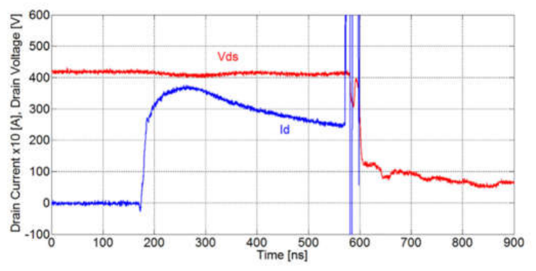
Figure 2.
Surface picture of the device failed under high-voltage short-circuit stress with different magnifications: (a) the picture of the chip, (b) a zoom of the failed region, (c) a further zoom of the failed region [20].
Figure 2.
Surface picture of the device failed under high-voltage short-circuit stress with different magnifications: (a) the picture of the chip, (b) a zoom of the failed region, (c) a further zoom of the failed region [20].
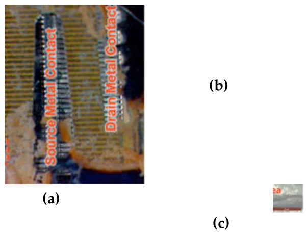
Figure 3.
Simulated lattice temperature within the structure at VDS = 360 V [19].
Figure 3.
Simulated lattice temperature within the structure at VDS = 360 V [19].
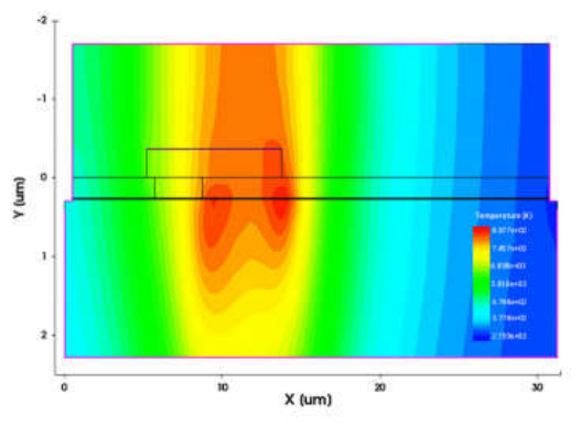
Figure 4.
Vds and Id waveforms measured in the SC test at VDS = 250 V and VGS = 5V, showing the low-voltage failure mode [20].
Figure 4.
Vds and Id waveforms measured in the SC test at VDS = 250 V and VGS = 5V, showing the low-voltage failure mode [20].
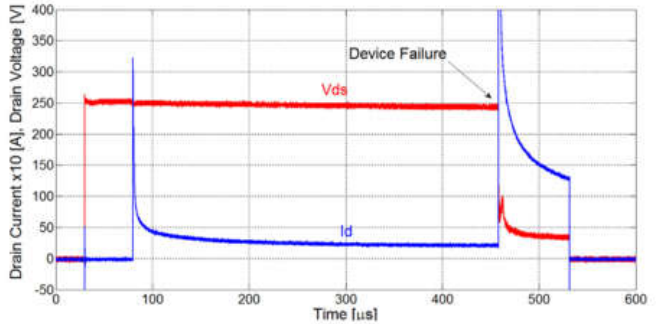
Figure 5.
Microscope picture of the failed device under low-voltage short-circuit stress: (a) overall chip view showing two distinct melting regions (A and B); (b) magnified view of the failed regions [20].
Figure 5.
Microscope picture of the failed device under low-voltage short-circuit stress: (a) overall chip view showing two distinct melting regions (A and B); (b) magnified view of the failed regions [20].
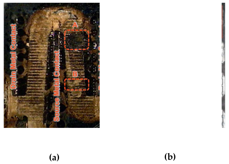
Figure 6.
Temperature distribution at tSC = 1 µs, VDS = 400 V, VGS = 6 V [27].
Figure 6.
Temperature distribution at tSC = 1 µs, VDS = 400 V, VGS = 6 V [27].
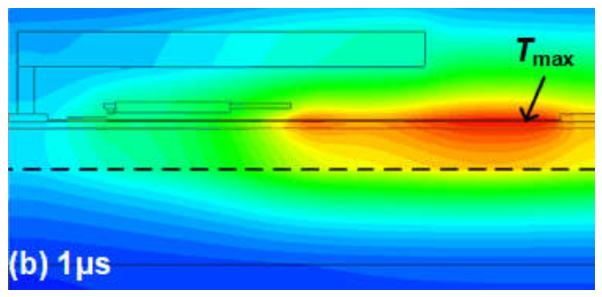
Figure 7.
Simulated thermomechanical stress distribution under short-circuit conditions [30].
Figure 7.
Simulated thermomechanical stress distribution under short-circuit conditions [30].
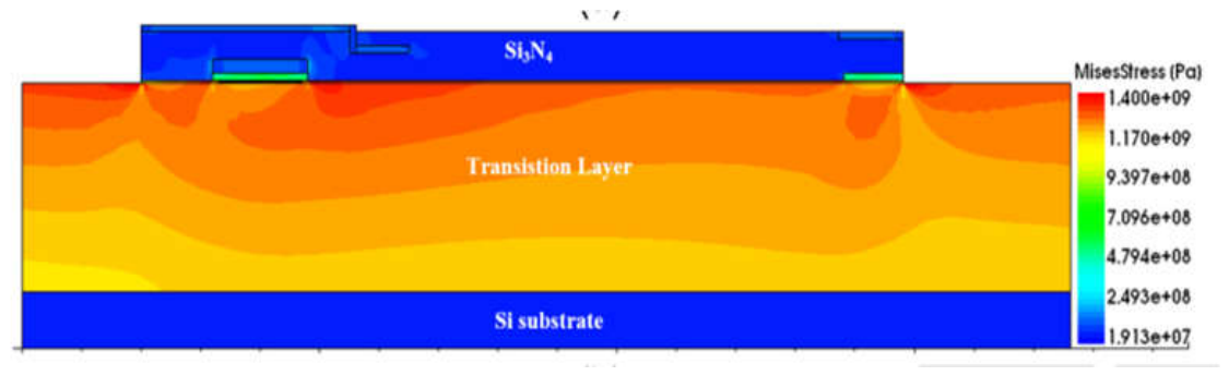
Figure 8.
(a) Cross-sectional view of a failed device after focused ion beam cutting (FIB). (b) Enlarged view of cracks at the GaN buffer layer–transition layer interface [28].
Figure 8.
(a) Cross-sectional view of a failed device after focused ion beam cutting (FIB). (b) Enlarged view of cracks at the GaN buffer layer–transition layer interface [28].
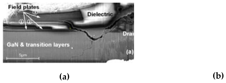
Figure 9.
(a) SC test circuit diagram of ITC57250. (b) Timing diagrams of SC gate/drain stress voltage [35].
Figure 9.
(a) SC test circuit diagram of ITC57250. (b) Timing diagrams of SC gate/drain stress voltage [35].
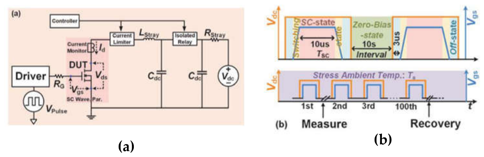
Figure 10.
(a) Positively shifted Vth versus SC cycles and (b) Ratio of on-resistance of DUT-1, DUT-2, and DUT-3. Stress condition: VGS = 6, 5, 4 V and VDS = 60 V. (c)Varied Vth versus SC cycles (d) Ratio of on-resistance of DUT-4, DUT-5, DUT-6, and, DUT-7. Stress condition: VGS = 5 V and VDS = 70, 60, 50, 40 V [35].
Figure 10.
(a) Positively shifted Vth versus SC cycles and (b) Ratio of on-resistance of DUT-1, DUT-2, and DUT-3. Stress condition: VGS = 6, 5, 4 V and VDS = 60 V. (c)Varied Vth versus SC cycles (d) Ratio of on-resistance of DUT-4, DUT-5, DUT-6, and, DUT-7. Stress condition: VGS = 5 V and VDS = 70, 60, 50, 40 V [35].
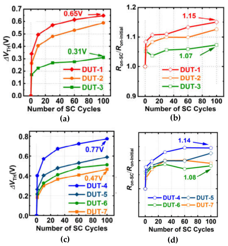
Figure 11.
(a) Variations in Vth and (b) variations in Ron after the first and tenth SC event under SC stress with VGS = 6 V and varied VDS. (c) Variations in Vth and (d) variations in Ron after the first and tenth SC event under SC stress with VGS = 6 V and varied VDS [31].
Figure 11.
(a) Variations in Vth and (b) variations in Ron after the first and tenth SC event under SC stress with VGS = 6 V and varied VDS. (c) Variations in Vth and (d) variations in Ron after the first and tenth SC event under SC stress with VGS = 6 V and varied VDS [31].
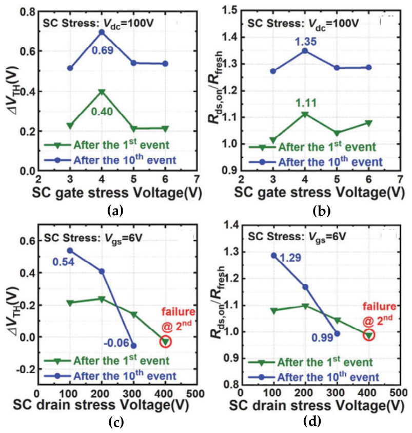
Figure 12.
(a) Energy-band diagram of the gate stack under low-voltage SC stress with VGS = 4 V, VDS = 100 V; (b) charge distribution and trap filling in the p-GaN gate HEMT [31].
Figure 12.
(a) Energy-band diagram of the gate stack under low-voltage SC stress with VGS = 4 V, VDS = 100 V; (b) charge distribution and trap filling in the p-GaN gate HEMT [31].
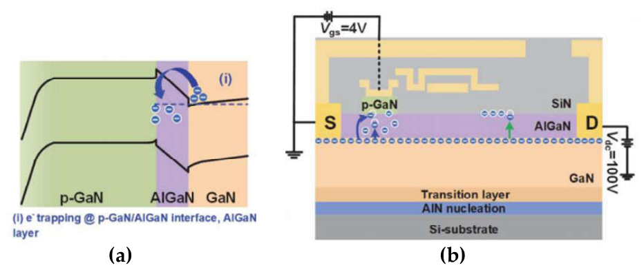
Figure 13.
(a)valence-band energy diagram in gate-stack under VGS = 6 V/VDS = 300 V, hole carrier distribution with stress of VGS = 6 V, (b) at VDS = 100 V; (c) at VDS = 300 V [31].
Figure 13.
(a)valence-band energy diagram in gate-stack under VGS = 6 V/VDS = 300 V, hole carrier distribution with stress of VGS = 6 V, (b) at VDS = 100 V; (c) at VDS = 300 V [31].
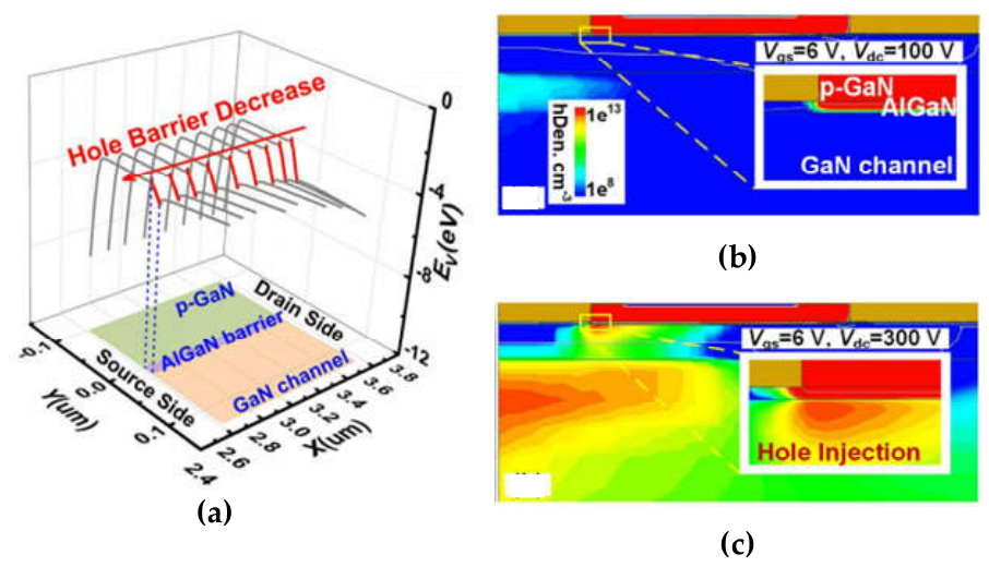
Figure 14.
(a) Energy-band diagram of the gate-stack region; (b) charge distribution and trap filling in the p-GaN gate HEMT under high-voltage SC stress (VGS = 6 V, VDS = 300 V) [31].
Figure 14.
(a) Energy-band diagram of the gate-stack region; (b) charge distribution and trap filling in the p-GaN gate HEMT under high-voltage SC stress (VGS = 6 V, VDS = 300 V) [31].
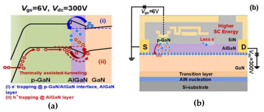
Figure 15.
Schematic structures of (a) the conventional p-GaN gate HEMT and (b) the proposed p-GaN gate HEMT with the SSE and (c) equivalent circuit of the p-GaN gate HEMT with the SSE [38,39].
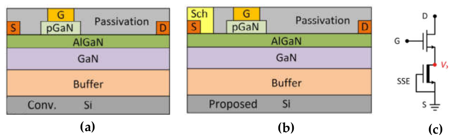
Figure 16.
Experimentally measured I-V characteristics of (a) a conventional p-GaN gate HEMT and (b) a proposed p-GaN gate HEMT with SSE [38].
Figure 16.
Experimentally measured I-V characteristics of (a) a conventional p-GaN gate HEMT and (b) a proposed p-GaN gate HEMT with SSE [38].
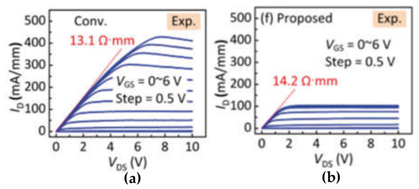
Figure 17.
Schottky source extension GaN HEMT: (a) pulsed ID–VDS characteristics of the conventional and proposed devices; (b) IOFF of the proposed device with SSE after each VDS, SC stress; and multi-pulse short-circuit test waveforms of (c) the conventional device and (d) the proposed device [38,40].
Figure 17.
Schottky source extension GaN HEMT: (a) pulsed ID–VDS characteristics of the conventional and proposed devices; (b) IOFF of the proposed device with SSE after each VDS, SC stress; and multi-pulse short-circuit test waveforms of (c) the conventional device and (d) the proposed device [38,40].
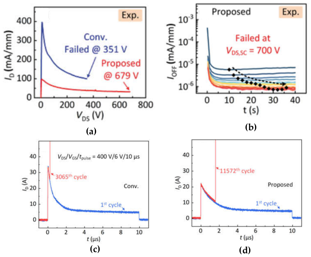
Figure 18.
Schematics of the dual-gate E-mode GaN HEMT (a) in the off-state (VG < Vth) and (b) in the on-state (VG > Vth) [41].
Figure 18.
Schematics of the dual-gate E-mode GaN HEMT (a) in the off-state (VG < Vth) and (b) in the on-state (VG > Vth) [41].
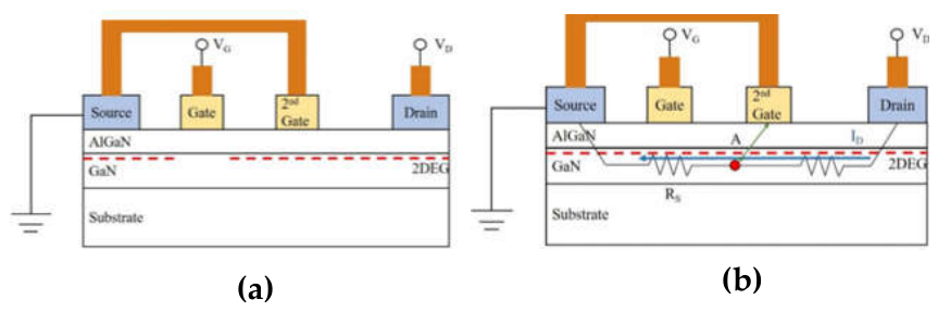
Figure 19.
Measured output characteristics of (a) single-gate HEMT and device with the MIS second gate. (b) single-gate HEMT and device with the Schottky second gate [41].
Figure 19.
Measured output characteristics of (a) single-gate HEMT and device with the MIS second gate. (b) single-gate HEMT and device with the Schottky second gate [41].
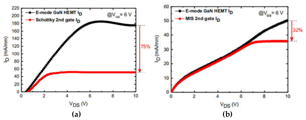
Figure 20.
Cross-sectional schematics of p-GaN gate AlGaN/GaN HEMTs: (a) the conventional p-GaN gate AlGaN/GaN HEMT and (b) the proposed p-GaN extended-gate AlGaN/GaN HEMT [42].
Figure 20.
Cross-sectional schematics of p-GaN gate AlGaN/GaN HEMTs: (a) the conventional p-GaN gate AlGaN/GaN HEMT and (b) the proposed p-GaN extended-gate AlGaN/GaN HEMT [42].
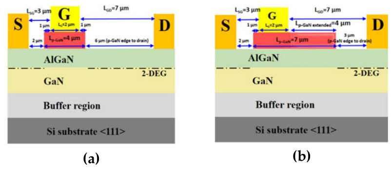
Figure 21.
Measured output characteristics of conventional HEMT and p-GaN extended gate HEMT [42].
Figure 21.
Measured output characteristics of conventional HEMT and p-GaN extended gate HEMT [42].
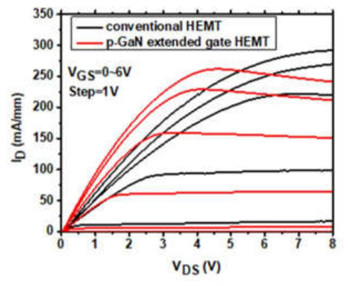
Figure 22.
The proposed p-GaN voltage seatbelt. Inset: equivalent operating configuration of the proposed structure [44].
Figure 22.
The proposed p-GaN voltage seatbelt. Inset: equivalent operating configuration of the proposed structure [44].
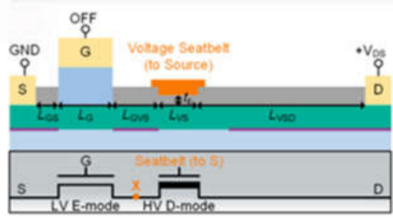
Figure 23.
Measured output characteristics of conventional device and proposed device [43].
Figure 23.
Measured output characteristics of conventional device and proposed device [43].
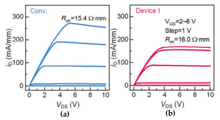
Figure 24.
(a) Pulsed short-circuit measurement waveforms. (b) Pulsed short-circuit measurement results of the conventional and proposed devices [43].
Figure 24.
(a) Pulsed short-circuit measurement waveforms. (b) Pulsed short-circuit measurement results of the conventional and proposed devices [43].
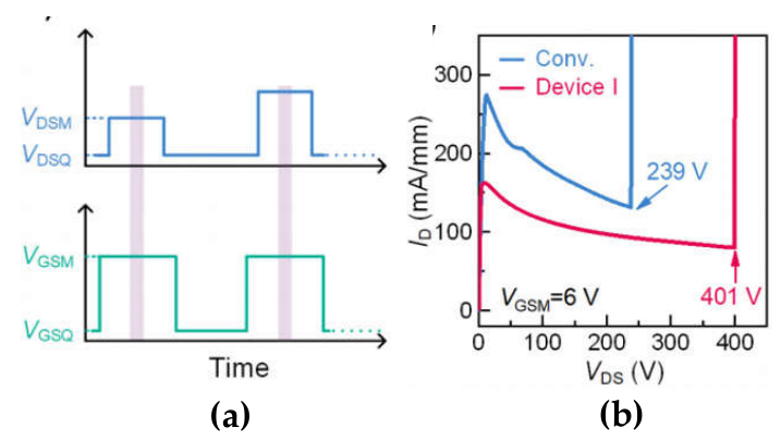
Figure 25.
output characteristics of three devices. DUT-A and DUT-B are conventional devices [44].
Figure 25.
output characteristics of three devices. DUT-A and DUT-B are conventional devices [44].
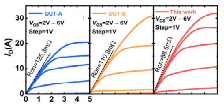
Figure 26.
(a) Measured waveforms of repetitive SC stress at VDS = 450 V, VGS = 6 V, and tSC = 10 µs. (b) Normalized composition of ΔIds for DUTs at t1–t3[44].
Figure 26.
(a) Measured waveforms of repetitive SC stress at VDS = 450 V, VGS = 6 V, and tSC = 10 µs. (b) Normalized composition of ΔIds for DUTs at t1–t3[44].
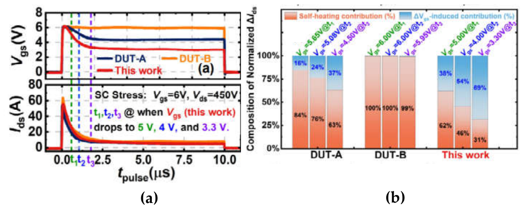
Figure 27.
Measured waveforms: single-pulse short-circuit waveform of (a) VGS and (b)Ids at VDS = 450 V and VGS = 6 V; (b) repetitive short-circuit waveforms at VDS = 450 V and VGS = 6 V with a 5s interval between consecutive short-circuit pulses, tSC = 10 μs; (c) tSC = 50 μs [44].
Figure 27.
Measured waveforms: single-pulse short-circuit waveform of (a) VGS and (b)Ids at VDS = 450 V and VGS = 6 V; (b) repetitive short-circuit waveforms at VDS = 450 V and VGS = 6 V with a 5s interval between consecutive short-circuit pulses, tSC = 10 μs; (c) tSC = 50 μs [44].
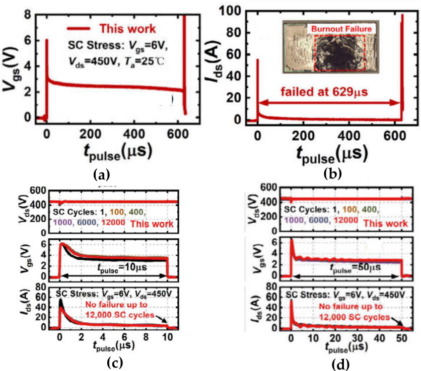
Figure 28.
(a) Benchmark of single-pulse SC. (b) Benchmark of repetitive SC capability [44].
Figure 28.
(a) Benchmark of single-pulse SC. (b) Benchmark of repetitive SC capability [44].
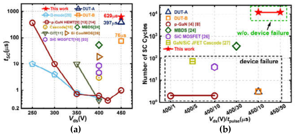

Table 1.
Summary of repetitive and single-event short-circuit withstand capabilities of representative GaN HEMTs under various bias conditions.
Table 1.
Summary of repetitive and single-event short-circuit withstand capabilities of representative GaN HEMTs under various bias conditions.
| Rated voltage(V) | VGS(V) | VDS(V) | SCWT(μs) | Number cycle(Nc) | tsc(μs) |
| 650 | 0 | 400 | <1[18] | NA | NA |
| 650 | 6 | 420 | 0.57[20] | NA | NA |
| 650 | 6 | 350 | <1[34] | NA | NA |
| 650 | 5 | 350 | ~0.7[23] | NA | NA |
| 650 | 6 | 400 | NA | 2 | 1[27] |
| 650 | 6 | 400 | NA | 2 | 10[31] |
Disclaimer/Publisher’s Note: The statements, opinions and data contained in all publications are solely those of the individual author(s) and contributor(s) and not of MDPI and/or the editor(s). MDPI and/or the editor(s) disclaim responsibility for any injury to people or property resulting from any ideas, methods, instructions or products referred to in the content. |
© 2026 by the authors. Licensee MDPI, Basel, Switzerland. This article is an open access article distributed under the terms and conditions of the Creative Commons Attribution (CC BY) license.
Copyright: This open access article is published under a Creative Commons CC BY 4.0 license, which permit the free download, distribution, and reuse, provided that the author and preprint are cited in any reuse.