

Submitted:
03 September 2026
Posted:
07 September 2026
You are already at the latest version
Abstract
Commercial power electronics laboratory platforms remain either prohibitively expensive or limited to a single converter topology, restricting student exposure to modern digital control challenges. This paper presents a versatile, low-cost didactic platform built from off-the-shelf components, the Infineon XMC4700 microcontroller and the STMicroelectronics X-NUCLEO-IHM07M1 motor-driver expansion board, engineered to support multiple power-electronics experiments without hardware reconfiguration. The platform exploits the L6230 three-phase DMOS driver as a reconfigurable set of three independent half-bridges, enabling closed-loop DC/DC conversion, brushed DC motor speed control, and three-phase inverter operation on a single physical setup. The software workflow combines the XMC4700's DAVE™ Integrated Development Environment (IDE) with PLECS simulation and C-script code block, allowing students to validate control strategies in simulation before porting them to hardware with minimal adaptation. Real-time supervisory control is provided through Micrium μC/Probe XMC, eliminating the recompile–reflash cycle during tuning. Each of the three case studies is documented with complete schematics, control diagrams, and experimental waveforms. The platform is approximately one-tenth the cost of equivalent commercial benches, requires no paid software or licenses, and has been validated in two different Power Electronics courses.
Keywords:
DC‐AC power converters
; DC‐DC power converters
; educational technology
; microcontrollers
; power electronics
; power engineering education
1. Introduction
The field of power electronics is foundational to modern electrical engineering, serving as the critical interface between energy generation and consumption. As global energy systems transition toward electrification, renewable integration and electric mobility, the demand for engineers proficient in the design and control of power converters has reached unprecedented levels. Unlike purely theoretical disciplines, power electronics is inherently multidisciplinary and demands mastery of circuit analysis, analog and digital electronics, sensors and signal conditioning, digital control theory and hardware implementation, which makes hands-on laboratory experience indispensable.
Two co-existing limitations, however, constrain the availability of such laboratory infrastructure: prohibitive cost and architectural inflexibility. Commercial industrial-style workbenches provide a robust environment for high-power experimentation, but require substantial capital investment and ongoing maintenance, which restricts their deployment to a small number of well-funded institutions (Ulrich, 2017). Equally limiting, these systems are typically closed, "black-box" configurations with fixed topologies that prevent students from exploring modern, reconfigurable converter architectures or implementing contemporary digital-control strategies.
To mitigate these limitations, modular didactic kits have been proposed. Platforms built on off-the-shelf microcontrollers and discrete power stages, such as the versatile low-cost DC/DC system in (Ulrich, 2017) and the educational buck converter in (Matoso et al., 2025), enable direct engagement with hardware-level component selection. Nevertheless, modular kits typically realize a single converter topology, and scaling them to a large cohort quickly becomes cost-prohibitive. The workshop-based approach in (Corti, et al., 2024) is constrained to a fundamental buck converter, while the off-the-shelf platform in (Santos et al., 2025) extends coverage to a bidirectional boost converter, three-phase inverter and permanent-magnet synchronous motor but relies on the Texas Instruments C2000 ecosystem, which still presents a steep learning curve for students unfamiliar with its hardware-abstraction layer and offers only limited support for graphical real-time tuning of control parameters. The reconfigurable platform proposed by (Mahmoudi et al., 2018) is not sufficiently portable to be carried outside the classroom and developed independently by each student group, since its multi-board benchtop arrangement demands a fixed laboratory installation. Furthermore, even though the authors describe the hardware as open-source and easily replicable, the proposed 653 USD per-unit cost combined with dependence on commercial, non-free software tools makes the replication of one kit per project group hard to justify economically. The didactic platform proposed by (Franca et al., 2022) is constrained to a 450 V DC-link, a level that restricts its routine use in standard undergraduate laboratories. The absence of integrated current sensing leaves closed-loop experiments beyond the platform's validated scope.
The shift from analog to digital control, driven by the demand for complex algorithms such as space vector modulation, model-predictive control and sensorless field-oriented control, has made digital control development no longer optional. Modern engineers are expected to manage hard real-time constraints, synchronize analog-to-digital conversion with PWM generation, and exploit the computational bandwidth of microcontrollers or DSPs. Yet the multidisciplinary nature of this task routinely overwhelms the time allocated to a standard semester: students get caught up in bitwise programming and register-map configuration, which distracts them from the primary control objectives and erodes the time available for design iteration. Hardware-in-the-loop teaching platforms partially decouple control design from physical hardware by emulating the power stage in real time, which enables safe experimentation with extreme operating conditions and reduces the cost of repeated prototyping. However, this approach is typically implemented on field-programmable gate arrays (Lamo et al., 2020) and reintroduces the very complexity it is meant to offset (FPGA synthesis, hardware-description-language coding, and the manual derivation of piecewise-linear state equations) while removing the tactile engagement with a real converter that is essential for developing hardware intuition. A fast learning curve in embedded programming, complemented by graphical real-time tuning of control parameters, is therefore not a luxury but a prerequisite for closed-loop operation.
There remains a clear need for a didactic solution that combines industrial-grade hardware flexibility with a streamlined digital-control development workflow, supports multiple converter topologies on a single reconfigurable board, and brings students as close as possible to real hardware while keeping the programming burden manageable.
This paper addresses these challenges by presenting a versatile and low-cost didactic platform that integrates the Infineon XMC4700 microcontroller with the STMicroelectronics X-NUCLEO-IHM07M1 expansion board. This combination establishes a reconfigurable architecture where a single physical set of hardware can accommodate diverse educational case studies. The X-NUCLEO-IHM07M1, based on the L6230 DMOS driver, provides three independent half-bridges and integrated sensors, making it suitable for both DC-DC and DC-AC applications. Moreover, the low cost of the platform makes it feasible for each student to be provided with an individual kit, enabling project development outside the laboratory and allowing students to manage their own working time. On the software side, this work streamlines the student development workflow through several integrated layers:
- DAVE™ Apps: Programming on the XMC4700 is accelerated using these high-level graphical design entities, which provide configurable functions that eliminate the need for mastering low-level register maps;
- PLECS Integration: The workflow leverages PLECS for piecewise linear simulation and C-script code development and validation. This allows students to focus on high-level control strategies and ensures that the transition from simulation to hardware is seamless;
- Micrium μC/Probe XMC: Real-time supervisory control is facilitated via this graphical interface, acting as a "virtual dashboard" for monitoring variables and tuning control parameters without stopping the processor.
The multifunctionality of the proposed platform is validated through three distinct case studies: (i) the closed-loop control of a synchronous boost converter, ii) closed-loop speed control of a brushed DC motor and (iii) the open-loop control of a three-phase inverter. Note that by using these case studies the flexibility of the X-NUCLEO-IHM07M1 is demonstrated since it is used one, two and three half-bridges, respectively.
The proposed power and control platform is developed on a fully integrated and modular framework that leverages the specialized capabilities of the X-NUCLEO-IHM07M1 power expansion board and the high-performance Infineon XMC4700 microcontroller, natively simulated and validated within the PLECS environment. This approach eliminates the complexities of manual, low-level register configuration by utilizing graphical DAVE™ Apps for PWM, Space Vector Modulation (SVM), ADC, and interrupt handling on the XMC4700, while ensuring real-time monitoring and parameter tuning through the Micrium μC/Probe XMC supervisory interface.
Finally, regarding economic aspects, only a few of the previously discussed approaches present a cost analysis of their platforms. The didactic platform for flexible power electronic converters proposed in (Franca et al., 2022) reports a cost of 136.36 USD per unit (excluding the DSP), while the reconfigurable rapid prototyping platform described in (Mahmoudi et al., 2018) amounts to 653 USD. In contrast, the platform proposed in this work is assembled from low-cost commercial off-the-shelf components: the X-NUCLEO-IHM07M1 power board costs (as June 2026) 13.5 USD and the Infineon XMC4700 Relax Lite Kit microcontroller costs 19.4 USD, to which an estimative of 3.7 USD for external passive components is added depending on the specific converter under study. If the load is a DC motor with an encoder, it adds an additional cost of 13.4 USD. The resulting overall cost of approximately 50 USD per unit represents, to the best of the authors' knowledge, the lowest value published in the literature for a power electronics didactic platform.
The remainder of this paper is structured as follows: Section II characterizes the experimental platform, namely the X-NUCLEO-IHM07M1 power board, the XMC4700 microcontroller and the PLECS simulation software. Section III describes the digital modulator and sampling architecture, including the continuous-time PI controller for the inner current loop, its discretization by the Tustin approximation, the sampling architecture on the XMC4700, and the empirical PI tuning procedure. Section IV presents three case studies: the closed-loop control of a boost converter, the closed-loop control of a DC motor, and the open-loop control of a three-phase inverter. Section V details the methodology employed, and Section VI concludes the paper.
2. Platform Characterization
2.1. X-NUCLEO-IHM07M1 Power Board
2.1.1. X-NUCLEO-IHM07M1 Technical Overview
The X-NUCLEO-IHM07M1 (Figure 1) is a low-voltage, highly flexible three-phase brushless DC (BLDC) and permanent magnet synchronous motor (PMSM) driver expansion board developed by STMicroelectronics. It is designed to offer a modular, compact, and affordable solution (13.5 USD July 2026) for low-power motor control and power electronics development. The core of the board is the L6230 driver. The device integrates six isolated power MOSFETs configured as a three-phase inverter bridge alongside standard CMOS and bipolar control circuits on a single monolithic chip.
Figure 2 shows the power circuit diagram of the IHM07M1 module implemented in PLECS simulator, including the power terminals (Vin, GND, out1, out2, and out3), as well as the Enable terminals for each arm (Enable_CHx) and the PWM control terminals (xH_PW). To ensure the PWM signals are applied to the MOSFETs only when the Enable pin is set to logic level 1, the enable logic and complementary PWM signals were implemented using standard AND and NOT gates. Also shown are the voltage divider for measuring voltage on the input DC bus, the input filter capacitor, and the shunt resistors for measuring current in the arms. Other sensors included in the module (but not shown in the figure) are the three Hall effect sensors for controlling BLDC motors and the temperature sensor located next to the L6230 driver. The sensors operate with analog signals in the 0-3.3V range. In addition, the module also includes a potentiometer and an LED as add-ons for general use.
Key hardware specifications of the expansion board include:
- Operating supply voltage: The board accommodates a nominal power supply ranging from 8 VDC to 48 VDC;
- Output current capacity: It supports an output peak current of up to 2.8 A (with a continuous capability of 1.4 A RMS), featuring non-dissipative overcurrent protection on the high-side transistors;
- Switching frequency: The bridge is capable of highly efficient operational frequencies up to 100 kHz, allowing for high performance SVM or high frequency PWM regimes;
- Integrated protections: Cross-conduction prevention is implemented by hardware internal logic providing a dead time (typically 1 µs) between upper and lower complementary switches. It also includes an embedded thermal shutdown circuit (tripping at 165° C) and an undervoltage lockout system.
This module, initially designed to drive BLDC or PMSM motors, is actually very flexible, allowing for different experiments with the addition of a few external components.
2.1.2. Interface Integration with Case Studies
The conceptual architecture establishes how a single physical piece of hardware can be hardware-reconfigured to accommodate vastly diverse educational and industrial case studies. The structural versatility of the L6230 Power Bridge enables its operation across distinct target setups without modifying the physical hardware, driven entirely through structural code blocks mapped from the Infineon XMC4700:
- Closed-Loop Control of a Boost Converter:
By utilizing a single-phase leg (e.g., Phase A/out1), an inductor is connected between the external DC input and the output terminal (out1). The high-side and low-side switches are driven with complementary PWM signals to function as a bidirectional synchronous boost stage, regulating the DC link voltage on the output capacitor bank.
- Speed Control of a Brushed DC Motor:
Two of the three available phase legs are configured to form a full H-bridge, supplying bidirectional voltage to a brushed DC machine, while the third phase leg remains disabled in a high-impedance state.
- Three-Phase Inverter Operation:
All three legs are operated concurrently using Sinusoidal Pulse Width Modulation (SPWM) or SVM to generate balanced three-phase AC currents across a symmetric star-connected resistive-inductive (RL) load.
2.1.3. Pin Mapping and XMC4700 Microcontroller Interconnection
To implement these multi-topology frameworks, the X-NUCLEO-IHM07M1 pins must be mapped onto the pin arrangement of the Infineon XMC4700 Relax Kit or custom development board. Table 1 maps the main operational pins of the X-NUCLEO-IHM07M1 expansion board to their corresponding signals and functions.
2.1.4. Closed-Loop Sensing Functionality
For precise closed-loop control algorithms such as Field Oriented Control (FOC) or current-mode DC/DC regulation, the X-NUCLEO-IHM07M1 provides an integrated independent current sensing scheme. The architecture inserts low-impedance power shunt resistors (0.33Ω / 1 W) between the source terminals of the three low-side MOSFET transistors and the power ground plane. The voltage drop developed across these shunts represents the raw phase currents. This raw analog signal undergoes immediate signal conditioning via an on-board TSV994IPT operational amplifier circuit (Figure 3). The TSV994 is a wide-bandwidth (20 MHz) rail-to-rail input/output quad operational amplifier optimized for precise analog routing. The gain stage is hardware-configurable via solder bridges and headers to operate in either a single-shunt mode or a three-shunt mode (for FOC implementations). In the standard three-shunt configuration used here, the differential op-amp circuit introduces an experimental overall voltage gain and an analog level shift to map the bidirectional alternating phase currents into the positive 0 V to 3.3 V range acceptable by the microcontroller's ADC. To recover the actual phase current in Amperes from the sampled digital representation, the microcontroller firmware must apply the inverse transformation function:
where vi_measured represents the analog voltage sampled at the ADC, and ireal yields the actual line current in Amperes flowing through the leg.
To protect the inverter bridge from overvoltage transients and to feed the voltage-loop controller in DC/DC topologies, an independent voltage sensing network is embedded on the expansion board (Figure 4). The measurement block reads the high-voltage DC bus line (VIN+/VBUS) directly through a resistor voltage divider network consisting of a high-side resistor R17 (169 kΩ, 1% tolerance) and a low-side ground-referenced resistor R18 (9.31 kΩ, 1% tolerance). The output of this divider is filtered against high-frequency switching noise by a parallel decoupling ceramic capacitor C14 (4.7 nF / 10 V), creating a low-pass filter corner frequency that dampens ringing without introducing prohibitive control loop lag. This conditioned signal is routed directly to the microcontroller's ADC input via pin 30 of header CN7. The inverse mapping function implemented inside the XMC4700 processing block to recover the real physical DC-bus voltage is expressed as:
where vmeasured (VBUS_SENS) is the raw voltage presented at the ADC pin, and vreal (VIN+) represents the recovered actual DC-link voltage in Volts.
2.2. Microcontroller
2.2.1. XMC4700 Microcontroller Architecture
The Infineon XMC4700 is a 32-bit microcontroller family based on the ARM Cortex-M4 processor core running at 144 MHz. Purpose-built for industrial applications, power electronics and motor control, the architecture merges standard execution efficiency with specialized hardware peripherals (Jhawar et al., 2024; Setka & Tolar, 2018; Yang et al., 2015) This tight integration ensures deterministic real-time processing and avoids the execution bottlenecks common in general-purpose microcontrollers. Central to the XMC4700's performance in power electronics is its modular peripheral matrix. Key features include a nested vector interrupt controller, a floating-point unit, up to 2 MB of high-speed embedded Flash memory, and 352 KB of SRAM. Rather than overloading the CPU core with computational tasks or continuous signal tracking, the XMC4700 relies on smart, autonomous co-peripherals. These components can be linked together using a programmable event routing matrix, optimizing the execution of closed-loop control tasks.
Programming development on the Infineon XMC4700 is streamlined and accelerated using high-level graphical design entities known as DAVE™ Apps (Figure 5) and their corresponding configurable functions, which eliminate the traditional necessity of mastering low-level register maps and complex bitwise parameters.
Instead of manually parsing extensive hardware reference manuals to calculate timer clock prescalers, configure multi-channel interrupt vector registers, or construct nested bit masks for parallel analog sampling, developers interact with intuitive graphical interfaces. Within these DAVE™ Apps, critical hardware behaviors, such as the exact dead-time insertion for a complementary PWM block, the structural conversion triggers for an ADC channel, or the edge-detection logic for an external hardware interrupt, are handled via dropdown menus, numerical entry fields, and automated validation rules (Figure 6). The tool's underlying engine automatically parses these visual configurations, resolves internal resource allocations, and generates optimized, fully documented ANSI-C APIs that manage the low-level register abstractions seamlessly behind the scenes.
In power converter topologies, the generation of high-frequency, synchronized PWM signals is paramount. The XMC4700 implements this via the Capture and Compare Units, CCU4 and CCU8 peripheral Apps. In CCU8, each slice features a pair of compare channels capable of driving complementary outputs with software-managed dead-time insertion.
The DAVE™ IDE simplifies implementing complex modulation strategies like SVM or complementary synchronous switching. Instead of writing low-level bit masks to register blocks, developers select and use a visual graphical user interface. This interface directly maps dead times, asymmetric duty cycles, and output passive states. Crucially, the module operates independently of the CPU core after initialization. The timers run continuously based on internal shadow registers, which update values safely at the timer's period match or underflow points. This hardware-shadowed update system avoids glitching or asymmetric duty cycle distortion mid-period, ensuring safe operation of high-power MOSFET bridges. A major challenge in digital power electronics control is capturing accurate analog signals, such as inductor current or bus voltage, without introducing phase lag or capturing switching noise. The XMC4700 features a modular, multi-group Versatile Analog-to-Digital Converter (VADC) subsystem. The VADC contains up to 4 independent analog-to-digital converter kernels, enabling simultaneous parallel sampling across multiple channels with resolution up to 12 bits and conversion times under 1 microsecond. The architecture simplifies signal acquisition through an integrated hardware interconnection link that ties the CCU8 timer slices directly to the VADC conversion trigger lanes.
2.2.2. Real-Time Supervisory Control via Micrium μC/Probe XMC
During the validation and optimization phases of power converters, developers often need to change system variables or tune control parameters, such as the proportional and integral gains of a PI controller and observe system responses in real time. Traditionally, this required stopping the controller, modifying variables in software, recompiling, and reflashing the firmware. The Micrium μC/Probe XMC software tool addresses this limitation by acting as a real-time graphical user interface (GUI) and supervisor for XMC microcontrollers. Figure 7 presents an example of a GUI developed in Micrium μC/Probe XMC.
The Micrium μC/Probe XMC architecture operates by reading global variable addresses directly from the compilation output file (the target.elf). The tool uses standard debugging interfaces, such as Segger J-Link to read and write data directly to the microcontroller's RAM memory map during runtime. The user interface features a drag-and-drop workspace where developers can quickly link graphical dashboard elements directly to active firmware variables. For example, linear sliders or numeric entry fields can be mapped to variables like the reference boost voltage or the PI controller tuning parameters. When a user modifies a slider on the dashboard, μC/Probe safely updates the underlying value in RAM over the JTAG link, allowing for real-time parameter tuning.
2.3. PLECS Simulation Software
PLECS is a high-performance simulation software package developed by Plexim. Specifically engineered for power electronic systems, PLECS circumvents the computational bottlenecks typical of general-purpose circuit simulators (such as standard SPICE engines) by modeling electrical components as piecewise linear elements. This approach allows for rapid, robust, and highly deterministic simulation times, making it an industry and academic standard for developing complex topologies, motor drives, and grid-tied converter systems. PLECS features a comprehensive library of multi-domain components together with an advanced control system library. This enables the complete interaction between electrical circuits and other physical subsystems such as thermal modeling, magnetic domain and mechanical domain.
With the PLECS Coder, the software can translate schematics automatically into high-quality, real-time ANSI-C code. This code can be deployed onto real-time targets, such as PLECS RT Box, or third-party microcontrollers for Hardware-in-the-Loop (HIL) testing and rapid control prototyping. One of the most powerful and heavily utilized features of PLECS, particularly for embedded systems developers and control engineers, is the C-script block. When designing modern power electronics, control strategies are almost exclusively implemented digitally using microcontrollers or FPGA. The C-script block allows users to type standard ANSI-C code directly into the simulation environment. This means that code verified and developed within the simulation environment (such as an inner current PI control loop or an outer voltage loop) can be copy-pasted directly onto the target microcontroller with minimal syntax adaptation. Power electronics rely heavily on precise sampling. The C-script block can be explicitly configured to run as a discrete-time subsystem. Users define a sample period (e.g., matching a given switching frequency or interrupt service routine). PLECS ensures that the C-code executes at exactly those discrete time step boundaries, capturing realistic digital behaviors like quantization, computational delays, and execution latencies. This capability facilitates a seamless transition from the simulation model to the physical DSP/microcontroller implementation, significantly reducing the gap between prototyping and final deployment (Santos et al., 2025).
Figure 8 presents an example of closed-loop control implementation with C-Script in the PLECS environment, illustrating the seamless integration of discrete-time controllers with the power stage. The example represents a typical DC-DC converter voltage control loop with the reference voltage (15 V), the sensed output voltage (Vo), and the calculated duty cycle value that produces the PWM signal at 10 kHz.
So, the C-Script block receives the voltage error as an input and deliveries the calculated duty-cycle as an output. Inside the C-Script block it is possible to configure the desired number of inputs/outputs, the sampling period (typically equal to the inverse of the PWM switching frequency) among other parameters. The main code block is structured in the “Code” tab into code declarations, start, output, and update functions that define the control logic, ensuring deterministic execution at the specified sample rate. Figure 9 illustrates the “Code declarations” section example of the discrete PI controller, and it can be seen the constants and variables initialization, and the discrete PI code inside the “interrupt” function that is called trough the output section at the defined sampling rate.
By combining the speed of ideal piecewise linear circuits with the native execution of discrete C-coded algorithms, PLECS provides an optimal simulation ecosystem for verifying embedded control code under realistic circuit conditions before hardware validation.
3. Digital Modulator and Sampling Architecture
This section establishes the digital control layer that the case studies of Section IV re-use without re-deriving. The material is organized in the four laboratory steps that a student implements on the XMC4700 Relax Kit:
- (i)
- Formulation of a continuous-time PI controller (for instance, the inner peak current-mode loop of a DC/DC stage);
- (ii)
- Selection of the discretization rule and derivation of the equivalent discrete-time transfer function in the Z-domain;
- (iii)
- Definition of the ADC sampling instants relative to the timer events on the CCU8 slice and the VADC request line;
- (iv)
- Deployment of the resulting difference equation on the microcontroller.
Implementation details in XMC4700 firmware through the DAVE™ Apps were already introduced in Section II.2, followed by empirical refinement of the gains through the Micrium μC/Probe XMC. The architectural primitives called upon in what follows are the same blocks already characterized in Section II.2, and the simulation counterpart of the discrete-time controller is implemented through the PLECS C-Script block described in Section II.3. For didactic clarity, only the peak current-mode current loop of a DC/DC converter is analyzed throughout the following section.
3.1. Continuous-Time PI Controller for the Current Loop
Figure 10 reproduces the generic closed-loop architecture of a power converter that serves as the reference diagram for the rest of the section. The reference current is compared with the measured current to produce the error that drives the controller. The controller output takes the form of a duty-cycle level , which is then translated into the PWM signal applied to the converter power stage. Disturbances acting on the plant close the loop together with the output sensor. A complete two-loop implementation of a DC/DC stage uses an outer voltage loop that generates the current reference for a faster inner current loop that regulates the inductor current on a cycle-by-cycle basis. In the laboratory framing adopted here, only the inner loop is treated analytically, namely the peak current-mode current loop that regulates, for instance, the inductor current in a boost converter.
The classical feedback compensator belongs to the PID family. Two equivalent parameterizations are commonly used. In the parallel form the controller in the continuous-time domain is:
which in the Laplace domain becomes:
with , and the proportional, integral and derivative gains, respectively. In the standard form the same controller is expressed through the proportional gain and the integral and derivative time constants and , yielding:
in the Laplace domain, and:
in the continuous-time domain.
The derivative term is rarely used in power-converter control because it amplifies the high frequency switching noise that is inevitably present in the sensed waveforms (Kapat & Krein, 2011; Petrić et al., 2021; Xin et al., 2015) and because it complicates the anti-windup logic that is mandatory when a saturation limit is enforced on the duty cycle. The controller reduces accordingly to a proportional-integral regulator:
with . The PI form is therefore the canonical starting point for the digital control design of the boost current loop in this section. The same approach can be used for the case studies presented in Section IV, namely for the DC-motor armature loop and of the line-current loop of the three-phase inverter.
3.2. Discretisation of the PI Controller
The continuous-time controller cannot be evaluated directly by the XMC4700 firmware: at every sampling tick the controller can only act on a finite set of numerical inputs, and its output must reduce to a single deterministic update of the timer's compare register. A discrete-time counterpart must therefore be derived before the firmware loop can be written. Several discretisation rules are available to that end (forward Euler, backward Euler, zero-order hold, matched pole-zero and the bilinear transform). Of these, the Tustin approximation, also called the bilinear transform or trapezoidal approximation, is the standard choice in power converter digital control because it preserves the stability and the minimum-phase property of any continuous-time controller whose discretised form is derived by it (Jiang et al., 2024). Its defining relation is:
where is the sampling period. Substituting (8) into (7) we have:
and expressing the result for u(z), where denotes the unit-delay operator:
Writing for the sampled current error at sampling tick , for the duty-cycle command placed in the timer compare register, Eq. 10 translates into the linear difference equation:
Eq. 11 is precisely the algorithmic backbone of the firmware implementation executed once per sampling tick; in C syntax, the same update reads:
and the new value of the duty cycle (pi_out) is written to the CCU8 compare register before the next period-match event. A final note regarding anti-windup, which is mandatory whenever the discrete integrator is incremented past a saturation that the firmware enforces on ; otherwise, the integral component accumulates during the saturation interval and produces a large overshoot when the controller re-enters its linear regime.
3.3. Sampling Architecture on the XMC4700
Section III.A and III.B have produced a closed-form discrete-time controller that can be evaluated numerically once per sampling tick. The sampling tick itself has not yet been linked to the switching period; this is the role of the sampling architecture introduced in this subsection, and which is built directly on the CCU4/CCU8 and VADC peripherals already characterized in Section II.2.
The inner current loop is updated at the switching frequency, so the sampling frequency is set equal to the converter switching frequency, . Under this assumption the ADC is triggered once per PWM period, and the design of the digital controller reduces to the analogue-equivalent analysis of Section III.A sampled at . The same convention is adopted throughout the case studies of Section IV. The outer voltage loop of a two-loop controller must be updated at a slower rate, typically at for a discrete-time separation of one decade between the two loops.
The choice of the sampling instant within the PWM period depends on the control type to be implemented. For peak current-mode boost implementation, the inductor current must be sampled at the falling edge of the PWM signal. The ADC must be triggered at this instant, that corresponds to the “Period match” event of this signal. This architecture is summarized in the timing diagram of Figure 11, which shows the PWM carrier signal, the discretized duty-cycle signal, the compare event generating the PWM edges, the resulting PWM waveform, the period-match instant that fires the ADC sampling and the converter’s current variation.
The trigger is delivered through a dedicated request line from the timer to the ADC. On the XMC4700 platform this line is the CCU8-to-VADC internal request line already described in Section II.2, which enables the timer slice and the converter group to be synchronized without CPU intervention and thereby guarantees a deterministic sample rate across switching cycles. After the ADC conversion completes, the measured value is stored in the ADC result register and the converter can raise an end-of-conversion interrupt whose service routine copies the value into a memory location accessible to the PI computation.
The configuration (Figure 12) of the sampling chain is performed graphically inside DAVE™. Three steps are required:
- (1)
- In the PWM_CCU8 App, the Period Match event is enabled in the Timer Event Settings panel and is exposed as a hardware signal connection whose target signal is the trigger_input of the ADC_MEASUREMENT_0 App;
- (2)
- In the ADC_MEASUREMENT_0 App, the General Settings are set to External Trigger Upon Rising Edge, so that the rising edge of the period-match pulse initiates the conversion, and the end-of-conversion interrupt is enabled in the Interrupt Settings panel, with a function (interrupt handler name) that will be invoked from main.c;
- (3)
- The interrupt function, created before main, is the place where the PI update is executed, using the ADC_MEASUREMENT_GetResult function to read a 12-bit value in the range 0–4095, which corresponds to the 0–3.3 V full-scale input range of the VADC.
The interface between the firmware and the physical power stage is fixed by the L6230 driver on the X-NUCLEO-IHM07M1 board. The driver exposes three independent half-bridges whose high-side PWM inputs are mapped to the XMC4700 pins as documented in Table 1 of Section 2.1, and whose low-side current-sense outputs (one per phase leg, plus the DC-bus voltage sense) are routed to the VADC inputs already used by the current and voltage sensing networks of Figure 3 and Figure 4 in Section II.1. Selectivity between the case studies of Section IV is obtained entirely through firmware by enabling or disabling the Enable_CHx pins and the corresponding PWM legs on the XMC4700: a single leg is enabled for the boost case study, two legs are configured as a full H-bridge for the DC-motor case study, and three legs are operated concurrently for the three-phase inverter case study. Because of this firmware-driven approach, the sampling architecture and the Tustin-based difference equation are reused unchanged across all three case studies.
3.4. Empirical PI Tuning
While the analytical formulation can provide a theoretical starting point for control parameters, real world non-idealities, such as sensor noise and parasitic elements in the power stage, often necessitate manual refinement of the proportional and integral gains. Consequently, the tuning procedure usually involves a systematic experimental trial-and-error process, where the gains are adjusted to mitigate steady-state error while maintaining a transient response with acceptable overshoot and settling time. On the laboratory platform two complementary refinements are available: a Ziegler–Nichols-style empirical procedure executed on the plant, and a real time tuning interface that adjusts the gains of a running controller.
The proposed empirical procedure is a variation of the Ziegler–Nichols Continuous Cycling Method and it can be characterized by the following four steps:
- (1)
-
Step 1: Disable integral action and initial proportional gain
- (a)
- Set KI to zero (or a very low value).
- (b)
- Set KP to a small, non-zero value.
- (c)
- Ensure the converter is operating close to the desired steady-state point.
- (2)
-
Step 2: Find the Ultimate Gain Kcu
- (a)
- Slowly increase KP while observing the output voltage.
- (b)
- Increase KP until it is observed a sustained, constant-amplitude oscillations in the output voltage. This is the point of critical stability.
- (c)
- The value of KP at which these sustained oscillations occur is the Ultimate Gain Kcu.
- (d)
- Measure the period of these sustained oscillations in seconds, which is the Ultimate Period Tu.
- (3)
- Step 3: Calculate PI controller parameters
After definition of Kcu and Tu, use the classic Ziegler-Nichols equations to calculate the initial PI controller gains KP and TI:
- (4)
-
Step 4: Fine-Tuning
- (a)
- If the response is too slow (long rise/settling time): Slightly increase KP. This speeds up the response but increases overshoot.
- (b)
- If there is too much overshoot or oscillation (ringing): Slightly decrease KP; Slightly increase TI (which decreases KI.
- (c)
- If there is a persistent steady-state error (offset): Ensure the KI term is non-zero and fine-tune it. A small offset means KI may be too low.
Live re-adjustment of these gains is performed through the Micrium μC/Probe XMC interface described in Section II.2. Because μC/Probe XMC reads and writes the firmware variables directly through the JTAG link, the proportional and integral gains of the controller, the current reference and any internal state of the discrete controller can be modified at runtime without stopping the firmware or recompiling the binary, and the response of the converter can be observed live on the GUI or the oscilloscope of the laboratory bench. This makes it possible to apply Step 4 of iteratively without interfering with the rest of the system, and it gives students a direct, hands-on link between the discrete-time theory of Sections III.A and III.B, the firmware implementation of Section III.C and the behaviour observed on the physical plant.
The four design decisions established in this section, (i) the continuous-time PI compensator around the inner peak current-mode loop; (ii) the discretization by the Tustin approximation, (iii) the difference equation executed once per sampling tick on the XMC4700 firmware; and (iv) the sampling architecture anchored on the CCU8 period-match event, can be re-used unchanged by each of the three case studies of Section IV. The closed-loop control of a boost converter in Section IV.1 instantiates them on the converter side inductor current with a peak current-mode inner loop; the closed-loop control of a DC motor in Section IV.2 re-uses them on the armature current with a current and speed two-loop structure built on the L6230 half-bridge reconfigurability; a closed-loop control of a three-phase inverter in Section IV.3 would extend them to per-leg current sampling at the line frequency. However, it was decided to propose to students only an open-loop control of the inverter.
4. Case Studies
This section provides a practical validation of the proposed platform by demonstrating the implementation of the three aforementioned power electronics topologies. These implementations evaluate the platform's versatility in transitioning between distinct power converter architectures without requiring hardware reconfiguration. These experiments highlight the flexibility of the proposed setup, as the same physical hardware is utilized to explore fundamental concepts across diverse power electronics configurations. By examining these configurations, students gain practical insights into the fundamental principles of power electronics and the nuances of digital control implementation. Specifically, this section details the deployment of boost converter, DC motor, and three-phase inverter topologies to verify that a unified hardware architecture can effectively support disparate control requirements. Each implementation is supported by specific schematic configurations, control block diagrams, and experimental results to validate the design choices across these distinct modes of operation.
4.1. Closed-Loop Control of a Boost Converter
The first case study details a synchronous bidirectional boost converter. Figure 13 illustrates the corresponding power stage implementation in the PLECS simulator. The basis is the schematic of the X-NUCLEO-IHM07M1 module (inside the red rectangle) previously depicted in Figure 2, to which the necessary external components of the boost converter have been added. Rather than starting from the classic boost converter schematic, the students were challenged to implement and simulate the circuit directly on this module, with the aim of better understanding how the module's internal circuitry connects to the external components and thereby facilitating the future experimental construction setup. In this configuration, the module's input capacitor acts as the output capacitor of the boost converter, a role reversal that poses considerable understanding difficulties for students, since in a textbook boost converter the output capacitor is placed across the load. The same approach was adopted in all three case studies.
Within this application scenario, the physical three-phase module leg is reconfigured through software to operate as a dual-switch DC-DC power topology. Specifically, the OUT3 output is used as the switching node, with an external power inductor (L = 0.68 mH) connected between a 10 V DC input source (V_dc1) and the half-bridge output node. An external Rshunt of 0.33 Ω was placed in series with the input branch to easily observe the inductor current on the oscilloscope. The high-side DMOS transistor (S1) and the low-side DMOS transistor (S2) of Leg 3 are driven in continuous, complementary synchronous modulation. The internal C4 capacitor acts as the output capacitor of the boost converter. Two 150 Ω resistors (R8 and R9) were added as the load, establishing a resistive load bank to characterize the boost converter's voltage-regulation capability across varying operating conditions, as described in the following.
The duty cycle parameter controls the conduction time of the low-side switch to accumulate magnetic energy within the inductor core, while the complementary interval transfers this energy to the output capacitor and to the load, boosting the voltage to a regulated target reference. In this standard unidirectional operating mode, only the low-side switch and the upper-side diode of Leg 3 are used. A switching frequency of 40 kHz was set for the experiments.
A dual-loop cascaded current-mode control architecture was designed and implemented within the real-time core of the XMC4700 microcontroller to achieve robust stability, rapid transient response and disturbance rejection. The standard control structure is formalized as:
- Inner fast current control loop: The inner loop measures the inductor current through the Leg 3 shunt resistor and minimizes the tracking error of the regulated current using a proportional–integral controller.
- Outer slow voltage control loop: The outer loop samples the boosted output voltage via the VBUS divider network. The voltage tracking error feeds a slower outer PI block that adjusts the output voltage to the setpoint and provides the current reference value for the inner loop.
This nested configuration ensures that the inner loop regulates the inductor current based on the reference provided by the outer voltage controller, effectively mitigating the influence of input voltage fluctuations or load changes on the output voltage.
An overview of the setup assembled for the following tests is shown in Figure 14, which illustrates the arrangement of the power stage (X-NUCLEO-IHM07M1), the XMC4700 control board, the two power resistor loads, the DC power supply, the oscilloscope and the laptop running Micrium μC/Probe XMC for real-time supervisory control through the graphical user interface. The experimental waveforms were acquired in real time using the oscilloscope and the GUI.
The next two figures present the steady-state behaviour of the boost converter. Figure 15 shows the DC output voltage regulated to 18 V and the corresponding ripple, which is approximately 50 mV, representing 0.28% of the nominal output voltage. This low ripple voltage confirms the effective filtering provided by the capacitor bank and the stability of the digital control loop under nominal loading conditions. Figure 16 illustrates the waveforms of the drain-source voltage and the inductor current. In the first stage, with the switch on, the inductor current increases linearly as energy is stored in the magnetic field, while the MOSFET drain-source voltage remains clamped near zero volts due to the conduction state. In the second stage, the switch transitions to the off state, causing the drain-source voltage to rise to the output potential as the inductor discharges its stored energy through the freewheeling diode to the load. These switching dynamics demonstrate the expected complementary operation, and the close correlation between these experimental observations and the theoretical predictions confirms the control implementation.
Furthermore, the transient response of the system was evaluated by subjecting the converter to step changes in the reference voltage, from 12 V to 18 V, as illustrated in Figure 17. The converter was able to follow the new reference value, exhibiting a rapid convergence (about 15 ms) to the target value with minimal overshoot. Due to the resistive load, the inductor also increases its average current proportionally to maintain the new power equilibrium, and consequently its ripple, as theoretically expected.
To periodically analyse the load disturbance rejection, the second 150 Ω resistor is (dis)connected in parallel with the first 150 Ω resistor at an 8 Hz frequency, with the use of an auxiliary signal MOSFET, as illustrated in Figure 13. With this approach, the load cycles between 150 Ω and 75 Ω, avoiding the use of single-shot acquisition with the oscilloscope, which can be tricky for inexperienced students. The experimental results for load disturbance rejection are shown in Figure 18. The measured data reveal that the converter maintains output stability at 18 V despite the drastic shift in load current, demonstrating a fast settling time with minimal voltage (over)undershoot during each transition. In fact, during the transient, the output voltage exhibits a peak deviation of less than 1 V before returning to the reference setpoint, with a settling time lower than 10 ms for the overshoot and 15 ms for the undershoot, confirming the system's robust dynamic performance under step-load perturbations.
These results demonstrate the effectiveness of the dual-loop control architecture in maintaining output voltage regulation against load disturbances and reference step changes, consistent with the expected transient recovery behaviour observed in similar power converter studies.
4.2. Closed-Loop Control of a DC Motor
The combination of the X-NUCLEO-IHM07M1 DMOS module and the Infineon XMC4700 microcontroller also enables the implementation of a four-quadrant drive system for brushed DC motors. Figure 19 illustrates the corresponding power stage implementation in the PLECS simulator. The schematic of the X-NUCLEO-IHM07M1 module (inside the red rectangle), previously depicted in Figure 2, is used as the basis, to which the DC input voltage source and the DC motor are added. In this application scenario, the physical three-phase inverter is reconfigured in software into a standard H-bridge (full-bridge) topology. Specifically, terminals OUT1 and OUT3 are connected to the DC motor armature, thereby using two of the three available inverter legs (Legs 1 and 3) to govern bidirectional power flow, while the third leg remains disabled in a high-impedance state. The high-side and low-side DMOS transistors of Legs 1 and 3 are driven with a complementary PWM strategy. By systematically adjusting the duty cycle, the microcontroller modulates the average differential voltage applied across the motor terminals. This four-quadrant operation enables seamless forward and reverse speed control, as well as active regenerative braking, by dynamically managing the flow of magnetic energy in the motor's armature inductance.
A dual-loop cascaded control architecture is designed and executed within the real-time core of the XMC4700 microcontroller to achieve precise speed tracking, good dynamic response and robust load disturbance rejection. The control structure is illustrated in Figure 20 and consists of:
- Inner fast current (torque) control loop: The inner loop measures the armature current through the shunt resistors of Legs 1 and 3 and minimizes the current tracking error with a PI controller. Since the electromagnetic torque is directly proportional to the armature current, this high-bandwidth loop provides fast, direct control of the torque applied to the rotor.
- Outer slow speed control loop: The outer loop samples the rotor speed measured from the encoder pulses. The speed tracking error feeds a slower outer PI block, which computes the torque-compensating current reference for the inner loop, thereby maintaining the mechanical speed at the designated setpoint.
Three independent CCU4 timer instances are used. Two of them generate the PWM signals (20 kHz) applied to each leg of the H-bridge to control the voltage across the motor armature. These timers are fully decoupled from one another, ensuring that the control routine executes at deterministic, constant intervals, regardless of the duty cycle applied to the motor. One of these PWM signals is also used to trigger the ADC conversions from its Period Match event, so that the armature current is sampled at a fixed, regular interval, independent of the duty cycle; the motor speed is acquired separately from the encoder, as described next. A third low-frequency (100 Hz) CCU4 timer is used solely as a periodic interrupt source: at each Period Match event it executes the speed estimation based on the encoder pulse count.
The selected motor is the DFRobot FIT0521. Powered by a 6 V supply, this DC motor is equipped with a 34:1 metal reduction gearbox and a D-profile shaft. It incorporates a dual-channel Hall quadrature encoder that delivers 11 counts per motor turn. Accounting for the gear reduction ratio, this yields a resolution of 341.2 counts per full turn of the output shaft. The encoder signals are processed by the microcontroller's ADC inputs and the motor speed is determined using a fixed-window pulse-counting method. The low-frequency (100 Hz) PWM establishes a precise sampling period (Tbase), during which the pulse transitions generated by the encoder trigger microcontroller hardware interrupts, accumulating an edge count that is directly proportional to the rotational speed. The measurement procedure is described as follows:
- Time-base generation - establishing a fixed sampling period: A low-frequency PWM output is configured to generate a periodic timing trigger of known duration, Tbase. This signal defines the integration window for pulse accumulation.
- Interrupt-driven pulse counting - capturing encoder state transitions: The encoder signal is wired directly to an external interrupt pin of the microcontroller. On every designated pulse transition (rising edge, falling edge, or both), an interrupt service routine increments a global edge-counter variable (∆N).
-
Periodic speed calculation - executing at every time-base tick: At the end of each Tbase period, the main control loop or the timer interrupt reads the pulse counter:
- The value of ∆N is captured atomically.
- The pulse counter is then reset to zero to begin the next measurement window.
- The rotational speed is derived from the conversion formula:
∆N - Number of detected interrupts within the sampling window
PPR - Pulses/edges per full revolution of the output shaft (341.2 counts/rev)
Tbase - Sampling window duration in seconds
An overview of the experimental setup is shown in Figure 21, which illustrates the arrangement of the power stage (X-NUCLEO-IHM07M1), the XMC4700 control board, the DC power supply and the motor. A laptop runs Micrium μC/Probe XMC for real-time supervisory control through the GUI, and the experimental results were acquired in real time using the same interface.
Figure 22, Figure 23 and Figure 24 show the dynamic response of the closed-loop system when the reference speed is changed in a step-wise manner, in order to evaluate the transient performance and stability of the system.
These experimental data characterize the system's ability to maintain setpoint accuracy during accelerations and decelerations, demonstrating the effectiveness of the chosen control architecture.
4.3. Open-Loop Control of Three-Phase Inverter
The combination of the Infineon XMC4700 microcontroller and the X-NUCLEO-IHM07M1 DMOS power bridge was also employed to implement a three-phase inverter system, targeting open-loop scalar control of a three-phase load, a strategy commonly employed in basic variable-frequency drives for AC induction motors. Figure 25 illustrates the corresponding power-stage implementation in the PLECS simulator. As in the previous case studies, the schematic of the X-NUCLEO-IHM07M1 module (inside the red rectangle, previously depicted in Figure 2) is used as the basis, to which a 24 V DC input source and a star-connected load of three 150 Ω resistors are added. A three-phase LC filter is also included to attenuate the switching harmonics. In this configuration, the power board operates in its native three-phase inverter topology: the OUT1, OUT2 and OUT3 terminals drive the three phases (U, V, W) of the load, engaging all three inverter legs to generate a balanced set of three-phase voltages.
The high-side and low-side DMOS transistors of the three inverter legs are driven in continuous, complementary synchronous modulation using SVM, a pulse-width modulation strategy that synthesizes the commanded reference voltage as a rotating space vector and offers higher DC-bus voltage utilization and lower output harmonic distortion than conventional sinusoidal PWM. The firmware was developed in the DAVE™ IDE using the CCU8-based PWM_SVM APP, which generates the three synchronized, dead-time-compensated PWM pairs directly from the space-vector angle and the modulation index. A separate INTERRUPT APP, configured on an independent CCU4 timer, provides a periodic interrupt at a fixed, known interval. At each interrupt, the reference angle is incremented at a rate determined by the desired output frequency, the commanded voltage amplitude is scaled accordingly, and the updated space-vector parameters are written to the PWM_SVM APP using:
This open-loop scalar control architecture, executed entirely on the XMC4700's real-time core, thus provides straightforward, deterministic voltage and frequency regulation of the three-phase output, without requiring current or voltage feedback. The modulation index (m) acts as the main control variable: the voltage amplitude commanded to the PWM_SVM APP is obtained as the product of the maximum attainable amplitude and m. Equations 16 and 17 relate the modulation index to the peak amplitude of the fundamental line-to-neutral voltage (), the peak amplitude of the fundamental line-to-line voltage (), and the DC bus voltage (VDC).
The experimental results presented below were obtained with and VDC = 24 V, for which (16) and (17) predict V and V.
Figure 26 illustrates the three line-to-neutral voltage waveforms measured without the LC filter. Inspection of this figure confirms the expected theoretical behavior: a 50 Hz fundamental frequency, a 120º phase displacement between phases, and the three PWM voltage levels of the line-to-neutral voltage: .
Figure 27 illustrates two line-to-line voltage waveforms without the LC filter. Inspection of this figure confirms the expected 60º phase displacement between the two waveforms and the three PWM voltage levels of the line-to-line voltage: .
Figure 28 and Figure 29 show the same waveforms as Figure 26 and Figure 27, respectively, but with the LC filter connected. The filter clearly performs well: the output voltages are 50 Hz sinusoids with negligible harmonic content. Furthermore, the scales of Figure 28 and Figure 29 confirm that the measured peak amplitudes agree with the theoretical values predicted by (16) and (17).
5. Methodology
The proposed solution was applied in two different courses at Instituto Superior de Engenharia do Porto, Universidade Técnica do Porto. The first is Power Electronics, a mandatory third-year course of the Electrical and Computer Engineering degree. The second is Control Systems and Power Electronics, a mandatory first-year course of the Electrical Engineering – Power Systems master. The learning objective of Power Electronics course is to provide students with introductory concepts in Power Electronics. The course starts with analysis of the main power semiconductor devices. Then, the main electronic power converters are covered, analyzing the operation principle as function of the selected control strategy. The power topologies studied are the rectifiers (controlled and non-controlled), DC/DC converters and DC/AC converters. The learning objective of the Control Systems and Power Electronics course is to provide students with advanced concepts in Power Electronics, specifically closed-loop control of power electronics converters usually applied in renewable energy systems, motor drives or storage systems interfacing the grid. The course starts with an analysis of DC/DC converters and application examples (DC motor control, photovoltaic systems, battery chargers). Then, inverters and main modulation techniques are addressed. The course has a topic on basic principles of control theory, PI controllers and voltage/current sensor solutions. Finally, the closed-loop control of power converters is studied in continuous and discrete time.
The courses are divided into theoretical classes and laboratory classes. In the theoretical classes the expositive method is combined with active learning strategies like class discussions, case study analysis and simulation, a pedagogical approach widely recognized for enhancing student engagement, conceptual understanding, and academic performance in engineering disciplines (Chibante et al., 2018; Guimarães et al., 2021). Regarding simulation, PLECS was used as a tool for the teacher to explore and complement the theoretical foundations, and the converters are simulated including losses for a better understanding of a real converter. Moreover, the students are encouraged to use PLECS outside the classroom, simulating other circuit topologies or exploring different operating conditions. The students are challenged to anticipate results and reflect on the theoretical basis that justifies the results, promoting self-study and self-assessment. In the laboratory classes, the focus is given to experimental activities, complemented by initial simulations. The hands-on sessions occur within a laboratory containing 10 electronic didactic workbenches, accommodating 2 students per workbench. Moreover, owing to the low per-unit cost of the platform, each pair of students is provided with an individual kit (the XMC4700 Relax Kit, the X-NUCLEO-IHM07M1 expansion board, the load, and passive components), which can be taken outside the laboratory. This enables project development beyond scheduled laboratory hours, allowing students to manage their own working time, as anticipated in Introduction.
For the Control Systems and Power Electronics course, two projects were proposed to the students:
- Project 1 - Implementation of a digitally closed-loop control of a boost converter;
- Project 2 - Implementation of digital speed closed-loop control for a DC motor.
In both projects, the students implemented closed-loop control, reflecting the case studies described in Sections IV.1 and IV.2. Three projects were proposed for the Power Electronics course. Because this is an introductory course, these projects represented simplified versions of the three case studies, requiring students to implement basic open-loop control."
- Project 1 - Implementation of a digitally open-loop control of a boost converter;
- Project 2 - Implementation of digital speed open-loop control for a DC motor.
- Project 3 - Implementation of digital open-loop control of a three-phase inverter.
6. Conclusions
This paper has presented the design, implementation and validation of a versatile, low-cost didactic platform for advanced power electronics experiments. The platform integrates the X-NUCLEO-IHM07M1 expansion board with three independent half-bridges, with the XMC4700 microcontroller. By configuring, through firmware alone, a single physical setup has been reused as one half-bridge, two half-bridges, or three half-bridges, accommodating the closed-loop control of a boost converter, the speed control of a brushed DC motor and the open-loop operation of a three-phase inverter without modification of the hardware. On the software side, the development workflow has been organized around three complementary layers. DAVE™ Apps eliminate the time-consuming manual parsing of register maps, replacing it with graphical configurations. PLECS provides a piecewise-linear simulation environment with a C-Script block that allows control code validated numerically to be deployed onto the XMC4700 with minimal adaptation. Micrium μC/Probe XMC then provides live, runtime tuning of the controller variables through the JTAG link, removing the recompile–reflash cycle from the iterative tuning workflow.
The digital control backbone has been established independently of any specific case study. The platform has been validated through the three case studies of Section IV. Each case has been documented with complete schematics, control diagrams and experimental waveforms, and the same digital-control primitives have been re-used across all three without modification, confirming the architectural promise of the proposed design. The platform has been deployed in two distinct courses of the Electrical Engineering programmes at Instituto Superior de Engenharia do Porto, Universidade Técnica do Porto. The first is Power Electronics of the Electrical and Computer Engineering degree, and the second is Control Systems and Power Electronics, of the Electrical Engineering – Power Systems master. Results of a full pedagogical assessment, including an in-depth statistical analysis of the student questionnaire, will be presented in future publications.
References
- Chibante, R.; Carvalho; Vaz, C.; Ferreira, P. A simulation tool to promote active learning of controlled rectifiers. Computer Applications in Engineering Education 2018, 26(3), 688–699. [Google Scholar] [CrossRef]
- Corti, F.; Meshram, V. S.; Casaucao, I.; Triviño, A.; Reatti, A.; López-Alcolea, F. J. Educational Workshop on STM32 Digital Control in Buck Converters: Design, Development, and Online Resources. Electronics (Basel) 2024, 13(16), 3207. [Google Scholar] [CrossRef]
- Das, S.; Chakraborty, A.; Ray, J. K.; Bhattacharjee, S.; Neogi, B. Study on Different Tuning Approach with Incorporation of Simulation Aspect for Z-N (Ziegler-Nichols) Rules. International Journal of Scientific and Research Publications 2012, 2(8), 2250–3153. [Google Scholar]
- Franca, J.; Pinto, J. H. D. G.; Mendonça, D. do C.; Farias, J. V. M.; de Sousa, R. O.; Pereira, H. A.; Júnior, S. I. S.; Cupertino, A. F. Development of a Didactic Platform for Flexible Power Electronic Converters. Eletrônica de Potência 2022, 27(3), 225–235. [Google Scholar] [CrossRef]
- Guimarães, L. M.; Lima, R. da S. Active learning application in engineering education: effect on student performance using repeated measures experimental design. European Journal of Engineering Education 2021, 46(5), 813–833. [Google Scholar] [CrossRef]
- Jhawar, C.; Manthati, U. B.; Abhishek, P. T. Design and Implementation of Sensor-Based Trapezoidal Control of BLDC Motor Based on XMC-7200 Microcontroller for EV Application. International Conference on Computer, Electronics, Electrical Engineering & their Applications (IC2E3), Srinagar Garhwal, Uttarakhand, India; 2024; pp. 1–6. [Google Scholar] [CrossRef]
- Jiang, Z.; Zhang, P.; Zhou, Y.; Kocewiak, Ł.; Chandrashekhara, D. K.; Picherit, M.-L.; Tang, Z.; Bowes, K. B.; Yang, G. Software-Defined Virtual Synchronous Condenser. IEEE Transactions on Power Systems 2024, 40(2), 1255–1268. [Google Scholar] [CrossRef]
- Kapat, S.; Krein, P. T. Formulation of PID Control for DC–DC Converters Based on Capacitor Current: A Geometric Context. IEEE Transactions on Power Electronics 2011, 27(3), 1424–1432. [Google Scholar] [CrossRef]
- Krishnaveni, S. Linear Control Techniques for Boost Converter Performance Enhancement. Journal of Engineering Science and Technology Review 2025, 18(4), 191–196. [Google Scholar] [CrossRef]
- Lamo, P.; de Castro, Á.; Brañas, C.; Azcondo, F. J. Emulator of a Boost Converter for Educational Purposes. Electronics 2020, 9(11), 1883–1883. [Google Scholar] [CrossRef]
- Mahmoudi, H.; Aleenejad, M.; Ahmadi, R. Reconfigurable rapid prototyping platform for power electronic circuits and systems for research and educational purposes. IET Power Electronics 2018, 11(7), 1314–1320. [Google Scholar] [CrossRef]
- Matoso, M. B. M.; Beltrame, R. C.; Carnielluti, F. D. M. Design and Implementation of an Educational DC-DC Buck Converter. Brazilian Power Electronics Conference (COBEP), Vitoria, Brazil; 2025. [Google Scholar] [CrossRef]
- Petrić, I. Z.; Mattavelli, P.; Buso, S. Feedback Noise Propagation in Multisampled DC–DC Power Electronic Converters. IEEE Transactions on Power Electronics 2021, 37(1), 150–161. [Google Scholar] [CrossRef]
- Santos, D.; Coutinho, B. de A.; Cordeiro, A. S.; Stopa, M. M.; Cupertino, A. F. A Case Study of a Didactic Platform Experiments using Off-the-Shelf Hardware. Eletrônica de Potência 2025, 30(6). [Google Scholar] [CrossRef]
- Setka, V.; Tolar, D. Motor controller designed for robotics based on microcontroller with integrated EtherCAT. 19th International Carpathian Control Conference (ICCC), Szilvasvarad, Hungary; 2018; pp. 289–294. [Google Scholar] [CrossRef]
- Shehada, A.; Yan, Y.; Beig, A. R.; Boiko, I. Comparison of Relay Feedback Tuning and Other Tuning Methods for a Digitally Controlled Buck Converter. IECON 2019 - 45th Annual Conference of the IEEE Industrial Electronics Society 2019, 96, 1647–1652. [Google Scholar] [CrossRef]
- Ulrich, B. A modern, versatile and low cost educational system for teaching DC/DC converter control with analog, digital and mixed-signal methods. International Conference on Research and Education in Mechatronics (REM), Wolfenbuettel, Germany; 2017; pp. 1–8. [Google Scholar] [CrossRef]
- Xin, Z.; Wang, X.; Loh, P. C.; Blaabjerg, F. Realization of Digital Differentiator Using Generalized Integrator For Power Converters. IEEE Transactions on Power Electronics 2015, 30(12), 6520–6523. [Google Scholar] [CrossRef]
- Yang, Y. S.; Gao, Y.; Luo, Y. J. Research of PWM Rectifier System Based on Infineon XMC4500. Applied Mechanics and Materials 2015, 740, 479–482. [Google Scholar] [CrossRef]
Figure 1.
X-NUCLEO-IHM07M1 board.
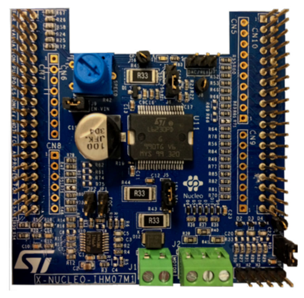
Figure 2.
Electric representation of the X-NUCLEO-IHM07M1 board in PLECS simulator.
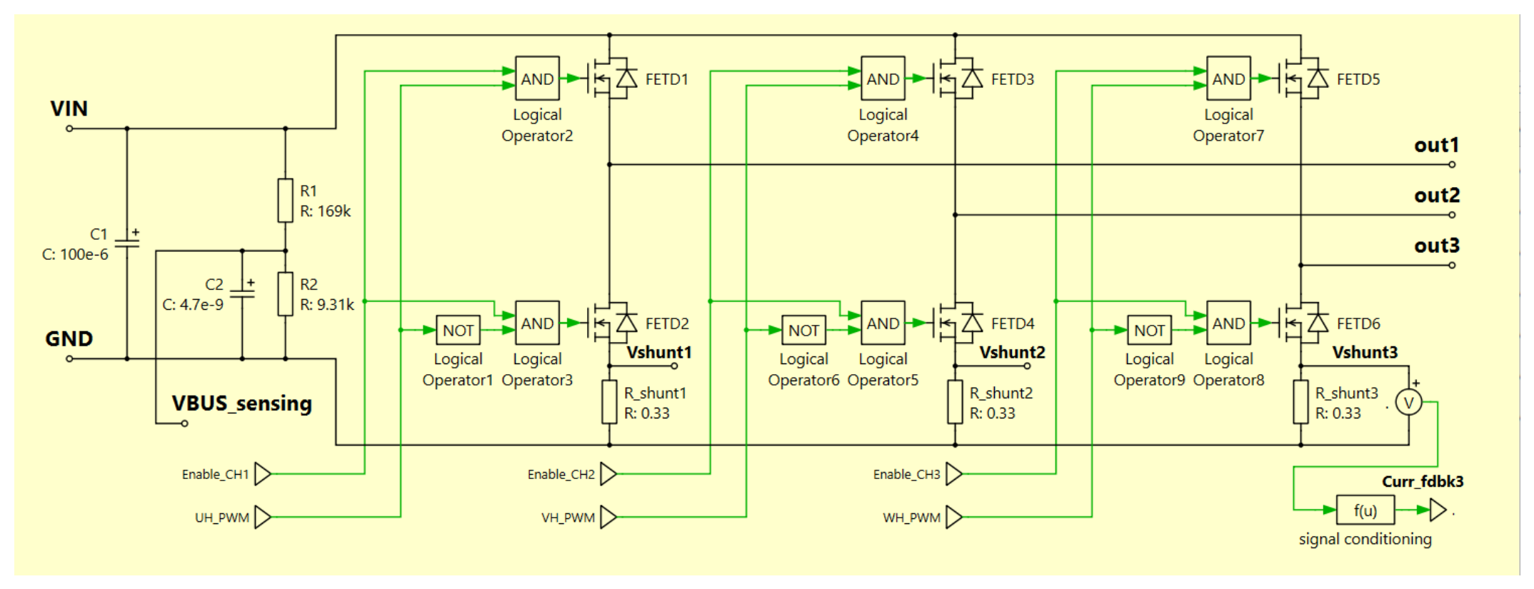
Figure 3.
Schematic of the current signal conditioning circuit.
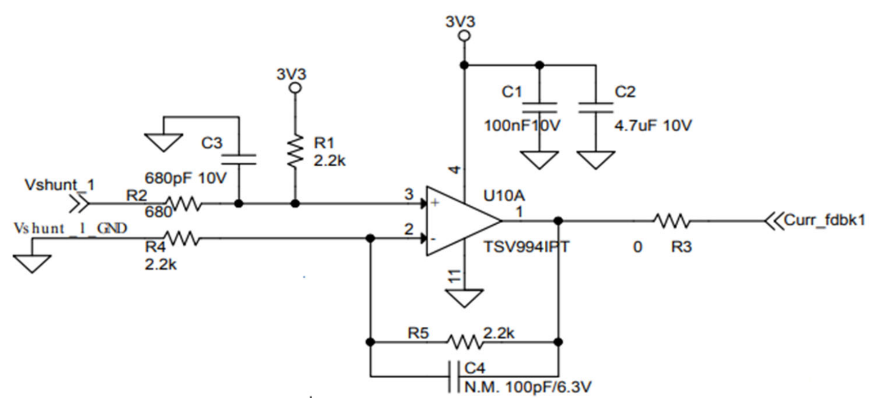
Figure 4.
Schematic of the voltage signal conditioning circuit.
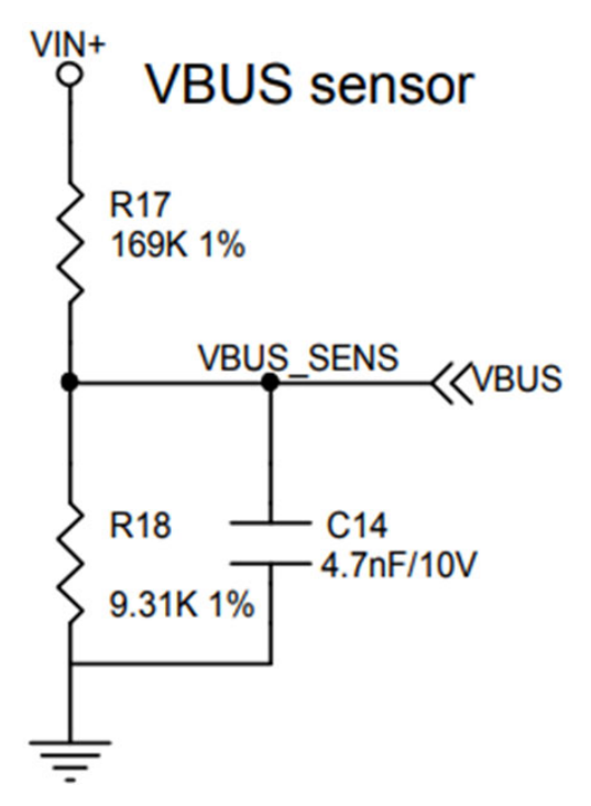
Figure 5.
Example of DAVE™ Apps utilization and connection.
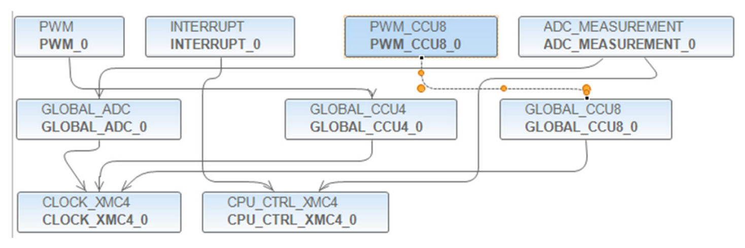
Figure 6.
Example of DAVE™ Apps: PWM_CCU8 App.
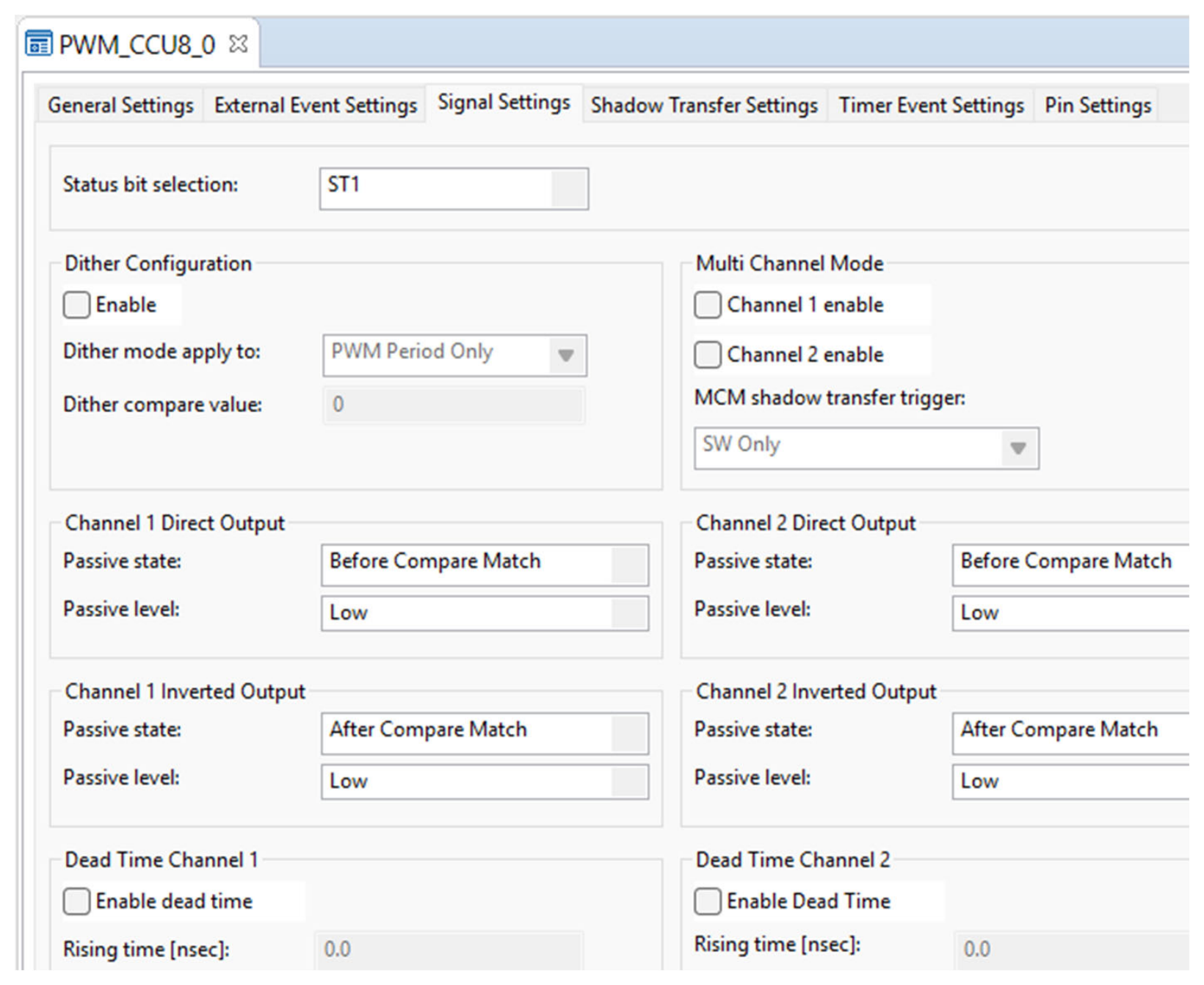
Figure 7.
Example of Micrium μC/Probe XMC GUI.
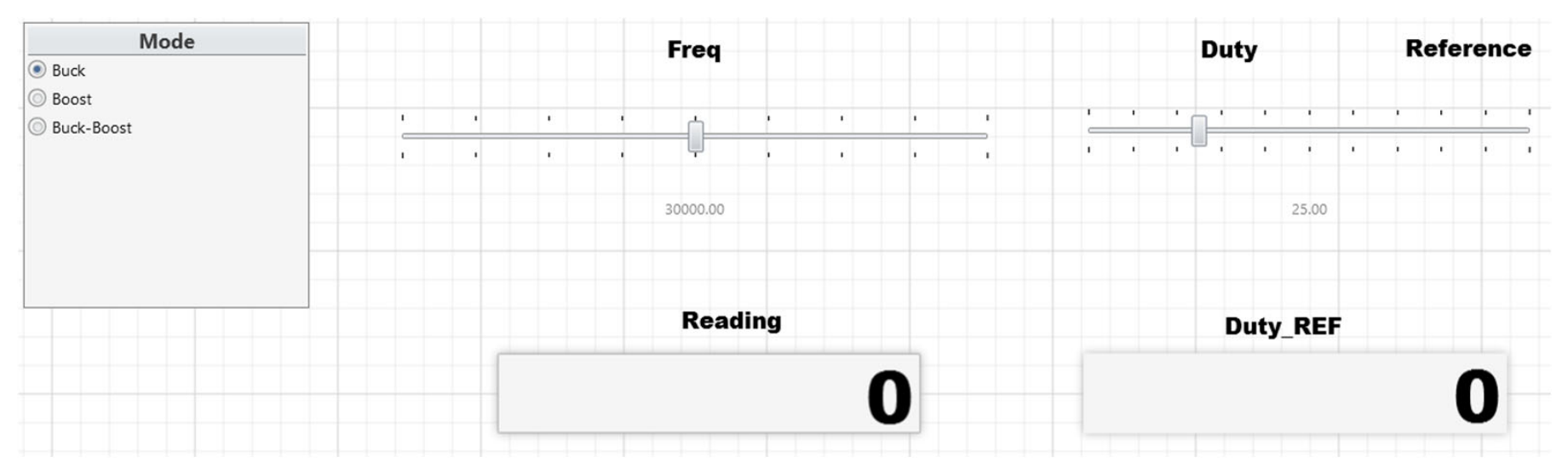
Figure 8.
Example of closed-loop control implementation with C-Script.
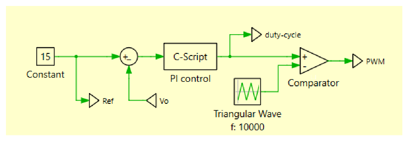
Figure 9.
Example C-Script block details.
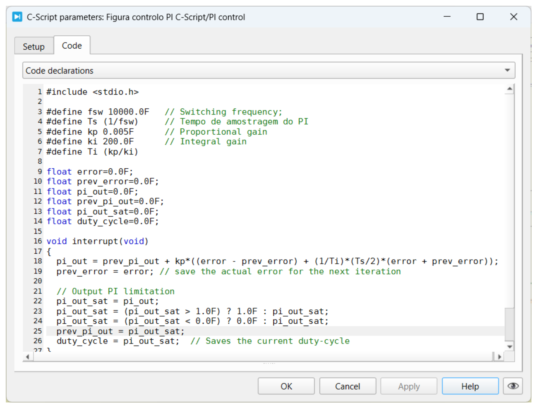
Figure 10.
Generic closed-loop architecture of a power converter.
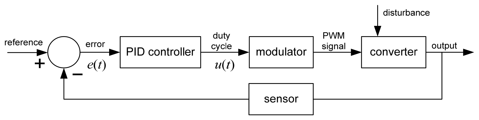
Figure 11.
Sampling architecture diagram.
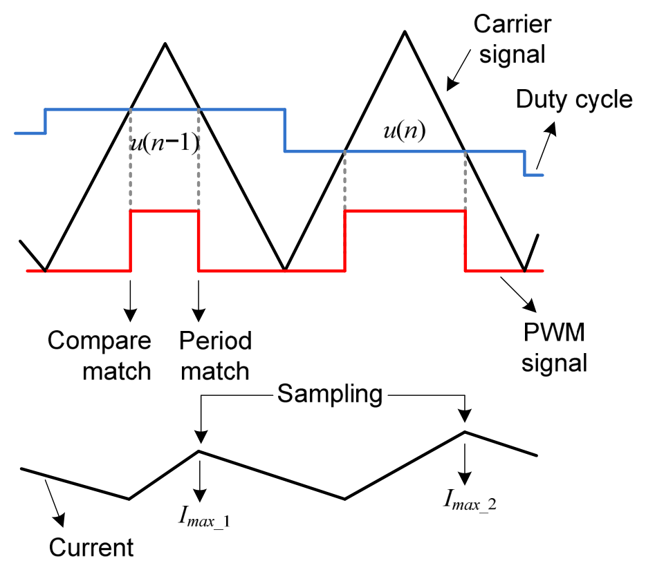
Figure 12.
(a) Hardware signal connection between PWM and ADC_MEASUREMENT; (b) Interrupt handler configuration.
Figure 12.
(a) Hardware signal connection between PWM and ADC_MEASUREMENT; (b) Interrupt handler configuration.
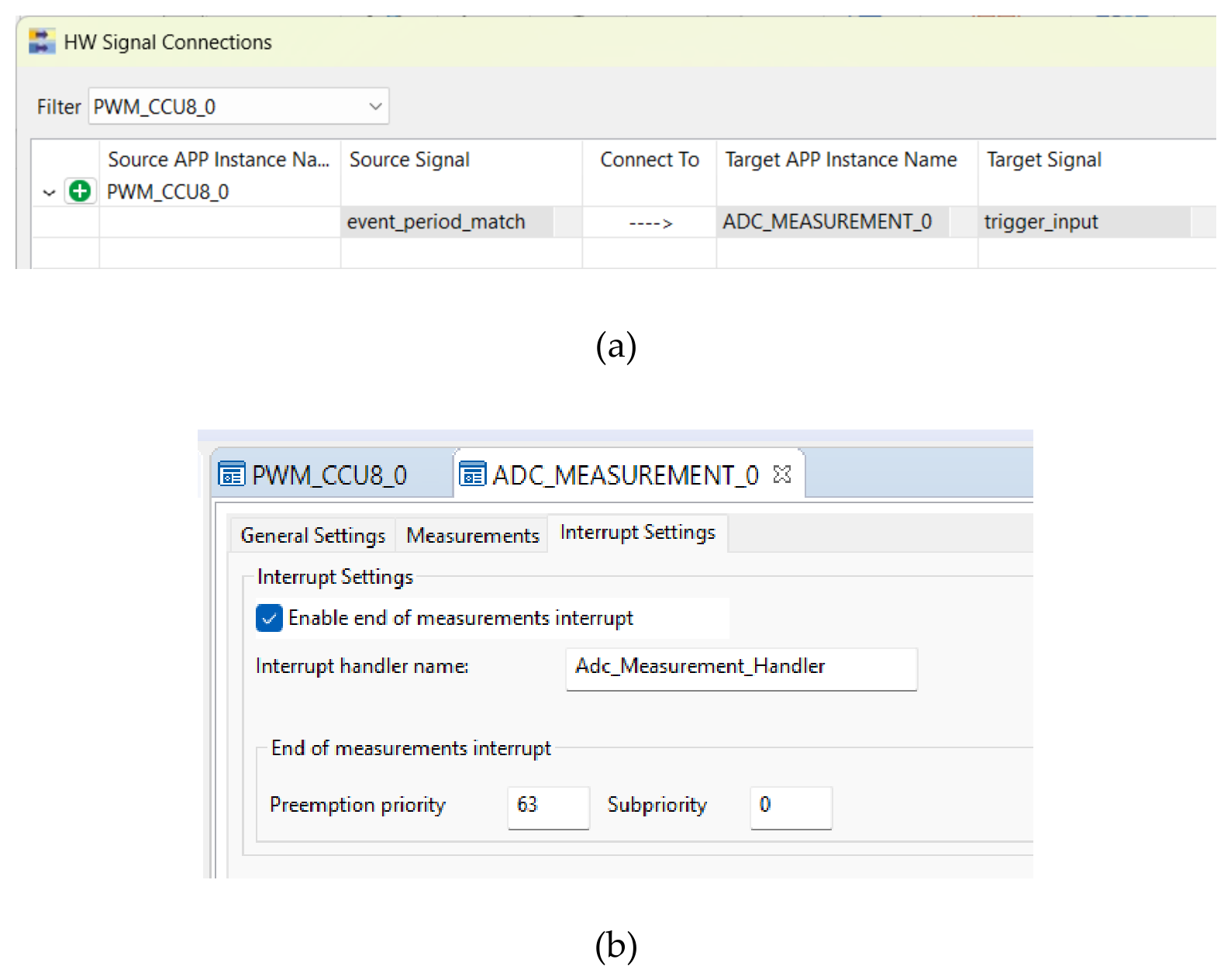
Figure 13.
Electrical representation of the boost converter in the PLECS simulator.
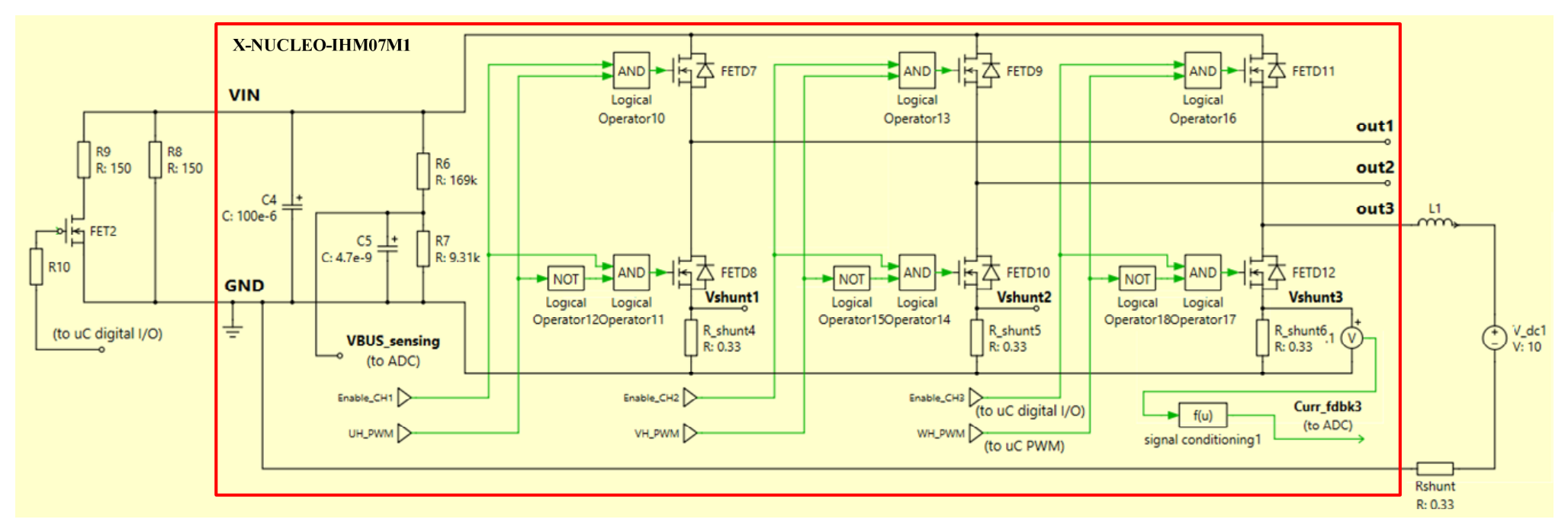
Figure 14.
Overview of the experimental setup for boost converter.
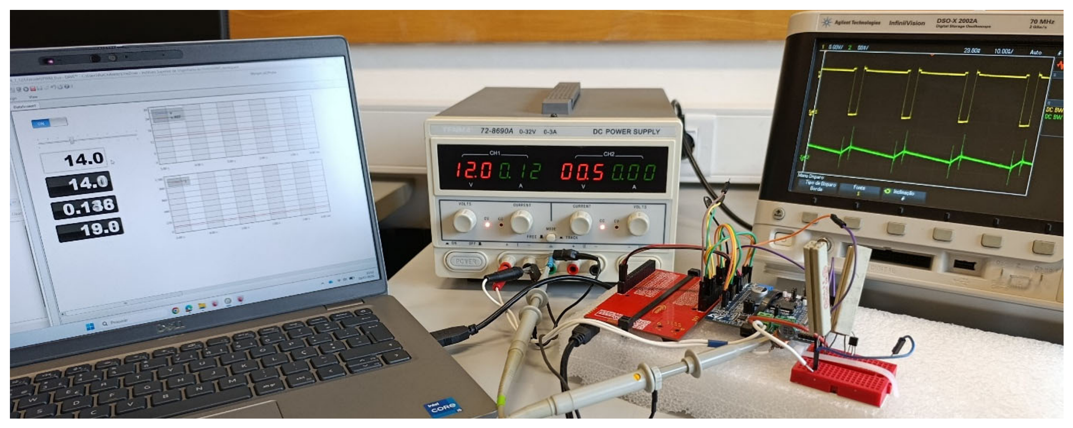
Figure 15.
Output voltage waveforms: DC component (orange) and AC ripple component (green).
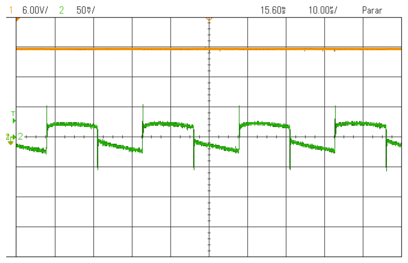
Figure 16.
Waveforms of Drain-Source voltage (orange) and inductor current (green).
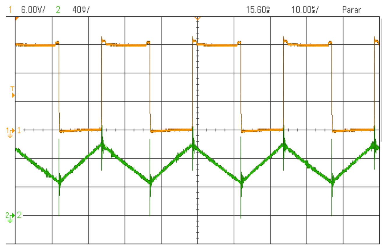
Figure 17.
Output voltage (orange) and inductor current (green) when the reference voltage changes from 12 V to 18 V (current scale 0.33 V/A).
Figure 17.
Output voltage (orange) and inductor current (green) when the reference voltage changes from 12 V to 18 V (current scale 0.33 V/A).
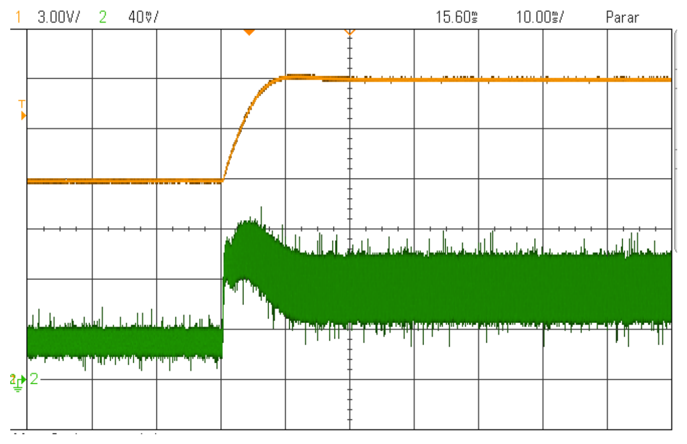
Figure 18.
Output voltage (orange) and inductor current (green) when the load changes from 150 Ω to 75 Ω (current scale 0.33 V/A).
Figure 18.
Output voltage (orange) and inductor current (green) when the load changes from 150 Ω to 75 Ω (current scale 0.33 V/A).
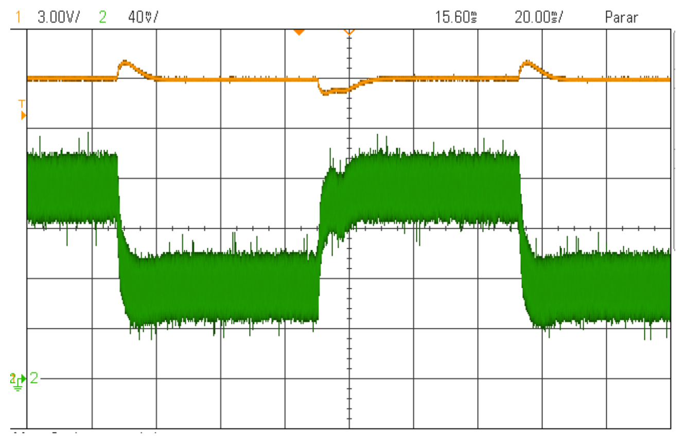
Figure 19.
Electrical representation of the H-brigde for DC motor speed control in the PLECS simulator.
Figure 19.
Electrical representation of the H-brigde for DC motor speed control in the PLECS simulator.
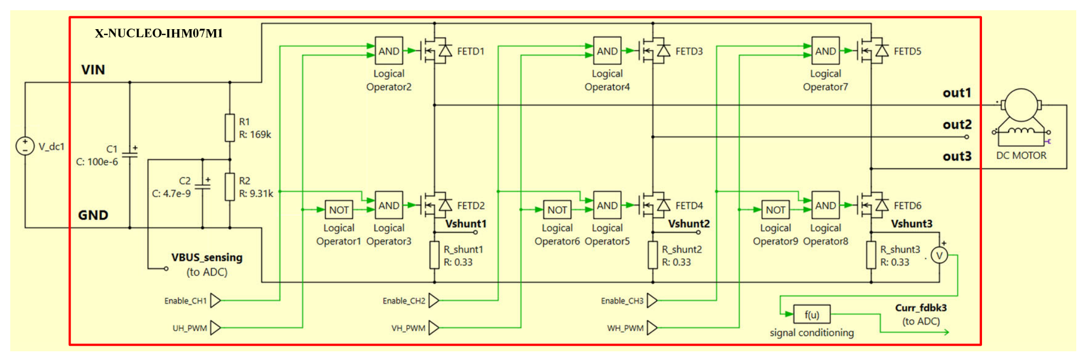
Figure 20.
Control structure for DC motor speed control.

Figure 21.
Overview of the experimental setup for DC motor control.
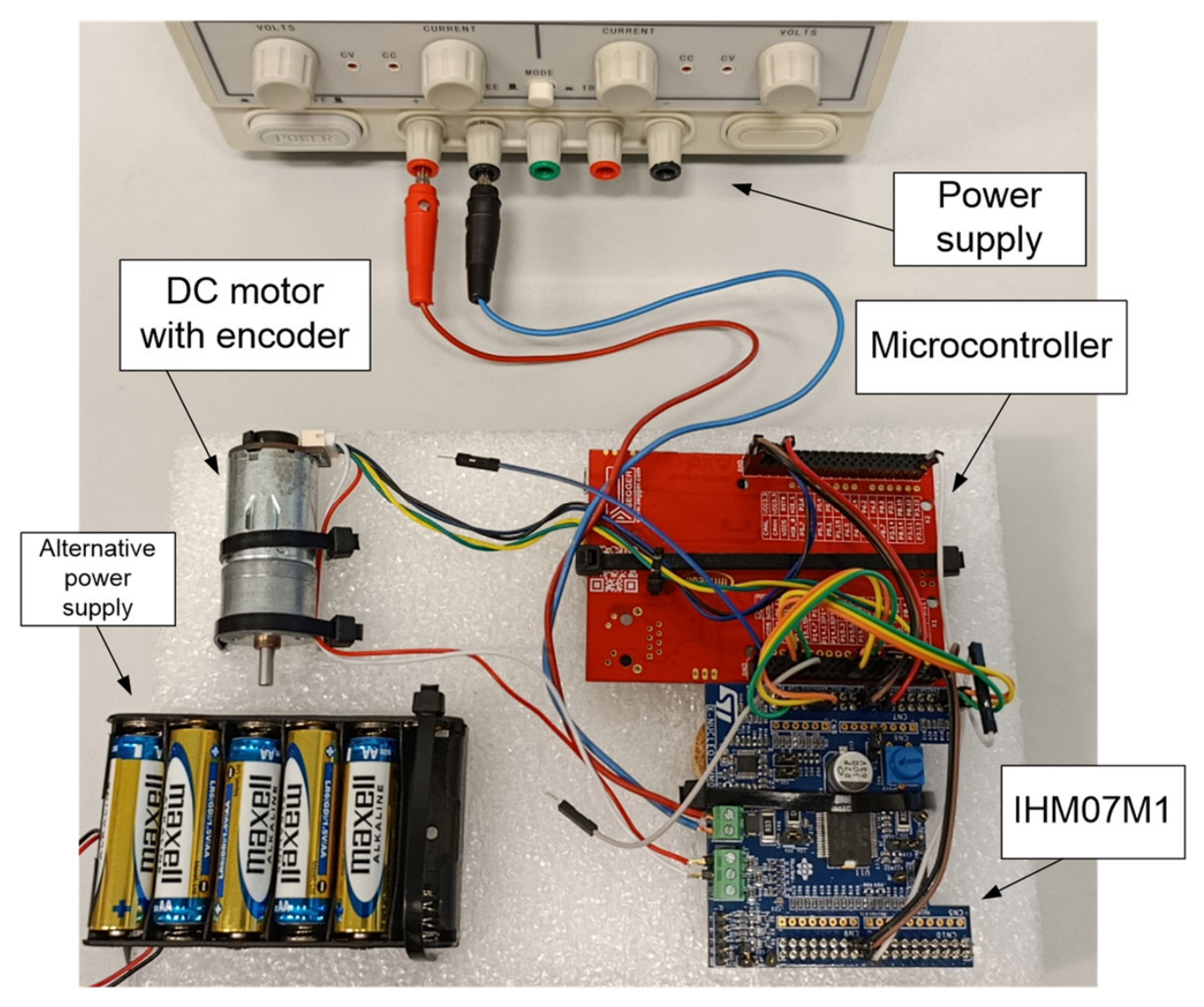
Figure 22.
Speed motor at startup. Reference changes from 0 to 4000 rpm. Reference (blue), actual speed (red).
Figure 22.
Speed motor at startup. Reference changes from 0 to 4000 rpm. Reference (blue), actual speed (red).
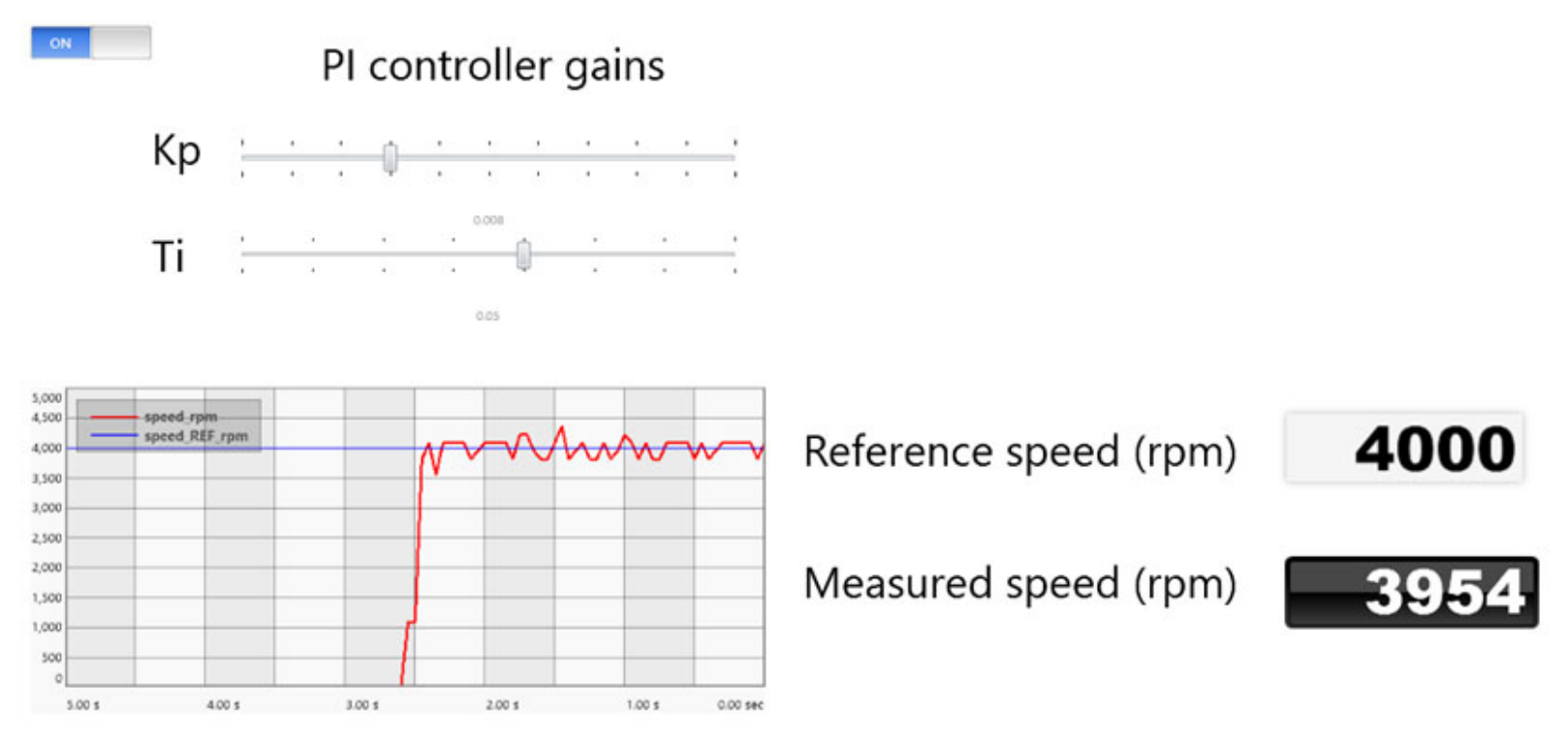
Figure 23.
Speed reference (blue) and actual speed (red) when the reference changes from 1000 rpm to 4000 rpm.
Figure 23.
Speed reference (blue) and actual speed (red) when the reference changes from 1000 rpm to 4000 rpm.
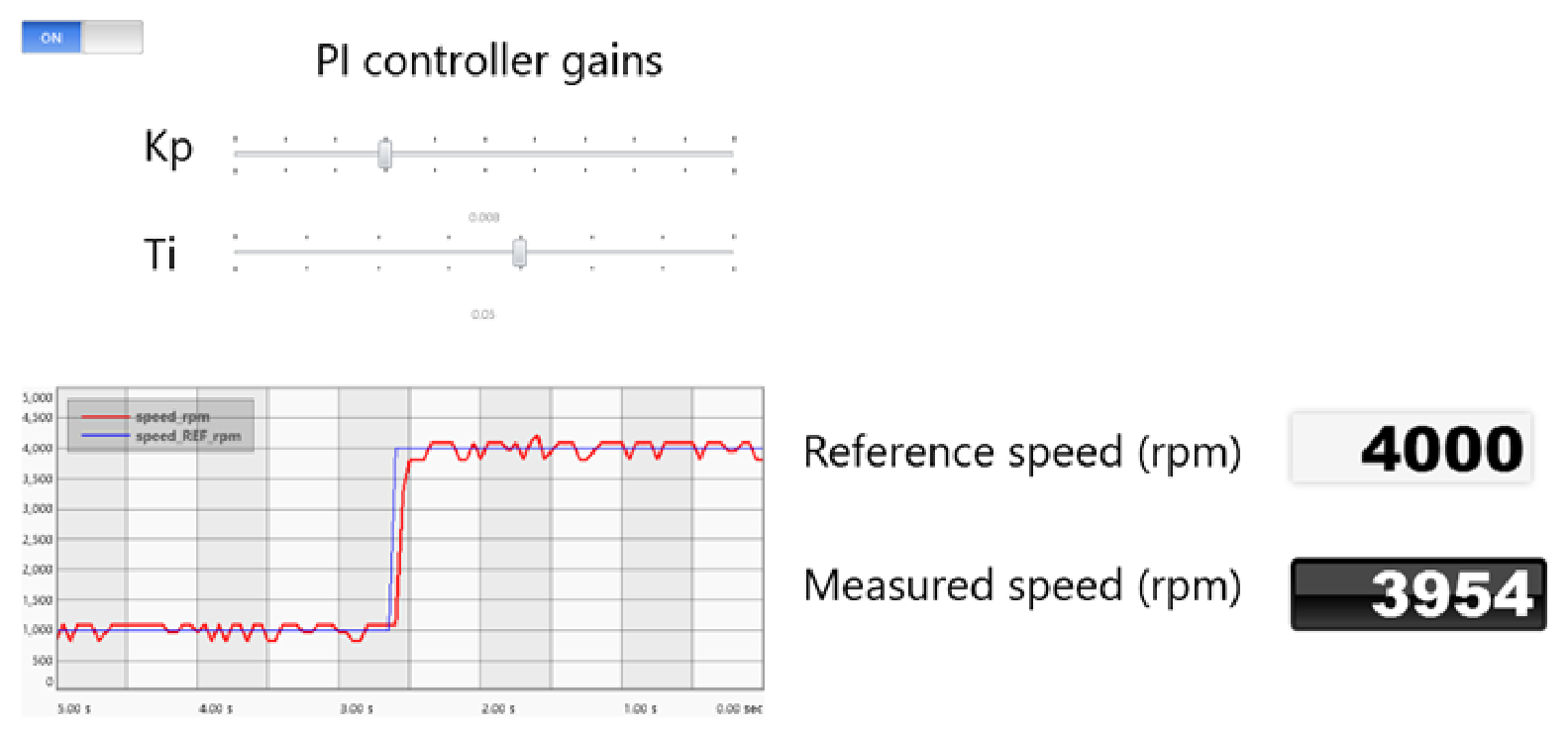
Figure 24.
Speed reference (blue) and actual speed (red) when the reference changes from 4500 rpm to 2500 rpm.
Figure 24.
Speed reference (blue) and actual speed (red) when the reference changes from 4500 rpm to 2500 rpm.
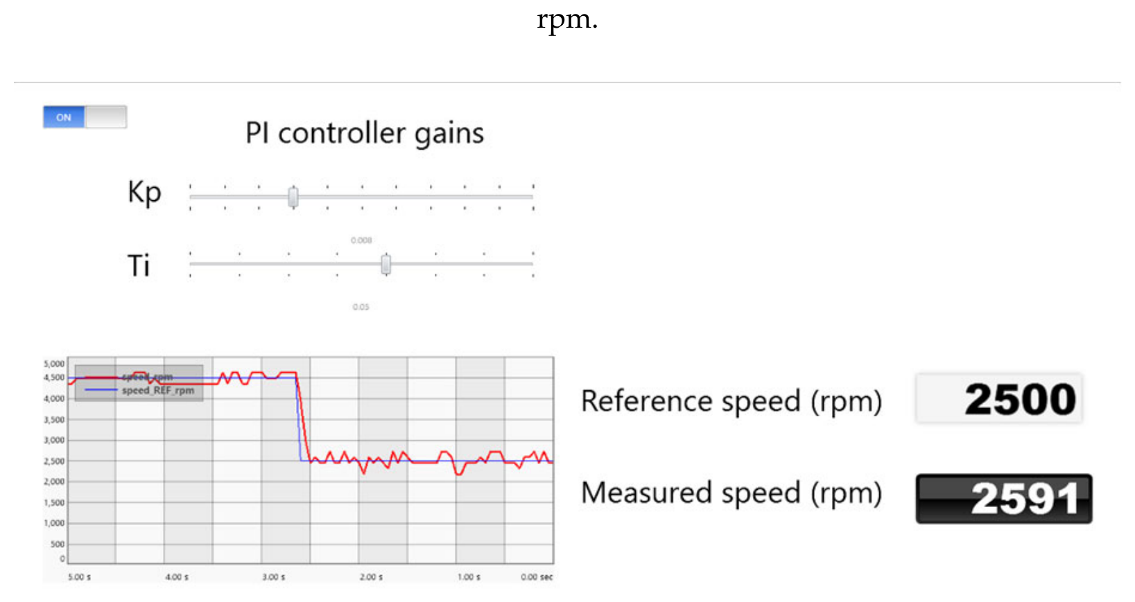
Figure 25.
Electrical representation of the three-phase inverter in the PLECS simulator.
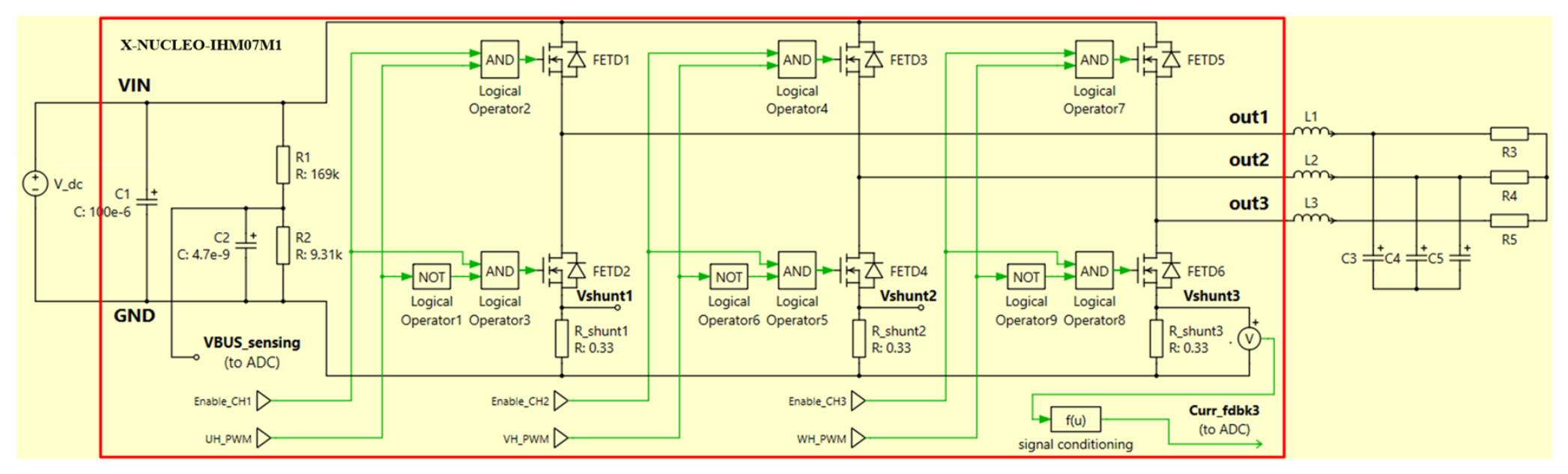
Figure 26.
Line-to-neutral voltage waveforms without LC filter (m = 0.9).
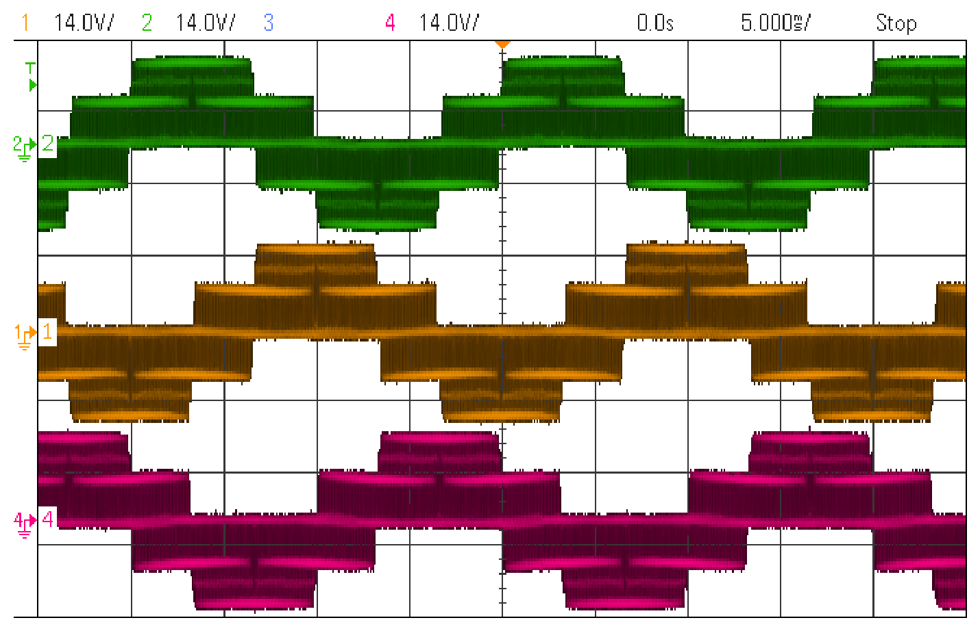
Figure 27.
Line-to-line voltage waveforms without LC filter (m = 0.9).
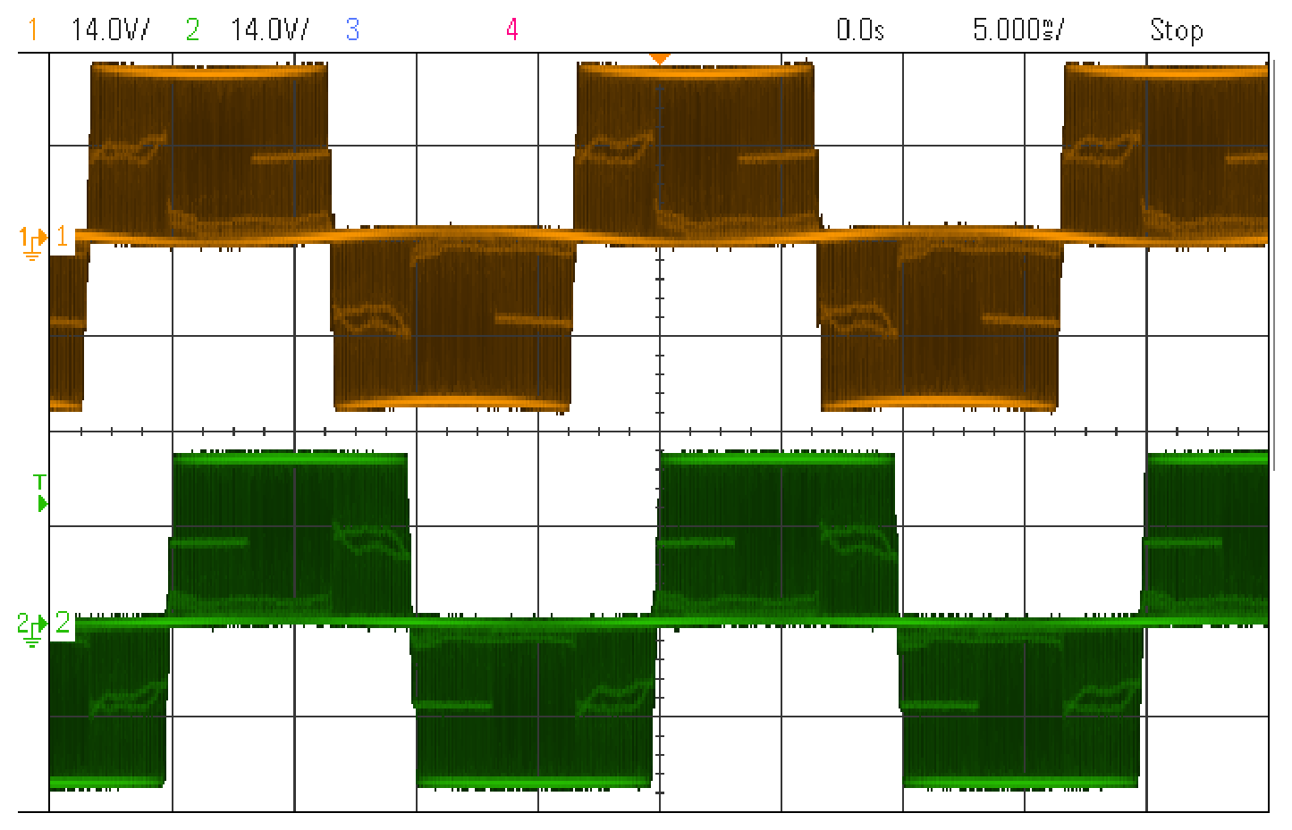
Figure 28.
Line-to-neutral voltage waveforms with LC filter (m = 0.9).
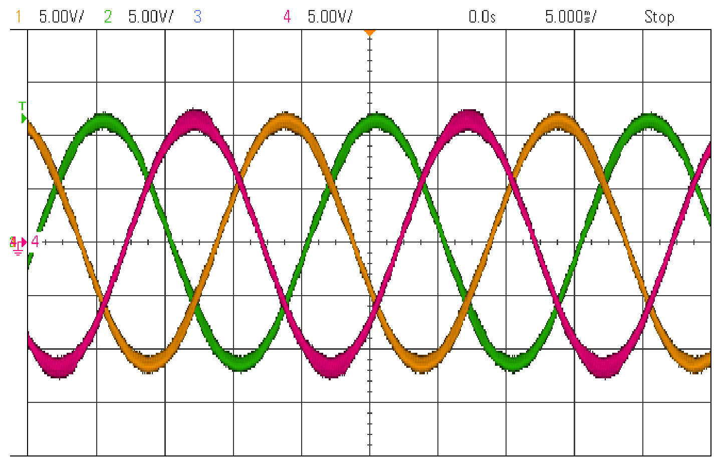
Figure 29.
Line-to-line voltage waveforms with LC filter (m = 0.9).
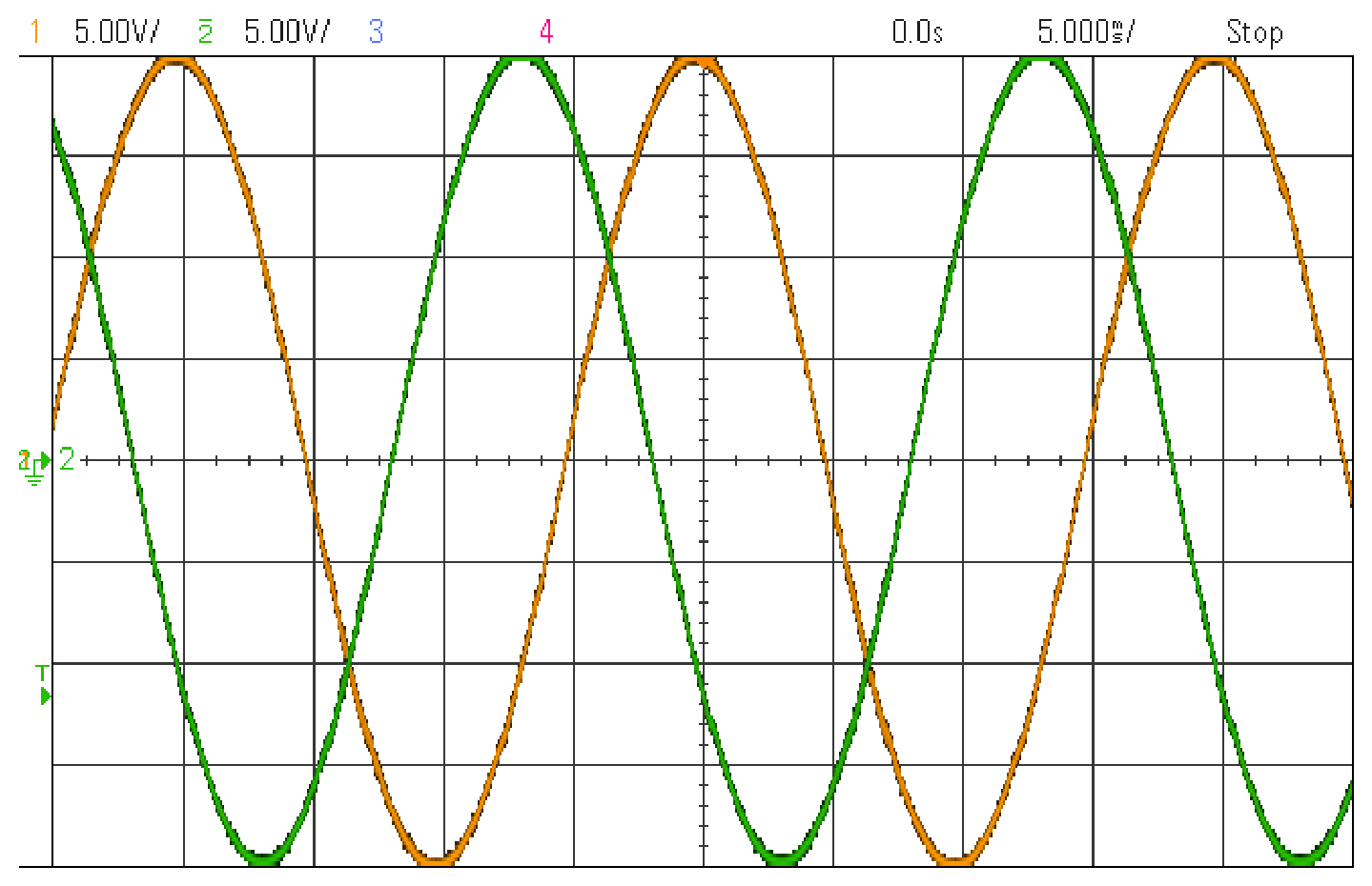

Table 1.
Main X-NUCLEO-IHM07M1 signals and functions.
| Header Pin | Signal Name | Function |
| CN10 - Pin 23 | UH_PWM | Phase A High PWM Input |
| CN10 - Pin 21 | VH_PWM | Phase B High PWM Input |
| CN10 - Pin 33 | WH_PWM | Phase C High PWM Input |
| CN7 - Pin 1 | Enable_CH1 | Phase A Bridge Enable |
| CN7 - Pin 2 | Enable_CH2 | Phase B Bridge Enable |
| CN7 - Pin 3 | Enable_CH3 | Phase C Bridge Enable |
| CN7 - Pin 28 | Curr_fdbk_PhA | Phase A Current Sensing Output |
| CN7 - Pin 36 | Curr_fdbk_PhB | Phase B Current Sensing Output |
| CN7 - Pin 38 | Curr_fdbk_PhC | Phase C Current Sensing Output |
| CN7 - Pin 30 | VBUS_sensing | DC Link Bus Voltage Sensing |
Disclaimer/Publisher’s Note: The statements, opinions and data contained in all publications are solely those of the individual author(s) and contributor(s) and not of MDPI and/or the editor(s). MDPI and/or the editor(s) disclaim responsibility for any injury to people or property resulting from any ideas, methods, instructions or products referred to in the content. |
© 2026 by the authors. Licensee MDPI, Basel, Switzerland. This article is an open access article distributed under the terms and conditions of the Creative Commons Attribution (CC BY) license (http://creativecommons.org/licenses/by/4.0/).
Copyright: This open access article is published under a Creative Commons CC BY 4.0 license, which permit the free download, distribution, and reuse, provided that the author and preprint are cited in any reuse.