

Submitted:
02 September 2026
Posted:
03 September 2026
You are already at the latest version
Abstract
The feasibility of executing learned line-segment detectors on microcontroller-class hardware has remained an open question, despite their proven accuracy on graphics processors and the emergence of compact variants such as MiLSD that is ostensibly sized for embedded memory budgets. This work proposes FOLD (Framework for On-Device Line-Segment Detection), an end-to-end deployment methodology for fully-convolutional line detectors. The framework bridges the gap between network representation and on-chip execution across the STM32 family. It is validated on actual hardware at four operating points: a 25k-parameter F-Clip baseline on an STM32F746, MiLSD across four STM32H7 boards, and two NPU-native detectors (NPLSD-M and NPLSD-H) on an STM32N6.On the STM32H7B3, int8 MiLSD runs at 10.6 s per inference with an 847 KB on-chip arena. The same model cannot be deployed on the faster STM32H743 due to fragmented SRAM, confirming that memory layout, not capacity, governs deployability. On the NPU class, a key finding is that int8 quantization, not a convolutional graph alone, engages the accelerator. In int8, NPLSD-H runs in 33.7 ms at sAP10=35.9 entirely in on-chip SRAM, a 698× speedup over MiLSD. NPLSD-M reaches sAP10=41.1 in 121.7 ms. The framework yields a measured tier map from CPU-only boards to a real-time NPU operating point. An edge-GPU reference (LINEA-N on Jetson Xavier NX: sAP10=63.9 at 101 ms, 1.34 J) bounds the map from above. All on-chip outputs match the reference models to cosine 1.000.
Keywords:
line segment detection (LSD)
; TinyML
; STM32
; neural accelerator
; edge AI
1. Introduction
Line segment detection (LSD) serves as a fundamental component in visual SLAM, structure-from-motion, and industrial inspection. Lines become particularly valuable in environments where point features are scarce. Point-line SLAM systems [1,2] have been shown to be markedly more robust than point-only pipelines in low-texture, man-made indoor scenes. Such scenes are typical of mobile robots and drones, platforms that would benefit considerably from performing detection on the device itself rather than streaming imagery to a remote host. Modern learned detectors achieve high accuracy, yet they assume graphics processors or, at best, mobile-class application processors [3,4,5]. Even the lightest reported model requires tens of megabytes of runtime memory [6]. MiLSD was recently introduced as a compact int8 line-segment detector sized explicitly for microcontroller memory budgets [7]. It reaches a structural average precision of on the ShanghaiTech Wireframe benchmark within a MB activation budget. As an algorithmic result, however, its execution on hardware had not been demonstrated prior to this work.
This work introduces FOLD, a reusable framework for deploying convolutional line detectors on STM32 microcontrollers, and measures it on real silicon at four distinct operating points. The first operating point is F-Clip-25k on the STM32F746, a MHz Cortex-M7 with only KB of SRAM. This establishes the lower end of the deployment envelope. The second is MiLSD on the STM32H7 family, a 280 MHz to MHz Cortex-M7 with approximately MB of SRAM and no hardware accelerator. Inference runs in int8 through CMSIS-NN [8]. The decoder is implemented as a lightweight on-chip post-processing pass. The third and fourth are NPLSD-H and NPLSD-M on the STM32N6, a Cortex-M55 paired with the Neural-ART NPU [9]. The accelerator is a convolution engine. Transformer-based detectors therefore derive no benefit from it. The two NPLSD variants are fully-convolutional, NPU-native detectors, one built on a dense HGNetv2 trunk and one on a depthwise MobileNetV2 trunk, whose every operator is mapped onto the accelerator. They give the N6 tier a measured speed-versus-accuracy choice. A final measurement leaves the STM32 envelope. LINEA-N, a M-parameter transformer detector, is deployed on an NVIDIA Jetson Xavier NX exactly as released and measured under the same protocol. This edge-GPU reference tier bounds FOLD from above and prices, in measured joules, the distance between an MCU-integrated NPU and a commodity GPU module.
The contributions of this paper are as follows:
- FOLD is introduced: a single free and reproducible deployment framework for line detectors on STM32, spanning export, int8 quantization, code generation, on-chip decode, and on-target measurement.
- The first on-device characterization of learned line-segment detection on a microcontroller is presented. It spans the no-NPU (H7) and NPU (N6) classes, bounded from above by a measured edge-GPU reference (LINEA-N on a Jetson Xavier NX). Measured metrics include flash, peak SRAM, per-layer latency, throughput, and estimated energy; on the GPU tier, board power is measured directly.
- A memory-layout finding is established: on-chip deployability is decided by the largest contiguous SRAM region, not the nominal SRAM total. This observation is generalized across four STM32H7 boards.
- Two NPU-class findings are measured on the STM32N6: int8 quantization, not graph convolutionality, is what engages the accelerator ( and float-to-int8 speedups on two independent graphs); and parameter count predicts neither latency nor memory residency, since the smaller depthwise variant runs slower and spills to external RAM while the dense variant runs fully on-chip in real time.
The remainder of this paper is organized as follows. Section 2 reviews related work. Section 3 describes the target platforms. Section 4 presents FOLD itself. Section 5 details the three device deployments. Section 6 reports the measured results. Section 7 and Section 8 provide discussion and concluding remarks.
2. Background and Related Work
2.1. Learned Line-Segment Detection
End-to-end parsing of line segments has been pursued by a number of modern detectors. L-CNN [3] detects junctions and verifies candidate lines through a Line-of-Interest head. HAWP and its successor [4,10] incorporate a holistic attraction field. F-Clip [5] eliminates junctions entirely and predicts each line’s center, length, and angle in a single fully-convolutional stage. Transformer-based detectors have pushed accuracy further. Examples include LETR [11], DT-LSD [12] (which reports ), and LINEA [13]. These models, however, come at a higher computational cost. On the efficiency front, M-LSD [6] was designed for mobile phones, and EM-LSD [14] is a recent lightweight design with M parameters. Both still require tens of megabytes of runtime memory and assume a GPU or mobile-class SoC. FOLD adopts the F-Clip representation (center, length, and angle) precisely because it is single-stage and fully convolutional. This property makes on-chip decode and quantized microcontroller execution tractable, including on a convolutional NPU.
2.2. Detectors Deployed in This Work
F-Clip-25k is a minimal variant of F-Clip with 25k parameters. It serves as a lower-bound baseline.

Table 1.
Target microcontrollers. The last row is the edge-GPU reference tier, outside the STM32 envelope.
Table 1.
Target microcontrollers. The last row is the edge-GPU reference tier, outside the STM32 envelope.
| Device | Core | SRAM | Flash | NPU |
|---|---|---|---|---|
| STM32F746 | M7 @216 MHz | 320 KB | 1 MB | — |
| STM32H7B3 | M7 @280 MHz | 1 MB (contig.) | 2 MB | — |
| STM32H743 | M7 @480 MHz | 1 MB (frag.) | 2 MB | — |
| STM32N6 | M55 @800 MHz | ∼4.2 MB | ext. | Neural-ART |
| Jetson Xavier NX | 6×Carmel @1.4 GHz | 16 GB LPDDR4x | 16 GB eMMC | Volta GPU (384-core) |
MiLSD [7] is an int8 fully-convolutional detector that adopts the F-Clip representation on a backbone of approximately M parameters. The backbone is sized to a 1 MB activation arena. MiLSD incorporates sub-pixel decoding, test-time augmentation, and a Line-of-Interest verification head. It achieves on the Wireframe benchmark.
NPLSD-H and NPLSD-M are two NPU-native detectors built entirely from the Neural-ART operator set, one on a dense HGNetv2-B0 trunk and one on a depthwise M-LSD-tiny trunk. Their design, training, and accuracy analysis are given in a separate publication [15]; Section 5.3 states the properties relevant to deployment.
2.3. TinyML and On-Device Inference
On a microcontroller, the binding constraint is peak activation memory rather than parameter count [16,17]. Int8 quantization [18] and optimized integer kernels (CMSIS-NN [8]) have made convolutional inference feasible on Cortex-M class processors. The STM32N6 adds the Neural-ART NPU [9,19], a convolution-oriented accelerator. A vendor-provided compilation flow handles analysis, quantization, code generation, and on-target benchmarking. On the N6, it maps supported operators onto the accelerator. Section 4 names the exact tool versions used in this work. Standardized microcontroller inference benchmarks, such as MLPerf Tiny [20], typically cover keyword spotting, image classification, anomaly detection, and person detection. These are lightweight tasks with scalar or low-dimensional outputs. Line-segment detection is substantially heavier. It produces a dense, structured output over the full image grid. Its on-device cost is therefore not captured by existing benchmark suites. This gap is part of what motivates the measurement study reported in this paper.
3. Target Platforms
Table 1 lists the STM32 devices covered in this work. The STM32F746 [21] is the most constrained device with KB of SRAM. It hosts the 25k-parameter baseline. The STM32H7 line provides roughly an order of magnitude more SRAM, which enables MiLSD. As discussed in Section 5, however, placement is determined by the contiguity of that SRAM rather than its total size. The STM32N6 adds the Neural-ART NPU [9], which enables the NPU-native NPLSD-H. None of the devices requires an external accelerator or host processor. One non-STM32 device completes the table: a Jetson Xavier NX module (six Carmel cores, a 384-core Volta GPU, and 16 GB of shared LPDDR4x) [22] stands in for the commodity edge-GPU class as the reference tier of Section 5.4.
4. The FOLD Framework
FOLD is identical across all devices and entirely free of licensing costs. The only hardware expense is the board itself. Training is performed off-device; the microcontroller runs only quantized inference. This follows the train-off / infer-on paradigm.
4.1. Export and int8 Quantization
Each trained model is exported from PyTorch to ONNX at a fixed input resolution. The recommended PyTorch-to-STM32 flow does not import a PyTorch-native quantized graph directly. The fp32 ONNX model is therefore quantized to int8 using ONNX Runtime static post-training quantization in the tensor-oriented QDQ format. Calibration is performed on a few hundred images from the Wireframe dataset. Models trained with quantization-aware training retain full-precision accuracy after int8 quantization. The quantization process reduces the weight size by approximately a factor of four. ST Edge AI Core v4.0.1 is used throughout. The int8 ONNX model is imported into ST Edge AI (X-CUBE-AI) [23], which analyzes the model, validates it against the ONNX outputs, and generates C code. On the STM32N6, the same tool maps supported operators onto the Neural-ART NPU.
4.2. On-Chip Inference and Decode
The generated runtime exposes the network as a single ai_network_run call. This call operates on an input buffer, an output buffer, and a single activation arena. Turning network outputs into line segments is handled by a small arithmetic post-pass that runs on the MCU after inference. For the F-Clip, MiLSD, and NPLSD outputs, the center map is first dequantized. A max-pool non-maximum suppression step selects center peaks above a confidence threshold. For each selected peak, the length and angle maps provide a half-vector , which yields the two endpoints. A one-dimensional parabolic fit refines each peak to sub-pixel accuracy. MiLSD’s Line-of-Interest verification head is a small per-candidate multilayer perceptron. It operates on features pooled along each line and is evaluated on-chip.
4.3. Measurement Methodology
Flash and peak-SRAM figures are obtained from the toolchain’s analysis report. On-target latency is measured on the physical boards through the toolchain’s validate-on-target flow [23]. Energy per inference is computed as power multiplied by latency. On the Jetson reference tier, board power is read from the module’s on-board sensor during sustained inference, so its energy cell is a measurement rather than an estimate. Accuracy figures (sAP) are the off-device values for each model. Deployment preserves accuracy up to int8 rounding effects. In practice, the on-target C model reproduces the fp32 ONNX output to a cosine similarity of . MiLSD is bit-exact, and NPLSD-H achieves cosine . Code generation therefore introduces no measurable accuracy loss.
5. Device Deployments
5.1. MiLSD on the STM32H7B3 (No NPU)
MiLSD’s int8 backbone, with approximately M parameters, runs in int8 through CMSIS-NN without any hardware accelerator. The exported int8 backbone ( M parameters) occupies 386 KB of flash. The analysis report gives a peak activation arena of 847 KB at a pixel input. This arena is dominated by the deep convolutions. A negative finding emerged concerning where that arena can reside. The peak requires two simultaneous activation buffers of approximately 512 KB each, corresponding to a convolution’s input and output. On the STM32H743 (480 MHz), the nominal 1 MB SRAM is split into separate domains: a 512 KB AXI-SRAM plus additional regions of at most 288 KB. Only one buffer of that size fits in any single contiguous region. The model therefore cannot be allocated on-chip. On a NUCLEO-H743ZI2, which has no external RAM, the model cannot be placed at all. On-chip deployability is thus determined by SRAM layout rather than total capacity. The STM32H7B3 resolves this issue. Its D1 domain exposes a single contiguous 1 MB AXI-SRAM. On an STM32H7B3I-DK, the 847 KB arena is placed entirely on-chip. Specifically, 768 KB reside in the AXI-SRAM at 0x24000000, and KB are placed in the DTCM. The board’s 16 MB external SDRAM is left unused. On real silicon, a single inference takes ms ( FPS) at 280 MHz. The off-device carries over unchanged. The estimated energy per inference is J (‡ in Table 6). Table 2 and Figure 1 generalize this observation across four STM32H7 boards. MiLSD runs fully on-chip only on the H7B3 with its contiguous 1 MB SRAM. It spills to external SDRAM on the memory-fragmented H747 and the small-internal H7S78. It cannot be placed at all on the NUCLEO-H743. Latency scales with clock frequency, from s at 280 MHz down to s at 600 MHz.
The on-chip H7B3 sustains cycles per MACC, compared to – on the external-RAM H747 and H7S78. This represents a small penalty for executing activations off-chip.
Table 2.
MiLSD across four STM32H7 boards ( M parameters, input, int8). All outputs match the ONNX model to cosine .
Table 2.
MiLSD across four STM32H7 boards ( M parameters, input, int8). All outputs match the ONNX model to cosine .
| Board | Core @ Clock | On-chip SRAM | Ext. RAM | Arena placement | Latency (ms) | FPS |
|---|---|---|---|---|---|---|
| STM32H7B3I-DK | M7 @280 MHz | ∼1.2 MB (1 MB contig.) | 16 MB | fully on-chip | ||
| STM32H747I-DISCO | M7 @400 MHz | 1 MB (fragmented) | SDRAM | external (544 KB spilled) | ||
| NUCLEO-H743ZI2 | M7 @480 MHz | 1 MB (fragmented) | none | cannot place | — | — |
| STM32H7S78-DK | M7 @600 MHz | 620 KB (455 KB usable) | 16 MB | external |
5.1.1. Where the Cycles Go
Table 3 decomposes the s H7B3 inference by layer. The workload consists almost entirely of the five convolutions. The two deepest convolutions ( at ) cost 604 MMACC each and take s apiece ( each). With the third 128-channel convolution, these account for of both the multiply-accumulate operations and the wall-clock time. The kernel sustains cycles per MACC ( cycles at 280 MHz). Latency is therefore a near-linear function of MACC count. This is a compute-bound, roofline-limited workload with no accelerator. Beyond the 385 KB of int8 weights, the generated runtime adds only 25 KB of flash and KB of RAM.
5.2. The Lower Bound: F-Clip-25k on the STM32F746
At the small end of FOLD’s range, a minimal 25k-parameter F-Clip variant fits entirely within the STM32F746’s 320 KB SRAM. Its activation arena is 200 KB, and the external SDRAM is left unused. Inference runs in 679 ms ( FPS) at 216 MHz. The on-chip output matches the ONNX model to a cosine similarity of . The workload profile is convolution-dominated, with the two deepest convolutions accounting for of the runtime. This operating point anchors the low end of the accuracy-cost frontier (Section 6).
5.3. NPLSD on the STM32N6 (Neural-ART NPU)
The most accurate line detectors currently available are transformer-based. LINEA-N, for example, achieves [13]. A microcontroller equipped with an NPU would appear to be the natural platform for raising the on-device accuracy ceiling. For transformer detectors, however, this expectation does not hold. The reason is architectural. The Neural-ART is a convolution accelerator. A transformer detector’s non-convolutional operators have no accelerator primitive. These include the deformable GridSample at the core of line-attention, LayerNorm, the attention Softmax, and TopK/Gather for query selection. Such operations execute on the Cortex-M55. In addition, the decoder’s self-attention over queries alone exceeds the on-chip activation budget. In practice, only LINEA-N’s backbone is deployable, and it runs approximately in software with the NPU idle. The accelerator is therefore wasted on a transformer. What the same detector achieves on hardware built for it is measured in Section 5.4. Table 4 summarizes operator support across the deployment targets.
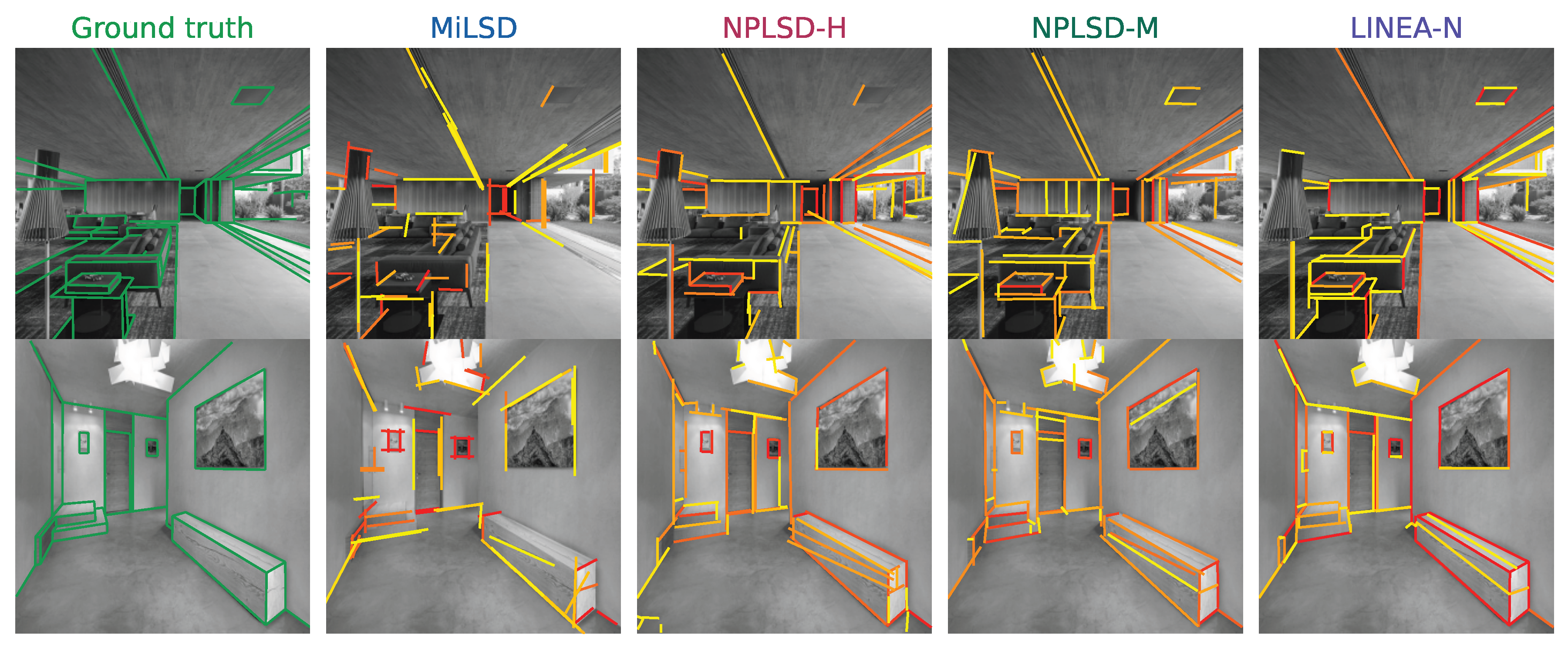
The NPLSD pair is deployed instead: two fully-convolutional, NPU-native detectors co-designed for the accelerator. NPLSD-H retains the convolutional HGNetv2-B0 backbone [24,25] and replaces the transformer encoder-decoder with a convolutional feature pyramid and an F-Clip dense head ( M parameters, warm-started, 35.9 in int8). NPLSD-M rebuilds the depthwise M-LSD-tiny trunk for the same head ( M parameters, , 41.1 in int8). Every operator in both designs, convolution, ReLU or its bounded Clip form, addition, concatenation, nearest-neighbour resize, and max-pool, maps onto the Neural-ART NPU. Qualitative results are shown in Figure 3. The architectures and training procedures are detailed in the companion paper [15].
Deployment on an STM32N6570-DK follows the same FOLD toolflow, with a static-shape simplification and a stem-pad fold to satisfy the accelerator compiler. NPLSD-H reproduces its reference output on-chip to cosine (signal-to-noise ratio of 121 dB); the int8 binaries reproduce their quantized ONNX references to cosine 0.9974 (H) and 0.9991 (M), the expected int8 rounding scale. Code generation therefore introduces no measurable drift. The measured values are collected in Table 5. NPLSD-H has M parameters and GMACC at input resolution. Int8 quantization reduces the weights from MB (float) to MB. A key finding is that int8 quantization is what engages the accelerator. When left in floating point, the network compiles to a native-float graph of 109 epochs (93 software, 9 hybrid, and only 7 pure hardware). On-target measurement shows that of the runtime executes on the Cortex-M55 at s per inference, with the NPU essentially idle ( of runtime).
The integer accelerator cannot execute float convolutions. This is the native-float fallback, not an NPU result. In float, the activation working set is MB. Only MB stays in internal SRAM, while MB spills to external hyperRAM. The weights occupy MB of external octoFlash. This echoes, on the NPU class, the same internal-versus-external placement pressure observed on the H7 family. Int8 removes it for the dense trunk. The quantized NPLSD-H runs in ms per inference ( inferences per second), a speedup over its own float fallback, with of the runtime on the NPU and zero pure-software epochs (72 hardware, 6 hybrid). Its MB activation arena resides entirely in internal SRAM, with no external RAM traffic at all: the first configuration of this work to run fully on-chip on the N6. Figure 2 shows the compiled epoch mapping of all four configurations.
On the same board, int8 NPLSD-M completes an inference in ms ( inferences per second) at a hardware share, 51 of 53 epochs pure hardware and none in software; its 20 Clip nodes execute on the accelerator, confirming the ReLU6 adaptation in silicon. The comparison between the two variants is instructive. Although NPLSD-M carries fewer parameters and against GMACC, it runs slower. Depthwise convolutions offer the MAC array little arithmetic intensity per byte moved, an effect compounded by MB of activations spilling to external hyperRAM. What the smaller model does win is storage and accuracy: 650 KB of flash ( less) and against . On an NPU, parameter count predicts neither latency nor memory residency. The tier map of Section 6 therefore offers the N6 two operating points rather than one winner: NPLSD-H for real-time, fully on-chip operation, NPLSD-M for accuracy and minimal flash. In energy terms the tier change is two orders of magnitude: from an estimated J per inference on the H7B3 to roughly 8 mJ for NPLSD-H and 30 mJ for NPLSD-M on the N6 (‡ in Table 6).
Table 5.
Measured values for NPLSD-H and NPLSD-M on the STM32N6570-DK. Float rows show the native-float fallback; int8 rows are the deployed configurations.
Table 5.
Measured values for NPLSD-H and NPLSD-M on the STM32N6570-DK. Float rows show the native-float fallback; int8 rows are the deployed configurations.
| Quantity | NPLSD-H | NPLSD-M |
|---|---|---|
| Parameters | M | M |
| MACC () | G | G |
| float weights (ext. octoFlash) | MB | MB |
| float latency (fallback) | ms ( NPU) | ms ( NPU) |
| float epochs (SW/hyb/HW) | 93/9/7 | ∼all SW (91 total) |
| float activation RAM | MB ( ext.) | — |
| int8 weights (flash) | MB | MB |
| int8 on-NPU latency | ms ( inf/s) | ms ( inf/s) |
| int8 NPU runtime share | ||
| int8 epochs (HW/hyb/SW) | 72/6/0 | 51/2/0 |
| int8 activation RAM | MB, all internal | MB ( ext.) |
| int8 fidelity (C vs. quant. ONNX) | cosine | cosine |
| Accuracy (int8, deployed) | ||
| Platform | M55 @800 MHz, Neural-ART NPU | |
5.4. The Reference Tier: LINEA-N on a Jetson Xavier NX
How much of the remaining accuracy gap is a hardware question rather than a modeling one? To answer it, the strongest detector family of Section 2 is measured one tier above the microcontrollers, on the cheapest hardware class that runs it natively. LINEA-N [13], a M-parameter transformer detector, is deployed on an NVIDIA Jetson Xavier NX module [22] exactly as released: fp32 PyTorch weights ( MB), no quantization, no operator surgery, no co-design of any kind. The board runs its 20 W six-core profile with locked clocks.
A single inference takes ms (median; inferences per second) and peaks at 210 MB of GPU memory. Half precision brings no gain here ( ms): the workload on this GPU is bound by kernel-launch overhead rather than arithmetic, so the deployed configuration stays fp32. Board power, read from the on-module sensor during sustained inference, is W against W idle. That works out to J per inference, the one energy cell in Table 6 that is measured rather than estimated.
Under the unified evaluation protocol of this work, the deployed graph reaches (// at the 5/10/15 thresholds), consistent with the published , which we reproduce exactly under the authors’ own evaluation stack. Input resolution matters at this tier: feeding the same frames used by the microcontroller deployments costs about six points (), since a 640-input transformer cannot recover detail the capture path never stored. The reference tier presumes a full-resolution camera pipeline.
The comparison with the N6 is the point of the exercise. LINEA-N buys points of over NPLSD-M with zero deployment effort. NPLSD-H remains faster in wall-clock terms and roughly more energy-efficient per inference (∼8 mJ against mJ). Figure 3 adds this tier as its fifth column.
Figure 3.
Qualitative results on two Wireframe validation scenes (#12 and #170). Columns: ground truth (green), MiLSD (no-NPU), NPLSD-H and NPLSD-M (NPU class), and LINEA-N (edge-GPU reference). Detections densify from MiLSD () through NPLSD-H (35.9) and NPLSD-M (41.1) to LINEA-N (63.9). The STM32 columns are raw decoded predictions, reproduced on-chip without drift; the LINEA-N column is the deployed fp32 configuration on full-resolution input.
Figure 3.
Qualitative results on two Wireframe validation scenes (#12 and #170). Columns: ground truth (green), MiLSD (no-NPU), NPLSD-H and NPLSD-M (NPU class), and LINEA-N (edge-GPU reference). Detections densify from MiLSD () through NPLSD-H (35.9) and NPLSD-M (41.1) to LINEA-N (63.9). The STM32 columns are raw decoded predictions, reproduced on-chip without drift; the LINEA-N column is the deployed fp32 configuration on full-resolution input.
6. Results
Table 6 presents the measured on-device cost for the four operating points. Table 7 positions these points on the accuracy-resource frontier. FOLD spans a range in parameter count, from 25k for F-Clip to M for NPLSD-H, across the no-NPU and NPU classes. Accuracy increases from to , while latency decreases from s on the H7B3 to ms on the N6. The Jetson reference row extends the ladder to at ms and prices that step at J per inference, measured on the board.
Further comparisons across tiers reveal insights not immediately apparent from the headline figures. Relative to MiLSD on the H7B3, NPLSD-M achieves an reduction in latency while delivering a 17.0-point accuracy gain. NPLSD-H improves upon the F746 baseline by a factor of 20 in speed, with an accuracy increase of points. Profiling the int8 NPLSD-H binary reveals that two fused hardware meta-epochs dominate the schedule, consuming ms and ms respectively, together accounting for 60% of the ms inference time. The bottleneck has shifted. On the H7, the runtime was dominated by two software convolutions. On the N6, it is concentrated in two accelerator epochs. Further performance improvements would therefore require restructuring those computational blocks rather than relying on a faster core.
Table 6.
On-device cost of the four operating points, plus the edge-GPU reference (LINEA-N on Xavier NX). All cells measured on-target; ‡ denotes estimated.
Table 6.
On-device cost of the four operating points, plus the edge-GPU reference (LINEA-N on Xavier NX). All cells measured on-target; ‡ denotes estimated.
| Detector / Device | Params | Flash | Peak SRAM | Latency | Energy/inf. |
|---|---|---|---|---|---|
| F-Clip / F746 | 0.025 M | 25 KB | 200 KB | 679 ms | J ‡ |
| MiLSD / H7B3 | 0.39 M | 0.38 MB | 847 KB | ms | J ‡ |
| NPLSD-H / N6 | 2.63 M | 2.55 MB | 2.70 MB | ms | ∼8 mJ ‡ |
| NPLSD-M / N6 | 0.62 M | 0.65 MB | 5.02 MB | ms | ∼30 mJ ‡ |
| LINEA-N / Xavier NX | 3.90 M | 15.6 MB | 210 MB (GPU) | ms | J (meas.) |
Table 7.
Accuracy versus device class. on Wireframe for the deployed int8 configuration; latency measured on-target. The LINEA-N row is the deployed fp32 configuration on the Jetson reference tier.
Table 7.
Accuracy versus device class. on Wireframe for the deployed int8 configuration; latency measured on-target. The LINEA-N row is the deployed fp32 configuration on the Jetson reference tier.
| Operating point | Latency | Device class | |
|---|---|---|---|
| F-Clip (25k) | 10.6 | 679 ms | MCU, no NPU (320 KB) |
| MiLSD (this work) | 24.1 | 10,614 ms | MCU, no NPU (1 MB) |
| NPLSD-H (this work) | 35.9 | 33.7 ms | MCU + NPU (N6) |
| NPLSD-M (this work) | 41.1 | 121.7 ms | MCU + NPU (N6) |
| LINEA-N (reference) | 63.9 | 101.1 ms | edge GPU (Xavier NX) |
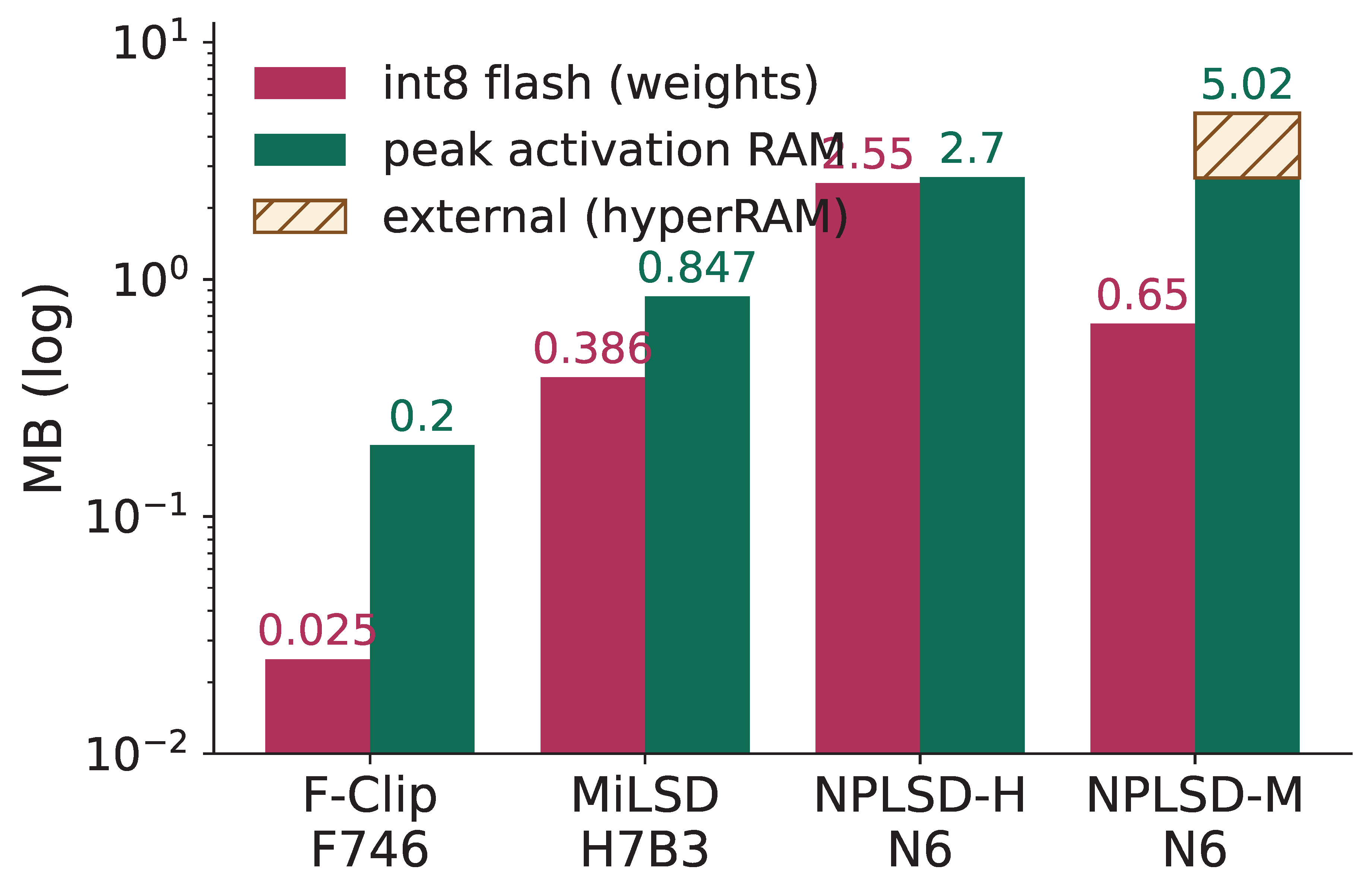
Every footprint and latency cell in Table 6 is now measured on-target across all five operating points, including the Jetson reference row. Figure 6 plots the accuracy-cost frontier. Figure 7 shows the flash and RAM footprint of each operating point, and Figure 5 details where the N6 activations reside: the int8 NPLSD-H arena fits entirely in internal SRAM, while its float fallback and the int8 NPLSD-M spill to external hyperRAM.
6.1. A Level-by-Level Selection Strategy
A selection rule falls out of the frontier. The board family fixes the detector class; within a class, the binding application constraint fixes the variant. Entry parts of a few hundred kilobytes admit only F-Clip-25k, which recovers coarse scene structure and nothing finer. Megabyte-class parts split by memory layout rather than by clock: those exposing one contiguous region carry MiLSD fully on-chip, while fragmented parts of the same nominal capacity cannot place it at all and should be passed over regardless of frequency.
Where an NPU is integrated, the choice narrows to a pair. A latency target or a hard on-chip requirement selects NPLSD-H, an accuracy target or a tight flash budget NPLSD-M. Once an edge-GPU module is admissible the lower-level constraints vanish altogether and the strongest published detectors run as released, at two orders of magnitude more energy per inference. Table 6 and Table 7 carry the measured values behind each of these choices, and the FOLD tier map in Figure 4 shows the result.
Figure 4.
The FOLD tier map. Each device class carries the strongest detector its memory and compute admit: F-Clip-25k on the 320 KB F746, MiLSD on the contiguous-SRAM H7B3, the two NPU-native NPLSD variants on the N6, and LINEA-N on the Jetson Xavier NX reference tier. All latencies and accuracies are measured on the deployed configurations.
Figure 4.
The FOLD tier map. Each device class carries the strongest detector its memory and compute admit: F-Clip-25k on the 320 KB F746, MiLSD on the contiguous-SRAM H7B3, the two NPU-native NPLSD variants on the N6, and LINEA-N on the Jetson Xavier NX reference tier. All latencies and accuracies are measured on the deployed configurations.
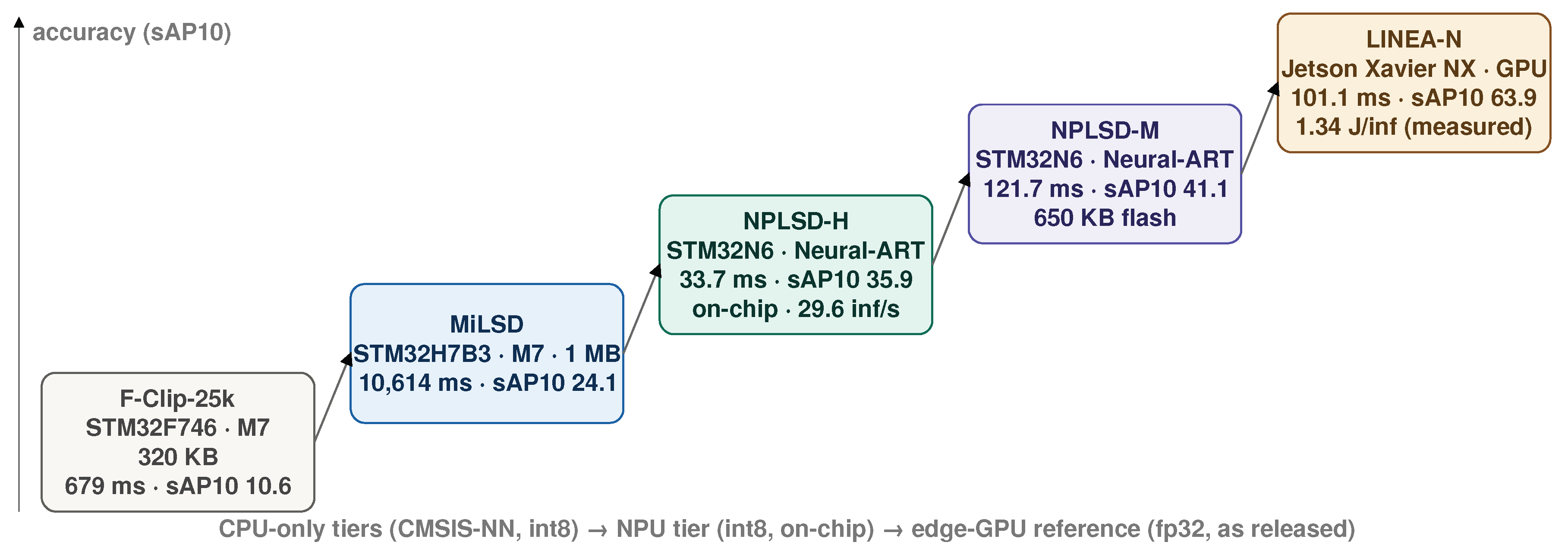
Figure 5.
Activation placement on the STM32N6. Float graphs overflow internal SRAM; int8 NPLSD-H fits entirely on-chip ( MB), while int8 NPLSD-M spills MB to hyperRAM. Residency, not capacity, separates the ms and ms points.
Figure 5.
Activation placement on the STM32N6. Float graphs overflow internal SRAM; int8 NPLSD-H fits entirely on-chip ( MB), while int8 NPLSD-M spills MB to hyperRAM. Residency, not capacity, separates the ms and ms points.
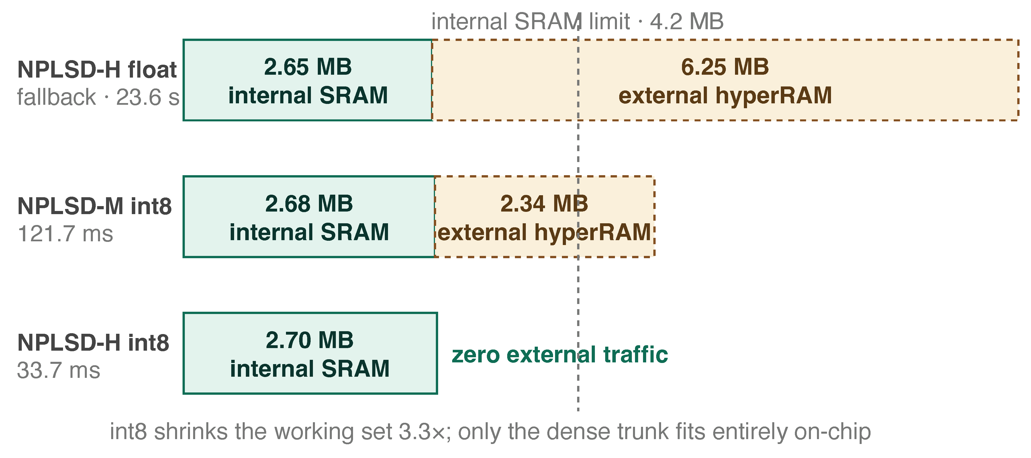
Figure 6.
Accuracy versus measured latency for the five deployed points (circles: STM32 in red, Jetson in amber). Accuracy rises as latency falls across device tiers. The two N6 points expose the trunk trade-off, and LINEA-N shows what an edge GPU buys in accuracy and energy (Table 6).
Figure 6.
Accuracy versus measured latency for the five deployed points (circles: STM32 in red, Jetson in amber). Accuracy rises as latency falls across device tiers. The two N6 points expose the trunk trade-off, and LINEA-N shows what an edge GPU buys in accuracy and energy (Table 6).
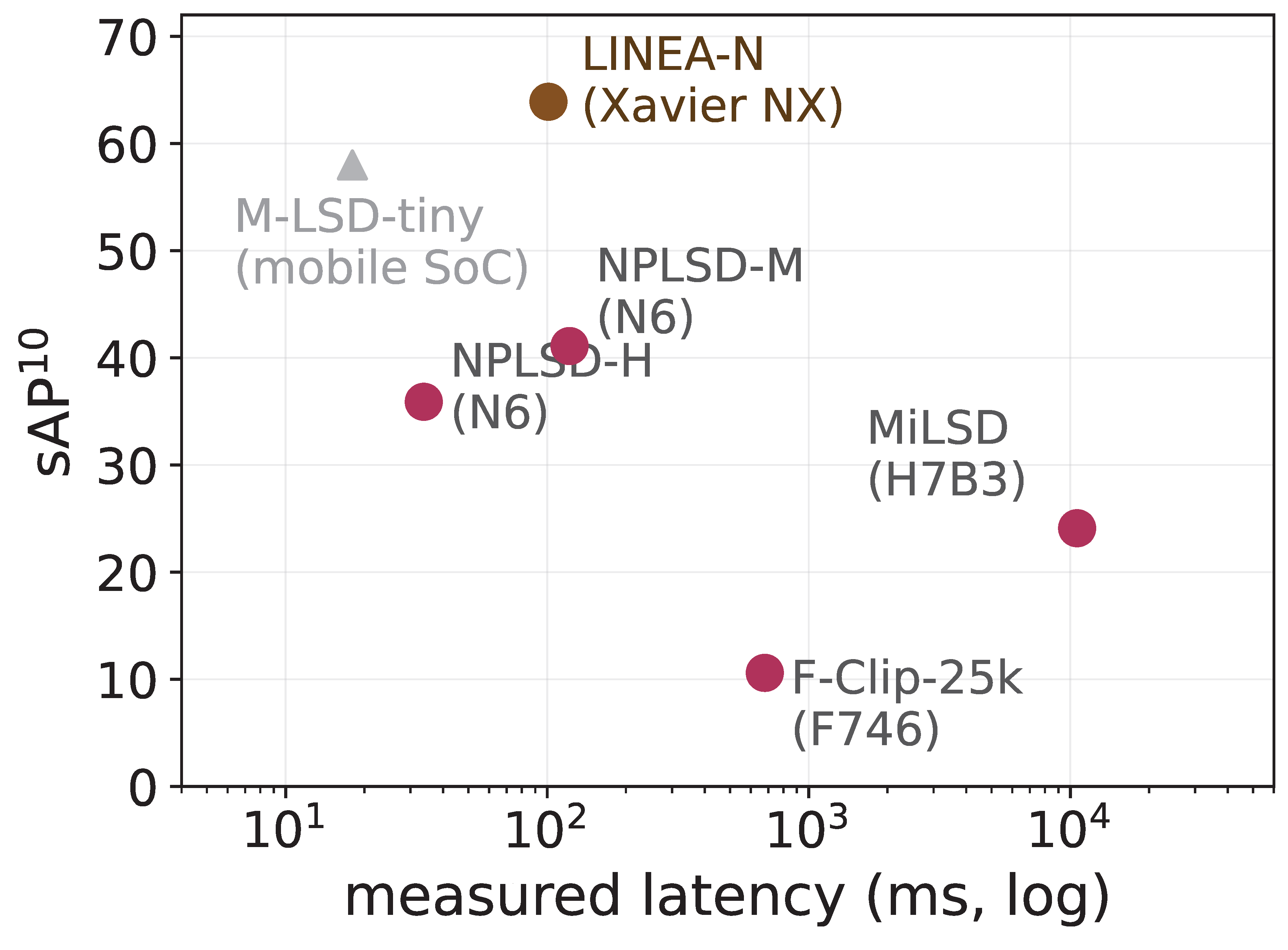
Figure 7.
Measured int8 flash (weights) and peak activation RAM per operating point (log scale). NPLSD-H runs from MB of flash with a MB arena held entirely in internal SRAM; NPLSD-M needs only MB of flash but spills MB of its MB arena to external hyperRAM (hatched).
Figure 7.
Measured int8 flash (weights) and peak activation RAM per operating point (log scale). NPLSD-H runs from MB of flash with a MB arena held entirely in internal SRAM; NPLSD-M needs only MB of flash but spills MB of its MB arena to external hyperRAM (hatched).
7. Discussion and Limitations
The three findings of this study share a shape worth stating plainly: on both device classes, what decides the outcome is where data sits and in what format, not how large the model is. On the no-NPU class, two otherwise comparable MB parts differ entirely in deployability because one exposes its memory as a single contiguous region and the other does not; capacity is the number on the datasheet, contiguity is the number that matters. On the NPU class, precision plays the same gatekeeping role: an integer accelerator cannot execute float convolutions, so a float graph falls back to the host core almost in full, and the same graph in int8 engages the array. Size, meanwhile, predicts little. The smaller variant is the slower one, because depthwise convolutions offer the MAC array little arithmetic intensity per byte moved and their activations spill off-chip. Choosing a trunk for an NPU is a placement and residency question before it is a parameter-count question.
Measuring the Jetson sharpens this picture rather than diminishing it. A commodity edge GPU lifts accuracy well beyond any microcontroller point with no co-design effort at all, yet each of its inferences spends about as much energy as a full MiLSD run on the H7B3. Where the power budget is milliwatt-class, the NPU tier is not an approximation of the GPU tier; it is the only option.
Several limitations should be acknowledged. The s inference time of MiLSD on a no-NPU Cortex-M7 is far from real-time for this workload. Energy figures are estimated rather than measured directly, with the Jetson tier as the exception: its power is read from the on-module sensor. Accuracy figures are inherited from off-device evaluation. On-target confirmation is limited to numerical agreement with the reference graphs.
8. Conclusion
This paper has presented FOLD, a free and reproducible framework for deploying line-segment detectors on STM32 microcontrollers. FOLD was demonstrated end-to-end at four operating points: a 25k-parameter F-Clip baseline on a KB STM32F746, MiLSD on a MHz STM32H7B3 (both fully on-chip with no accelerator), and the NPU-native NPLSD pair on an STM32N6 whose operators map onto the Neural-ART accelerator. A fifth, reference deployment measures LINEA-N on a Jetson Xavier NX and closes the map from above.
Across these points, the int8 flash footprint ranges from KB to MB. Accuracy rises from to on the STM32 tiers, and to on the GPU reference, and the N6 tier reaches inferences per second. Three key findings have been established. First, the same MiLSD model cannot be placed on the faster but memory-fragmented STM32H743. On-chip deployability is therefore determined by SRAM layout, not size. Second, transformer detectors do not benefit from a convolutional NPU. This is why the NPU points are co-designed convolutional detectors, and why the transformer is measured on the GPU tier instead. Third, int8 quantization is the switch that engages the accelerator. Once engaged, dense trunks buy speed and on-chip residency, while depthwise trunks buy accuracy per byte of flash.
References
- Pumarola, A.; Vakhitov, A.; Agudo, A.; Sanfeliu, A.; Moreno-Noguer, F. PL-SLAM: Real-Time Monocular Visual SLAM with Points and Lines. In Proceedings of the IEEE Int. Conf. on Robotics and Automation (ICRA), 2017, pp. 4503–4508. [CrossRef]
- He, J.; Li, M.; Wang, Y.; Wang, H. PLE-SLAM: A Visual-Inertial SLAM Based on Point-Line Features and Efficient IMU Initialization, 2024, [arXiv:cs.RO/2401.01081]. Point-line features improve SLAM in low-texture/indoor scenes.
- Zhou, Y.; Qi, H.; Ma, Y. End-to-End Wireframe Parsing. In Proceedings of the IEEE/CVF Int. Conf. on Computer Vision (ICCV), 2019. L-CNN. arXiv:1905.03246.
- Xue, N.; Wu, T.; Bai, S.; Wang, F.D.; Xia, G.S.; Zhang, L.; Torr, P.H. Holistically-Attracted Wireframe Parsing. In Proceedings of the IEEE/CVF Conf. on Computer Vision and Pattern Recognition (CVPR), 2020. HAWP. arXiv:2003.01663.
- Dai, X.; Gong, H.; Wu, S.; Yuan, X.; Ma, Y. Fully Convolutional Line Parsing. Neurocomputing 2022, 506, 1–11. F-Clip. arXiv:2104.11207, . [CrossRef]
- Gu, G.; Ko, B.; Go, S.; Lee, S.H.; Lee, J.; Shin, M. Towards Light-weight and Real-time Line Segment Detection. In Proceedings of the AAAI Conf. on Artificial Intelligence, 2022. M-LSD / M-LSD-tiny; MobileNetV2, center+displacement. arXiv:2106.00186.
- Hassani Shariat Panahi, P.; Jalilvand, A.H.; Najafi, M.H. MiLSD: Micro Line-Segment Detector. arXiv:2607.06600, 2026. Companion work; same center/length/angle representation on a no-NPU Cortex-M7.
- Lai, L.; Suda, N.; Chandra, V. CMSIS-NN: Efficient Neural Network Kernels for Arm Cortex-M CPUs. arXiv preprint arXiv:1801.06601 2018.
- STMicroelectronics. STM32N6 Series: Arm Cortex-M55 Microcontrollers with Neural-ART Accelerator. https://www.st.com/en/microcontrollers-microprocessors/stm32n6-series.html, 2025. Neural-ART neural processing unit; on-chip SRAM ∼4.2 MB; external xSPI flash and hyperRAM.
- Xue, N.; Wu, T.; Bai, S.; Wang, F.D.; Xia, G.S.; Zhang, L.; Torr, P.H. Holistically-Attracted Wireframe Parsing: From Supervised to Self-Supervised Learning. IEEE Trans. on Pattern Analysis and Machine Intelligence (TPAMI) 2023. HAWPv2/v3. arXiv:2210.12971.
- Xu, Y.; Xu, W.; Cheung, D.; Tu, Z. Line Segment Detection Using Transformers without Edges. In Proceedings of the IEEE/CVF Conf. on Computer Vision and Pattern Recognition (CVPR), 2021. LETR. arXiv:2101.01909.
- Janampa, S.; Pattichis, M. DT-LSD: Deformable Transformer-Based Line Segment Detection. In Proceedings of the Proceedings of the Winter Conference on Applications of Computer Vision (WACV), February 2025, pp. 3477–3486.
- Janampa, S.; Pattichis, M. LINEA: Fast and Accurate Line Detection Using Scalable Transformers, 2025, [arXiv:cs.CV/2505.16264].
- Hu, S.; Zhao, L.; Wang, Q. EM-LSD: A lightweight and efficient model for multi-scale line segment detection. Robotics and Autonomous Systems 2026, 195, 105192. [CrossRef]
- Hassani Shariat Panahi, P.; Jalilvand, A.H.; Najafi, M.H. NPLSD: Accelerating Line-Segment Detection on NPU Microcontrollers. Preprints, 2026. Preprint, posted 26 August 2026, . [CrossRef]
- Lin, J.; Chen, W.M.; Cai, H.; Gan, C.; Han, S. MCUNetV2: Memory-Efficient Patch-based Inference for Tiny Deep Learning. In Proceedings of the Advances in Neural Information Processing Systems (NeurIPS), 2021. arXiv:2110.15352.
- Banbury, C.; Zhou, C.; Fedorov, I.; Matas Navarro, R.; Thakker, U.; Gope, D.; Janapa Reddi, V.; Mattina, M.; Whatmough, P.N. MicroNets: Neural Network Architectures for Deploying TinyML Applications on Commodity Microcontrollers. Proc. of Machine Learning and Systems (MLSys) 2021. arXiv:2010.11267.
- Jacob, B.; Kligys, S.; Chen, B.; Zhu, M.; Tang, M.; Howard, A.; Adam, H.; Kalenichenko, D. Quantization and Training of Neural Networks for Efficient Integer-Arithmetic-Only Inference. In Proceedings of the IEEE/CVF Conf. on Computer Vision and Pattern Recognition (CVPR), 2018. arXiv:1712.05877.
- STMicroelectronics. ST Neural-ART Accelerator: Introduction. https://www.st.com/resource/en/product_presentation/st-neural-art-accelerator-introduction.pdf, 2025. Convolution-oriented NPU; epoch-controller execution model.
- Banbury, C.; Reddi, V.J.; Torelli, P.; Holleman, J.; Jeffries, N.; Kiraly, C.; Montino, P.; Kanter, D.; Ahmed, S.; Pau, D.; et al. MLPerf Tiny Benchmark. Proc. Neural Information Processing Systems (NeurIPS) Datasets and Benchmarks 2021. arXiv:2106.07597. Standardized MCU inference benchmarking.
- STMicroelectronics. STM32F746xx Arm Cortex-M7 Microcontroller Datasheet. https://www.st.com/en/microcontrollers-microprocessors/stm32f746ng.html. 320 KB SRAM, 1 MB flash, 216 MHz Cortex-M7.
- NVIDIA Corporation. Jetson Xavier NX Series Module Data Sheet. DS-10184-001, 2020. https://developer.nvidia.com/embedded/jetson-xavier-nx.
- STMicroelectronics. ST Edge AI Suite / X-CUBE-AI / ST Edge AI Developer Cloud. https://www.st.com/en/embedded-software/x-cube-ai.html, 2025. Model analysis, int8 code generation, and on-target benchmarking for STM32.
- Peng, Y.; Li, H.; Wu, P.; Zhang, Y.; Sun, X.; Wu, F. D-FINE: Redefine Regression Task in DETRs as Fine-grained Distribution Refinement, 2024, [arXiv:cs.CV/2410.13842]. Source of the HGNetv2-B0 backbone used by LINEA and adapted here.
- Zhao, Y.; Lv, W.; Xu, S.; Wei, J.; Wang, G.; Dang, Q.; Liu, Y.; Chen, J. DETRs Beat YOLOs on Real-time Object Detection. In Proceedings of the IEEE/CVF Conf. on Computer Vision and Pattern Recognition (CVPR), 2024. RT-DETR. arXiv:2304.08069.
Figure 1.
MiLSD inference latency versus core clock across the STM32H7 family (measured). Latency follows the ideal trend. The 480 MHz H743 is absent because its fragmented SRAM cannot accommodate the model (Table 2).
Figure 1.
MiLSD inference latency versus core clock across the STM32H7 family (measured). Latency follows the ideal trend. The 480 MHz H743 is absent because its fragmented SRAM cannot accommodate the model (Table 2).
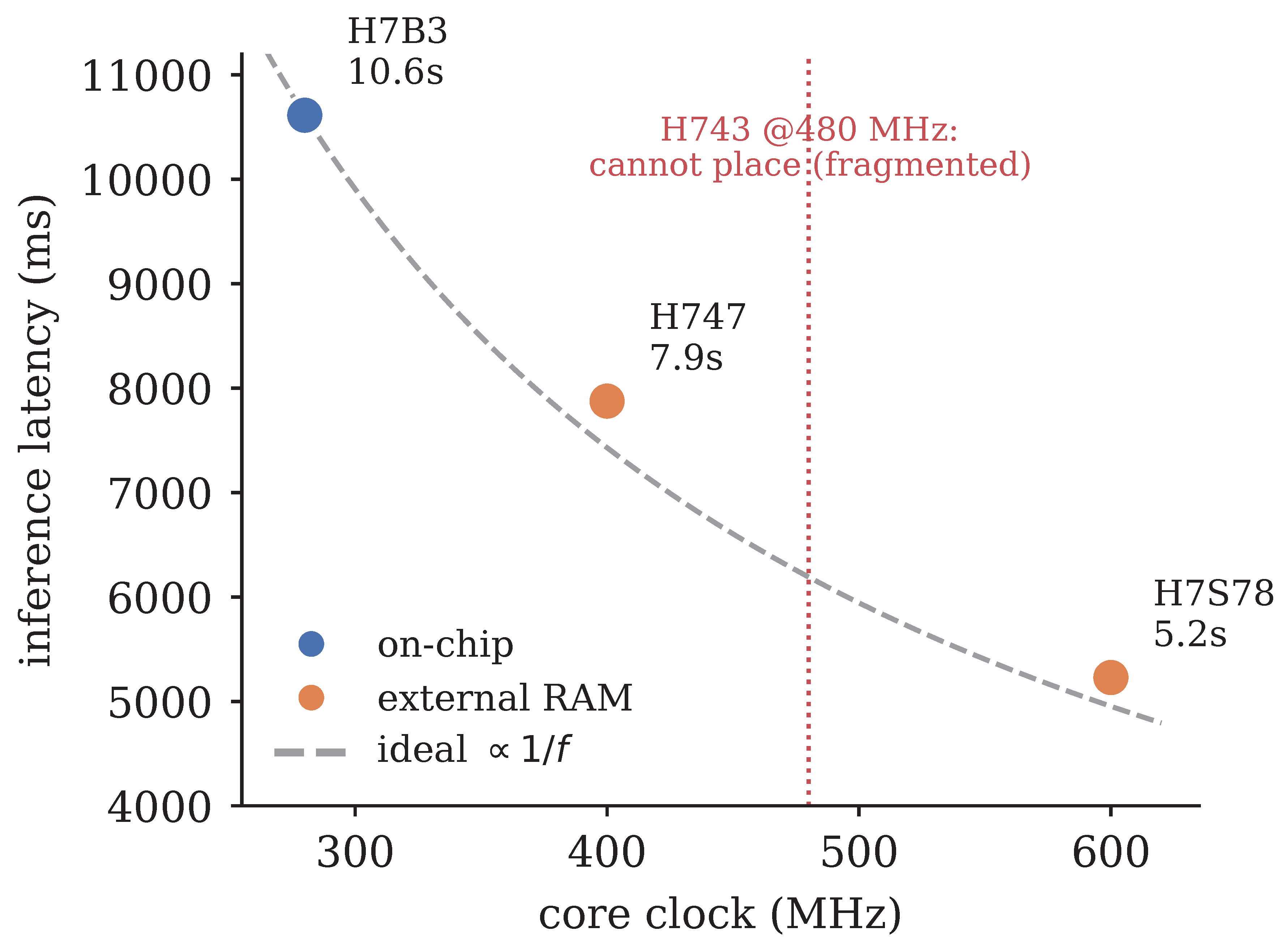
Figure 2.
Compiled epoch mapping on the STM32N6 for both NPLSD variants. Float graphs fall back to software; int8 graphs contain zero software epochs. Precision, not graph structure, decides accelerator utilization.
Figure 2.
Compiled epoch mapping on the STM32N6 for both NPLSD variants. Float graphs fall back to software; int8 graphs contain zero software epochs. Precision, not graph structure, decides accelerator utilization.
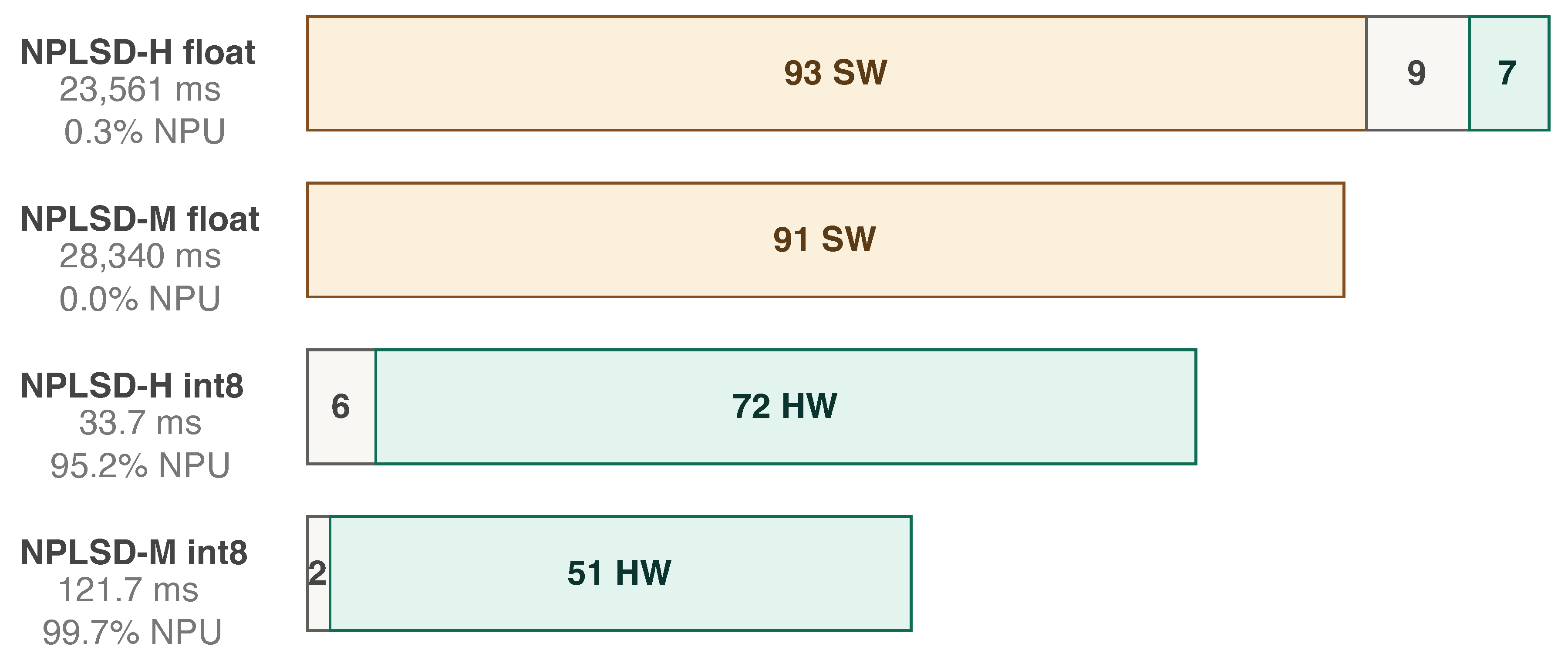
Table 3.
Per-layer cost of MiLSD on the STM32H7B3 (int8, pixel input). Latency is measured. Per-layer MACC values are analytic and sum to the tool’s reported G.
Table 3.
Per-layer cost of MiLSD on the STM32H7B3 (int8, pixel input). Latency is measured. Per-layer MACC values are analytic and sum to the tool’s reported G.
| Layer (output) | Wt. (KiB) | MACC (M) | Lat. (ms) | % |
|---|---|---|---|---|
| conv0 () | 0.3 | 4.7 | 69.4 | 0.7 |
| conv1 () | 18.0 | 75.5 | 338.9 | 3.2 |
| conv2 () | 72.0 | 302.0 | 1672.6 | 15.8 |
| conv3 () | 144.0 | 604.0 | 4177.8 | 39.4 |
| conv4 () | 144.0 | 604.0 | 4178.1 | 39.4 |
| reduce (32, ) | 4.0 | 16.8 | 65.6 | 0.6 |
| resize () | — | — | 4.7 | 0.0 |
| head () | 1.1 | 18.9 | 101.9 | 1.0 |
| transpose | — | — | 5.5 | 0.1 |
| total | 383 | 1626 | 10 614 | 100 |
Table 4.
Operator support across deployment targets. HW denotes an accelerator epoch; SW executes on the Cortex-M core.
Table 4.
Operator support across deployment targets. HW denotes an accelerator epoch; SW executes on the Cortex-M core.
| Operator | H7 CPU (CMSIS-NN) | N6 NPU, int8 | N6 NPU, float |
|---|---|---|---|
| Conv (dense / ) | SW | HW | SW fallback |
| Conv (depthwise) | SW | HW (low util.) | SW fallback |
| ReLU / ReLU6 (Clip) | SW | HW | SW fallback |
| Add · Concat · MaxPool | SW | HW | SW fallback |
| Resize (nearest) | SW | HW | SW fallback |
| Resize (bilinear, align corners) | SW | no primitive | no primitive |
| Pad (asymmetric) | SW | fold into Conv | fold into Conv |
| Softmax / Attention | SW | SW fallback | SW fallback |
| GridSample (deformable) | SW | SW fallback | SW fallback |
| LayerNorm · TopK · Gather | SW | SW fallback | SW fallback |
Disclaimer/Publisher’s Note: The statements, opinions and data contained in all publications are solely those of the individual author(s) and contributor(s) and not of MDPI and/or the editor(s). MDPI and/or the editor(s) disclaim responsibility for any injury to people or property resulting from any ideas, methods, instructions or products referred to in the content. |
© 2026 by the authors. Licensee MDPI, Basel, Switzerland. This article is an open access article distributed under the terms and conditions of the Creative Commons Attribution (CC BY) license (http://creativecommons.org/licenses/by/4.0/).
Copyright: This open access article is published under a Creative Commons CC BY 4.0 license, which permit the free download, distribution, and reuse, provided that the author and preprint are cited in any reuse.