

Submitted:
24 August 2026
Posted:
27 August 2026
You are already at the latest version
Abstract
TiO₂ nanotubes and ZnO thin films were investigated as oxide-based memristive systems for resistive switching and state-retention applications under variable environmental conditions. TiO₂ nanotubes were synthesized by electrochemical anodization, while ZnO thin films were deposited on Ti substrates by DC magnetron sputtering. Structural, chemical, and morphological properties were examined by Raman spectroscopy, X-ray diffraction, X-ray photoelectron spectroscopy, and scanning electron microscopy. TiO₂ exhibited a vertically aligned nanotubular morphology, whereas ZnO showed a granular thin-film surface. Electrical characterization was performed using Au top electrodes and Ti as the bottom electrode under atmospheric pressure and high-vacuum conditions, with temperature varied from 353 K down to 77 K. Both materials exhibited hysteretic current–voltage behavior associated with resistive switching, although their response was strongly influenced by morphology, defect distribution, and environmental conditions. TiO₂ nanotubes showed stable high- and low-resistance states, with an ON/OFF ratio of approximately 4.65, indicating robust state retention. The observed behavior was attributed to oxygen-vacancy-mediated transport, filament stabilization, and interface effects. These results highlight the relevance of comparing TiO₂ and ZnO nanostructures for identifying oxide systems capable of maintaining resistive states under temperature and pressure variations, supporting their potential for low-power non-volatile memory applications.
Keywords:
resistive switching
; endurence performance
; state retention
1. Introduction
Since their conceptualization in 1971 by Leon Chua [1], memristors have been a subject of sustained interest in modern electronic materials research. However, the consolidation of their experimental realization required several decades: it was not until 2008 that a first system faithfully reproducing the hysteresis behavior in current–voltage curves of TiO2 thin films was developed [2]. Following the experimental confirmation of this technology’s feasibility, research on this class of electronic elements grew considerably, focusing primarily on new materials and applications. Among the most prominent candidates in this domain is ZnO, with direct application in information storage systems such as resistive random-access memories (RRAM) [3].
Within this framework, metal oxides occupy a central role, owing both to the reproducibility of their switching behaviors and to their accessible, low-cost fabrication techniques, positioning them as promising candidates for next-generation electronic devices, including energy-efficient memory storage and computing applications [4]. TiO2 is recognized for its high structural stability and for exhibiting a resistive switching (RS) mechanism frequently based on the formation of phases that act as highly efficient conductive filaments. ZnO, in turn, offers distinctive advantages in terms of optical transparency, biocompatibility, and morphological versatility, enabling its integration into flexible electronics and biomedical devices [5,6].
Understanding of the mechanisms governing resistive switching has advanced significantly, enabling the classification of RRAM devices according to the nature of their underlying interactions. Those in which metallic cation migration occurs through a thin solid electrolyte film are termed electrochemical metallization memories (ECM); those exhibiting stoichiometry changes induced by temperature variations driven by current flow are classified as thermochemical memories (TCM); and those based on oxides mediated by oxygen anion migration and cation valence changes are identified as valence change memories (VCM). These categories account for the switching behavior and conductive channel formation in the vast majority of devices currently under development [7,8].
In low-power applications, however, alternative mechanisms have been proposed, suggesting that charge transport arises from carrier redistribution driven by the presence of oxygen vacancies acting as impurity centers [9,10]. Furthermore, the growing demand for memristive materials has given rise to a new area of study concerning the optimization of information retention [11], the analysis of the influence of synthesis technique [5,12], energy consumption, and the effect of environmental factors such as humidity and oxygen presence [13,14]. Temperature, geometry, and resistivity play a critical role in resistive switching due to Joule heating effects within the conductive filament [15]. Although thermal effects have been explored in isolation, device behavior under variable pressure conditions — particularly in high-vacuum environments — remains an open area of investigation [16].
This work compares the switching behavior and resistive state retention of TiO2 and ZnO devices under variations of pressure and temperature. TiO2 samples were synthesized by electrochemical anodization, and ZnO thin films were deposited by DC magnetron sputtering. Structural characterization was performed by Raman spectroscopy and X-ray diffraction, while surface morphology was examined by scanning electron microscopy. Comparative electrical characterization was carried out through current–voltage (I–V) measurements at ambient pressure and under high vacuum at different temperature values. Robustness validations were conducted in both cases.
2. Materials and Methods
2.1. Synthesis of ZnO Thin Films
Ti substrates (99.99% purity) with 1.2 x 3.3 cm and 50 μm thickness were cleaning with Alconox, distilled water, deionized water, and drying them with gaseous N2. Thin films of ZnO (99.99% purity) were deposited by DC magnetron sputtering at a power of 100 W and a working pressure of 2.5 x 10⁻² Torr for 10 min. Electrical contacts using vacuum metal evaporation (PVD system) with aluminum masks were deposited. 0.150 g of Au was deposited at a working pressure of 3x10⁻⁵ Torr. For electrode deposition, the samples were annealing to 473K for 40 s, for stimulated the Au addition in the samples. The samples with contacts followed by annealing process at the same temperature for 2 hours to improve adhesion.
2.2. Synthesis of TiO2 Nanotubes
TiO2 nanotubes were fabricated by electrochemical anodization at room temperature. Two Ti foils were used, one as the cathode and the other as the anode, immersed in a solution of 0.25 wt% ammonium fluoride (NH4F), 2 wt% distilled water, and 97.75% ethylene glycol, with constant agitation of the 250 rpm. A square wave signal (alternating voltage) was applied, varying between 20 V for 5 min and 80 V for 1 min, with a total anodizing time of 12 min. Following the same contact deposition methodology, the electrode contacts were carried out.
2.3. Characterization Methods
Structural characteristics were analyzed using a Horiba Xplora Plus Raman microscope with laser interaction of 532 nm, in conjunction with a PANalytical Xpert Pro DY2690 X-ray diffractometer with a Cu-Ka source and 40 kV. Additionally, X-ray Photoelectron Spectroscopy (XPS) measurements were realized in an XPS/ISS surface characterization platform made by SPECS GmbH with Al-Ka X-ray source, operated at 200 W. Morphological properties were obtained using a Tescan Vega 3 scanning electron microscope (SEM). For environmental electrical behavior testing, the KeyFactor’s Probe Station environment module was used in vacuum ranges from 10−5 Torr and temperatures between 353 K and 77 K. I-V curves and robustness were evaluated with a Keithley Model 2460 6.5-digit resolution meter with copper wires (gauge) were soldered to the Au contacts using silver paste and then to a tin-plated circuit board prepared for electrical characterization measurements.
3. Results
Raman spectra of TiO2 nanotubes and ZnO thin films were present in the Figure 1. TiO2 has optical phonons at the Γ point where g represents Raman modes active, u IR modes active and E modes degenerate [17]. Figure 1a shows Raman shift associated to the anatase an ruile phases with band at 414 cm-1 and 602 cm-1, respectively. The peak shift of the both cases can be attributed to the amorphous contribution and defect in the structural to the TiO2 [18,19]. The peak shift in both cases can be attributed to the amorphous contribution and the structural defect of TiO2. This behavior is associated with the synthesis process, which has resulted in the production of amorphous nanotubes [18,19].
ZnO crystallizes in the hexagonal wurtzite structure, belonging to the space group P63mc. Group-theoretical analysis predicts the optical phonons at the Γ point as A1g + 2B1g + Eg + 2Eu, where A1 and Eg are both Raman- and infrared-active, Eu modes are Raman-active only, and B1 modes are silent [20,21]. The A1 and E1 modes are further split into TO and LO components, while the E modes are doubly degenerate. In the Figure 1b, the band at 579 cm−1 can be assigned to the longitudinal optical mode of ZnO, commonly associated with A1g(LO) [10,11]. In contrast, the bands at 252 and 674 cm−1 are not typical first-order Raman modes of ideal wurtzite ZnO and are more likely related to second-order scattering processes, disorder-induced modes, or defect-associated contributions [22].
Figure 2 shows XPS spectra of the samples with HR spectra of Ti, Zn and O identifications. The high-resolution Ti 2p XPS spectrum (see lower inset Figure 2a) exhibits two well-defined peaks located at binding energies of approximately 459 eV and 464.8 eV, corresponding to the Ti 2p3/2 and Ti 2p1/2 components, respectively [23]. The observed spin–orbit splitting of ~5.8 eV is consistent with the characteristic signature of Ti4+ in TiO2. The absence of additional features or shoulder peaks at lower binding energies indicates that titanium is predominantly in the Ti4+ oxidation state. The high-resolution O 1s spectrum exhibits a dominant peak centered at approximately 530.4 eV, which is attributed to lattice oxygen (O2−) bonded to Ti4+ in the TiO2 structure. A secondary component at higher binding energies (≈532.1 eV) is also observed, which is commonly associated with oxygen vacancies, surface hydroxyl groups, or defect-related oxygen species [24].
The high-resolution Zn 2p XPS spectrum exhibits two well-defined peaks centered at approximately 1019.4 eV and 1042.5 eV, corresponding to the Zn 2p3/2 and Zn 2p1/2 components, respectively. The observed spin–orbit splitting of about 23,1 eV is characteristic of Zn2+ species in ZnO [25]. This assignment is further supported by the Zn LMM Auger spectrum, whose line shape and kinetic energy position are consistent with oxidized zinc rather than metallic Zn. Taken together, the Zn 2p and Zn LMM results confirm that zinc is predominantly present in the Zn2+ oxidation state, as expected for ZnO [26].
Topographic properties of the samples were investigated by scanning electron microscopy (SEM), as shown in Figure 3. The TiO2 nanotubes (Figure 3a) exhibit a well-defined tubular morphology, vertically aligned and uniformly distributed over the substrate. The nanotubes present an average length of ~518.9 ± 15.57 nm, forming a highly ordered array with relatively homogeneous dimensions. The cross-sectional view confirms the formation of densely packed nanotube walls, which are expected to favor directional charge transport along the tube axis.
In contrast, the ZnO thin films deposited on titanium foil (Figure 3b) display a granular surface morphology, characterized by the presence of agglomerated grains and irregular clusters distributed across the surface. Additionally, the formation of scale-like features can be observed, which are associated with the underlying substrate and the growth dynamics of the film.
On the other hand, the electrical response of the TiO2 nanotube devices was evaluated under two different environmental conditions. First, measurements were carried out at room temperature and atmospheric pressure. Subsequently, the devices were characterized under high-vacuum conditions while varying the temperature from 353 K down to 77 K (Figure 4). The stability of the hysteretic I–V response and the evolution of the resistive states were investigated using TiO2 nanotubes with Au top electrodes (TE) and Ti foil as bottom electrodes (BE).
Figure 4a shows the I–V characteristics obtained under vacuum conditions while increasing temperature from room temperature up to 353 K. In all cases, the characteristic hysteresis behavior remains preserved, indicating that the resistive switching mechanism is maintained even under thermal variations. However, a progressive increase in current magnitude can be observed at elevated temperatures, particularly at 353 K. This behavior suggests an enhancement of charge transport processes due to thermally activated carrier mobility and increased oxygen vacancy dynamics. Under higher temperatures, the migration of ionic defects and local charge redistribution become energetically favored, facilitating conductive pathway formation and increasing the effective conductivity of the device.
In contrast, Figure 4b presents the I–V curves obtained at lower temperatures under high vacuum conditions. Despite cooling down to 77 K, the devices continue exhibiting clear hysteretic switching behavior, demonstrating remarkable stability of the memristive response. Nevertheless, a gradual reduction in current magnitude is observed as temperature decreases. Such behavior can be associated with reduced ionic mobility and suppressed defect migration at cryogenic temperatures, limiting conductive filament evolution. Despite these changes, the persistence of well-defined switching events indicates that the resistive states remain accessible even under strong thermal constraints.
Interestingly, the switching voltages exhibit only moderate variations over the explored temperature range, suggesting that the underlying transport mechanism possesses good thermal robustness. The preservation of the hysteretic response under both heating and cooling conditions indicates that the conductive channels formed within the TiO2 nanotubes remain sufficiently stable against external perturbations. These findings demonstrate that TiO2 nanotube devices exhibit reliable operation under extreme environmental conditions.
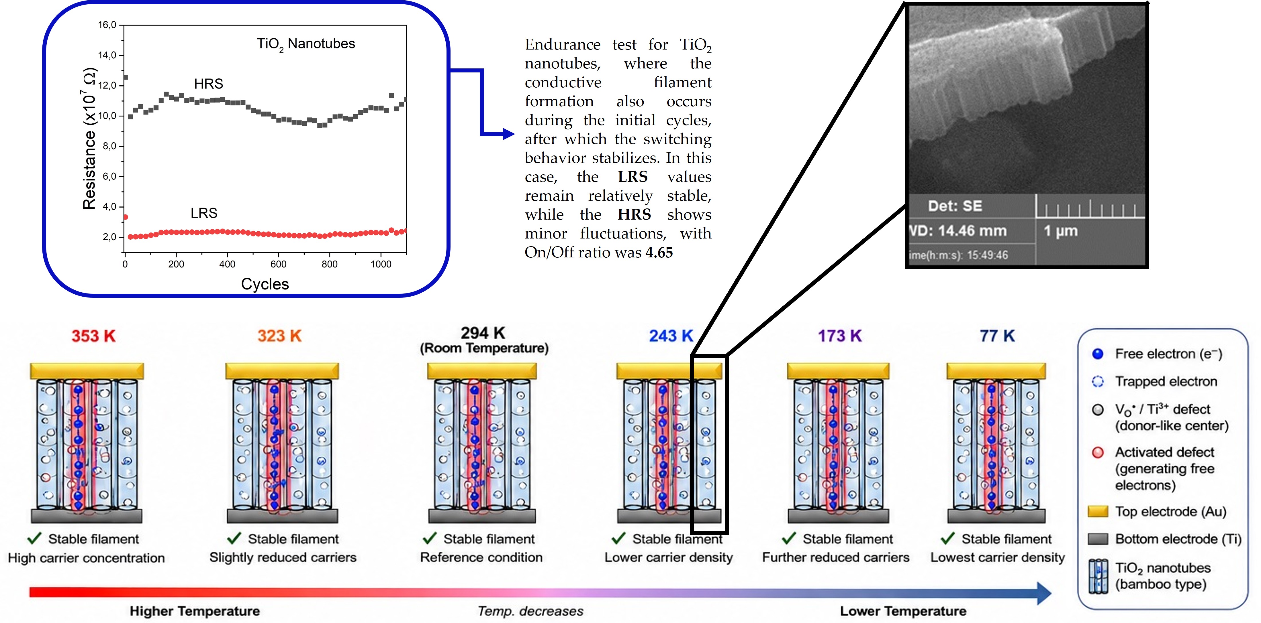
A similar trend is observed in the endurance test for TiO2 nanotubes (Figure 4b), where the conductive filament formation also occurs during the initial cycles, after which the switching behavior stabilizes. In this case, the LRS values remain relatively stable, while the HRS shows minor fluctuations, with On/Off ratio was 4.65 (see Figure 5).
Figure 5 presents the evolution of the high-resistance state (HRS) and low-resistance state (LRS) of the TiO2 nanotube device during 1100 consecutive switching cycles. A clear separation between both resistive states is maintained throughout the entire measurement, demonstrating the stability and reproducibility of the resistive switching process.
The HRS remains within the range of approximately (9.4–11.5) × 107 Ω, while the LRS fluctuates around (2.0–2.4) × 107 Ω. Although small cycle-to-cycle variations are observed in both states, no significant degradation or progressive convergence between HRS and LRS is detected. The fluctuations are attributed to minor local rearrangements of defect-related conductive pathways and variations in charge trapping and detrapping processes within the oxide matrix. The average resistance ratio between HRS and LRS remains close to 4.5–5 during the entire cycling test, confirming the robustness of the memory window. These results demonstrate that TiO2 nanotubes possess excellent endurance characteristics and stable state retention, which are desirable features for non-volatile memory applications operating under repetitive switching conditions.
In comparison, the ZnO thin films present the electrical response was in the same condition, varying the temperature between 373 K to 172 K, and pressure (Figure 6). Unlike TiO2 nanotubes, ZnO films exhibited a stronger dependence of the current magnitude on both temperature and pressure. Nevertheless, the hysteretic behavior remained observable throughout the explored temperature range, indicating the persistence of memory-related transport mechanisms.
Figure 6a shows the I–V characteristics measured under vacuum conditions at temperatures between 294 K and 373 K. A significant increase in current is observed when the temperature is increased from room temperature to 303 K, reaching the highest conductivity values within the explored range. This behavior suggests a thermally activated transport mechanism, where charge carrier mobility and defect-assisted conduction are enhanced at moderate temperatures. The presence of abrupt current transitions at specific voltages indicates discrete switching events, which may be associated with the activation of conductive pathways or charge trapping–detrapping processes within the ZnO matrix.
Figure 6b presents the I–V characteristics obtained at cryogenic temperatures under high-vacuum conditions. In contrast to the behavior observed in TiO2 nanotubes, the current decreases by approximately three orders of magnitude, from 10−4 A to 10−7 A, indicating a strong suppression of charge transport at low temperatures. Despite this reduction, the hysteretic response remains visible, demonstrating that the switching mechanism survives even when thermal activation processes are significantly reduced.
4. Discussion
The structural and spectroscopic analyses further suggest that defects play a fundamental role in the switching response. Raman measurements of TiO2 revealed the coexistence of anatase and rutile contributions accompanied by spectral shifts and broadening, indicating the presence of structural disorder and amorphous regions. Likewise, XPS analysis of the O 1s signal evidenced contributions associated with oxygen-deficient environments and defect-related oxygen species. Oxygen vacancies are widely recognized as dominant active centers in valence change memory systems [18,19], acting as nucleation sites for conductive filament formation and charge transport channels. Their redistribution under electrical stress may promote reversible changes in local conductivity and therefore stabilize resistive switching [19]. Similar oxygen-defect-mediated conduction processes have been extensively described in TiO2 and ZnO-based RRAM devices.
The electrical behavior observed in TiO2 nanotubes and ZnO thin films can be interpreted by considering differences in morphology, defect structure, and conductive mechanism established during synthesis. The SEM observations revealed that TiO2 develops an ordered nanotubular architecture, whereas ZnO exhibits a granular morphology composed of agglomerated surface features. Such structural differences are expected to strongly influence charge transport mechanisms and conductive filaments formation. In nanotubular systems, charge carriers may preferentially propagate along vertically aligned “channels” defined by the nanotube walls, promoting directional transport and localized defect accumulation. In comparison, the granular nature of ZnO thin films introduces a larger density of grain boundaries and interfacial discontinuities, where charge trapping and scattering processes may occur. Similar effects have been reported in oxide-based resistive memories, where geometry and microstructure significantly influence filament formation and switching reproducibility [18,27].
The differences observed in resistive switching stability can also be associated with distinct conductive channel dynamics in both systems. In TiO2 nanotubes, the tubular geometry may facilitate the formation of distributed conductive pathways along the nanotube walls rather than abrupt localized filament rupture. Such transport behavior can favor switching reproducibility and improve resistance-state retention during repeated cycling. The endurance results demonstrated that the separation between HRS and LRS remained preserved over extended operation, indicating stable conductive path evolution. Small resistance fluctuations observed during cycling may be attributed to stochastic oxygen vacancy redistribution and subtle modifications of filament geometry. Similar cycle-to-cycle variations have frequently been reported in oxide memristive systems without significantly affecting functionality.
Environmental conditions are also expected to affect the electrical response through defect-mediated transport mechanisms. Previous studies have demonstrated that pressure, oxygen concentration, and temperature directly influence charge transport and conductive filament stability in oxide materials. Under vacuum conditions, surface adsorbates and oxygen-related interactions may be suppressed, modifying vacancy populations and charge trapping processes. Additionally, temperature variations can alter ionic mobility and Joule-heating-assisted filament evolution. Therefore, the comparative study performed under atmospheric and vacuum conditions provides additional insight into the robustness of the switching process under external perturbations In the TiO2 nanotubes and ZnO thin films. Such behavior is particularly relevant for practical applications involving harsh environments, flexible electronics, and low-power non-volatile memory technologies.
The preservation of hysteresis under both heating and cooling conditions suggests that the observed switching is not solely governed by thermally activated conduction but also involves defect-mediated memory effects. Oxygen vacancies, grain-boundary states, and localized charge trapping centers are likely to contribute to the switching process. The strong temperature dependence of the current indicates that ZnO exhibits a larger activation energy for charge transport than TiO2 nanotubes, making its electrical response more sensitive to environmental conditions.
A notable difference between both oxide systems is the magnitude of the temperature dependence. While TiO2 nanotubes preserve similar current levels over the explored temperature range, ZnO films experience a pronounced reduction in conductivity at cryogenic temperatures. This behavior may be attributed to the different conduction pathways available in each material. The vertically aligned nanotubular architecture of TiO2 facilitates the formation of stable defect-mediated conductive channels, whereas charge transport in ZnO is more strongly influenced by grain boundaries, surface states, and thermally activated carriers. Consequently, TiO2 nanotubes exhibit greater robustness under extreme thermal conditions, whereas ZnO provides valuable insight into the role of temperature-dependent defect dynamics in oxide-based memristive systems.
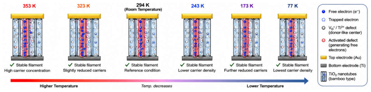
The electrical response observed in both TiO2 nanotubes and ZnO thin films can be interpreted in terms of defect-assisted electronic transport. In this scenario, the conductive filament is not formed by the long-range migration of oxygen ions but rather by the establishment of preferential electron percolation pathways through defect-rich regions distributed within the oxide matrix [19]. Oxygen vacancies, Ti3+ centers, and other structural defects act as donor-like states capable of releasing free electrons, thereby increasing the local carrier concentration and facilitating electronic conduction under an applied electric field (see Figure 7).
When a positive bias is applied, electrons injected from the electrodes preferentially occupy and connect neighboring defect states, progressively creating a continuous low-resistance conduction channel between both electrodes. The transition from the high-resistance state (HRS) to the low-resistance state (LRS) is therefore associated with the formation of an electronically connected defect network rather than with the physical growth of a metallic filament. During the RESET process, electron redistribution and trapping at defect sites partially disrupt this percolation pathway, restoring the high-resistance state while preserving the underlying defect structure.
The stability of the hysteretic response over a wide temperature range provides additional evidence supporting this mechanism. If the switching process were dominated by ionic migration, a significant suppression of the resistive switching behavior would be expected at cryogenic temperatures due to the drastic reduction of ionic mobility. However, both TiO2 nanotubes and ZnO thin films preserve well-defined hysteresis loops even down to low temperatures, indicating that charge transport remains governed by electronic processes. Although the current magnitude decreases as thermal activation is reduced, the persistence of the switching window demonstrates that the conductive pathways are sustained by defect-related electronic states that remain active under both vacuum and low-temperature conditions.
The different temperature dependence observed in TiO2 and ZnO can be attributed to their distinct microstructures. The vertically aligned nanotubular architecture of TiO2 provides quasi-one-dimensional conduction pathways along the nanotube walls, promoting the formation of stable defect-assisted electron channels. In contrast, ZnO thin films exhibit a granular morphology in which charge transport is additionally influenced by grain boundaries and surface states. Consequently, ZnO displays a stronger temperature dependence of the current magnitude, while TiO2 nanotubes exhibit greater robustness against thermal variations. Nevertheless, the preservation of hysteresis in both systems indicates that defect-mediated electronic conduction constitutes the dominant switching mechanism.
5. Conclusions
In this work, the electrical behavior of TiO2 nanotubes and ZnO thin films was studied investigated under variations of temperature and pressure in order to evaluate their potential as oxide-based memristive systems. Raman spectroscopy, X-ray photoelectron spectroscopy, and scanning electron microscopy confirmed the formation of defect-containing nanostructures with distinct morphologies, consisting of auto-aligned TiO2 nanotubes and granular ZnO thin films. Both materials exhibited stable hysteretic current–voltage characteristics associated with resistive switching behavior. The preservation of the switching response under high-vacuum conditions and over a wide temperature range demonstrated the robustness of the memory effect against environmental perturbations. TiO2 nanotubes showed superior stability of the resistive states, maintaining an ON/OFF ratio close to 4.65 during endurance measurements, while ZnO thin films exhibited a stronger dependence of the current magnitude on temperature. The combined structural, spectroscopic, and electrical results suggest that the switching mechanism can be predominantly governed by defect-assisted electronic transport. Oxygen vacancies and defect-related electronic states act as donor centers that generate free charge carriers, promoting the formation of conductive percolation pathways between the electrodes. The persistence of hysteresis even at cryogenic temperatures indicates that electronic transport processes play a dominant role over long-range ionic migration. The comparative analysis reveals that the nanotubular architecture of TiO2 provides greater thermal robustness than the granular ZnO morphology, favoring stable conductive pathways and improved retention of resistive states. These findings demonstrate the potential of both oxide nanostructures for non-volatile memory applications operating under demanding environmental conditions and provide further insight into the role of defect-mediated conduction in memristive devices.
Author Contributions
For research articles with several authors, a short paragraph specifying their individual contributions must be provided. The following statements should be used Conceptualization, Jorge A. Calderón, Heiddy P. Quiroz, and A. Dussan; methodology, Jorge A. Calderón, Heiddy P. Quiroz, and A. Dussan.; software, Cristian E. Patiño, Daniel E. Nuñez, Y. Porras Ramírez, Jorge A. Calderón, Heiddy P. Quiroz, A. Dussan; validation, Jorge A. Calderón, Heiddy P. Quiroz, and A. Dussan.; formal analysis, Jorge A. Calderón, Heiddy P. Quiroz, A. Dussan; investigation, Cristian E. Patiño, Daniel E. Nuñez, Y. Porras Ramírez, Jorge A. Calderón, Heiddy P. Quiroz, A. Dussan; resources, Cristian E. Patiño, Daniel E. Nuñez, Y. Porras Ramírez, Jorge A. Calderón, Heiddy P. Quiroz, A. Dussan; data curation, Cristian E. Patiño, Daniel E. Nuñez, Y. Porras Ramírez, Jorge A. Calderón, Heiddy P. Quiroz, A. Dussan; writing—original draft preparation, Cristian E. Patiño, Daniel E. Nuñez, Y. Porras Ramírez, Jorge A. Calderón, Heiddy P. Quiroz, A. Dussan; writing—review and editing, Jorge A. Calderón, Heiddy P. Quiroz, and A. Dussan; visualization, Cristian E. Patiño, Daniel E. Nuñez, Y. Porras Ramírez, Jorge A. Calderón, Heiddy P. Quiroz, A. Dussan; supervision, Jorge A. Calderón, Heiddy P. Quiroz, and A. Dussan; project administration, Jorge A. Calderón, Heiddy P. Quiroz, and A. Dussan; funding acquisition, Jorge A. Calderón, Heiddy P. Quiroz, and A. Dussan. All authors have read and agreed to the published version of the manuscript.
Funding
This research was funded by Universidad Nacional de Colombia through QUIPU 202010042199, and MinCiencias through Conv. 937.
Data Availability Statement
Data sets generated during the current study are available from the corresponding author on reasonable request.
Acknowledgments
The Universidad Nacional de Colombia supported this work via project QUIPU 202010042199, MinCiencias through Conv. 937. Special acknowledgment to Cluster in Convergent Sciences and Technologies of the Universidad Central for your support in this research.
Conflicts of Interest
The authors declare no conflicts of interest.
Abbreviations
The following abbreviations are used in this manuscript:
| XPS | X-ray Photoelectron Spectroscopy |
| SEM | Scanning Electron Microscopy |
| XRD | X-Ray Diffraction |
| TE | Top Electrode |
References
- Chua, L. Memristor-the missing circuit element. IEEE Trans. Circuit Theory 2003, 18(5), 507–519. [Google Scholar]
- Strukov, D. B.; Snider, G. S.; Stewart, D. R.; Williams, R. S. The missing memristor found. Nat. 2008, 453(7191), 80–83. [Google Scholar] [CrossRef] [PubMed]
- Nowak, E.; Chłopocka, E.; Szybowicz, M. ZnO and ZnO-based materials as active layer in resistive random-access memory (RRAM). Cryst. 2023, 13(3), 416. [Google Scholar] [CrossRef]
- Loizos, M.; Rogdakis, K.; Parambil, A. P.; Lira-Cantu, M.; Kymakis, E. Emerging materials for resistive switching memories: Prospects for enhanced sustainability and performance for targeted applications. APL Energy 2024, 2(4), 040901. [Google Scholar] [CrossRef]
- Illarionov, G. A.; Morozova, S. M.; Chrishtop, V. V.; Einarsrud, M. A.; Morozov, M. I. Memristive TiO2: Synthesis, Technologies, and Applications. Front. Chem. 2020, 8, 724. [Google Scholar] [CrossRef] [PubMed]
- Bulja, S.; Kopf, R.; Tate, A.; Cappuzzo, M.; Kozlov, D.; Claussen, H.; Wiegner, D.; Templ, W.; Mirshekar-Syahkal, D. High frequency resistive switching behavior of amorphous TiO2 and NiO. Sci. Rep. 2022, 12(1), 13804. [Google Scholar] [CrossRef] [PubMed]
- Munjal, S.; Khare, N. Valence change bipolar resistive switching accompanied with magnetization switching in CoFe2O4 thin film. Sci. Rep. 2017, 7(1), 12427. [Google Scholar] [CrossRef] [PubMed]
- Mejri, H.; Omri, K.; Ghiloufi, I.; Silva, J. P. B.; Gomes, M. J. M.; El Mir, L. Resistive switching behavior in ZnO: Ca thin films deposited by a pulsed laser deposition technique. Appl. Phys. A 2023, 129(3), 210. [Google Scholar] [CrossRef]
- Quiroz, Heiddy P.; Calderón, Jorge A.; Dussan, A. Magnetic switching control in Co/TiO2 bilayer and TiO2:Co thin films for magnetic-resistive random access memories (M-RRAM). J. Alloys Compd. 2020, 840, 155674. [Google Scholar] [CrossRef]
- Coey, J. M. D.; Venkatesan, M.; Fitzgerald, C. B. Donor impurity band exchange in dilute ferromagnetic oxides. Nat. Mater. 2005, 4(2), 173–179. [Google Scholar] [CrossRef] [PubMed]
- Melo, A.H.N.; Macêdo, M.A. Permanent Data Storage in ZnO Thin Films by Filamentary Resistive Switching. PLoS ONE 2016, 11(12), e0168515. [Google Scholar] [CrossRef] [PubMed]
- Quiroz, Heiddy P.; Terán, Cristian L.; Calderón, Jorge A.; Dussan, A. Tuning resistive switching in ZnO and TiO2 nanostructures with cobalt doping. J. Mater. Sci. Mater. Electron. 2025, 36(7), 1–12. [Google Scholar] [CrossRef]
- Lu, Wanheng; Wong, Lai-Mun; Wang, Shijie; Zeng, Kaiyang. Effects of oxygen and moisture on the I-V characteristics of TiO2 thin films. J. Mater. 2018, 4(3), 228–237. [Google Scholar] [CrossRef]
- Milano, G.; Luebben, M.; Laurenti, M.; Boarino, L.; Ricciardi, C.; Valov, I. Structure-Dependent Influence of Moisture on Resistive Switching Behavior of ZnO Thin Films. Adv. Mater. Interfaces 2021, 8, 2100915. [Google Scholar] [CrossRef]
- Dongale, T. D.; et al. Investigating the Temperature Effects on ZnO, TiO2, WO3 and HfO2 Based Resistive Random Access Memory (RRAM) Devices. J. Nano-Electron. Phys. 2016, 8(4), 04030. [Google Scholar] [CrossRef]
- Aldana, S.; Zhang, H. Unravelling the data retention mechanisms under thermal stress on 2D memristors. ACS Omega 2023, 8(30), 27543–27552. [Google Scholar] [CrossRef] [PubMed]
- Lukačević, Igor; Gupta, Sanjeev K.; Jha, Prafulla K.; Kirin, Davor. Lattice dynamics and Raman spectrum of rutile TiO2: The role of soft phonon modes in pressure induced phase transition. Mater. Chem. Phys. 2012, 137, 282–289. [Google Scholar] [CrossRef]
- Quiroz, Heiddy P.; Calderón, Jorge A.; Porras Ramírez, Y.; Dussan, A. TiO2 and TiO2:Co nanostructures for enhanced non-volatile memory: Insights into surface modification. Ceram. Int. 2025, 51, 38199–38211. [Google Scholar] [CrossRef]
- Quiroz, Heiddy P.; Serrano, J.E.; Dussan, A. Magnetic behavior and conductive wall switching in TiO2 and TiO2:Co self-organized nanotube arrays. J. Alloy. Compd. 2020, 825, 154006. [Google Scholar] [CrossRef]
- Hadžić, Branka. Raman study of surface optical phonons in ZnO(Co) nanoparticles prepared by hydrothermal method. Hem. Ind. 2013, 67(4), 695–701. [Google Scholar] [CrossRef]
- Korepanov, Vitaly I.; Chan, Si-Yuan; Hsu, Hsu-Cheng; Hamaguchi, Hiro-o. Phonon confinement and size effect in Raman spectra of ZnO nanoparticles. Heliyon 2019, 5, e01222. [Google Scholar] [CrossRef] [PubMed]
- Fischer, Dieter; Bloos, Dominik; Krajewska, Aleksandra; McNally, Graham M.; Zagorac, Dejan; Schön, Johann Christian. Raman Characterization of Dioxygen Species as Defects in Single-Crystal ZnO Including Their Pressure Dependence. Crystals 2025, 15, 574. [Google Scholar] [CrossRef]
- Vitanov, P.; Stefanov, P.; Harizanova, A.; Ivanova, T. XPS characterization of thin (Al2O3)x(TiO2)1-x films deposited on silicon. J. Phys. Conf. Ser. 2008, 113, 012036. [Google Scholar] [CrossRef]
- Wang, Jiayue; Mueller, David N.; Crumlin, Ethan J. Recommended strategies for quantifying oxygen vacancies with X-ray photoelectron spectroscopy. J. Eur. Ceram. Soc. 2024, 44(15), 116709. [Google Scholar] [CrossRef]
- Choa, Ha Eun; Kim, Min Young; Park, Chul Oh; et al. Mechanistic understanding of gas sensing in palladium nanoparticles-decorated porous ZnO nanosheets: Correlating energy barrier and ionized oxygen species with sensing performance. Sens. Actuators Rep. 2026, 11, 100422. [Google Scholar] [CrossRef]
- Henderson, Jeffrey D.; Buchanan, Sage D.C.; Grey, Lauren H.; et al. Zinc and cadmium: XPS chemical state determination and auger peak curve-fitting procedures. Appl. Surf. Sci. 2026, 730, 166284. [Google Scholar] [CrossRef]
- Ozga, Monika; Mroczynski, Robert; Matus, Krzysztof; Arabasz, Sebastian; Witkowski, Bartłomiej S. Filamentary Resistive Switching Mechanism in CuO Thin Film-Based Memristor. Materials 2025, 18, 3820. [Google Scholar] [CrossRef] [PubMed]
Figure 1.
Raman spectra of (a) TiO2 nanotubes, and (b) ZnO thin films on Ti substrate.
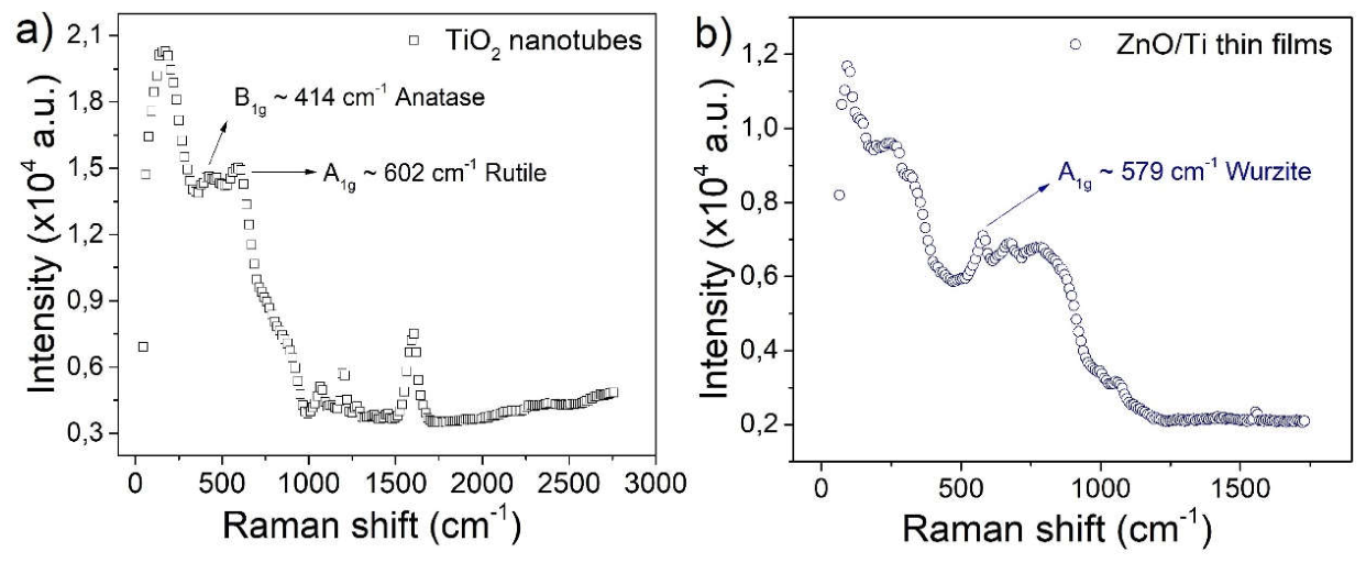
Figure 2.
HR-XPS spectra of (a) TiO2 nanotubes, and (b) ZnO thin films.
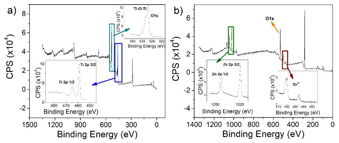
Figure 3.
SEM micrographs of (a) TiO2 nanotubes, and (b) ZnO thin films.
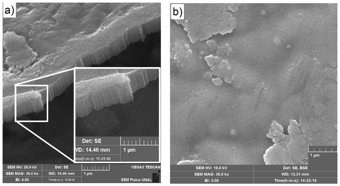
Figure 4.
I-V curves of TiO2 nanotubes varying with (a) high temperature, and (b) low temperature.
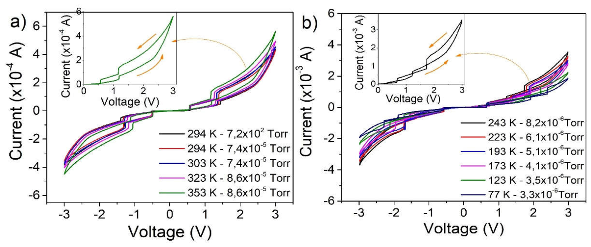
Figure 5.
Endurance performance of TiO2 nanotubes for 1200 cycles.
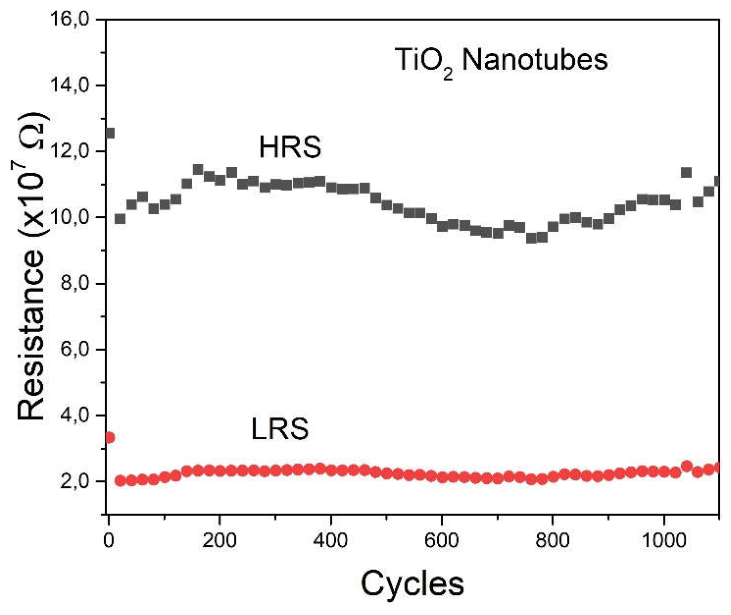
Figure 6.
I-V curves of ZnO thin film varying with (a) high temperature, and (b) low temperature.
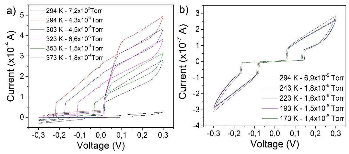
Figure 7.
Conductive filament stability under temperature in high vacuum condiction.
Disclaimer/Publisher’s Note: The statements, opinions and data contained in all publications are solely those of the individual author(s) and contributor(s) and not of MDPI and/or the editor(s). MDPI and/or the editor(s) disclaim responsibility for any injury to people or property resulting from any ideas, methods, instructions or products referred to in the content. |
© 2026 by the authors. Licensee MDPI, Basel, Switzerland. This article is an open access article distributed under the terms and conditions of the Creative Commons Attribution (CC BY) license (http://creativecommons.org/licenses/by/4.0/).
Copyright: This open access article is published under a Creative Commons CC BY 4.0 license, which permit the free download, distribution, and reuse, provided that the author and preprint are cited in any reuse.