

Submitted:
22 August 2026
Posted:
24 August 2026
You are already at the latest version
Abstract
Whether the plasticity of silicon at high temperatures originates from dislocation slip or solid-state phase transition remains difficult to investigate directly through experimental observation due to its microscopic nature. Using molecular dynamics simulations, we investigated the deformation behavior of silicon crystals along four typical crystallographic directions at a reduced temperature of T/Tm = 0.88. The results indicate that prior to yielding, compressive stress induces uniform amorphization throughout the crystal. Once the critical stress is exceeded, Shockley partial dislocations nucleate on the {111} crystal planes, initiating plastic flow, while the amorphous phase undergoes recrystallization during the stress relaxation. These findings demonstrate that at high temperatures, the plasticity of silicon involves both stress-assisted amorphization and dislocation-mediated plasticity, which occur sequentially rather than competing with one another. This study provides atomic-scale guidance for suppressing dislocation defects in the directional solidification growth of polycrystalline silicon.
Keywords:
silicon
; amorphization
; molecular dynamics
; mechanical properties
; dislocations
1. Introduction
Multicrystalline silicon (mc-Si) solar cells combine relatively low production cost with competitive conversion efficiency, and they remain a mainstay of the photovoltaic industry. Their efficiency, however, is still inferior to that of monocrystalline cells. The efficiency deficit stems primarily from crystal defects, such as grain boundaries, twins, dislocations, and impurities, introduced during casting. Among these, dislocations are the most detrimental to device performance [1,2,3,4,5]. Because dislocations multiply most readily while the ingot is still hot, understanding how silicon deforms near its melting point is essential for inhibiting dislocation generation during directional solidification. Silicon also offers unusually well-controlled solidification and growth conditions, which have made it a model material for fundamental studies of mechanical behavior. Experimental work dating back to the 1960s has documented its high-temperature ductility and low-temperature brittleness [6,7,8,9], and an extensive theoretical literature has clarified the dislocation types and core configurations in the diamond lattice [10,11,12,13,14]. For bulk crystals deformed above the brittle-to-ductile transition temperature (about 700 K), the plastic mechanisms are relatively well established: plasticity in this regime is mainly mediated by partial dislocations gliding on the {111} planes of the diamond cubic structure [15,16]. What remains debated is the mechanism by which the crystal transitions from elastic to plastic response, specifically whether high-temperature plasticity is governed by dislocation activity or phase transformation. Resolving this question experimentally is extremely challenging, because the relevant microscopic events cannot be observed directly at these temperatures. Molecular dynamics (MD) simulation is one of the few viable methods that can track atomic trajectories on picosecond timescales at such temperatures, enabling real-time observation of phase transitions, as well as dislocation nucleation and evolution. MD has therefore become a standard tool for probing the elastic and plastic behavior of silicon crystals [9,17,18,19]. The present study addresses whether the elastoplastic transition of silicon near the melting point is governed by stress-assisted amorphization or dislocation-mediated plasticity, and explores the interaction mechanism of these two processes at the atomic scale. The findings obtained in our work resolve this long-standing debate concerning the high-temperature plasticity of silicon, and provide guidance for suppressing dislocation defects in directionally solidified silicon ingots.
2. Model and Method
2.1. Silicon Crystal Model
The two molecular dynamics models used for the high-temperature deformation simulations are shown in Figure 1. They are referred to as Model A and Model B and are used to investigate the orientation dependence of the mechanical response of crystalline silicon. In Model A, the X, Y, and Z axes of the simulation cell lie along the ,, and directions, respectively; in Model B, they lie along the ,, and directions, respectively. Together, the two cells provide the four most commonly studied loading orientations of silicon. Model A has dimensions of and Model B , respectively, where d is the corresponding interplanar spacing. The two models contain 46,656 and 54,947 atoms, respectively. Both system sizes are sufficiently large to avoid finite-size effects and ensure the reliability of the simulation results. Dislocation activity and phase transformations develop in the same manner as in bulk material, confirming that the cell size has a negligible impact on the results. In both cells, the atoms are initially placed on a diamond cubic lattice with a lattice parameter of a0 = 5.43 Å, and periodic boundary conditions are imposed in all three directions to mimic bulk silicon.
2.2. Simulation Method
The interatomic interactions were described by the Tersoff Si potential [20], which has been extensively validated for silicon and reproduces both the elastic and plastic properties of this material with reasonable accuracy [21,22,23,24,25,26]. One recognized shortcoming of this potential is its overestimation of the melting point of silicon (about 2480 K in simulation, compared with 1687 K experimentally). All results are therefore reported in terms of the reduced temperature T/Tm, which allows direct comparison with experiments and with simulations using other interatomic potentials. Before loading, each crystal was equilibrated for 1 ns at T/Tm = 0.88, yielding a thermally stable initial configuration. Uniaxial tension and compression were then simulated: in Model A, the load was applied along the direction, and in Model B along the , , and directions. The uniaxial strain was ramped continuously at a fixed rate of 1.0 × 10⁸ s−1. This rate exceeds laboratory deformation rates by orders of magnitude, but it lies at the lower end of the range accessible to MD and is necessary to resolve microscopic deformation mechanisms within the available time window. All simulations were performed in the isothermal-isobaric (NPT) ensemble. The pressure was maintained at 1 atm and the temperature at T/Tm = 0.88 using the Nosé–Hoover thermostat and barostat. The equations of motion were integrated using a 1 fs time step, and each simulation spanned 2 ns, equivalent to a total applied strain of 0.2. Repeating simulations with different initial conditions produced consistent results, confirming the numerical reliability of our protocol.
All simulations were carried out with the Large-scale Atomic/Molecular Massively Parallel Simulator (LAMMPS) [27]. Each structure was energy-minimized prior to loading to eliminate residual stress. Crystalline and amorphous atoms, stacking faults, twin boundaries, and dislocations were subsequently identified using OVITO [28]. The Identify Diamond Structure and Elastic Strain Calculation modifiers were used for structural classification, and dislocation lines were extracted and indexed with the Dislocation Extraction Algorithm (DXA) [29].
3. Results and Discussion
Figure 2(a) and (b) present the stress–strain curves obtained during tension and compression along the four representative crystallographic directions (,,,) at the reduced temperature T/Tm = 0.88. In tension, all four curves rise almost linearly up to the maximum stress, exhibiting a distinct linear elastic regime that persists even at temperatures approaching the melting point. In compression, however, the curves remain linear only up to a strain of about 0.04, indicating a significantly narrower elastic range across all four orientations. Figure 3(a) and 3(b) show the linear fits to the elastic portions of the curves, and their slopes provide the tensile and compressive Young's moduli for the four orientations, which are collected in Table 1. At larger strains, the response in Figure 2 becomes strongly nonlinear, most visibly in compression, until a critical stress is reached; the stress then falls abruptly and plastic flow begins. We refer to the peak stress at the end of this nonlinear stage as the upper yield strength, and the corresponding values for tension and compression along the four directions are likewise given in Table 1.
As shown in Figure 2(a), at T/Tm = 0.88, the tensile stress–strain curve for loading along the direction differs from the other three: after the peak stress, the crystal does not enter a plastic stage but fails directly by brittle fracture along the plane, and a snapshot of the resulting fracture on the plane is displayed in Figure 4. Even at this temperature, tensile loading along the direction still results in brittle fracture rather than thermally assisted plastic flow. This behavior is structural in origin: the {111} planes are the close-packed planes of silicon, and the interplanar bonding across them is relatively weak.
Figure 5(a) plots the fraction of atoms that retain the diamond cubic lattice as a function of strain for tension and compression along the direction. Over the whole strain range, this fraction is lower in compression than in tension. The same compression-induced reduction in the fraction of diamond cubic atoms observed along the [100] direction is also seen for the other three orientations (,,), and it provides an atomistic explanation for the lower compressive modulus at high temperature. Elastic strain is accommodated by the stretching and contraction of interatomic bonds; when fewer silicon atoms preserve in the diamond cubic lattice, fewer Si–Si bonds remain available to carry the elastic load, and the Young's modulus decreases as a result. Figure 5(a) further shows that under compression, this fraction decreases progressively more rapidly as strain increases, a trend that matches the behavior in Figure 2, where the slope of the compressive stress–strain curve decreases markedly with strain. Compression therefore accelerates the rupture of Si–Si bonds in the diamond cubic structure, leading to progressive amorphization, and the elastic stiffness of the crystal decreases as well.
During directional solidification of mc-Si, compressive stresses can develop between adjacent grains near the solid–liquid interface, which arises from radial thermal gradients at the growth front and volumetric expansion during solidification. Under compressive loading, the strain in the silicon crystal increases with applied stress, and the diamond cubic lattice becomes progressively more distorted. At high temperature, strong thermal vibrations of the silicon atoms assist the partial breaking of the saturated, directional Si–Si bonds in the distorted lattice, and the affected region ultimately transforms from the crystalline to the amorphous state. Amorphization is thus driven mainly by mechanical loading at elevated temperatures, while thermal vibrations facilitate bond breakage. Figure 5(b) tracks the stress and the amorphous fraction as functions of strain during compression along the direction. Once the stress reaches the critical value , the crystalline-to-amorphous transition begins. The amorphous fraction then grows rapidly until the stress reaches the upper yield strength , at which point the amorphous fraction peaks at 44.8%.
Because the model is a bulk crystal with a perfect initial lattice, it contains no heterogeneous nucleation sites; the amorphous phase is therefore expected to nucleate homogeneously, which delays the onset of the crystalline-to-amorphous transition relative to crystals containing pre-existing defects. The amorphous regions nucleate homogeneously throughout the system (Figure 6(a)), which is characteristic of stress-assisted amorphization at high temperature. These nuclei remain spatially dispersed rather than aggregating into large clusters, consistent with homogeneous nucleation in a defect-free crystal. Figure 6(b) presents the radial distribution function (RDF) of the amorphous silicon formed during compression. Its first peak, at about 2.4 Å, matches the Si–Si bond length of the crystalline phase at this temperature, and no additional peak appears between the first and second maxima. Both features agree with previous simulation results for amorphous silicon [19,30]. Only three distinct peaks are visible in the RDF, indicating that the amorphous silicon retains short-range order but lacks long-range structural order.
Once the applied stress reaches the upper yield strength, dislocations nucleate in the silicon crystal and plastic deformation sets in, causing an abrupt stress drop, as shown in Figure 5(b). Figure 7(a) illustrates the dislocation configuration at the onset of plasticity: only a few segments have formed, and DXA identifies them as Shockley partial dislocations with a Burgers vector of <112>/6. Their appearance causes the stress to drop to the lower yield strength (Figure 5(b)). At the same time, the amorphous fraction, which had accumulated uniformly before yielding, collapses as the stress relaxes; the amorphous atoms recrystallize into the diamond cubic structure. The reduced stress removes the driving force for amorphization, allowing the system to return to its energetically preferred crystalline state, and by the lower yield point, most amorphous atoms have already recrystallized, as shown in Figure 5(b). After passing the lower yield point, as strain increases, dislocations continuously form, and intersect with each other to form a dislocation network, as shown in Figure 7(b). The dislocations formed during high-temperature plastic deformation comprise Shockley partial dislocations with a Burgers vector of <112>/6, full dislocations with a Burgers vector of <100>/3, and Lomer–Cottrell dislocations with a Burgers vector of <110>/6. This dislocation network hinders further movement of dislocations, so that continuous plastic flow requires progressively higher applied stress.
A localized phase transformation from the diamond cubic structure to the hexagonal diamond structure accompanies strain hardening. The hexagonal diamond structure consists of two consecutive {111} bilayer twins and is crystallographically equivalent to an intrinsic stacking fault in silicon. The boundary between the stacking fault region and the surrounding host crystal is a Shockley partial dislocation whose core lies on a glide-type {111} plane, as shown in Figure 8. The high mobility of these Shockley partials on {111} planes underlies the pronounced plastic deformability of silicon at elevated temperatures [31]. These observations establish a clear sequence of mechanisms at high temperature: stress-assisted amorphization before yielding, followed by dislocation-dominated plasticity and strain hardening.
4. Conclusion
Molecular dynamics simulations conducted at a reduced temperature T/Tm = 0.88 demonstrate that the elastoplastic transition of silicon near its melting point follows a two-stage process. Under compressive loading, the diamond-cubic lattice gradually undergoes distortion; intense thermal vibrations promote partial cleavage of the Si–Si bonds, leading to uniform amorphization within the crystal. When the stress reaches the upper yield strength, Shockley partial dislocations nucleate on the {111} crystal planes, initiating plastic deformation. With stress relaxation, the driving force for amorphization is eliminated; as a result, most amorphous atoms undergo recrystallization and revert to the diamond cubic structure. As the deformation increases, dislocations multiply and interweave to form a network, accompanied by the appearance of local stacking faults and the formation of the hexagonal diamond structure, indicating the characteristic work-hardening behavior. These results resolve the long-standing debate regarding whether high-temperature plasticity in silicon is governed by amorphization or dislocation activity. In fact, both mechanisms play a role, but they occur sequentially rather than competing with each other. Our findings have direct practical implications for the photovoltaic industry. During the directional solidification process, the compressive stress generated by radial thermal gradients and volumetric expansion can induce amorphization of the high-temperature ingot; upon stress relaxation, this amorphous phase can serve as a seed for dislocation multiplication. Therefore, controlling the thermal field and stress state near the solid–liquid interface is crucial for reducing the dislocation density in the grown multicrystalline silicon. Future research should integrate atomic-scale results into continuum models to enable quantitative prediction of dislocation density in multicrystalline silicon ingots.
Author Contributions
Zhangyong Chang: Methodology, Investigation, Writing – original draft, Writing – review & editing. Yuxia Zhang: Software, Data curation, Resources. Zhigang Xiao: Visualization. Ming Cheng: Methodology, Writing – review & editing. Zhenhua Chen: Methodology, Writing – review & editing. Cuiling Hou: Supervision, Conceptualization, Writing – review & editing. All authors have read and agreed to the published version of the manuscript.
Funding
This work was supported by the National Natural Science Foundation of China (Grant No. 22263008).
Data Availability Statement
The data supporting the findings of this study are available within the article and from the corresponding author upon reasonable request.
Conflicts of Interest
The authors declare no conflicts of interest.
References
- Su, W.; Han, X.; Chang, C.; Zhang, Z.; Zhang, Z.; Yang, W.; Li, J.; Wang, J. Impact of seed orientation on dislocation propagation in cast seed-assisted monocrystalline silicon. Sol. Energy Mater. Sol. Cells 2021, 230, 111084. [Google Scholar] [CrossRef]
- Tsoutsouva, M.G.; Regula, G.; Ryningen, B.; Vullum, P.E.; Mangelinck-Noël, N.; Stokkan, G. Dynamic observation of dislocation evolution and interaction with twin boundaries in silicon crystal growth using in-situ synchrotron X-ray diffraction imaging. Acta Mater. 2021, 210, 116819. [Google Scholar] [CrossRef]
- Di Sabatino, M.; Hendawi, R.; Garcia, A.S. Silicon solar cells: Trends, manufacturing challenges, and AI perspectives. Crystals 2024, 14, 167. [Google Scholar] [CrossRef]
- Lei, Q.; He, L.; Li, J.; Zhang, J.; Hu, D. Casting high-performance hybrid Si ingot by induced partition layer. Sol. Energy Mater. Sol. Cells 2025, 287, 113599. [Google Scholar] [CrossRef]
- Chang, Z.; Xiao, Z.; Liu, Z.; Chen, Z.; Huang, L.; Zhang, Y.; Hou, C. Simulation study of nucleation mechanism of grown-in dislocations near grain boundary during solidification of silicon. Phys. B Condens. Matter 2023, 670, 415361. [Google Scholar] [CrossRef]
- Sylwestrowicz, W.D. Mechanical properties of single crystals of silicon. Philos. Mag. 1962, 7, 1825–1845. [Google Scholar] [CrossRef]
- Hu, S.M. Critical stress in silicon brittle fracture, and effect of ion implantation and other surface treatments. J. Appl. Phys. 1982, 53, 3576–3580. [Google Scholar] [CrossRef]
- Yao, D.; Shi, G.; Meng, S. Experimental investigation on in-situ laser-assisted mechanical ruling of single crystal silicon. Phys. Scr. 2024, 99, 125956. [Google Scholar] [CrossRef]
- Merabet, A.; Texier, M.; Tromas, C.; Brochard, S.; Pizzagalli, L.; Thilly, L.; Rabier, J.; Talneau, A.; Le Vaillant, Y.M.; Thomas, O.; Godet, J. Low-temperature intrinsic plasticity in silicon at small scales. Acta Mater. 2018, 161, 54–60. [Google Scholar] [CrossRef]
- Li, M.; Guo, X.; Huang, N.; Yang, Y.; Kang, R.; Guo, D.; Zhou, P. Dislocation slip mechanism and prediction method during the ultra-precision grinding process of monocrystalline silicon. Mater. Sci. Semicond. Process. 2024, 177, 108388. [Google Scholar] [CrossRef]
- Olsen, A.; Spence, J.C.H. Distinguishing dissociated glide and shuffle set dislocations by high resolution electron microscopy. Philos. Mag. A 1981, 43, 945–965. [Google Scholar] [CrossRef]
- Nunes, R.W.; Vanderbilt, D.; Bennetto, J. Period-doubled structure for the 90° partial dislocation in silicon. Phys. Rev. Lett. 1997, 79, 245–248. [Google Scholar] [CrossRef]
- Huang, L.; Wang, R.; Wang, S. A new reconstruction core of the 30° partial dislocation in silicon. Philos. Mag. 2019, 99, 347–375. [Google Scholar] [CrossRef]
- Wang, L.; Liu, J.; Li, Y.; Wei, G.; Li, Q.; Fan, Z.; Liu, H.; An, Y.; Liu, C.; Li, J. Dislocations in crystalline silicon solar cells. Adv. Energy Sustain. Res. 2024, 5, 2300240. [Google Scholar] [CrossRef]
- Aerts, E.; Delavignette, P.; Siems, R.; Amelinckx, S. Stacking fault energy in silicon. J. Appl. Phys. 1962, 33, 3078–3080. [Google Scholar] [CrossRef]
- Yonenaga, I. An overview of plasticity of Si crystals governed by dislocation motion. Eng. Fract. Mech. 2015, 147, 468–479. [Google Scholar] [CrossRef]
- Liu, W.; Deng, F.; Yu, J.; Chen, L.; Zhou, Y.; Zhou, Y.; Ouyang, Y. Effect of grain boundary characteristics on mechanical properties and irradiation response in 3C-SiC: A molecular dynamics simulation study. Materials 2025, 18, 3545. [Google Scholar] [CrossRef] [PubMed]
- Demkowicz, M.J.; Argon, A.S.; Farkas, D.; Frary, M. Simulation of plasticity in nanocrystalline silicon. Philos. Mag. 2007, 87, 4253–4271. [Google Scholar] [CrossRef]
- Samanta, A.; Grinberg, I. Investigation of Si/3C-SiC interface properties using classical molecular dynamics. J. Appl. Phys. 2018, 124, 175110. [Google Scholar] [CrossRef]
- Tersoff, J. Modeling solid-state chemistry: Interatomic potentials for multicomponent systems. Phys. Rev. B 1989, 39, 5566–5568. [Google Scholar] [CrossRef] [PubMed]
- Das, S.; Dutta, A. Design of fracture-resistant silicon structure with molecular dynamics simulation. Comput. Mater. Sci. 2017, 139, 379–386. [Google Scholar] [CrossRef]
- SDVSS Varma, S.; Mangipudi, K.R.; Budarapu, P.R. A coupled quantum-molecular mechanics approach for performance analysis of defective silicon-based photovoltaic solar cells. Phys. Scr. 2023, 98, 035007. [Google Scholar] [CrossRef]
- Kilymis, D.; Gérard, C.; Amodeo, J.; Waghmare, U.V.; Pizzagalli, L. Uniaxial compression of silicon nanoparticles: An atomistic study on the shape and size effects. Acta Mater. 2018, 158, 155–166. [Google Scholar] [CrossRef]
- Yu, J.; Dai, X.; Li, J.; Luo, A.; Ouyang, Y.; Zhou, Y. Comparison and assessment of different interatomic potentials for simulation of silicon carbide. Materials 2024, 17, 150. [Google Scholar] [CrossRef] [PubMed]
- Tranh, D.T.N.; Hoang, V.V.; Hanh, T.T.T. Modeling glassy SiC nanoribbon by rapidly cooling from the liquid: an affirmation of appropriate potentials. Phys. B Condens. Matter 2021, 608, 412746. [Google Scholar] [CrossRef]
- Karabacak, A.Y.; Oğuz, H.Z.; Kart, S.Ö.; Kart, H.H. Mechanical properties of carbon and silicon core-shell nanosprings: A molecular dynamics simulation study. Phys. B Condens. Matter 2025, 716, 417673. [Google Scholar] [CrossRef]
- Plimpton, S. Fast parallel algorithms for short-range molecular dynamics. J. Comput. Phys. 1995, 117, 1–19. [Google Scholar] [CrossRef]
- Stukowski, A. Visualization and analysis of atomistic simulation data with OVITO–the Open Visualization Tool. Modell. Simul. Mater. Sci. Eng. 2010, 18, 015012. [Google Scholar] [CrossRef]
- Stukowski, A. Automated identification and indexing of dislocations in crystal interfaces. Modell. Simul. Mater. Sci. Eng. 2012, 20, 085007. [Google Scholar] [CrossRef]
- Pizzagalli, L.; Godet, J.; Guénolé, J.; Brochard, S.; Holmstrom, E.; Nordlund, K.; Albaret, T. A new parametrization of the Stillinger-Weber potential for an improved description of defects and plasticity of silicon. J. Phys. Condens. Matter 2013, 25, 055801. [Google Scholar] [CrossRef] [PubMed]
- Pizzagalli, L.; Beauchamp, P. Dislocation motion in silicon: the shuffle-glide controversy revisited. Philos. Mag. Lett. 2008, 88, 421–427. [Google Scholar] [CrossRef]
Figure 1.
Molecular dynamics models of silicon crystals used in the tensile and compressive deformation simulations: (a) Model A; (b) Model B (blue spheres denote atoms on the diamond cubic lattice).
Figure 1.
Molecular dynamics models of silicon crystals used in the tensile and compressive deformation simulations: (a) Model A; (b) Model B (blue spheres denote atoms on the diamond cubic lattice).
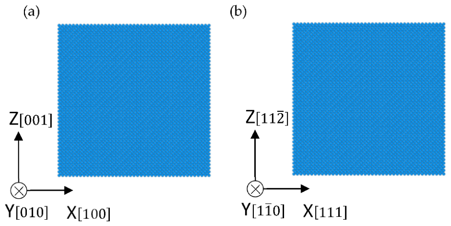
Figure 2.
Stress–strain curves of silicon crystals under tensile and compressive deformation: (a) tension; (b) compression.
Figure 2.
Stress–strain curves of silicon crystals under tensile and compressive deformation: (a) tension; (b) compression.
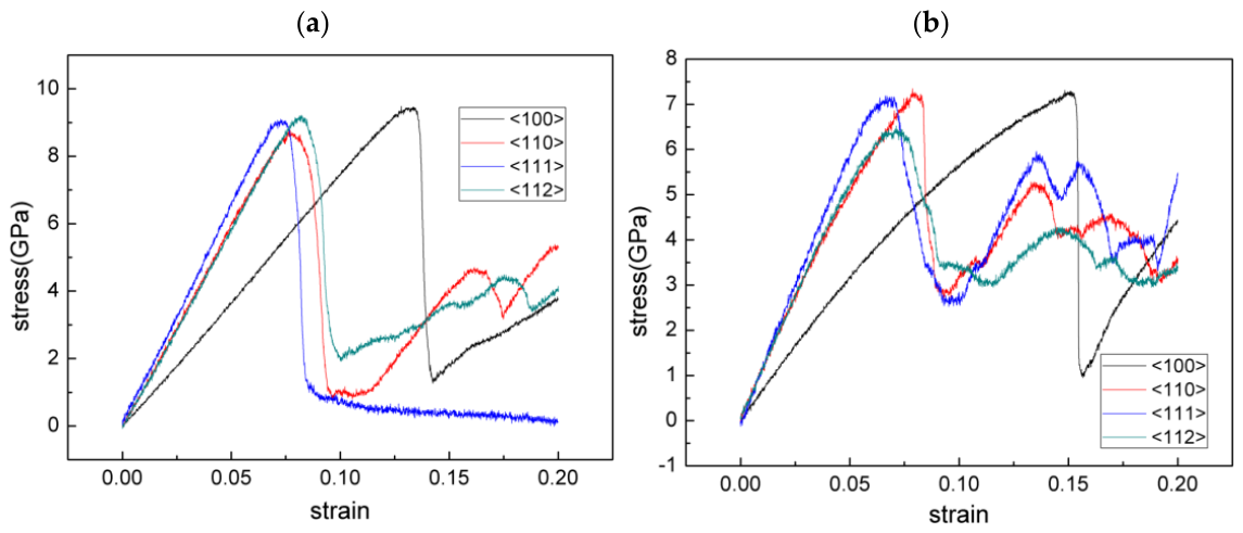
Figure 3.
Linear fits to the elastic portions of the stress–strain curves: (a) tension; (b) compression.
Figure 3.
Linear fits to the elastic portions of the stress–strain curves: (a) tension; (b) compression.
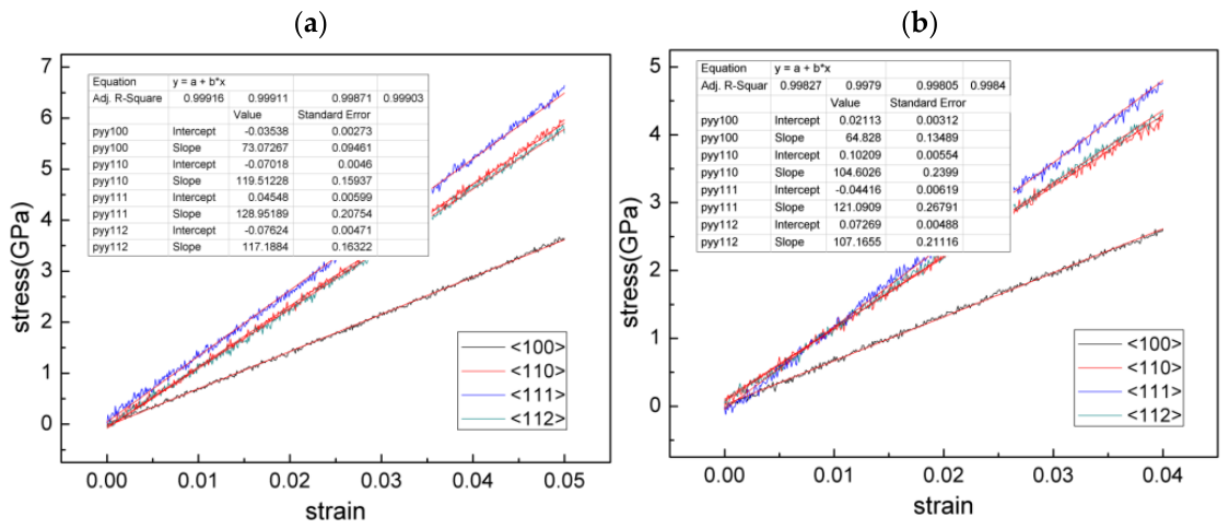
Figure 4.
Snapshot of brittle fracture along the (111) plane of a silicon crystal during tensile deformation along the [111] direction at high temperature (blue spheres denote diamond cubic atoms; gray spheres denote defect or amorphous atoms).
Figure 4.
Snapshot of brittle fracture along the (111) plane of a silicon crystal during tensile deformation along the [111] direction at high temperature (blue spheres denote diamond cubic atoms; gray spheres denote defect or amorphous atoms).
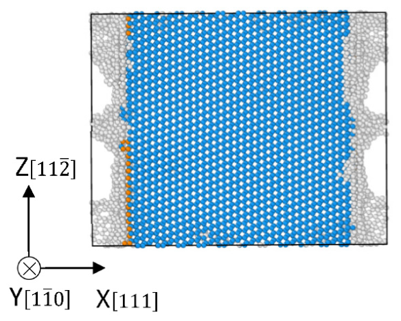
Figure 5.
(a) Fraction of atoms retaining the diamond cubic lattice as a function of strain during deformation along the direction of the Si crystal; (b) evolution of the amorphous fraction and the stress during compression along the direction.
Figure 5.
(a) Fraction of atoms retaining the diamond cubic lattice as a function of strain during deformation along the direction of the Si crystal; (b) evolution of the amorphous fraction and the stress during compression along the direction.
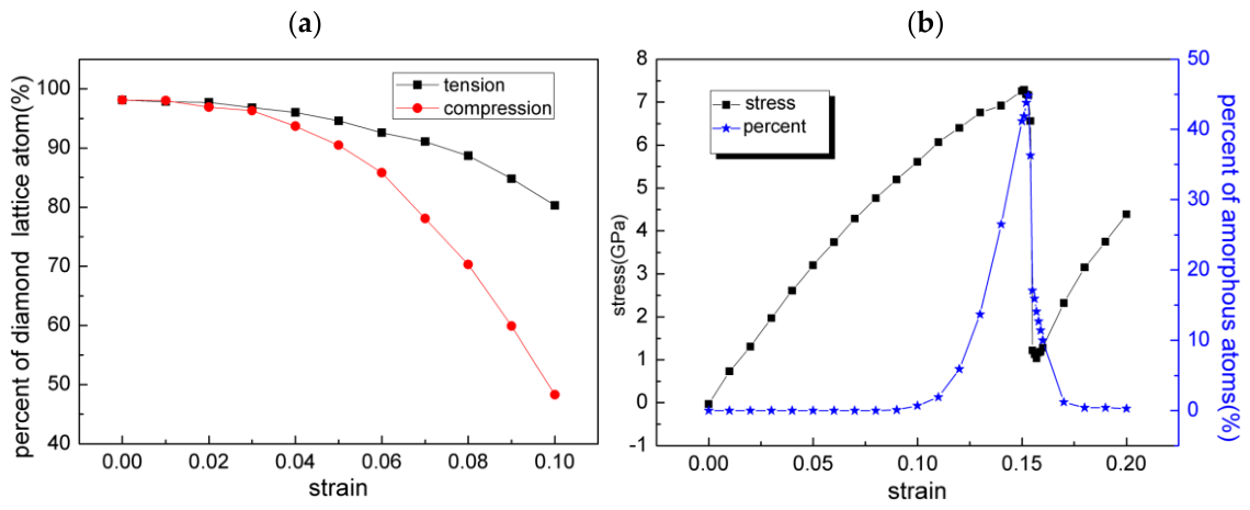
Figure 6.
(a) Spatial distribution of the amorphous atoms in the system (gray spheres denote defect or amorphous atoms; crystalline atoms are omitted for clarity); (b) radial distribution function of the amorphous silicon.
Figure 6.
(a) Spatial distribution of the amorphous atoms in the system (gray spheres denote defect or amorphous atoms; crystalline atoms are omitted for clarity); (b) radial distribution function of the amorphous silicon.
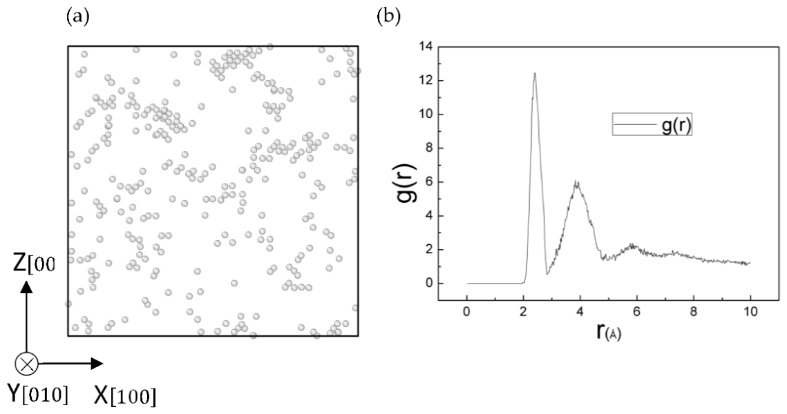
Figure 7.
(a) Dislocations in the silicon crystal at the onset of plasticity; (b) dislocation network formed at larger strains (crystalline atoms are omitted for clarity; the green lines denote Shockley partial dislocations, the red lines full dislocations, and the magenta lines Lomer–Cottrell dislocations; the arrows indicate neither the magnitude nor the direction of the Burgers vector).
Figure 7.
(a) Dislocations in the silicon crystal at the onset of plasticity; (b) dislocation network formed at larger strains (crystalline atoms are omitted for clarity; the green lines denote Shockley partial dislocations, the red lines full dislocations, and the magenta lines Lomer–Cottrell dislocations; the arrows indicate neither the magnitude nor the direction of the Burgers vector).
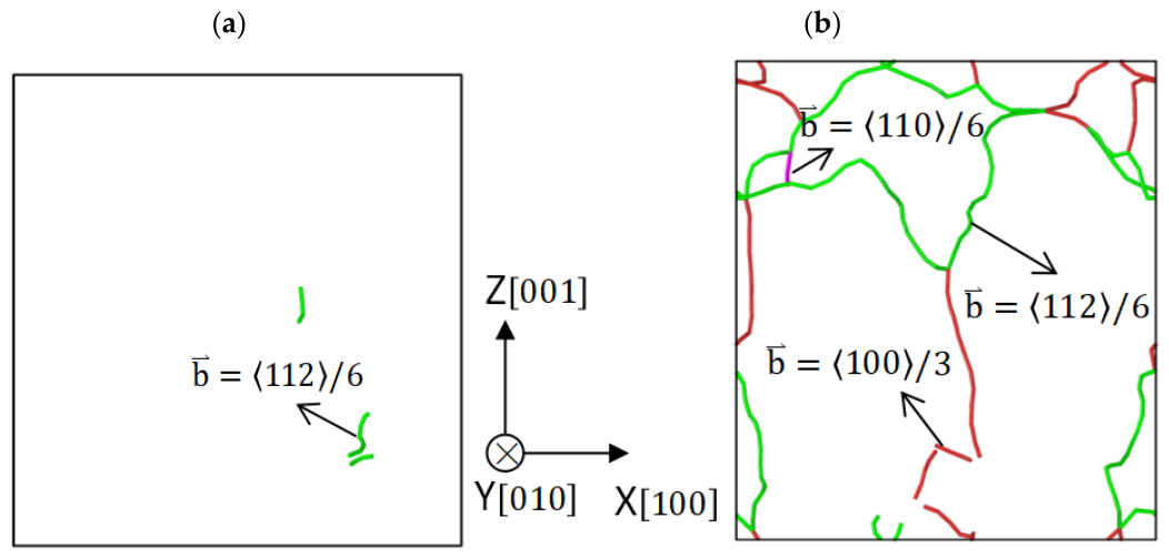
Figure 8.
Projected local structure around the stacking fault and the Shockley partial dislocation during the strain-hardening stage: (a) (111) plane; (b) (110) plane (blue spheres denote diamond cubic atoms, orange spheres HCP-coordinated atoms, gray spheres defect or amorphous atoms, and green lines Shockley partial dislocations).
Figure 8.
Projected local structure around the stacking fault and the Shockley partial dislocation during the strain-hardening stage: (a) (111) plane; (b) (110) plane (blue spheres denote diamond cubic atoms, orange spheres HCP-coordinated atoms, gray spheres defect or amorphous atoms, and green lines Shockley partial dislocations).
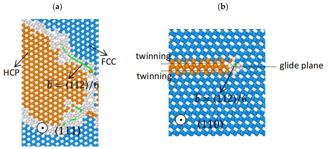

Table 1.
Young's modulus and upper yield strength under tensile and compressive deformation at high temperature.
Table 1.
Young's modulus and upper yield strength under tensile and compressive deformation at high temperature.
| Direction | Tension | Compression | ||
| Young's modulus (GPa) |
Yield strength (GPa) |
Young's modulus (GPa) |
Yield strength (GPa) |
|
| 73.07 | 9.36 | 64.82 | 7.23 | |
| 119.51 | 8.59 | 104.6 | 7.31 | |
| 128.95 | N/A | 121.09 | 7.18 | |
| 117.19 | 9.14 | 107.17 | 6.52 | |
Disclaimer/Publisher’s Note: The statements, opinions and data contained in all publications are solely those of the individual author(s) and contributor(s) and not of MDPI and/or the editor(s). MDPI and/or the editor(s) disclaim responsibility for any injury to people or property resulting from any ideas, methods, instructions or products referred to in the content. |
© 2026 by the authors. Licensee MDPI, Basel, Switzerland. This article is an open access article distributed under the terms and conditions of the Creative Commons Attribution (CC BY) license (http://creativecommons.org/licenses/by/4.0/).
Copyright: This open access article is published under a Creative Commons CC BY 4.0 license, which permit the free download, distribution, and reuse, provided that the author and preprint are cited in any reuse.