

Submitted:
20 August 2026
Posted:
24 August 2026
You are already at the latest version
Abstract
For six decades Moore's Law has guided the semiconductor industry, but dimensional scaling is now meeting hard physical and economic limits. Here we argue that the post-Moore era needs a figure of merit anchored to physical invariants rather than to calendar time. We introduce the spatiotemporal efficiency \(\Lambda = N f /(P V)\), combining transistor count \(N\), clock frequency \(f\), power \(P\) and heat-dissipating volume \(V\). Once the total switching power is accounted for, both \(N\) and \(f\) cancel and \(\Lambda\) reduces to the device energy efficiency divided by volume. Because the thermal resistance of a three-dimensional stack grows linearly with height, \(\Lambda\) falls as \(1/V\)—a relation we call the Volume-Inverse Law. Bounded by Planck's constant and the Landauer limit, it recasts the central competition of the post-Moore era as computation per unit volume, and predicts a finite optimal stacking height and a decisive shift toward energy-efficient, architecture-led design.
Keywords:
post-Moore era
; spatiotemporal efficiency
; Volume-Inverse Law
; Landauer limit
; dimensional scaling
Introduction
In 1965, Gordon Moore observed that the number of transistors on an integrated circuit roughly doubled every 18 to 24 months [10]. Though never a physical law, this empirical projection became the “first principle” of the global semiconductor industry for over half a century—serving both as a technological roadmap and an economic promise: performance increases while costs decrease.
However, this trajectory is approaching its end. As processes enter the 2-nanometer era, dimensional scaling approaches fundamental atomic limits [11]. When transistor gate widths shrink to the scale of a dozen silicon atoms, quantum tunneling causes electrons to leak uncontrollably, severely degrading energy efficiency. Concurrently, economic costs have skyrocketed: an advanced 3nm fabrication facility now requires over $20 billion in investment [1]. NVIDIA CEO Jensen Huang declared in 2022 that “Moore’s Law is dead.” Scholars predict the effective end of Moore’s Law will occur within the 2025–2030 timeframe [1].
The question is no longer whether Moore’s Law will end, but what physical invariant will guide the industry thereafter. This paper seeks to answer that question by proposing a framework that can guide the industry much like Moore’s Law did, but within the constraints of the 3D era.
The Fundamental Dilemma of Moore’s Law: The Absence of an Invariant
To understand the necessity of a new paradigm, we must first dissect the structural weakness of Moore’s Law.
Moore’s Law is, at its core, an empirical fit—it describes what happened, not why it happened. Like Kepler’s laws describing planetary orbits without explaining their mechanical roots, Moore’s Law charts exponential growth in transistor density over time but anchors itself to no physical invariant. Its independent variable is time; its dependent variable is transistor density. Engineers race against the calendar to meet the “18-month doubling” target, yet cannot answer the fundamental question: When time is no longer a uniform variable, does this law still hold?
The arrival of physical limits shatters the assumption of uniform time. As transistor dimensions approach atomic scales, further spatial compression (minimizing ) causes momentum uncertainty to surge, leading to uncontrolled energy dissipation (heating). Conversely, further temporal compression (minimizing ) results in energy fluctuations that cause leakage and crosstalk. Beneath these phenomena lies a deeper physical constraint—the Heisenberg Uncertainty Principle:
This implies that space and time cannot be compressed independently and infinitely. Moore’s Law focuses solely on the single dimension of “spatial scaling.” When spatial compression approaches its limit, a roadmap based purely on “doubling transistor count” inevitably fails.
A Practitioner’s Perspective: The Historical Pattern of Overcoming Roadblocks
The claim that Moore’s Law is ending must be weighed against a sobering historical fact: it has been declared dead many times before, and each time engineering ingenuity revived it. One of us (E.X.W.) spent two decades in CMOS process and device development at Intel and witnessed this pattern firsthand.
The engine beneath Moore’s Law was never transistor count alone but Dennard scaling [9]—the transistor scaling law under which shrinking the feature size while proportionally reducing the supply voltage yielded, at roughly constant power density, simultaneous gains in switching speed and integration density. Through the single-core era, each new process node delivered higher clock frequencies almost for free.
That free lunch ended abruptly at the thermal wall. By the Pentium 4 generation, voltage scaling had effectively stalled while clock frequency continued to climb, so the power density of a physically small die grew faster than any air-cooled package could remove the heat. Frequency saturated near 4 GHz and the single-core roadmap collapsed. The industry’s answer was not to defeat the wall but to route around it: abandoning the pursuit of ever-higher single-thread frequency in favor of multicore parallelism. Moore’s Law—as a statement about transistors per chip—continued.
A second roadblock appeared inside the transistor itself. As the SiO2 gate dielectric thinned to only a few atomic layers, direct quantum-mechanical tunneling of electrons through the gate became a first-order contributor to power consumption, injecting a leakage current that no circuit technique could suppress. The solution came from materials science: replacing SiO2 with a hafnium-based high-k dielectric (introduced at Intel’s 45 nm high-k/metal-gate node in 2007), which restored the required gate capacitance with a physically thicker barrier and cut gate-tunneling leakage by orders of magnitude. Once again, Moore’s Law continued.
The lesson from the trenches is consistent: whenever a specific technical obstacle threatened the roadmap, engineers found a solution and scaling resumed. This history is precisely why proclamations of Moore’s Law’s death are, rightly, met with skepticism. Yet the same history sharpens the central question of this paper. Every one of those victories was won against an engineering constraint—a constraint with headroom, susceptible to a cleverer material, architecture, or process. The thermal wall was relaxed by parallelism; gate leakage was relaxed by a new dielectric. What we confront now is categorically different: limits set not by the current state of engineering but by physical invariants—Planck’s constant h and Boltzmann’s constant . No material lowers h, and no architecture repeals the Landauer bound. The remainder of this paper argues that the post-Moore roadmap must therefore be anchored not to yet another clever fix, but to these immovable constants.
Existing Alternatives and Their Limitations
From Planar to Volumetric: 3D Stacking and Chiplet
The most intuitive extension is moving from two-dimensional planar chips to three-dimensional space. 3D IC technology vertically stacks multiple compute and memory dies, constructing a “skyscraper” of silicon. Industry reports indicate that 3D integration can achieve substantial increases in transistor density while maintaining energy efficiency advantages [5]. Vertical integration dramatically shortens data paths, alleviating the “memory wall” bottleneck.
Chiplet technology decomposes large monolithic dies into smaller chiplets that are heterogeneously integrated, achieving system-level performance breakthroughs. The common characteristic of these approaches is: abandoning extreme scaling of a single die in favor of system-level performance enhancement through three-dimensional spatial expansion.
However, 3D stacking is not a panacea. Vertical stacking leads to a multiplicative increase in power density, making heat dissipation a new bottleneck. It changes the mode of performance improvement—from “compressing area” to “expanding volume”—but still fails to answer the question: Where is the limit?
From Space to Time: Huawei’s Tau () Scaling Law
In May 2026, Huawei formally proposed the Tau () Scaling Law at the IEEE International Symposium on Circuits and Systems (ISCAS) [2]. This marks a significant introduction of an industry-level evolutionary principle in the global semiconductor arena.
The core of the Tau Scaling Law is the replacement of “geometric scaling” with “temporal scaling”. is the time constant in circuit theory (), determining response speed, signal delay, and power consumption. The law targets system-level reduction of across devices, circuits, chips, and systems. Its key technique, “logic folding,” folds planar circuits into three dimensions, shortening interconnect lengths by 50%–80%, improving transistor density by 2–5×, boosting performance by 30%–100%, and reducing power consumption by over 40% [2]. Over the past six years, Huawei has designed and mass-produced 381 chips based on the Tau Scaling Law, with projections to achieve transistor density equivalent to a 1.4nm process by 2031 [2].
The Tau Scaling Law’s breakthrough lies in shifting the optimization target from “spatial dimensions” to “signal time.” Nevertheless, it remains an empirical law centered on a single variable (). It answers what to optimize, but not where the limit lies. It lacks an invariant—a quantity that remains conserved across scaling and process evolution-to anchor the boundary of development.
The Spatiotemporal Law: Reconstructing the Evaluation Framework with Invariants
Physical Invariants: Planck’s Constant h and Boltzmann’s Constant
We posit that the ultimate constraints on semiconductor development arise from two fundamental physical constants: Planck’s constant h (and its reduced form ℏ) and Boltzmann’s constant .
The Heisenberg Uncertainty Principle originates from h—the quantum of action, the source of all quantum uncertainty. Every effective logic operation requires a minimum energy related to the switching time : . The history of semiconductor development is, in essence, the continuous optimization of the allocation between space (V) and time (t) under this invariant h.
Concurrently, Landauer’s principle imposes another constraint: erasing one bit of information dissipates at least of heat [3]. This implies computation is bounded not only by quantum limits but also by thermodynamic limits—an insurmountable boundary between power dissipation, temperature, and information processing rate.
Definition and Derivation of the Spatiotemporal Efficiency
Based on the above analysis, we propose a system-level evaluation metric—Spatiotemporal Efficiency :
where:
- N: effective total number of transistors in the chip or system;
- V: effective heat-dissipating volume (cm3), defined as the physical volume of the chip stack that contributes to heat removal through the primary cooling surfaces. For a stack of n dies each of thickness and lateral area A, to first order, though effective volume may be modified by thermal spreading resistance;
- P: steady-state power dissipation of the chip (W);
- f: operating clock frequency (Hz).
To make this metric physically predictive, we express P in terms of fundamental device parameters. In the dynamic-power-dominant regime, the total switching power of a chip containing N transistors is
where is the switching activity factor, is the average switched capacitance per transistor, and is the supply voltage. It is essential that the transistor count N appear explicitly: the power a package must remove scales with the number of switching devices, not with a single transistor.
This is already a striking result. The metric can be rewritten as
where is the computational energy efficiency (useful operations per joule), which for a fixed device technology and supply voltage is a constant set by , the energy dissipated per switching event. Neither raw transistor count nor clock frequency enters on its own; only their ratio to power—the energy efficiency—does, and volume therefore emerges as the governing variable. Frequency has not become irrelevant: as the thermal analysis below shows, it is a dependent quantity fixed by the available thermal budget rather than a free lever for improving .
Voltage-Frequency Coupling and Thermal Constraints
The maximum operating frequency of a CMOS circuit is constrained by the RC delay, which can be modeled as a function of supply voltage [6]:
where is the threshold voltage, is the velocity saturation index ( for modern devices), and K is a process-dependent constant.
Conversely, the thermal constraint imposes a maximum allowable power density determined by the package’s thermal resistance :
where is the maximum junction temperature and is the ambient temperature.
For a 3D stack with n layers, the thermal resistance scales significantly with volume. Assuming a stack where each layer has thickness and lateral area A, the total thermal resistance can be approximated as:
where is the effective thermal conductivity and are thermal interface resistances. For large n, the interface terms become significant, and the dominant contribution scales linearly with the number of layers: .
Derivation of the Volume-Inverse Law
We now derive the scaling of with V under the thermal constraint.
Key assumptions for the derivation: (i) The chip operates in the super-threshold regime (), where is constrained by noise margins and process requirements rather than being a free scaling parameter; (ii) The thermal resistance scales linearly with volume, ; (iii) Dynamic power dominates, so the total switching power is ; (iv) Transistor count scales linearly with the number of stacking layers, .
First, consider operation at the thermal limit. The maximum power P is fixed by the thermal budget and scales inversely with volume due to the linear increase in :
Second, the achievable clock frequency f at this thermal limit follows from equating the total switching power, Eq. (3), to the thermal budget, Eq. (7). Solving for f and using together with :
A critical insight arises here: in the super-threshold regime relevant to high-performance computing, the supply voltage is not a free scaling parameter. It is pinned near-constant by noise margins, process variations, and reliability requirements (), and cannot be reduced arbitrarily without incurring exponential frequency penalties as the circuit enters the sub-threshold regime. With fixed, the thermal-limited frequency therefore falls quadratically with volume,
because a taller stack must both remove less heat (larger ) and share that shrinking budget among more transistors.
Third, the transistor count N scales linearly with the number of layers:
The corresponding useful throughput is : stacking more layers actually lowers the total operations per second delivered at the thermal limit, because the quadratic frequency penalty outruns the linear gain in device count. Finally, substituting Eqs. (9), (11), and (12) into the definition of reproduces Eq. (4):
This confirms the Volume-Inverse Law:
This result is striking: although the raw transistor count N grows linearly with volume, the efficiency —useful throughput per watt per unit volume—degrades as . The thermal bottleneck forces the power budget to fall as and the clock frequency as , so even the useful throughput declines as . Adding silicon by stacking buys transistors that cannot all be clocked.
Summary of the Volume-Inverse Law
The derivation above shows that the Volume-Inverse Law is the joint consequence of the scaling relations collected in Table 1 and illustrated in Figure 1(a). Two independent routes lead to it: directly, because with a constant energy efficiency (Eq. 5); and, at the thermal limit, because the falling throughput () and the falling power budget () combine as .
The physical implications can be summarized in three layers:
First, time is the manifestation, volume is the foundation. The nominal GHz value of a chip is essentially just the maximum operable frequency under given packaging heat-dissipation capacity and supply voltage. Frequency is a dependent variable; three-dimensional heat-dissipating volume is the independent constraint.
Second, voltage is the sole engineering lever. is strongly dependent on the square of the supply voltage . The only evolutionary direction for future chips is to approach the sub-threshold voltage regime (V), using the quadratic reduction in voltage to offset the energy efficiency degradation imposed by volume expansion, despite the accompanying frequency penalty.
Third, the curse of linear diminishing returns in 3D stacking. Even if chips are stacked into a “skyscraper,” the energy efficiency return per unit volume decreases linearly with stacking layers—the higher the stack, the smaller the marginal gain. Planck’s constant draws the absolute ceiling; humanity can never surpass this boundary, only seek the most elegant “spatiotemporal trade-off” at its edge.
Time Evolution and the Crossover from Moore’s Law
The Volume-Inverse Law is not a statement about transistor count over time, but about efficiency at a given volume. To relate it to Moore’s Law, we can estimate the crossover point: as long as the dominant scaling mechanism is area reduction (i.e., shrinking V per transistor), the traditional Moore scaling holds. Once 3D stacking becomes necessary to continue increasing N, the efficiency begins to degrade.
Let be the technology node feature size; then planar transistor density , and chip volume scales with times the die area. Historically, Moore’s Law gave . The Volume-Inverse Law suggests that when N is increased by stacking, the efficiency drops. The transition occurs when the gain from stacking is offset by the voltage reduction required. Based on current trends, this crossover is expected around the 3nm–2nm node, consistent with industry projections [1].
Distinguishing Quantum and Classical Regimes
The two invariants h and dominate in different regimes. For large feature sizes (nm), thermal noise and Landauer’s limit are the primary constraints; quantum tunneling is negligible. As dimensions shrink below 10nm, quantum effects (tunneling, uncertainty) become increasingly important. In the deep sub-threshold region, both effects coexist.
A useful phase diagram places the operating region of typical chips on a plane of transistor density vs. power density; the Volume-Inverse Law applies across the entire region, but the specific scaling exponents may vary. In the classical regime, ; in the quantum-limited regime, is further bounded by , making the inverse-volume dependence even more stringent.
Discussion: Implications and Predictions
Optimal 3D Stacking Height
Written in terms of the discrete layer count (with denoting thermal, not electrical, resistance), the efficiency inherits the same inverse law,
so decreases monotonically with height: the minimal model contains no interior maximum, and on efficiency grounds alone a single layer is optimal. A finite optimum emerges once the benefits of stacking that this minimal model omits are restored—chiefly the shortening of global interconnects. Partitioning a planar design across n tiers reduces the average wire length as [7,8], which raises the interconnect-limited clock frequency; the system throughput therefore rises while wiring is the binding constraint, and only begins to fall once the thermal-limited frequency of Eq. (11) () takes over. The achievable throughput is the lower envelope of these two regimes and peaks at their crossover (Figure 1(b)). The location of that peak is set by where thermal resistance turns super-linear (interface layers begin to dominate) or where frequency degradation becomes exponential (the sub-threshold onset). Using thermal-interface-resistance data [5], this sweet spot falls between roughly 4 and 8 layers for current cooling technologies, beyond which efficiency drops sharply.
Economic Consequences
The diminishing returns of 3D stacking imply that the semiconductor industry will face a rising cost per unit performance gain. The Volume-Inverse Law provides a physical basis for the economic slowdown: further investment in fabrication facilities may yield only marginal improvements. This suggests a shift from “more transistors” to “more efficient use of transistors” through advanced architectures (e.g., in-memory computing, analog computing, and specialized accelerators) [4].
Connection to Information Density
Writing in terms of information density and energy density shows that, as volume grows, the attainable information density at fixed energy density falls—consistent with Landauer’s principle that more volume implies more entropy generation per bit.
Nonlinear Effects in Real Stacks
Our analysis assumed linear thermal resistance scaling. In practice, thermal interface resistance, hot spots, and coefficient of thermal expansion mismatches introduce additional non-linearities that may make the inverse-volume law even more pessimistic. For example, interlayer thermal resistance can be a significant fraction of total , and its dependence on pressure and surface roughness can cause super-linear growth with n [5]. This reinforces the conclusion that volume expansion is not a free lunch.
A New Coordinate System for the Post-Moore Era
Where Moore’s Law offered a single “North Star”—transistor density on a plane— offers a successor figure of merit that folds throughput, power and volume into one number and applies uniformly across planar chips, 3D stacks, chiplets and domain-specific accelerators. It shifts the question from “how many transistors” to “how efficiently is each unit of volume used.” The resulting roadmap has three stages: near-term volumetric integration, choosing a stacking height near –8; mid-term voltage-limited scaling, pushing toward the sub-threshold regime to exploit the dependence of ; and long-term architectural specialization, where in-memory and analog accelerators raise the efficiency coefficient once and V are exhausted.
This reframing carries an industrial corollary. Value migrates from lithographic shrinking to system-level integration—advanced packaging, thermal-interface materials and heterogeneous integration—and rewards collaboration across physics, materials science and architecture to push toward the Landauer limit. Moore’s Law promised “faster and cheaper”; the Volume-Inverse Law promises “efficient and sustainable.”
Limitations and Scope
Before concluding, it is important to state the scope and limitations of the proposed framework. The Volume-Inverse Law is derived under the following assumptions:
- 1.
- Super-threshold operation: The analysis assumes , where the supply voltage is constrained by noise margins and reliability rather than being a free scaling parameter. In the sub-threshold regime, the voltage-frequency relationship becomes exponential, and the scaling exponent of with respect to V may differ.
- 2.
- Linear thermal resistance scaling: The model assumes for the dominant contribution. Advanced cooling technologies (e.g., microfluidic cooling, interlayer thermal vias) or monolithic 3D integration with ultra-low interface resistance could alter this scaling.
- 3.
- Dynamic-power dominance: Leakage power is neglected. At very low voltages (deep sub-threshold) or high temperatures, leakage contributions may become significant and modify the scaling behavior.
- 4.
- Constant transistor density per layer: The law assumes each stacking layer has the same transistor density. Heterogeneous integration with varying densities across layers would require a more nuanced model.
- 5.
- Conventional CMOS technology: The framework is developed for conventional CMOS-based digital logic. Emerging technologies (e.g., superconducting logic, optical computing, quantum computing) operate under fundamentally different physical constraints.
Within these bounds, the Volume-Inverse Law provides a robust physical limit for conventional 3D-stacked CMOS systems. The law should be viewed as a guiding physical bound rather than a universal empirical curve applicable to all computing paradigms. It identifies the fundamental trade-off space, allowing engineers to optimize within the constraints.
Conclusion: From Empirical Table to Fundamental Logic
Moore’s Law cannot simply be “replaced.” It is the semiconductor industry’s empirical table—a precise description of transistor growth that, like Kepler’s laws before Newton, lacks the physical invariants needed to explain why. When physical limits break the assumption of uniform time, that table loses its predictive power.
Spatiotemporal efficiency , and the Volume-Inverse Law derived from it, constitute the semiconductor industry’s “fundamental logic.” Anchored by Planck’s constant h and Boltzmann’s constant as invariants, it unifies all optimization directions—dimensional scaling, temporal compression, three-dimensional stacking, architectural innovation—within a single evaluation framework. It offers not an “18-month doubling” calendar promise, but a physical upper bound on “how much computation can be extracted per unit volume at the quantum-thermodynamic boundary.”
In the future, the industry will continue to speak of “equivalent nanometers,” just as astronomers still speak of “planetary orbits.” But the underlying coordinate system that determines the industry’s direction will shift from a “dimensional race” to a “volumetric efficiency race.” Moore’s Law defined the semiconductor industry’s adolescence—the era of competing over who grows faster; the Volume-Inverse Law will define its maturity—the era of competing over who lives most gracefully before the eternal physical invariants.
Predictions for the Industry
Based on our framework, we offer four concrete predictions:
- 1.
- The optimal number of stacked layers in commercial 3D ICs will converge to 4–8, with further stacking showing negligible performance-per-watt improvement relative to the increased cost.
- 2.
- Supply voltages will continue to decrease toward 0.2–0.3V, but performance gains (frequency scaling) will be modest as frequency scales inversely with thermal resistance.
- 3.
- Architectural innovations (e.g., near-memory computing, analog processing, in-memory computing) will become more important than pure transistor scaling for continued efficiency improvements.
- 4.
- The semiconductor value chain will pivot towards advanced packaging and thermal management, reflecting the shift from planar to volumetric constraints. Investment in packaging R&D will eventually exceed investment in front-end lithography.
Data Availability Statement
No datasets were generated or analysed for this Perspective; all quantitative relations are derived analytically in the main text.
Conflicts of Interest
The authors declare no competing interests.
References
- Zhang, R.; Liu, M.; Zhu, N. H.; Tang, H.; Liu, K. A new path and novel technology for integration beyond the Moore era—review of the 393rd ’Shuangqing Forum’. Sci. Sin. Informationis 2025, vol. 55(no. 6), 1350–1371. [Google Scholar] [CrossRef]
- He, T. A Time Scaling Theory for Multi-Layer Electronic Systems 202605. ChinaXiv. 00224v1 May 2026. Available online: https://chinaxiv.org/abs/202605.00224.
- Landauer, R. Irreversibility and Heat Generation in the Computing Process. IBM J. Res. Dev. 1961, vol. 5(no. 3), 183–191. [Google Scholar] [CrossRef]
- Davies, M.; Sankaralingam, K. Defying Moore: Envisioning the Economics of a Semiconductor Revolution through 12nm Specialization. Commun. ACM 2025, vol. 68(no. 7), 108–119. [Google Scholar] [CrossRef]
- Rahman, A.; Reif, R. Thermal Analysis of Three-Dimensional (3-D) Integrated Circuits (ICs). In Proceedings of the IEEE International Interconnect Technology Conference (IITC), Burlingame, CA, USA, June 2001; pp. 157–159. [Google Scholar]
- Chandrakasan, A.; Brodersen, R. Low-Power Digital CMOS Design; Kluwer Academic Publishers, 1995. [Google Scholar]
- Rahman, A.; Reif, R. System-Level Performance Evaluation of Three-Dimensional Integrated Circuits. IEEE Trans. Very Large Scale Integr. (VLSI) Systems 2000, vol. 8(no. 6), 671–678. [Google Scholar] [CrossRef]
- Banerjee, K.; Souri, S. J.; Kapur, P.; Saraswat, K. C. 3-D ICs: A Novel Chip Design for Improving Deep-Submicrometer Interconnect Performance and Systems-on-Chip Integration. Proc. IEEE 2001, vol. 89(no. 5), 602–633. [Google Scholar] [CrossRef]
- Dennard, R. H.; Gaensslen, F. H.; Yu, H.-N.; Rideout, V. L.; Bassous, E.; LeBlanc, A. R. Design of Ion-Implanted MOSFET’s with Very Small Physical Dimensions. IEEE J. Solid-State Circuits 1974, vol. 9(no. 5), 256–268. [Google Scholar] [CrossRef]
- Moore, G. E. Cramming more components onto integrated circuits. Electronics 1965, vol. 38(no. 8), 114–117. [Google Scholar]
- Keyes, R. W. Physical limits in digital electronics. Proc. IEEE 1975, vol. 63(no. 5), 740–767. [Google Scholar] [CrossRef]
Figure 1.
The Volume-Inverse Law. (a) Log–log scaling of the key quantities with heat-dissipating volume V (equivalently stack height ) at the thermal limit and fixed supply voltage: transistor count , power budget , and clock frequency combine so that the spatiotemporal efficiency (thick curve); the useful throughput shares the slope. (b) Origin of a finite optimal stacking height as the crossover of two competing mechanisms. Stacking shortens global interconnects—the average wire length of a design partitioned across n tiers scales as [7,8]—which raises the interconnect-limited throughput (rising branch); meanwhile the thermal-limited throughput falls as (Eq. 11). The achievable throughput is the lower envelope of the two and peaks at their crossover, within the shaded –8 band.
Figure 1.
The Volume-Inverse Law. (a) Log–log scaling of the key quantities with heat-dissipating volume V (equivalently stack height ) at the thermal limit and fixed supply voltage: transistor count , power budget , and clock frequency combine so that the spatiotemporal efficiency (thick curve); the useful throughput shares the slope. (b) Origin of a finite optimal stacking height as the crossover of two competing mechanisms. Stacking shortens global interconnects—the average wire length of a design partitioned across n tiers scales as [7,8]—which raises the interconnect-limited throughput (rising branch); meanwhile the thermal-limited throughput falls as (Eq. 11). The achievable throughput is the lower envelope of the two and peaks at their crossover, within the shaded –8 band.
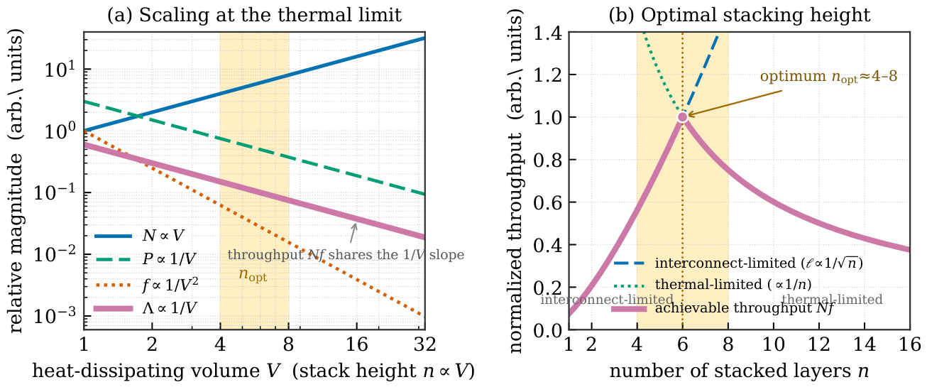

Table 1.
Scaling of the key quantities with heat-dissipating volume V (equivalently, with stack height ) at the thermal limit, for fixed supply voltage .
Table 1.
Scaling of the key quantities with heat-dissipating volume V (equivalently, with stack height ) at the thermal limit, for fixed supply voltage .
| Quantity | Scaling | Origin |
|---|---|---|
| Transistor count N | one device layer per unit height | |
| Thermal resistance | series conduction through the stack | |
| Power budget P | ||
| Clock frequency f | fixed budget shared among N devices | |
| Throughput | linear gain vs. quadratic penalty | |
| Efficiency |
Disclaimer/Publisher’s Note: The statements, opinions and data contained in all publications are solely those of the individual author(s) and contributor(s) and not of MDPI and/or the editor(s). MDPI and/or the editor(s) disclaim responsibility for any injury to people or property resulting from any ideas, methods, instructions or products referred to in the content. |
© 2026 by the authors. Licensee MDPI, Basel, Switzerland. This article is an open access article distributed under the terms and conditions of the Creative Commons Attribution (CC BY) license (http://creativecommons.org/licenses/by/4.0/).
Copyright: This open access article is published under a Creative Commons CC BY 4.0 license, which permit the free download, distribution, and reuse, provided that the author and preprint are cited in any reuse.