
Submitted:
19 August 2026
Posted:
20 August 2026
You are already at the latest version
Abstract
To meet the fast-response and wide load-current requirements of X-ray detector readout chips, a Low-Dropout regulator (LDO) based on an improved Level-Shifted Flipped Voltage Follower (LS FVF) is proposed in a 130-nm CMOS. A fast Flipped Voltage Follower (FVF)-based feedback loop is introduced to improve transient response, while a level shifter is introduced to relax the dc operating-point coupling between the pass-transistor gate and the control transistor drain at light loads. To further enhance response speed, dynamic current-source biasing, which senses output-voltage variations through capacitive coupling, is proposed, and it is capable of adaptively increasing the LS FVF driving capability during large load transients. A positive-feedback auxiliary circuit is proposed to further accelerate the charging and discharging of the pass-transistor gate. To maintain stability over the 0–400 mA load range, dynamic pole-zero compensation is combined with Miller compensation to track load-dependent poles and preserve sufficient phase margin across operating conditions. Post-layout simulations with a 200 pF load capacitor and a 0–400 mA load-current step show, an overshoot of 100.4 mV and an undershoot of 50.5 mV, with recovery times of 0.2 μs and 0.12 μs, respectively. The proposed LDO achieves a capacitance-normalized transient figure of merit of 0.113 ps, demonstrating a favorable trade-off among performance parameters.
Keywords:
LDO
; FVF
; fast transient response
; dynamic biasing
; pole-zero compensation
1. Introduction
As X-ray imaging systems evolve toward higher frame rates, greater throughput, and higher levels of integration, detector readout ASICs typically integrate large-scale pixel arrays, multichannel analog front ends, analog-to-digital converters, and high-speed digital processing modules [1,2,3,4,5,6]. During data acquisition and readout, the simultaneous activation of numerous digital circuits and rapid switching between operating states can induce large and abrupt variations in the supply load current. The digital power-management circuitry of the ASIC must therefore provide a fast transient response while maintaining stable operation under such conditions. Meanwhile, the readout ASIC also imposes stringent constraints on the area and power consumption of the power-management circuitry. To address these requirements, this work presents an LDO implemented in a 130-nm CMOS process, operating from a 1.5 V input to provide a 1.2 V output with a 200 pF load capacitance. The proposed LDO achieves fast transient response and stable operation over a load-current range of 0–400 mA.
Conventional LDOs typically employ an Error Amplifier (EA) to drive the power transistor and regulate the output voltage through negative feedback, as illustrated in Figure 1. However, in high-load-current applications, the power transistor generally requires a large device size, resulting in substantial gate parasitic capacitance. This parasitic capacitance, together with the relatively high equivalent output resistance of the EA, results in a large gate charging and discharging time constant and consequently limits the load-transient response speed [7,8,9]. Therefore, accelerating the charging and discharging of the gate of the large power transistor and mitigating the transient-response limitation imposed by its parasitic gate capacitance are key challenges in achieving fast transient performance in high-load-current LDOs.
To address the aforementioned challenges, Flipped Voltage Follower (FVF)-based LDOs, as shown in Figure 2, have attracted considerable attention owing to their fast feedback path and low equivalent impedance [10,11,12,13]. In a conventional FVF, M1 directly senses variations in the output voltage, while the current through M2 modulates the current delivered by the pass transistor MP, allowing load disturbances to bypass the slow feedback path associated with the bandwidth-limited conventional EA and thereby improving the transient response. However, conventional FVFs still suffer from two major limitations when operating over a wide load-current range. First, the gate voltage of the pass transistor MP and the drain voltage of the control transistor M1 are coupled; at light loads, must increase to reduce the overdrive voltage of , which may force M1 into the triode region and consequently cause a deviation in the output voltage. Second, the conventional FVF provides only small transient charging and discharging currents to VPG, resulting in a limited slew rate at VPG and consequently constraining the transient response speed.
To address the first issue, the shared node between the two branches can be decoupled [14,15,16,17]. Albezzano et al. [14] introduced a common-gate stage into the fast feedback loop to form a Cascoded FVF, which redistributes the internal node voltages and enables M1 to maintain an appropriate operating condition over a wider load current range. However, the voltage level shift provided by this structure is relatively limited, approximately equal to the overdrive voltage of the common-gate transistor. To further increase the voltage level shift, a source follower can be employed [15] to form a Level-Shifted FVF (LS FVF). Under a small overdrive voltage condition, its DC voltage level shift can be approximately equal to the threshold voltage. Cai et al. [16] further modified the source follower in the LS FVF into a Super Source Follower (SSF), forming an SSF FVF, which achieves the same voltage level shift as the LS FVF while providing a lower output impedance. However, the SSF FVF requires the output pole to be located at a low frequency to ensure stability, which limits the maximum load current and imposes a minimum load capacitance requirement. To further extend the load current range, Zhu et al. [17] combined the Cascoded FVF and SSF FVF to develop a Buffered FVF (BFVF), which provides an enhanced voltage shift. However, this circuit exhibits degraded stability under no-load conditions. Considering that the application requires a wide load current range, including the no-load condition, the Cascode FVF, SSF FVF, and Buffered FVF structures are not adopted in this design. Instead, the LS FVF structure is employed.
To address the second limitation, the transient response can be improved by increasing the charging and discharging speed of the node of the pass-transistor gate [18,19,20]. Lu et al. [18] introduced dynamic biasing into the FVF to rapidly adjust the bias current of the FVF loop in response to load-current variations, thereby improving the transient response. In this scheme, a common-gate MOS transistor converts variations in the output voltage into current variations, which are then mirrored to modulate the FVF bias current, enabling rapid adjustment of the gate voltage of the large pass transistor and alleviating the gate slew-rate limitation inherent in fixed-bias implementations. However, the load-dependent variation of the internal poles in this topology is relatively complex, posing considerable challenges to stability design over a wide load-current range. To further improve the transient response, Boanloo et al. [19] employed a push–pull technique to enhance the gate slew rate of the pass transistor in the FVF. This approach employs cross-coupled common-gate branches to establish two output-voltage feedback paths. The resulting feedback signals control the push–pull stage to provide larger bidirectional charging and discharging currents, thereby mitigating the slew-rate limitation caused by the limited drive current in conventional FVFs. However, this method requires additional gain stages and signal paths, increasing the number of internal dynamic nodes and substantially complicating frequency compensation and stability design across the entire load range. In addition to the above approaches, Pappiah et al. [20] incorporated a Slew-Rate Enhancer (SRE) into an FVF LDO, where capacitive coupling senses variations in the FVF control voltage and dual current mirrors directly charge and discharge the parasitic gate capacitance of the pass transistor, thereby reducing the output-voltage deviation caused by load transients and shortening the recovery time. However, this design was validated over a narrow load-current range of 0–50 mA, and its transient driving capability for a large pass transistor under load currents of several hundred milliamperes has not yet been sufficiently demonstrated. Considering the stringent chip area constraint and the wide load current range of 0–400 mA in this application, the design combinates dynamic biasing, push-pull driving, and capacitive coupling techniques to enhance the transient response speed.
In addition, frequency compensation of the LDO over a wide load-current range represents another major design challenge, which can be addressed using techniques such as pole splitting, and dynamic compensation [21,22,23].
In summary, although numerous improvements to FVF-based LDOs have been proposed to extend the load-current range and enhance the transient response, several limitations remain. To meet the requirements of the digital power supply in X-ray detector readout ASICs for fast transient response and a wide load-current range, this work proposes an LDO based on an improved LS FVF architecture implemented in a 130-nm CMOS process, as shown in Figure 3. In the proposed design, the source follower in the LS FVF relaxes the coupling between the DC operating points and forms a fast local feedback loop, while its low output impedance enhances the capability to drive the gate of the large power PMOS transistor. Capacitive coupling is further employed to sense transient variations in the output voltage and dynamically adjust the LS FVF bias current, thereby providing the fast feedback loop with enhanced drive capability during load transients. Meanwhile, a positive-feedback auxiliary circuit is proposed to accelerate the transient response of the gate voltage of MP. Moreover, to maintain stability over the entire load-current range, a dynamic pole-zero compensation scheme is adopted, in which the compensation network adjusts the pole and zero locations according to the load condition to accommodate variations in the system poles.
The remainder of this paper is organized as follows: Section 2 analyzes and designs the key modules, including the LS FVF fast loop, dynamic biasing circuit, positive feedback auxiliary circuit, and EA. Section 3 establishes a dual-loop small-signal model, analyzes the system poles and zeros as well as the dynamic pole-zero compensation mechanism, and presents the frequency-compensation design of the LDO. Section 4 presents the LDO layout and post-layout simulation results and compares its performance with prior work in terms of DC characteristics, load-transient response, Power-Supply Rejection Ratio (PSRR), and other key metrics. Finally, Section 5 concludes the paper.
2. Proposed LDO Architecture
2.1. LS FVF Fast Loop Analysis and Design
In this application, the current load varies from 0 to 400 mA, resulting in a wide variation in the gate voltage of the power transistor MP. However, the biasing condition of the conventional FVF is difficult to accommodate such a wide gate voltage range, which may drive the control transistor M1 out of the saturation region and degrade the normal operation of the feedback loop. To address this issue, a level shifter consisting of MLS and MLSP is incorporated into the FVF to form an LS FVF, as shown in Figure 4. By decoupling the gate of MP from the drain of M1, the proposed structure alleviates the a forementioned limitation and enables all transistors to maintain appropriate operating conditions over a wide load range. Furthermore, the source-follower-based level shifter introduced in the LS FVF further reduces the equivalent impedance at the gate node VPG of the power transistor, thereby decreasing the charging and discharging time constant associated with the large gate parasitic capacitance and improving the gate speed of MP. A quantitative analysis of the low-output-impedance characteristic of the LS FVF is presented below.
When a test voltage is applied to the gate node of the power transistor , the small-signal voltage response at the internal node after signal amplification through and the common-gate transistor can be expressed as:
Here, denotes the transconductance of the power transistor MP, and represents the equivalent impedance at node VA, which can be approximated as .
Based on Kirchhoff’s current law at the node, the approximate expression for the small-signal output impedance at can be derived as:
Here, denotes the transconductance of the level-shifting transistor Since the transconductance of the power transistor is sufficiently large and satisfies , the above expression can be further simplified for engineering analysis as:
The charging and discharging time constant at node under LS FVF drive is reduced to:
Here, denotes the time constant at in the conventional FVF shown in Figure 2, where the equivalent resistance at this node is approximately . In the proposed design, , resulting in an that is significantly lower than the equivalent resistance at in the conventional FVF, thereby substantially reducing the associated time constant. Therefore, compared with the conventional FVF, the LS FVF further reduces the equivalent impedance at the gate node of the power transistor, shifting the corresponding pole toward higher frequencies and shortening the small-signal settling time. The large-signal slew rate is instead determined by the charging and discharging currents at the node.
2.2. Analysis and Design of the Capacitive-Coupled Dynamic Biasing Circuit (CCDB) and the Positive Feedback Auxiliary (PFA) Circuits
To address the trade-off between low quiescent current and fast transient response caused by the fixed current biasing in the LS FVF circuit, two auxiliary circuits, namely, a Capacitive-Coupled Dynamic Biasing (CCDB) and a Positive Feedback Auxiliary (PFA) circuit, are introduced to dynamically regulate the charging and discharging currents at , thereby accelerating the transient response. When the load current increases abruptly and decreases, the CCDB circuit raises , thereby increasing the current of and further enhancing the discharging current of . As a result, the voltage at rapidly decreases, increasing the current through to compensate for the load variation and maintain a stable . To further accelerate the charging and discharging of the VPG node, a PFA circuit is proposed, which dynamically adjusts the current of the charging current source and introduces an additional discharge branch to adaptively regulate the discharge current at the node.
2.2.1. Capacitive-Coupled Dynamic Biasing Circuit
The CCDB circuit, highlighted in blue in Figure 5, employs capacitive coupling to sense variations in the output voltage and dynamically adjust the current of the current-source transistor . Under steady-state conditions, capacitor behaves as an open circuit at dc. In this condition, – together with resistor establish a stable dc bias, maintaining at the desired level. Consequently, provides only the baseline tail current required for proper operation of the LS FVF. Therefore, under light-load or steady-output conditions, the fast loop does not continuously operate at a high bias current. When the load current increases abruptly, undergoes a rapid undershoot. This voltage variation is coupled through to the gate of . As decreases, the gate voltage of also drops momentarily, enhancing the conduction of the PMOS transistor and thereby rapidly raising . The resulting increase in increases the current through the LS FVF tail transistor , thereby providing the fast loop with enhanced current-driving capability. Unlike a conventional approach that continuously increases the quiescent bias current, the proposed dynamic biasing technique temporarily enhances the transconductance and drives current of the critical branches only during output transients and restores the circuit to its low-power state once the transient subsides. In the design, the CCDB circuit draws a quiescent current of 15 μA under full-load conditions.
To quantitatively assess the transient-response enhancement achieved by the CCDB circuit, comparative simulations were conducted with the CCDB enabled and disabled, while all other conditions, including the pass-transistor dimensions, LS FVF fast loop, and slow main loop, were kept identical. With a 200-pF load capacitance, the load current was stepped between 0 and 400 mA with a 100-ns transition time, and the resulting transient responses are shown in Figure 6.
Without CCDB, the LDO output voltage drops to a minimum of approximately 1.08 V, corresponding to an undershoot of about 117.2 mV; with CCDB enabled, the minimum output voltage increases to approximately 1.15 V and the undershoot is reduced to about 45.6 mV. Meanwhile, a pronounced reverse overshoot occurs after the initial undershoot when CCDB is disabled, whereas this secondary voltage disturbance is significantly suppressed when CCDB is employed. This improvement arises because the output-voltage drop is coupled to the LS FVF tail-current control node through the CCDB, transiently increasing the effective transconductance of the fast loop and enhancing the gate-discharge capability, thereby allowing the power PMOS transistor to increase the output current more rapidly. When the current load transitions from heavy load to light load, the initial overshoot peaks are similar with and without CCDB, indicating that it does not provide a significant improvement for this transition.
2.2.2. Positive Feedback Auxiliary Circuit
The PFA circuit, highlighted in orange in Figure 5, dynamically regulates the charging and discharging currents of the node. Under steady-state conditions, the PFA provides the gate-bias voltage for the current-source transistor of the level shifter. When the load current increases abruptly, the LS FVF pulls downward, increasing and consequently raising , which reduces the charging current supplied by to and thereby accelerates its voltage drop. To further accelerate the voltage drop at this node, a current mirror formed by and provides an additional discharge path for . Therefore, the PFA circuit adaptively regulates the charging and discharging currents of , further improving the response speed of the LS FVF. The PFA circuit draws a quiescent current of approximately 200 μA under full-load conditions.
To further verify the improvement in transient performance provided by the PFA circuit, comparative load-transient simulations were performed with and without the PFA circuit. Under identical simulation conditions, the load current was switched between 0 and 400 mA with a transition time of 100 ns, while the output load capacitance was maintained at 200 pF. As shown in Figure 7, without the PFA circuit, the limited charging and discharging capability of the LS FVF fast loop at the power-transistor gate node results in a relatively large output-voltage deviation during load transients, with a maximum deviation of approximately 68.9 mV. In contrast, with the PFA circuit enabled, the maximum output-voltage deviation is reduced to approximately 45.6 mV, resulting in a significant improvement in transient performance. This improvement is primarily attributed to the PFA circuit dynamically regulating the charging and discharging of the node.
2.3. Analysis and Design of an RFC-Based EA
In the proposed dual-loop LDO architecture, the slow main loop is primarily responsible for high-accuracy DC regulation and steady-state output-voltage control. As the core building block of the slow main loop, the gain and bandwidth of the EA are key factors determining the LDO’s line regulation, load regulation, and low-frequency PSRR. To enhance both gain and bandwidth without increasing the quiescent power consumption, an EA based on the Recycling Folded-Cascode (RFC) topology is adopted in the design.
Although the conventional Folded-Cascode (FC) amplifier provides a wide input common-mode range and high output resistance, its folded branches are primarily used for DC biasing and small-signal current transfer rather than directly contributing to transconductance amplification, resulting in limited transconductance efficiency per unit bias current. The RFC topology reuses the bias-branch currents of the conventional folded-cascode amplifier, allowing currents that would otherwise contribute only marginally to signal amplification to be converted into effective transconductance, thereby improving the transconductance, unity-gain bandwidth, and slew rate at approximately the same power consumption [24,25,26,27]. As illustrated by the RFC block in Figure 8, the input differential pair is proportionally split, and a cross-coupled current-mirror ratio K is employed to constructively combine the small-signal currents in the folded branches with the input-signal current, thereby substantially enhancing the effective transconductance without increasing the tail bias current. The low-frequency voltage gain of the RFC amplifier, , can be expressed as:
and denote the transconductance and small-signal output resistance, respectively, of transistor in Figure 8, while K represents the current-mirror ratio of the RFC cross-coupled current mirror and is set to 3 in the design.
As shown in Figure 9, the simulated RFC EA achieves a DC gain of approximately 70 dB and a unity-gain bandwidth of 50 MHz while drawing only approximately 65 μA. The high DC gain effectively suppresses the impact of supply disturbances and load-current variations on the output voltage, thereby improving both line and load regulation.
3. Loop Stability and Frequency Compensation Design
The complete circuit of the proposed LDO is shown in Figure 10. Due to the presence of two loops and multiple amplification stages, frequency compensation is required to ensure stable operation. In the design, the load current varies from 0 to 400 mA, causing the pole locations associated with the power transistor to shift by several orders of magnitude due to the variations in its transconductance and output resistance , which poses a significant challenge to system stability. In this section, the loop is broken at the output node to establish the small-signal model of the open-loop system, derive its transfer function, and analyze the frequency compensation mechanism, as illustrated in Figure 11.
Neglecting the poles located well beyond the unity-gain bandwidth, four dominant nodes need to be considered: the EA output node , the LS FVF internal node , the power-transistor gate node , and the output node . Therefore, with the PFA circuit retained while temporarily neglecting the frequency-compensation networks formed by and , the uncompensated open-loop gain can be approximated as:
Here, denotes the magnitude of the equivalent DC loop gain., while , , , and represent the four poles considered in the small-signal model, respectively.
The RFC EA output node exhibits a high output resistance , with its equivalent node capacitance denoted as . Therefore, without the dynamic compensation branch, the absolute value of the corresponding pole can be approximately expressed as . In the design, the RFC EA exhibits a high output impedance and relatively large parasitic capacitance, making the dominant pole of the system. The primary objective of the subsequent compensation scheme is not to alter this low-frequency dominant pole, but rather to control the non-dominant poles that follow and mitigate the additional phase shift introduced by these poles.
The second node that requires consideration is , which is located within the fast path of the LS FVF. If and denote the equivalent small-signal resistance and total parasitic capacitance at this node, respectively, the absolute value of the corresponding pole without compensation can be approximated as . Since is located inside the LS FVF fast loop, its pole directly affects the phase shift of the fast path in the medium- and high-frequency regions. When approaches the unity-gain frequency of the loop, the additional phase lag introduced by this pole combines with those from the other two non-dominant poles, becoming one of the major stability limitations in high-bandwidth designs.
The third critical pole is located at the node. To support a maximum load current of 400 mA, the power transistor requires a large device size, resulting in a substantial parasitic gate capacitance at this node. Accordingly, the absolute value of the pole at can be approximated as:
The fourth critical pole is located at the output node . When is much larger than the parasitic capacitance at the output node, the absolute value of the output pole can be approximated as . Here, denotes the small-signal equivalent resistance at the output node, and is the load capacitance. Unlike the poles associated with the three internal nodes, is highly sensitive to the load current. At light loads, the transconductance of the power transistor decreases while the equivalent output resistance increases, causing the output pole to shift toward lower frequencies and potentially approach the internal non-dominant poles, such that multiple poles may simultaneously fall within the unity-gain bandwidth and significantly degrade system stability. Under heavy-load conditions, the output pole shifts toward higher frequencies, while the power-transistor gate node and the internal node in the fast loop become the primary limitations on stability in the medium- and high-frequency regions.
Therefore, the proposed system does not exhibit a fixed arrangement of non-dominant poles over the entire load range. Instead, it behaves as four poles coupled system whose pole locations vary with the load condition. This load-dependent pole migration is also one of the primary reasons why a fixed single-zero compensation scheme is insufficient to ensure stability over the entire load range.
To increase the separation among the four poles, a Miller compensation branch composed of the series-connected and is first introduced between and . Assuming that the equivalent gain from to is , where , the effective capacitance contributed by the Miller capacitor at can be approximated as , shifting the absolute value of the compensated pole at this node to:
Owing to the Miller multiplication of by the forward gain, the pole at is significantly separated from the subsequent high-frequency poles, thereby producing the well-known pole-splitting effect. In the proposed design, this compensation network is not intended to replace the low-frequency dominant pole at . Instead, it establishes a controlled frequency separation within the fast LS FVF path, thereby preventing the phase contributions of , , and from accumulating within the same frequency range around the unity-gain frequency.
Using the compensation capacitor alone introduces a right-half-plane zero through the feedforward current path. Therefore, a series resistor is employed to control the location of this zero and improve system stability. Denoting the equivalent transconductance of the downstream stages from to the output as , the zero location under the conventional first-order Miller compensation approximation can be expressed as:
When , the zero introduced by the feedforward path through the compensation capacitor is pushed to a very high frequency. By further setting , the zero is shifted into the left-half plane, providing positive phase lead in the mid-frequency region. In the design, and are set to 300 Ω and 29 pF, respectively. remains greater than over the entire load range, thereby improving system stability.
For large load-current variations, the fixed compensation network alone is insufficient to ensure system stability over the entire load range. To address this issue, a dynamic pole-zero compensation network composed of and MOS transistor is further introduced at the node. Unlike a fixed resistor, the equivalent resistance of , denoted as , varies with . In the design, is approximately 30 Ω under no-load conditions, and is . The admittance at this node can be expressed as:
Accordingly, the corresponding impedance can be expressed as:
As indicated by (11), the introduction of the network introduces an additional zero located at . Since in the design, the two poles can be approximately expressed as:
and
Therefore, the resulting pole-zero locations approximately satisfy the frequency relationship .
In the low-frequency region, behaves approximately as an open circuit, allowing the RFC to retain a high output impedance and DC gain without significantly affecting the steady-state regulation of the main loop. In the mid-frequency region, the zero provides phase lead to compensate for the phase lag introduced by the poles at , , and the LDO output, while its location adaptively shifts with the output pole. At higher frequencies, shifts dynamically relative to the output pole to maintain system stability. At light loads, the output pole moves toward the origin. Meanwhile, the EA output voltage decreases, increasing and consequently shifting the introduced zero toward the origin, thereby maintaining sufficient phase margin. Therefore, compared with conventional fixed-zero compensation, the proposed network preserves high low-frequency gain while selectively providing phase boost in the mid-frequency region, where the system stability is most critical.
Based on the above analysis, the compensated loop transfer function can be expressed as:
System stability is ensured by three coordinated frequency-compensation mechanisms. First, the low output impedance of the LS FVF pushes the gate pole of the large pass transistor to high frequencies. Second, the network provides pole splitting and controls the Miller zero along the fast path. Finally, the network introduces adaptive pole-zero compensation that tracks the output pole and provides additional phase lead in the mid-frequency region. Together, these mechanisms prevent multiple non-dominant poles from clustering near the unity-gain frequency. Simulation results show that, with CL = 200 pF, the system maintains sufficient stability margins over the entire load-current range of 0–400 mA. As shown in Figure 12, the simulated phase margins at the TT process corner are approximately 46.7° at no load and 76.4° at full load. As shown in Figure 13, the no-load phase margins remain above 45° at both the SS and FF process corners, demonstrating the robustness of the proposed compensation scheme across process corners and over the full load range.
4. Layout Design and Post-Layout Simulation
4.1. Overall Circuit Layout Design
To verify the feasibility of the proposed LDO, the complete layout was implemented, as shown in Figure 14. The LDO core occupies approximately , while the overall layout including the I/O pads measures . In the layout, the power transistor adopts a multi-finger structure and multilayer metal routing to reduce parasitic resistance and improve current-distribution uniformity. Meanwhile, the critical analog blocks are appropriately isolated from the high-current power paths to mitigate the impact of substrate noise and supply disturbances induced by large current variations through the power transistor of the EA and feedback nodes. In addition, matching-sensitive devices, such as the differential input pair and current mirrors, are designed using common-centroid and symmetric techniques to minimize mismatch caused by process variations. The final layout includes I/O pads, providing the implementation required for subsequent parasitic extraction and post-layout simulations.
4.2. LDO Post-Layout Simulation Results
To evaluate the performance of the proposed LDO, post-layout simulations were performed after layout implementation, including evaluations of the transient response, line regulation, load regulation, PSRR, and so on.
In the post-layout simulations, the load capacitance was set to 200 pF, and the load current was stepped between 0 and 400 mA with a transition time of 100 ns. The transient responses of the LDO at different process corners are shown in Figure 15. The results are summarized in Table 1, the proposed LDO exhibits recovery times of no more than 0.2 μs and small output-voltage excursions, demonstrating the effectiveness of the proposed design. The recovery time is defined as the interval from the load-step edge until the output voltage re-enters and subsequently remains within ±1% of its steady state value.
The post-layout simulation results for line regulation are shown in Figure 16. At the full-load current of 400 mA, the proposed LDO achieves line-regulation values of 2.1 mV/V, 1.1 mV/V, and 2.8 mV/V at the TT, FF, and SS process corners, respectively.
The post-layout simulation results for load regulation are shown in Figure 17, where the load current is continuously swept from 0 to 400 mA. At a current load of 400 mA, the DC output voltage at the TT process corner decreases by approximately 9.72 mV from its no-load value, corresponding to a load regulation of approximately 24.3 μV/mA. An approximately linear decrease in the output voltage is also observed at the other corners, with load-regulation values of 24.4 μV/mA and 24.5 μV/mA at the SS and FF corners, respectively.
The post-layout simulation results for the PSRR at a current load of 400 mA are shown in Figure 18. At the TT process corner, the low-frequency PSRR reaches -50 dB. As the frequency increases beyond the dominant-pole frequency, the open-loop gain of the EA begins to roll off, gradually weakening the noise-rejection capability of the main loop. Nevertheless, the PSRR remains approximately -20 dB at 100 kHz. Although slight differences in low-frequency PSRR are observed among the SS, TT, and FF process corners, their overall frequency responses remain highly consistent.
4.3. Performance Comparison
Table 2 compares the performance of the proposed LDO with that of recently reported FVF-based LDOs. Since these designs differ in process technology, operating voltage, load-current range, load capacitance, and other conditions, the reported metrics are intended only as an overall performance reference. Implemented in a 130-nm CMOS process, the proposed LDO supports the maximum load current of 400 mA and achieves a current efficiency of 99.78%. Under a 0–400 mA load step with a 200-pF load capacitance, the proposed LDO exhibits a maximum output-voltage deviation of 100.4 mV and a recovery time of 200 ns at the TT process corner, while achieving an FOMC of only 0.113 ps. Compared with prior works, the relatively low FOMC indicates that the proposed design achieves a favorable trade-off among load-current range, transient performance, and quiescent power consumption.
Here, CL denotes the output load capacitance, is the maximum transient deviation of the output voltage from its steady-state value during a load-current step, taken as the larger magnitude of the overshoot and undershoot, is the quiescent current of the LDO, and represents the magnitude of the load-current step.
5. Conclusions
Targeting the digital power-supply requirements of X-ray detector readout ASICs, this work presents an improved LS FVF-based LDO implemented in a 130-nm CMOS process. To improve the transient response, an FVF-based fast loop is introduced in addition to the conventional main regulation loop. To alleviate the mutual constraint on the DC operating points imposed by the shared node in a conventional FVF, a level shifter is introduced to form the LS FVF. However, the fixed biasing of the LS FVF limits the transient response speed of the LDO under large load-current variations. To address this limitation, the CCDB and the PFA circuits are proposed to accelerate the charging and discharging of the pass-transistor gate. In addition, to ensure system stability over a wide load-current range, a dynamic pole-zero tracking compensation scheme is introduced in conjunction with Miller compensation.
Post-layout simulation results demonstrate that the proposed LDO achieves fast transient response and robust stability over a load current range of 0–400 mA and across different process corners, validating the effectiveness of the proposed CCDB, PFA, and frequency-compensation circuits. Moreover, the LDO achieves an FOMC of only 0.113 ps, indicating a favorable tradeoff among load current range, transient performance, and quiescent power consumption, making it well suited for X-ray detector readout chips and other on-chip power-supply applications subject to large and rapid load-current variations.
References
- Cheng, J.; Gao, W.; Yu, C.; Wu, X. Design of a Pixel Readout ASIC Using Super Pixel Circuits With a Built-In LDO Regulator for Hybrid X-Ray Imaging Detectors. IEEE Trans. Circuits Syst. II Express Briefs 2024, 71, 3680–3684. [Google Scholar] [CrossRef]
- Wang, M.; Qin, R.; Wang, J.; Zhang, X.; Gu, Z.; Li, B.; Yuan, X. A Serial-Timing Multi-Channel CMOS Charge Readout ASIC for X-Ray Detectors. IEICE Electron. Express 2021, 18, 20210224. [Google Scholar] [CrossRef]
- Goldschmidt, A.; Grace, C.; Joseph, J.; Krieger, A.; Tindall, C.; Denes, P. VeryFastCCD: A high frame rate soft X-ray detector. Front. Phys. 2023, 11, 1285350. [Google Scholar] [CrossRef]
- Gao, W.; Li, X.; Liu, H.; Hu, Y. Design and performance of a 16-channel radiation-hardened low-noise front-end readout ASIC for CZT-based hard X-ray imager. Microelectron. J. 2016, 48, 87–94. [Google Scholar] [CrossRef]
- Manghisoni, M.; et al. A 32-Channel Readout ASIC for X-Ray Spectrometry and Tracking in the GAPS Experiment. IEEE Trans. Nucl. Sci. 2024, 71, 96–105. [Google Scholar] [CrossRef]
- Zhan, S.; Li, X.-K.; Zhang, Y.; Feng, C.; Bo, C.-J. Design of a Low-Noise Low Dropout Regulator for CMOS Pixel Sensors. IEEE Access 2024, 12, 102076–102084. [Google Scholar] [CrossRef]
- Oh, W.; Bakkaloglu, B. A CMOS Low-Dropout Regulator With Current-Mode Feedback Buffer Amplifier. IEEE Trans. Circuits Syst. II Express Briefs 2007, 54, 922–926. [Google Scholar] [CrossRef]
- Lee, C.-K.; Lee, C.-H.; Jeon, Y.-J.; Oh, Y.-J.; Lee, B.; Hong, S.-W. A 92 ns Settling-Time Fast-Transient Capacitor-Less LDO With a Stable Class B Bandwidth-Boosting Error Amplifier and an Improved Buffer for Mobile Applications. IEEE Trans. Ind. Electron. 2024, 71, 11696–11700. [Google Scholar] [CrossRef]
- Kao, S.-K.; Chen, J.-J.; Liao, C.-H.; Lu, Y.-J.; Wang, J.-C. A Fast-Transient Output-Capacitor-Less Low-Dropout Regulator With Direct-Coupled Slew Rate Enhancement. IEEE Access 2024, 12, 66539–66555. [Google Scholar] [CrossRef]
- Zhou, R.; Liu, H.; Qi, W.; Tang, X.; Mai, S. A Fast-Transient Response Capacitor-Less FVF-LDO in 22-nm CMOS Technology. In Proceedings of the 2022 IEEE Asia Pacific Conference on Circuits and Systems (APCCAS), Shenzhen, China, 11–13 November 2022; pp. 91–94. [Google Scholar] [CrossRef]
- Li, Y.; Wang, L.; Wang, Y.; Wang, S.; Cui, M.; Guo, M. A Low-Power, Fast-Transient FVF-Based Output-Capacitorless LDO with Push–Pull Buffer and Adaptive Resistance Unit. Electronics 2023, 12, 1285. [Google Scholar] [CrossRef]
- Liu, N.; Xie, Y.; Guo, J. A Fast Transient FVF-Based Output Capacitorless LDO with Self-Feedback Biasing. Microelectron. J. 2023, 134, 105724. [Google Scholar] [CrossRef]
- Jung, J.; et al. A 4 ns Settling Time FVF-Based Fast LDO Using Bandwidth Extension Techniques for HBM3. IEEE J. Solid-State Circuits 2024, 59, 3307–3316. [Google Scholar] [CrossRef]
- Albezzano, E.; Rocco, M.; Bertulessi, L. Efficiency Comparison of FVF-Based LDO Voltage Regulators for Ultra-Fast Response Time. In Proceedings of the 2025 20th International Conference on PhD Research in Microelectronics and Electronics (PRIME), Taormina, Italy, 21–24 September 2025; pp. 1–4. [Google Scholar] [CrossRef]
- Manikandan, P.; Bindu, B. A Review on Frequency Compensation and Transient Enhancement Schemes of Flipped Voltage Follower LDO Regulators for SoC Applications. IEEE Access 2025, 13, 16150–16170. [Google Scholar] [CrossRef]
- Cai, G.; Lu, Y.; Zhan, C.; Martins, R.P. A Fully Integrated FVF LDO With Enhanced Full-Spectrum Power Supply Rejection. IEEE Trans. Power Electron. 2021, 36, 4326–4337. [Google Scholar] [CrossRef]
- Zhu, J.; Wu, W.; Feng, H.; Mai, S.; Tang, X. A Fast Transient FVF LDO With Improved Gate Buffer and Level Triggered Transient Enhancement Circuit in 22 nm Process. In In Proceedings of the 2025 IEEE International Symposium on Circuits and Systems (ISCAS), London, UK, 25–28 May 2025; pp. 1–4. [Google Scholar] [CrossRef]
- Lu, Y.; Chen, M.; Wang, K.; Yang, Y.; Wang, H. A Capacitorless Flipped Voltage Follower LDO with Fast Transient Using Dynamic Bias. Electronics 2022, 11, 3009. [Google Scholar] [CrossRef]
- Boanloo, M.M.; Yavari, M. A push-pull FVF based LDO voltage regulator with slew rate enhancement at the gate of power transistor. Microelectron. J. 2022, 122, 105389. [Google Scholar] [CrossRef]
- Pappiah, M.; Boby, B. Capacitor-less FVF low drop-out regulator with active feed-forward compensation and efficient slew-rate enhancer circuit. IET Circuits Devices Syst. 2020, 14, 853–859. [Google Scholar] [CrossRef]
- Manikandan, P.; Bindu, B. A Nested Miller Compensation with a large feed-forward transconductor for capacitor-less flipped voltage follower low dropout regulator. Microelectron. J. 2022, 129, 105608. [Google Scholar] [CrossRef]
- Xie, Y.; Wang, B.; Lyu, T.; Xiong, J.; Guo, J. A Power-Efficient Fast-Transient OCL-LDO with Adaptive Super Source Follower and Active Capacitor Compensation Management. Microelectron. J. 2024, 151, 106349. [Google Scholar] [CrossRef]
- Fan, H.; Feng, L.; Diao, X.; Xie, X.; Wang, C.; Li, G.; Wei, Q.; Qiao, F.; Feng, Q.; Bonizzoni, E. A Fast Transient LDO Regulator Featuring High PSRR Over 100-kHz Frequency Range With Adaptive, Dynamic Biasing, and Current Mode Feed-Forward Amplifier. IEEE Trans. Circuits Syst. II Express Briefs 2024, 71, 1764–1768. [Google Scholar] [CrossRef]
- Assaad, R.S.; Silva-Martinez, J. The Recycling Folded Cascode: A General Enhancement of the Folded Cascode Amplifier. IEEE J. Solid-State Circuits 2009, 44, 2535–2542. [Google Scholar] [CrossRef]
- Li, Y.; Han, K.; Yan, N.; Tan, X.; Min, H. Analysis and Implementation of an Improved Recycling Folded Cascode Amplifier. J. Semicond. 2012, 33, 025002. [Google Scholar] [CrossRef]
- Zhao, X.; Fang, H.; Xu, J. DC Gain Enhancement Method for Recycling Folded Cascode Amplifier in Deep Submicron CMOS Technology. IEICE Electron. Express 2011, 8, 1450–1454. [Google Scholar] [CrossRef]
- Akbari, M. Single-stage fully recycling folded cascode OTA for switched-capacitor circuits. Electron. Lett. 2015, 51, 977–979. [Google Scholar] [CrossRef]
- Engür, Y.; Shoaran, M. A 0.21-ps FOM Capacitor-Less Analog LDO with Dual-Range Load Current for Biomedical Applications. In Proceedings of the 2023 IEEE Biomedical Circuits and Systems Conference (BioCAS), Toronto, ON, Canada, 19–21 October 2023; pp. 1–5. [Google Scholar] [CrossRef]
- Gao, M.; Cai, X.; Gao, Y.; Xia, R.; Li, B. Fully Integrated 1.8 V Output 300 mA Load LDO with Fast Transient Response. Electronics 2023, 12, 1409. [Google Scholar] [CrossRef]
- Qin, C.; Ki, W.-H.; Law, M.-K. A Wide Current Range and Fast Transient Flipped Voltage Follower Based Low Dropout Regulator. In Proceedings of the 2024 IEEE Asian Solid-State Circuits Conference (A-SSCC), Hiroshima, Japan, 18–21 November 2024; pp. 1–3. [Google Scholar] [CrossRef]
- Assaad, R.S.; Silva-Martinez, J. A Fast-Transient-Response NMOS LDO with Wide Load-Capacitance Range for Cross-Point Memory. Sensors 2022, 22, 9367. [Google Scholar] [CrossRef]
Figure 1.
Architecture of the conventional LDOs.
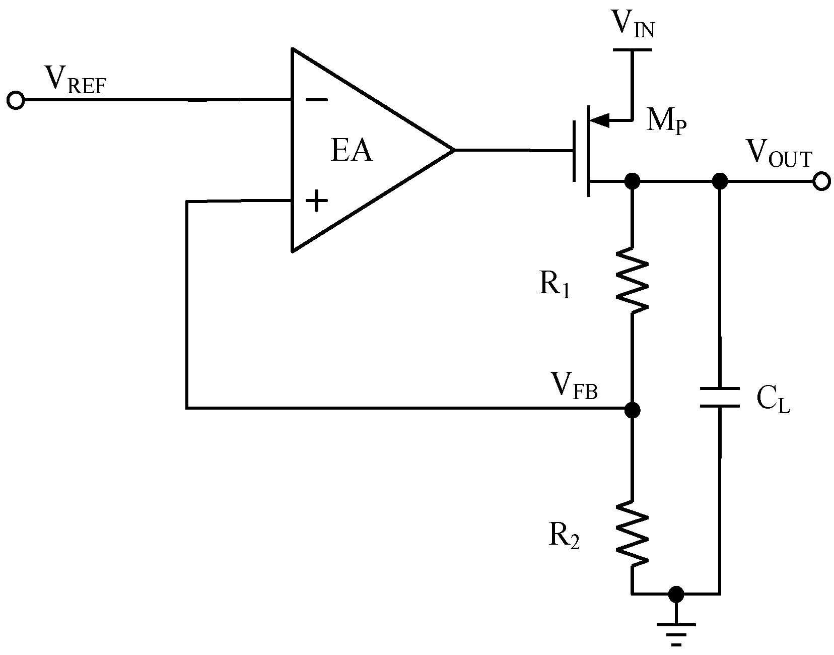
Figure 2.
Basic FVF-based LDO architecture.
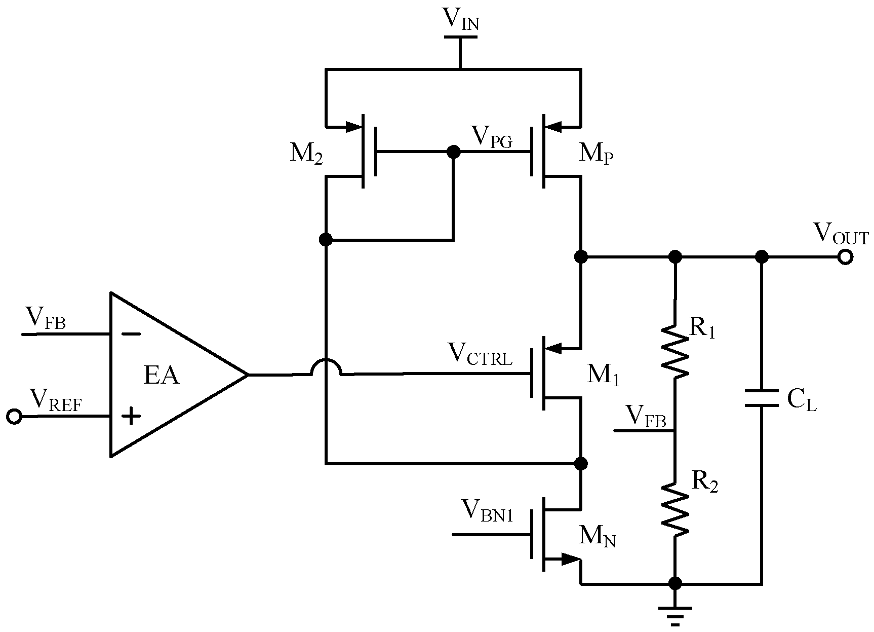
Figure 3.
Block diagram of the proposed LS FVF-based fast-transient LDO.
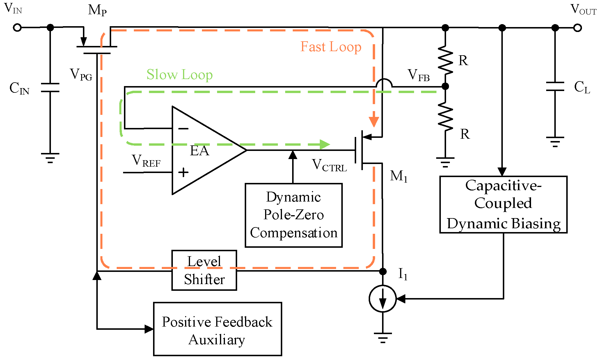
Figure 4.
Schematic of the LS FVF.
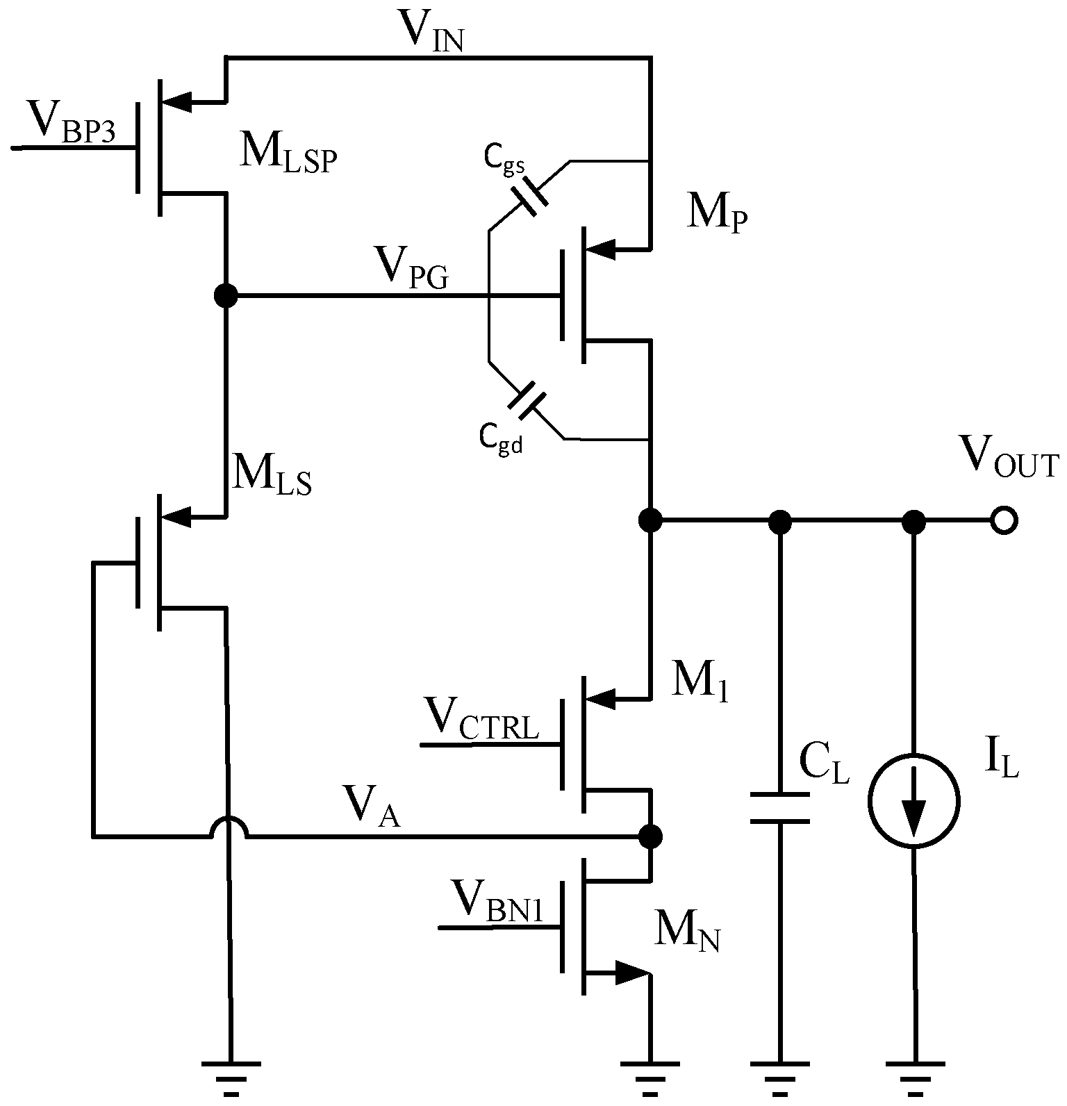
Figure 5.
Schematic of the LS FVF with the Capacitive-Coupled Dynamic Biasing (CCDB) and the Positive Feedback Auxiliary (PFA) circuits.
Figure 5.
Schematic of the LS FVF with the Capacitive-Coupled Dynamic Biasing (CCDB) and the Positive Feedback Auxiliary (PFA) circuits.
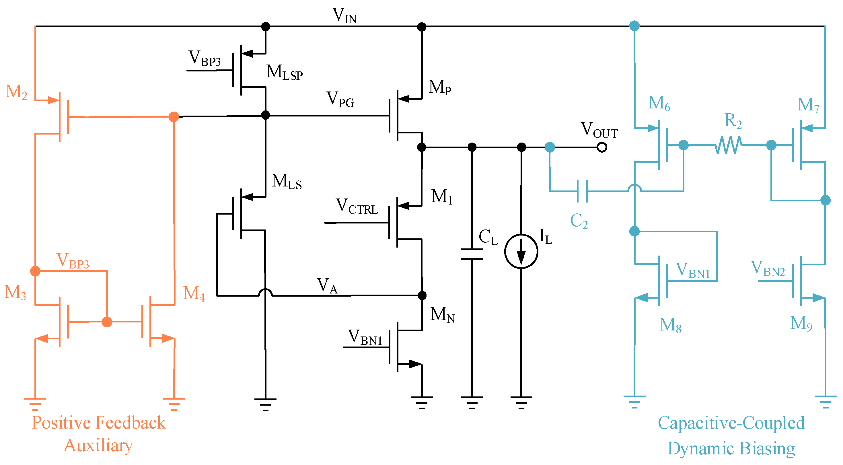
Figure 6.
Load-transient responses of the proposed LDO with and without the CCDB for load-current steps between 0 and 400 mA with a 100-ns transition time.
Figure 6.
Load-transient responses of the proposed LDO with and without the CCDB for load-current steps between 0 and 400 mA with a 100-ns transition time.
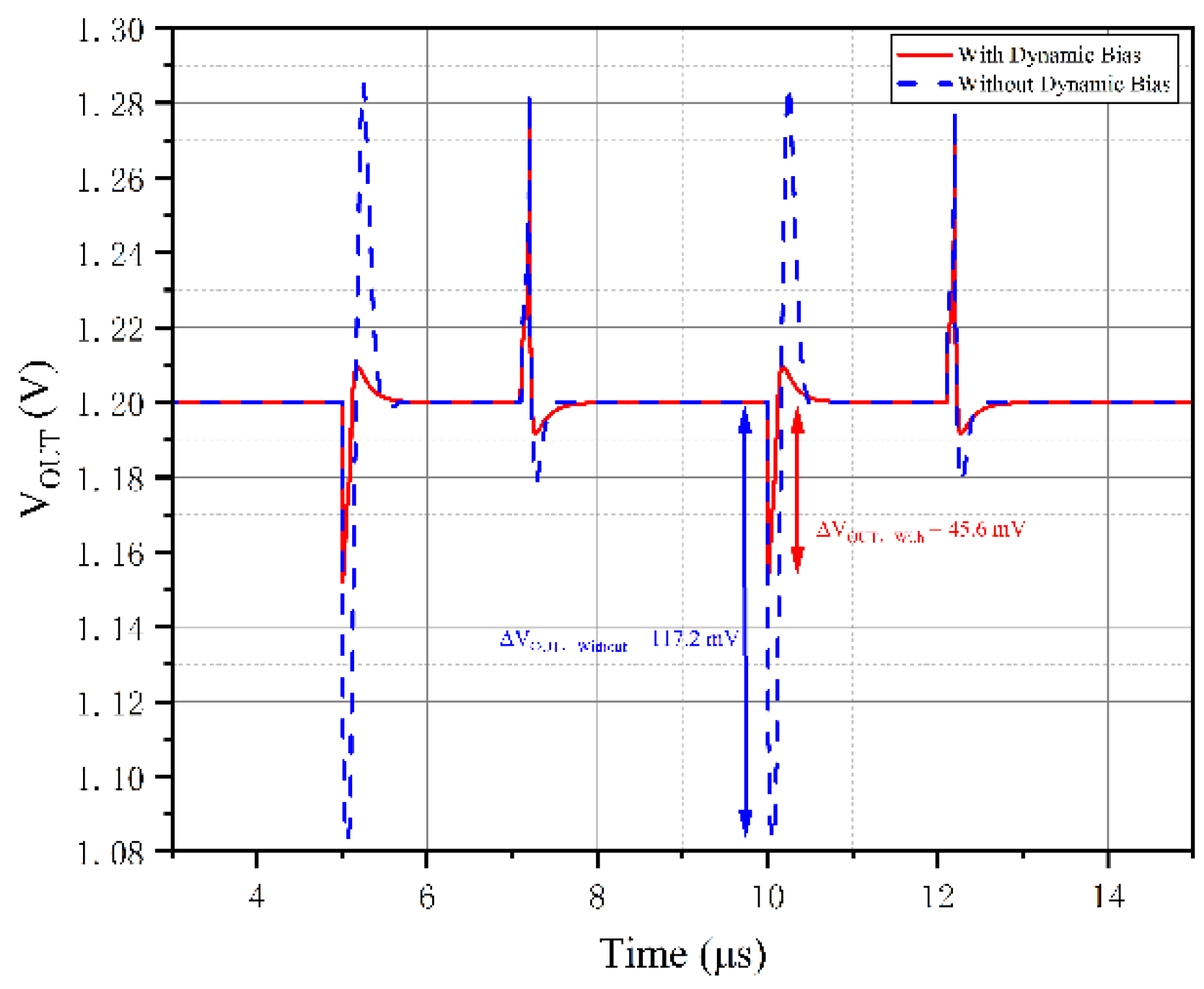
Figure 7.
Load-transient responses of the proposed LDO with and without the PFA for load-current steps between 0 and 400 mA with a 100-ns transition time.
Figure 7.
Load-transient responses of the proposed LDO with and without the PFA for load-current steps between 0 and 400 mA with a 100-ns transition time.
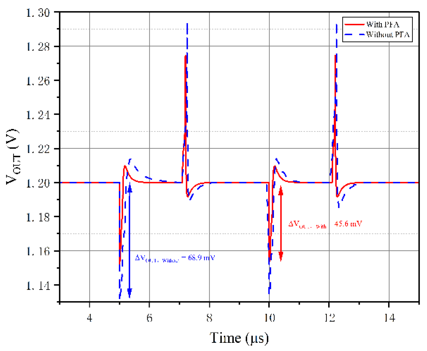
Figure 8.
Schematic of the RFC EA.
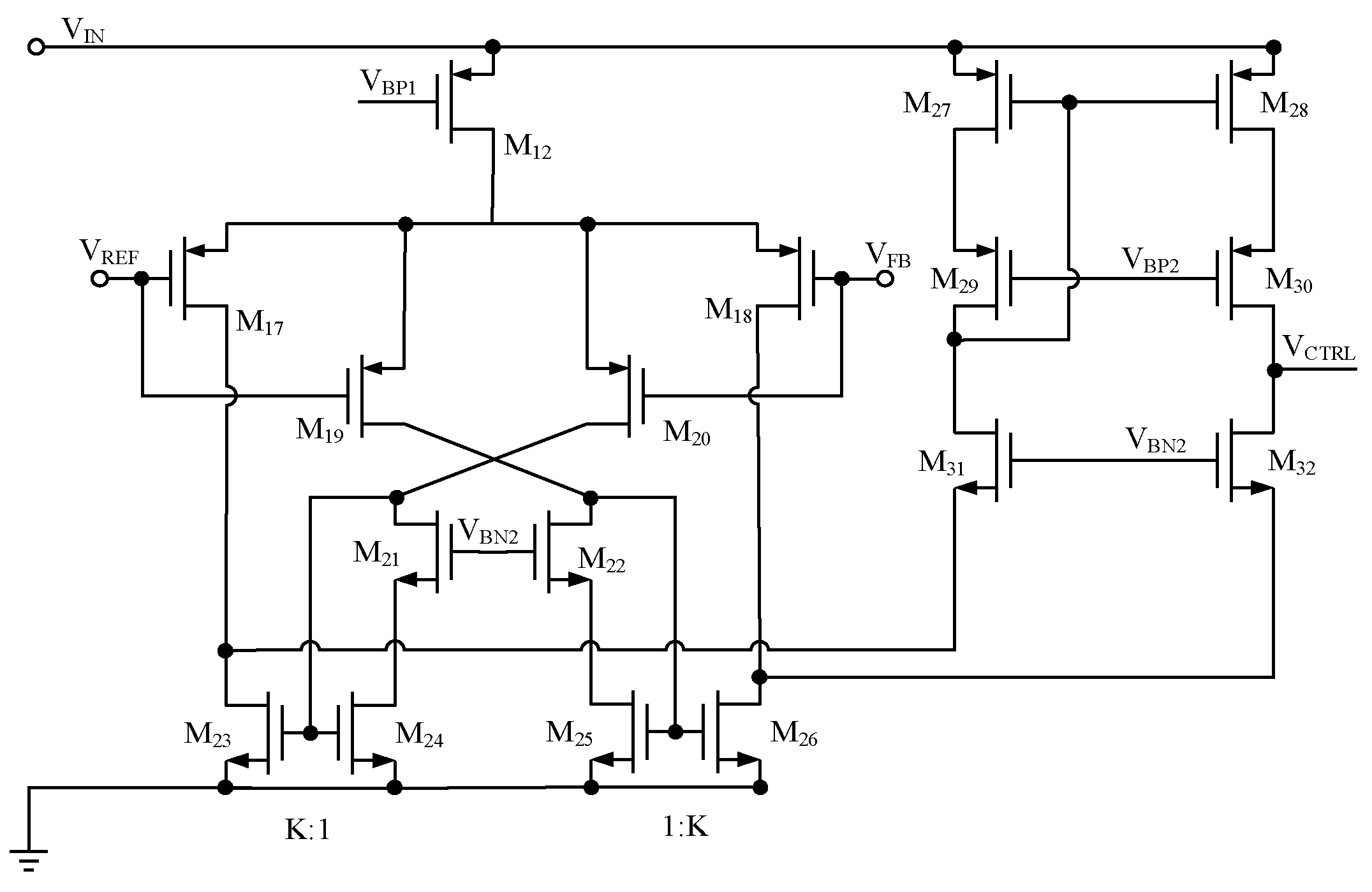
Figure 9.
Gain of the RFC EA.
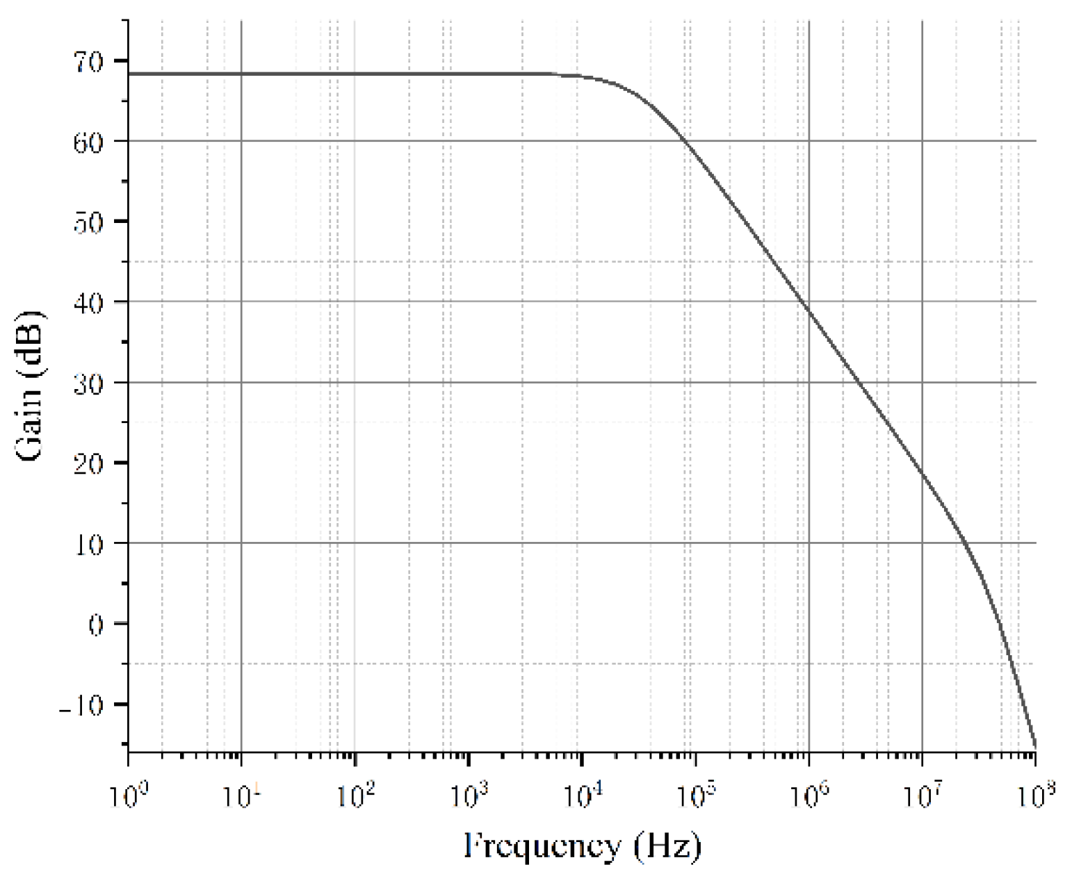
Figure 10.
Schematic of the proposed LS FVF-based fast-transient LDO.
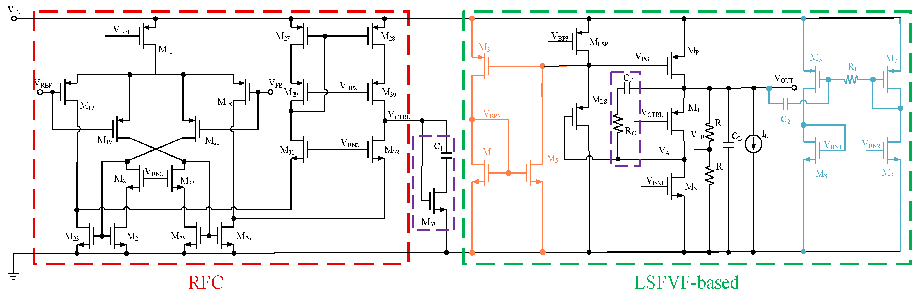
Figure 11.
Small-signal equivalent model of the proposed LDO.
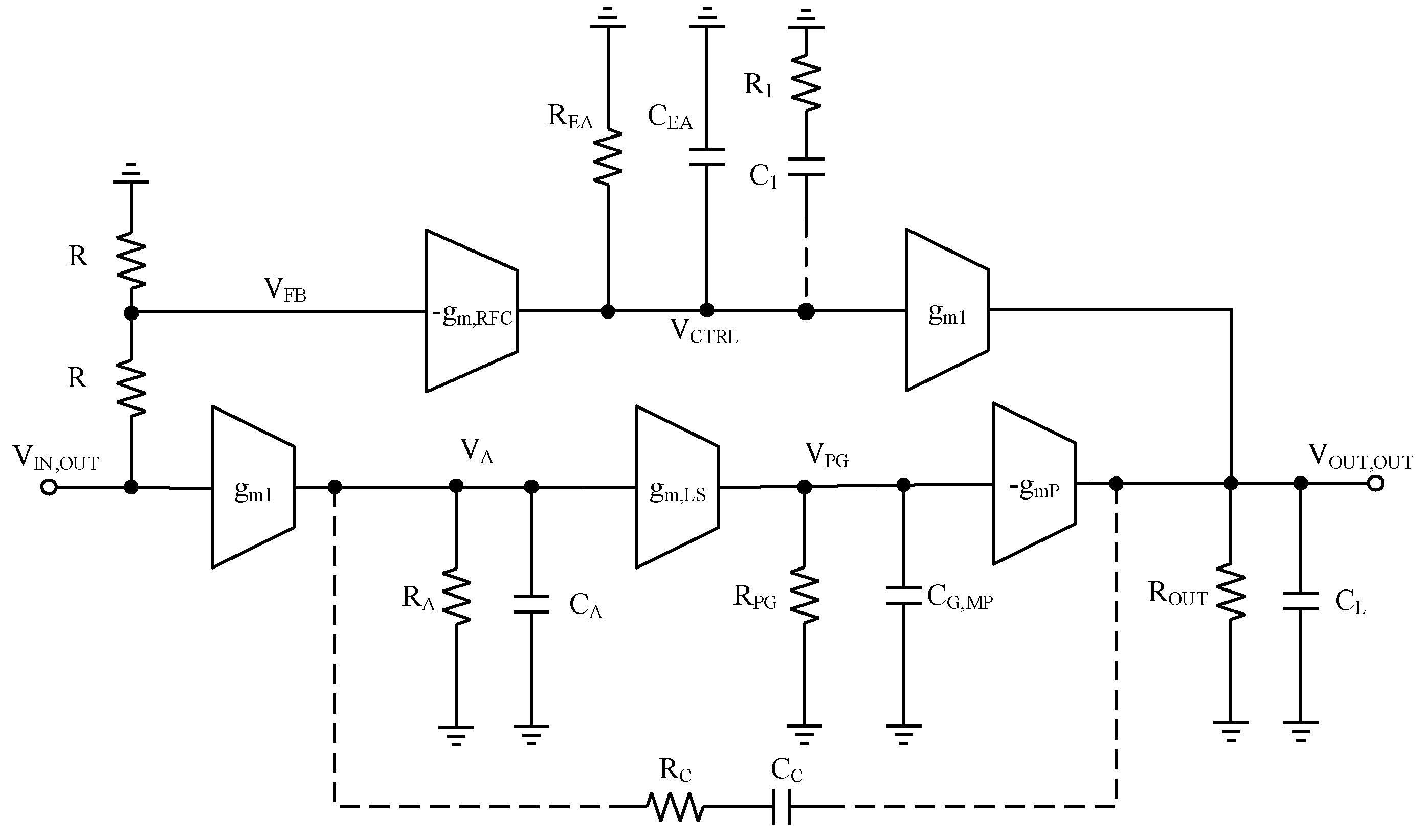
Figure 12.
AC loop-gain and phase under various load currents for the TT corner.
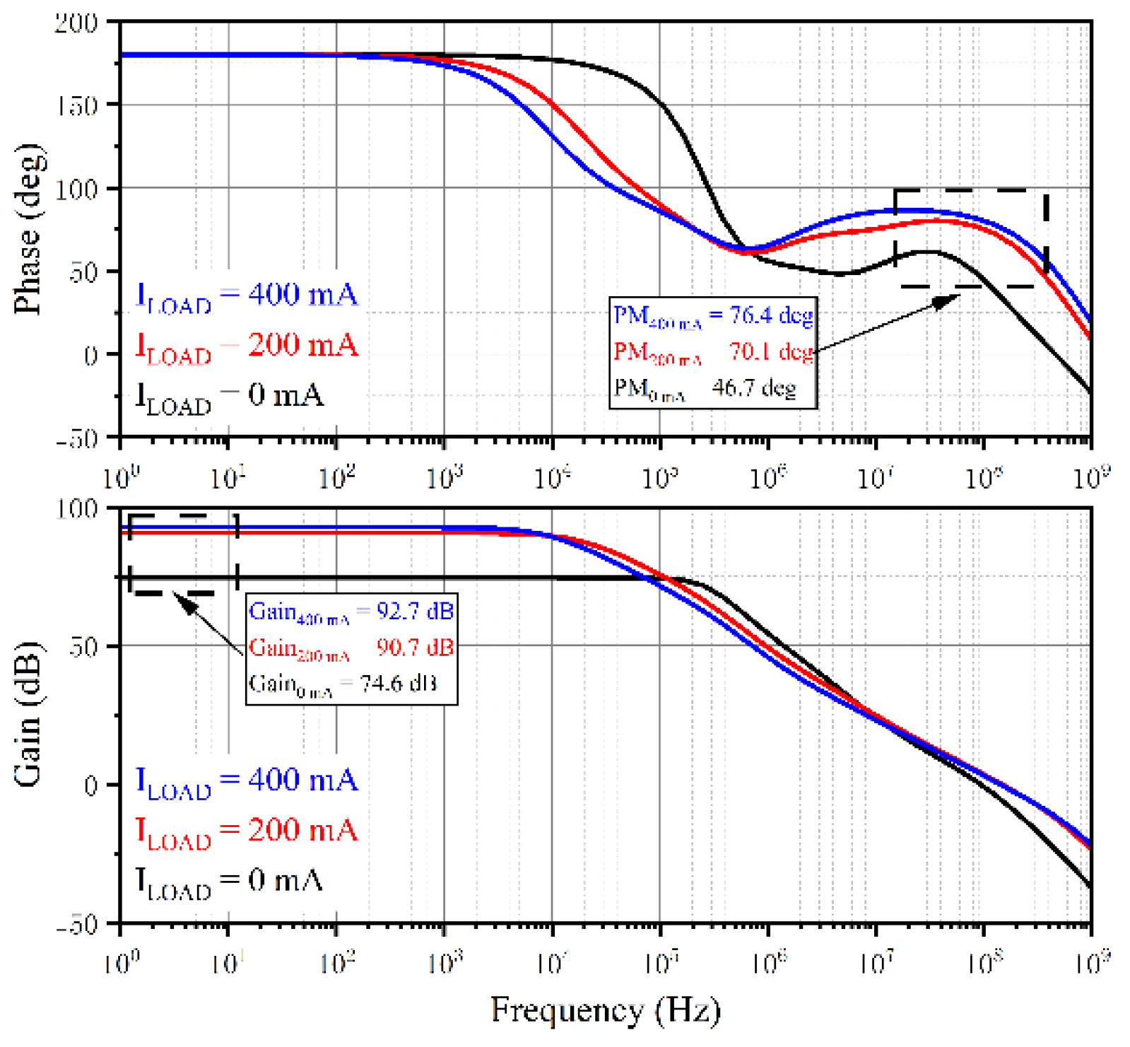
Figure 13.
AC loop-gain and phase under various load currents for (a) the SS corner and (b) the FF corner.
Figure 13.
AC loop-gain and phase under various load currents for (a) the SS corner and (b) the FF corner.
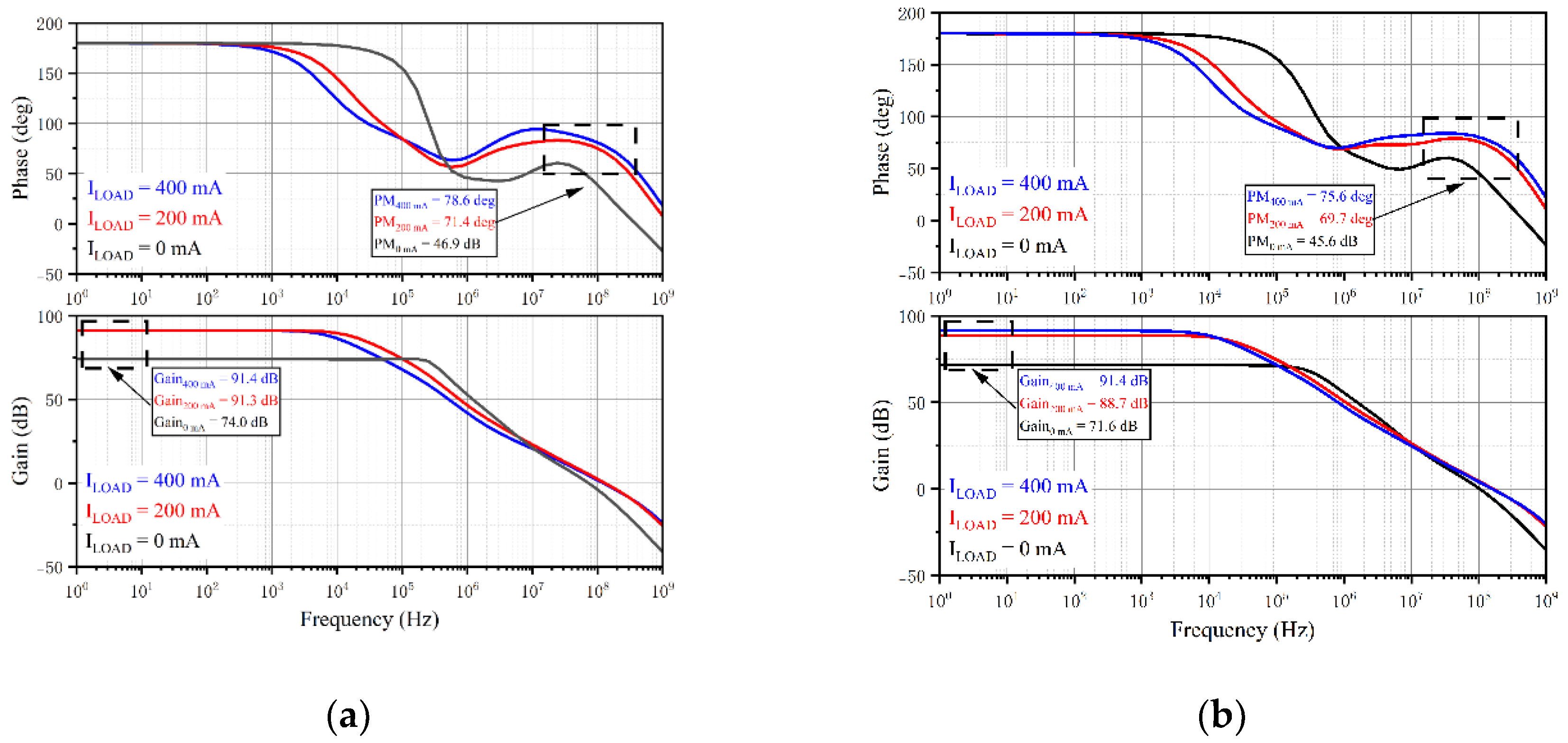
Figure 14.
Layout of the proposed LS FVF-based fast-transient LDO.
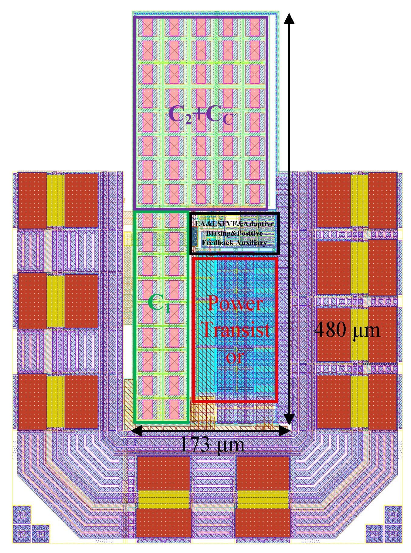
Figure 15.
Transient response of the proposed LDO for load-current steps between 0 and 400 mA with a 100-ns transition time.
Figure 15.
Transient response of the proposed LDO for load-current steps between 0 and 400 mA with a 100-ns transition time.
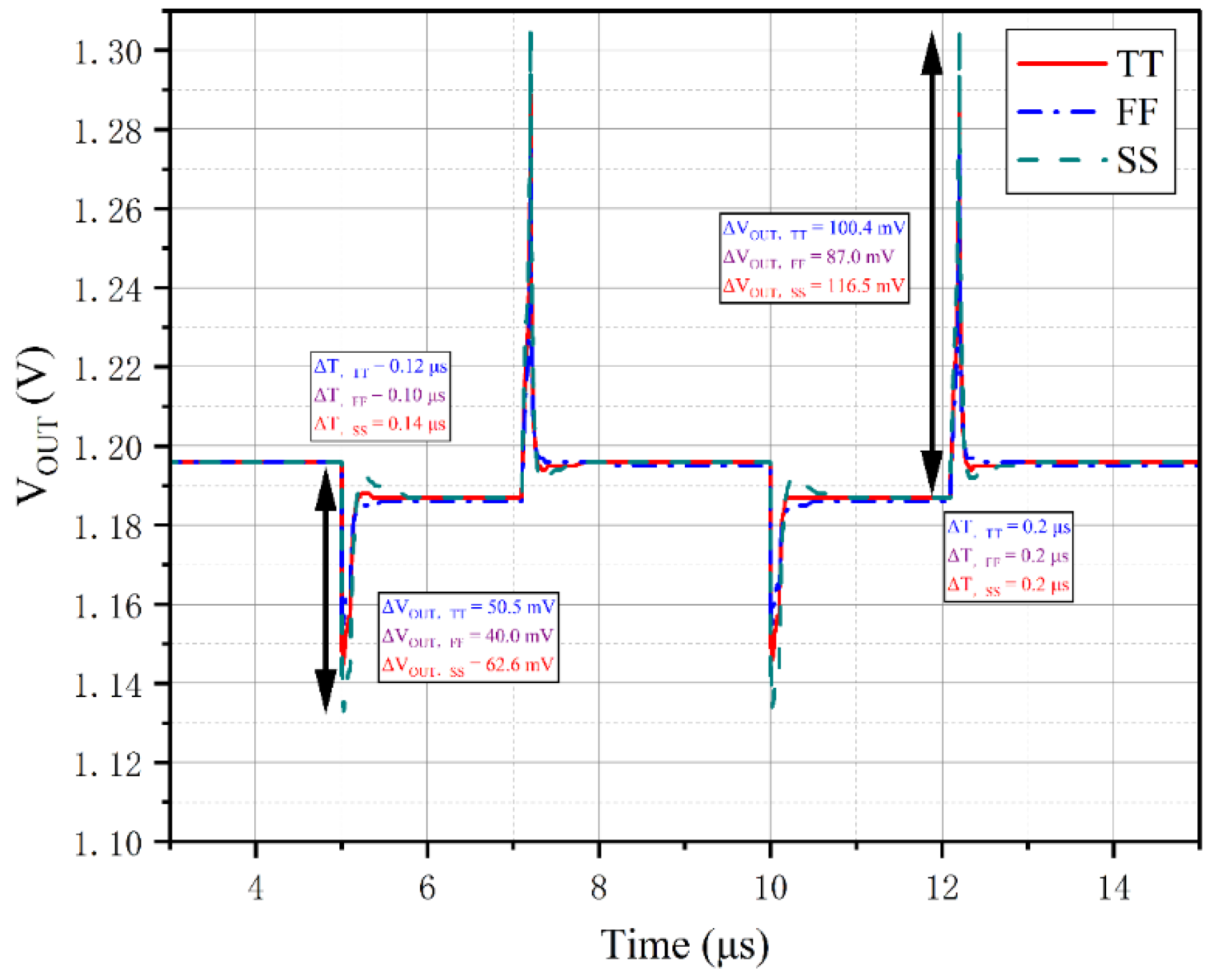
Figure 16.
Line regulation at the TT, FF, and SS process corners with ILOAD = 400 mA.
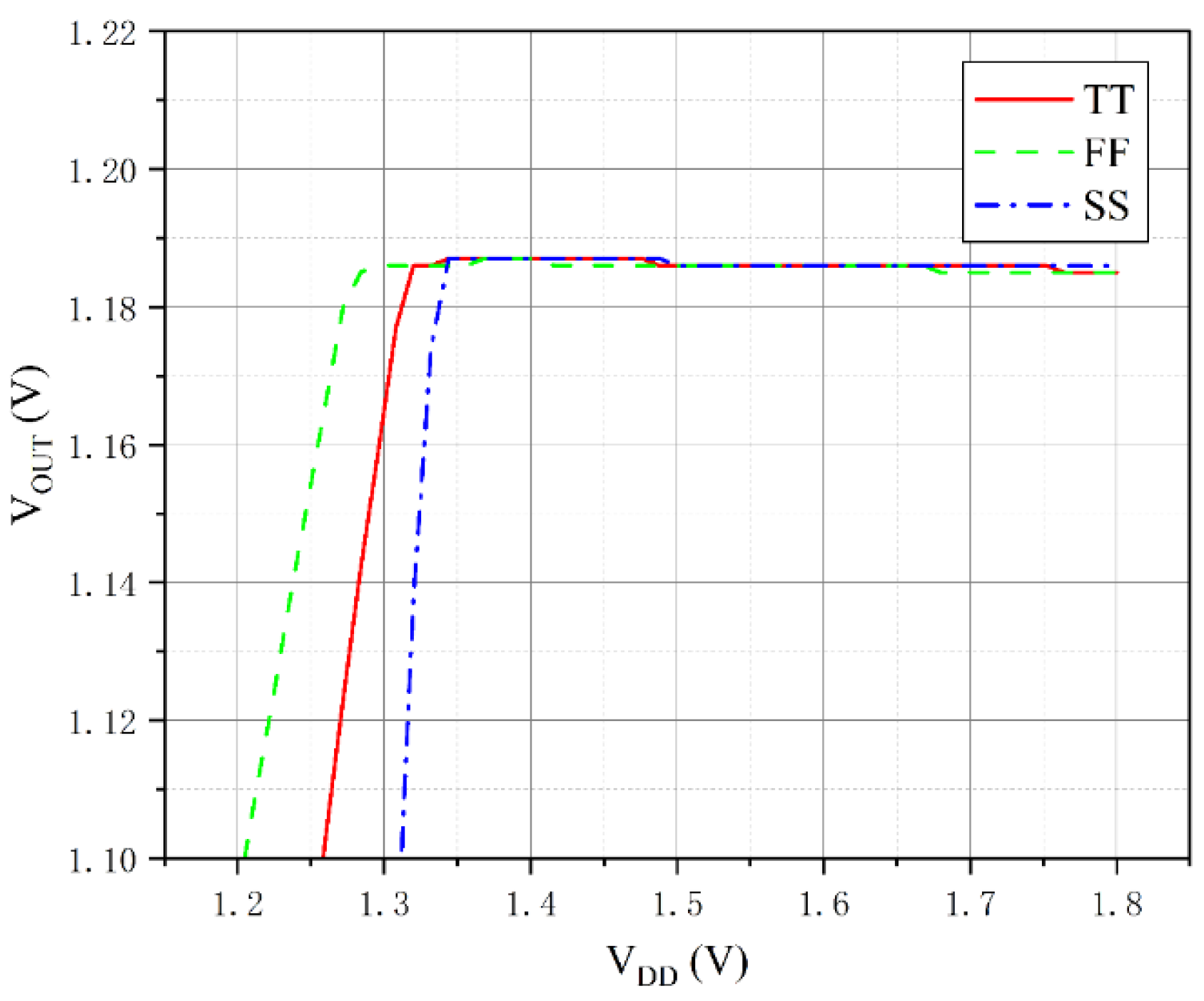
Figure 17.
Load regulation at the TT, FF, and SS process corners.
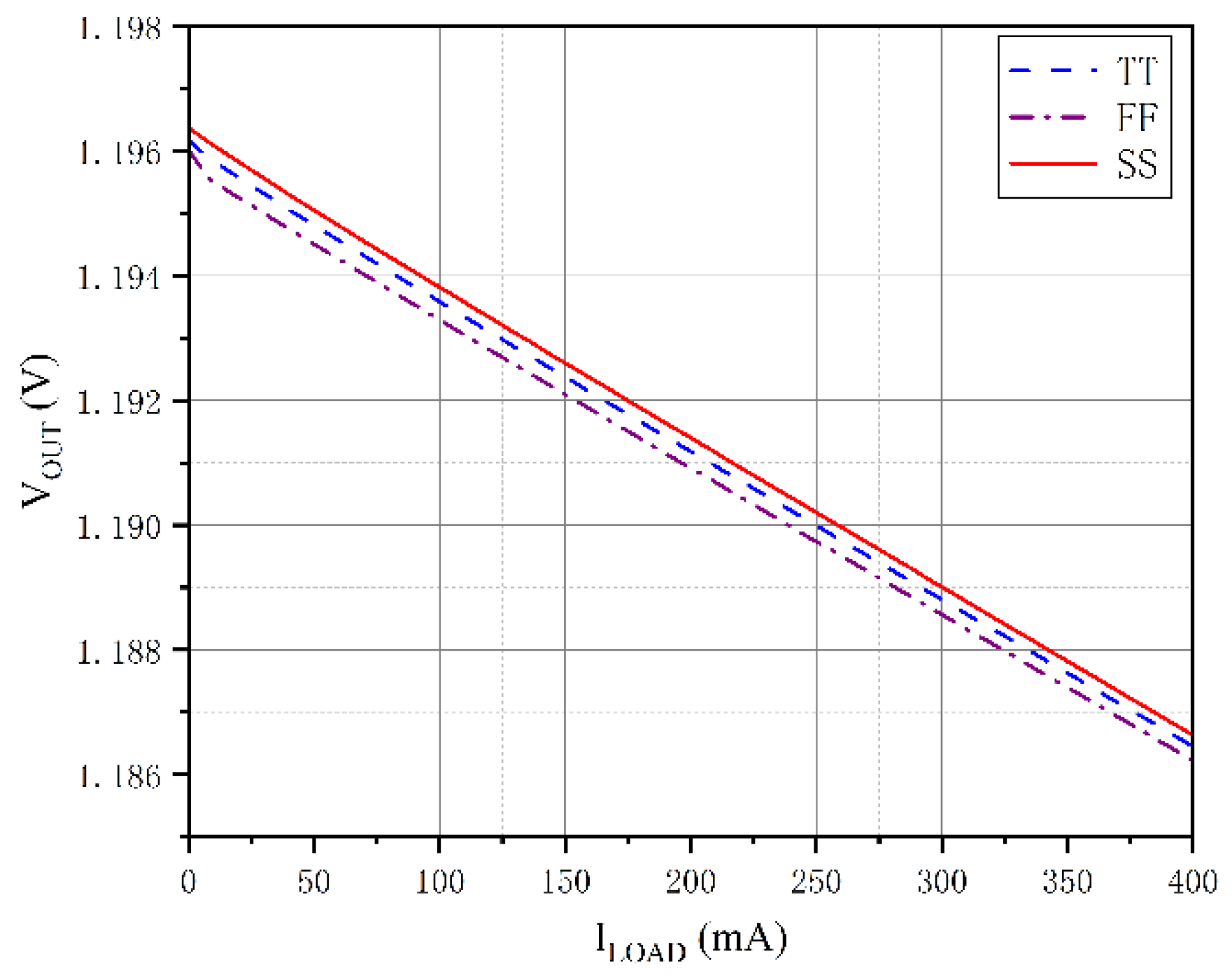
Figure 18.
PSRR versus frequency from 1 Hz to 1 GHz under TT, FF, and SS corners at ILOAD = 400 mA.
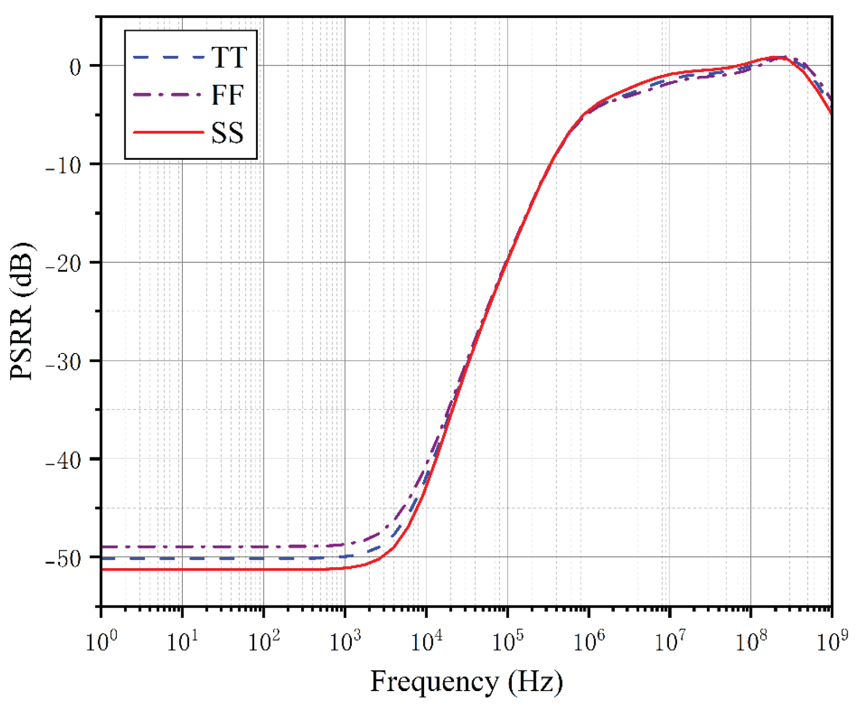

Table 1.
Transient-response parameters at the TT, FF, and SS corners.
| Parameter | TT | FF | SS |
|---|---|---|---|
| Undershoot (mV) | 50.5 | 40.0 | 62.6 |
| Undershoot recovery time (μs) | 0.12 | 0.10 | 0.14 |
| Overshoot (mV) | 100.4 | 87.0 | 116.5 |
| Overshoot recovery time (μs) | 0.2 | 0.2 | 0.2 |
Table 2.
Performance comparison among recent FVF-based LDOs.
| Parameter | [18] | [19] | [21] | [28] | [29] | [30] | This work* |
|---|---|---|---|---|---|---|---|
| Process (nm) | 180 | 90 | 130 | 65 | 180 | 180 | 130 |
| Architecture | FVF + Dynamic Biasing | Push-Pull FVF | FVF + NMCLFT | FVF + SSF | Class-AB SSF | FVF + ELTE buffer | LS FVF + Dynamic Compensation + Dynamic Biasing |
| VIN/VOUT (V) | 1.8/1.0 | 0.9–1.2 / 0.75 | 1.2–1.4 / 1.0 | 1.5 / 1.2 | 2–5 / 1.8 | 1.8–2.3 / 1.6 | 1.5 / 1.2 |
| ILOAD (mA) | 0.1-20 | 0.04-100 | 0-50 | 0-15 | 3-300 | 0-300 | 0-400 |
| CL | 2.8 pF | 100 pF | 0-100 pF | 200 pF | 5 pF | 1 μF | 200 pF |
| Current Efficiency | 99.54% | 99.998% | 99.87% | 99.98% | 99.98% | 99.991% | 99.78% |
| LNR (mV/V) | 0.95 | 0.4 | 48 | - | 0.55 | 2.8 | 2.1 |
| LDR (μV/mA) | 88 | 6 | 6 | - | 1.94 | 62 | 24.3 |
| PSRR | -60.85 dB @ 1 kHz | -51 dB @ 1 kHz | -25 dB @ 1 MHz | -43 dB @ 10 kHz | -60 dB @ 1 kHz | -47 dB @ 100 Hz | -50 dB @ 1 Hz |
| ΔVOUT (mV) | 250 | 350 | 375 | 100 | 86 | 35.8 | 100.4 |
| Recovery time (ns) | 52 | 1200 | 120 | - | 400 | 950 | 200 |
| FOMC (ps) | 0.163 | 0.0056 | 0.945 | 0.21 | 0.0065 | 10.7 | 0.113 |
* The performance parameters of this work are presented at the TT corner unless otherwise specified.
Disclaimer/Publisher’s Note: The statements, opinions and data contained in all publications are solely those of the individual author(s) and contributor(s) and not of MDPI and/or the editor(s). MDPI and/or the editor(s) disclaim responsibility for any injury to people or property resulting from any ideas, methods, instructions or products referred to in the content. |
© 2026 by the authors. Licensee MDPI, Basel, Switzerland. This article is an open access article distributed under the terms and conditions of the Creative Commons Attribution (CC BY) license (http://creativecommons.org/licenses/by/4.0/).
Copyright: This open access article is published under a Creative Commons CC BY 4.0 license, which permit the free download, distribution, and reuse, provided that the author and preprint are cited in any reuse.