

Submitted:
30 July 2026
Posted:
30 July 2026
You are already at the latest version
Abstract
This paper presents an FPGA-based feasibility study of the main digital processing blocks required for future real-time Visible Light Positioning (VLP) receivers. The study focuses on the physical hardware implementation and modular validation of two key components: a Sliding Discrete Fourier Transform (SDFT) pre-processing stage for sinusoidal carrier magnitude extraction and a hardware-optimized Multi-Layer Perceptron (MLP) inference engine for coordinate estimation. The positioning model is trained and evaluated using experimental data acquired from a high-accuracy VLP setup, whereas the FPGA validation is performed at module level on a physical Visible Light Communication (VLC) hardware platform. Therefore, the reported spatial positioning accuracy corresponds to the offline VLP reference dataset, while the FPGA results quantify numerical fidelity, latency, and resource utilization of the implemented hardware blocks. The design was implemented on a Xilinx® Zynq-7000 (xa7z020clg484-1Q) device and operated at 100MHz. The SDFT block requires 61658clock cycles, corresponding to 616.58µs, while the MLP variants require between 606and 6612 clock cycles, corresponding to 6.06µs and 66.12µs, respectively. All MLP implementations reproduce the offline software reference with HW/SW MSE values on the order of 10−6, confirming FPGA numerical fidelity rather than end-to-end positioning accuracy. The results show that the proposed SDFT and MLP hardware blocks constitute viable building blocks for future FPGA-based VLP receivers, while also identifying the remaining integration steps required for a complete end-to-end real-time system.
Keywords:
visible light positioning (VLP)
; FPGA
; sliding DFT (SDFT)
; artificial neural network (ANN)
; hardware acceleration
; fixed-point arithmetic
1. Introduction
The widespread deployment of LED lighting infrastructure has positioned Visible Light Positioning (VLP) as a promising and cost-effective alternative to traditional RF-based systems for indoor localization. VLP offers inherent advantages such as enhanced security, immunity to electromagnetic interference, and the potential to achieve centimeter- or even millimeter-level accuracy, making it particularly attractive for applications including industrial automation, autonomous robotics, warehouse logistics, and human–machine interaction in smart environments [1,2]. In these application scenarios, the demand for high-accuracy and low-latency indoor positioning has increased significantly, with systems required to operate under strict timing constraints and limited computational and hardware resources [1,3,4,5]. These requirements are especially relevant in Industry 4.0 and robotic applications, where deterministic processing and low-complexity embedded implementations are necessary.
VLP systems are broadly categorized according to the receiver type: Image Sensor-based (IS-based) and Photodiode-based (PD-based). IS-based systems can achieve high accuracy by exploiting imaging information and Angle of Arrival (AoA) processing, but their computational burden and frame-processing latency can restrict real-time deployment on embedded platforms. Reported IS-based systems exhibit positioning delays around to [5,6]. Furthermore, the use of Artificial Neural Networks (ANNs) with imaging receivers can achieve high positioning accuracy, but it requires processing pipelines that must be carefully adapted before being deployed in embedded hardware [7]. In contrast, PD-based VLP relies on Received Signal Strength (RSS) or frequency-domain processing, offering simpler front-end hardware, although RSS-based approaches can be sensitive to non-line-of-sight effects and may require computationally demanding channel models [1].
Frequency-domain VLP based on Frequency Division Multiplexing (FDM) provides a practical alternative, since multiple LEDs can transmit sinusoidal signals at distinct carrier frequencies. Dedicated hardware has already been used in frequency-based VLP, with reported position errors within 7 cm [2]. In parallel, machine learning and fingerprinting methods have been used to model the nonlinear relationship between measured signal features and position, with approaches such as Extreme Learning Machine (ELM) providing high-speed and accurate localization [8]. However, moving these methods from offline or processor-based evaluation to FPGA-based execution requires a careful analysis of arithmetic precision, latency, memory usage, and resource consumption.
Despite these advances, there remains a practical gap between high-accuracy VLP demonstrations and the hardware implementation of the main processing blocks required to build compact real-time receivers. In particular, a receiver that combines continuous spectral extraction and neural-network inference must be evaluated by distinguishing the offline spatial-positioning baseline from the FPGA numerical fidelity, resource utilization, and module-level hardware latency of the implemented processing blocks. This work addresses that gap from a hardware-oriented perspective.
This work does not claim a complete end-to-end real-time VLP demonstrator. Instead, it evaluates the FPGA feasibility of the main processing blocks required to build such a receiver. The study focuses on the physical implementation and modular validation of an SDFT pre-processing block and several MLP inference-engine architectures on a low-cost Xilinx® Zynq-7000 FPGA. The offline spatial-positioning baseline is obtained from experimental data acquired with a high-accuracy VLP setup [7], whereas the FPGA validation quantifies HW/SW numerical agreement, resource utilization, and module-level hardware latency of the implemented SDFT and MLP blocks.
The main contributions of this work are summarized as follows:
- 1.
- A modular FPGA-oriented architecture is proposed for future VLP receivers combining SDFT-based spectral pre-processing and MLP-based coordinate estimation.
- 2.
- The SDFT block is physically implemented and evaluated on FPGA for the extraction of sinusoidal carrier magnitudes, using the carrier set , , , and .
- 3.
- Four MLP inference-engine architectures are implemented and compared on FPGA: sequential accumulation, floating-point tree reduction, fixed-point tree reduction, and a BLAS-based implementation.
- 4.
- A module-level hardware analysis is provided in terms of latency, resource utilization, arithmetic precision, and numerical fidelity with respect to the offline software reference model.
- 5.
- The feasibility and limitations of sequential and projected parallel architectures are discussed, clarifying the remaining steps required to reach a complete end-to-end real-time VLP receiver.
2. Related Work and Scope of Contribution
Existing VLP systems differ significantly in receiver type, positioning algorithm, hardware platform, and degree of real-time integration. IS-based systems can provide high spatial-positioning accuracy but generally require image processing stages whose latency and computational complexity can be high for embedded applications [5,6]. PD-based and FDM-based systems reduce front-end complexity and are more naturally aligned with digital signal-processing hardware [1,2]. Machine-learning approaches, including ANN- and ELM-based localization, can improve the offline or processor-based mapping from measured signal features to spatial coordinates. However, their deployment on resource-constrained devices requires dedicated hardware analysis [7,8].
Table 1 summarizes the positioning of this work using only the information available in the cited works included in the manuscript. The purpose of the comparison is not to claim end-to-end superiority, but to clarify the specific contribution of the present study: modular physical FPGA validation of the SDFT and MLP processing blocks needed for future real-time VLP receivers.
As shown in Table 1, previous systems demonstrate either end-to-end VLP operation using processor-based or PC-assisted processing, or high-accuracy offline positioning based on imaging-MIMO and ANN models. However, the FPGA implementation of the spectral extraction and neural inference blocks required to migrate such offline processing chains toward embedded receivers remains insufficiently characterized. This paper addresses this specific hardware-oriented gap.
3. Experimental Setup and Validation Scope
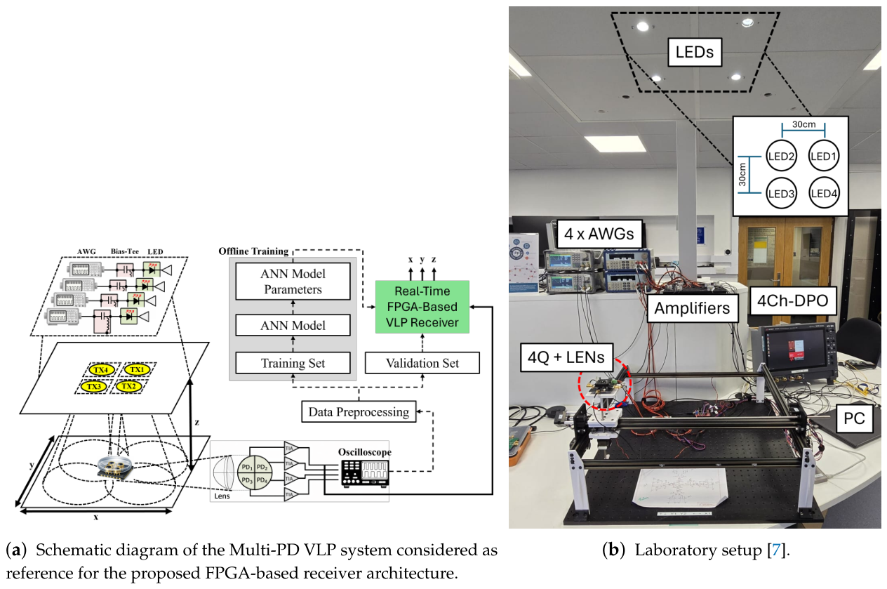
The experimental basis of this work consists of two distinct elements that must be clearly separated: the VLP dataset used to train and evaluate the positioning model (Figure 1), and the physical FPGA/VLC platform used to validate the hardware implementation of the digital processing blocks (Figure 2). This separation is central to the scope of the paper. The work evaluates the feasibility of the SDFT and MLP hardware modules; it does not implement a complete end-to-end real-time VLP system.
3.1. Reference VLP Dataset and Offline Positioning Baseline
The data used for training and offline evaluation of the positioning model were collected using the laboratory setup described in the high-accuracy VLP system (Figure 1) reported in [7]. This setup provides real experimental VLP data and is used in this work as the reference source for the localization model and the offline spatial-positioning baseline.
3.2. Transmitter Configuration and Signal Modulation
The transmitter array and signal modulation protocols for data generation were kept consistent with the reference work [7]. The setup consists of four symmetrically distributed LED transmitters (TXs) serving simultaneously as illumination sources and signal beacons. The system employs a 2 × 2 array of four TXs, spaced 300 mm apart in a square configuration, as shown in Figure 1(b). Each transmitter unit uses a Samsung LM561C LED combined with an LEDiL EMILY-W reflector, which constrains the light output to a beam divergence of 40°. Each LED is biased with an average current of 75 mA, resulting in a luminous flux of 46 lumens.
The modulation is generated by four Arbitrary Waveform Generators (AWGs), which produce distinct sinusoidal modulating signals for the four channels. To satisfy the non-negative optical-intensity requirement of Intensity Modulation/Direct Detection (IM/DD), these sinusoidal signals are converted into unipolar signals by adding a DC voltage through Bias-Tees (MINI-CIRCUITS, ZFBT-4R2GW-FT+) before driving the LEDs. This frequency-separated transmission structure provides the basis for the SDFT-based spectral feature extraction considered in the proposed hardware architecture.
3.3. Receiver Hardware and Data Collection
The raw analog data streams used to train the MLP algorithm were captured using the high-sensitivity receiver chain described in [7]. The receiver uses a plano-convex aspheric singlet lens (THORLABS, ACL2520U) with a diameter of 25 mm and a focal length of 20.1 mm. A four-element Photodiode (PD) array acts as the detector. A focal offset is used to obtain a Field-of-View (FoV) of 37.5°, which closely matches the transmitter beam divergence. Each PD output is processed by a Trans-Impedance Amplifier (TIA) (MAX3665) and then by a Low-Noise Amplifier (LNA) with 20 dB gain (MINI-CIRCUITS, ZFL-1000LN+).
The four amplified analog signals were digitized and captured using a four-channel digital oscilloscope, forming the dataset used for offline MLP training and for defining the offline spatial-positioning baseline. In the future complete receiver, this acquisition stage would be replaced by an ADC interface connected to the FPGA. In the present work, however, the ADC-to-position end-to-end chain is not experimentally implemented; instead, the available dataset is used as a reference for the hardware-level verification of the MLP inference engine.
3.4. FPGA Hardware Validation Platform
The physical hardware validation of the implemented SDFT and MLP modules was performed using the existing VLC system (Figure 2) described in [9,10]. This platform provides an optical link and an FPGA-based processing environment in which the digital modules can be implemented and evaluated under controlled conditions. The system includes two optical links, one in the visible spectrum and one in the infrared; in this work, only the visible link is used.
The system is based on an XA Zynq-7000 (xa7z020clg484-1Q) SoC FPGA [11]. The platform integrates ECS-TXO-2016 oscillators running at 40 MHz to provide stable clock signals for the Digital-to-Analog Converter (DAC) and Analog-to-Digital Converter (ADC), ensuring timing alignment with the digital hardware. The visible optical link uses OSRAM LUW CN7N ultra-white LEDs driven through an SMA interface. A Ledil F15558 MIRELLA-G2-S reflector shapes the emitted beam. On the receiver side, an OSRAM BP 104 S photodetector with an active area of 4.84 mm2 is used together with a Fresnel lens of 15 mm diameter and 10 mm focal length. The received optical signal, with a measured bandwidth of approximately 9.15 MHz, is amplified before being processed by the FPGA.
3.5. Scope of Validation
The validation presented in this paper is modular. The SDFT module is physically validated through the visible optical link by processing one sinusoidal carrier at a time. This confirms the hardware capability to extract individual target tones, but it does not demonstrate simultaneous separation of the four carriers under the full VLP operating scenario. The MLP module is physically implemented on the FPGA and validated numerically against the offline software reference model using data derived from the experimental VLP dataset. Therefore, the reported MLP MSE values quantify FPGA HW/SW numerical fidelity, not end-to-end real-time positioning accuracy.
4. Proposed FPGA-Oriented Receiver Architecture
The proposed architecture (Figure 3) targets the migration of an offline VLP processing chain toward an embedded FPGA implementation. Conceptually, the future receiver would acquire the amplified PD signals through ADCs, perform spectral extraction using SDFT, and execute MLP inference to estimate the spatial coordinates. In this paper, the SDFT and MLP blocks are implemented and validated as physical FPGA modules, while the complete ADC-to-coordinate VLP receiver remains a future integration step.
The physically feasible implementation on the target XA Zynq-7000 device is a sequential, or time-multiplexed, architecture. In this configuration, a single SDFT module is reused to process the receiver channels sequentially under the control of a dedicated control unit. This approach reduces resource utilization and allows the SDFT and MLP modules to fit within the constraints of the low-cost FPGA platform. The architecture implemented and evaluated on the Zynq-7000 must therefore be interpreted as a modular sequential implementation of the main processing blocks, not as four independent SDFT channels operating concurrently in the final physical design.
A fully parallel architecture with four independent SDFT modules remains relevant as a scalability option for larger FPGA devices. In such a projected architecture, each PD channel could be assigned a dedicated SDFT processing path, reducing the total processing latency at the expense of substantially higher resource utilization. The parallel architecture is therefore discussed only as a projected alternative for devices with more resources, such as the AMD Zynq™ UltraScale+™MPSoC ZCU104, and not as the architecture physically validated on the low-cost Zynq-7000 platform.
4.1. Sliding DFT Pre-Processing
The SDFT is used to extract the magnitudes of the sinusoidal carrier frequencies associated with the VLP transmission scheme. The recursive SDFT update for the k-th frequency bin is defined as [12]
Here, is the updated spectral component, is the previous spectral component, is the newest sample entering the window, and is the oldest sample leaving the window. This recursive structure reduces the computational cost associated with repeated full FFT calculations and is therefore suitable for FPGA-based spectral tracking.
The determination of the SDFT parameters—namely, the window size N and the sampling frequency —is critical for achieving the required frequency resolution while maintaining signal integrity for the localization engine. The proposed VLP system employs four distinct sinusoidal carrier frequencies, namely , , , and . After iterative analysis, an SDFT window size of was selected, as it provides sufficient spectral resolution to accurately isolate the 200 kHz spacing between adjacent channels.
From a theoretical perspective, the frequency resolution of the SDFT is determined by both the window size N and the sampling frequency , and is given by Equation (2).
In the proposed hardware implementation, the sampling frequency is fixed by the ADC characteristics and FPGA clocking constraints. To satisfy the Nyquist–Shannon sampling theorem for the highest carrier frequency () while providing robust oversampling, a sampling frequency of was selected. This rate is generated by a dedicated VHDL-based sampler core that provides a stable and synchronized data stream for the SDFT processing stage. In the Zynq-7000 implementation, the SDFT core is reused sequentially across receiver channels, whereas a parallel multi-SDFT configuration is considered only as a scalability option for larger devices.
Under these fixed sampling conditions, increasing the window size N directly improves the frequency resolution, enabling more accurate isolation of the target carrier frequencies. Beyond spectral resolution, a larger window size also enhances the effective signal-to-noise ratio (SNR) of the detected frequency components, as the SDFT coherently integrates signal energy over a longer observation interval while averaging out uncorrelated noise. This improvement in SNR results in more stable and repeatable magnitude estimates at the SDFT output.
These more reliable magnitude estimates directly benefit the downstream MLP inference engine by reducing variance in the input feature vector, which in turn improves the robustness and accuracy of the resulting 2D position estimates. Consequently, the selection of represents a balanced trade-off between frequency resolution, SNR enhancement, and hardware latency, achieving reliable separation of the 200 kHz-spaced carriers while maintaining real-time performance and low computational complexity suitable for FPGA implementation.
The physical FPGA validation of the SDFT block reported in this paper verifies the extraction of individual carrier tones over the visible optical link. It does not experimentally validate simultaneous four-tone separation under full VLP conditions, including cross-channel interference, unequal received powers, multipath, or complete optical front-end integration. This limitation is explicitly considered in the interpretation of the results.
4.2. MLP Inference Engine
The MLP maps the spectral features derived from the receiver channels to the estimated 2D coordinates . The input vector has 16 components, corresponding to four receiver channels and four carrier-frequency magnitudes per channel. The network topology consists of an input layer with 16 inputs, two hidden layers with 32 neurons each, and an output layer with two neurons. The two hidden layers use the hyperbolic tangent sigmoid activation function, while the output layer uses a linear activation function. This specific MLP topology follows the offline-trained reference model used to obtain the spatial-positioning baseline reported in [7].
The network structure is expressed as
- Input layer: ,
- First hidden layer: , , hyperbolic tangent sigmoid activation,
- Second hidden layer: , , hyperbolic tangent sigmoid activation,
- Output layer: , , linear activation.
The forward propagation is given by
where denotes the hyperbolic tangent sigmoid activation function and is the coordinate output.
The MLP parameters, including weights and biases, are stored in external memory for easy updates through the FPGA’s processor system (PS). The MLP Inference Engine can load these parameters into on-chip BRAM within the programmable logic (PL) to minimize latency and enhance inference performance. At module level, the implemented MLP inference engine removes the need for software-based neural-network inference and provides a low-latency hardware block suitable for integration into future real-time VLP receivers.
The MLP is trained and evaluated offline using the experimental VLP dataset. The FPGA implementation is then validated by comparing the hardware output against the software reference output. Consequently, the MSE values reported for the MLP quantify numerical agreement between the FPGA inference engine and the offline model, not a new physical measurement of real-time positioning accuracy.
5. Hardware Implementation and Optimization
For the hardware implementation, the proposed workflow illustrated in Figure 4 was followed. This workflow, introduced by the authors, is specifically designed for integration within the Xilinx® development environment. The first step consists of developing a software model to serve as a reference for the hardware implementation. In this work, a Python model of the SDFT algorithm was implemented and tested using several parameter combinations to ensure compliance with the system requirements.
In parallel, a MATLAB® model of the neural network was developed to simulate the complete processing flow. For this purpose, 10000 samples of 1024 points per channel were collected using an oscilloscope. These data were processed with an FFT to extract the relevant frequency tones. Subsequently, 80% of the dataset was employed to train the neural network (NN), while the remaining 20% was reserved for validation.
Using this golden dataset, the hardware implementation of the corresponding modules (SDFT and MLP ANN) was carried out in Xilinx® Vitis™ HLS. This methodology was selected to accelerate development time and simplify the testing process. The resulting Register Transfer Logic (RTL) IP cores were exported to the Vivado™ IP Integrator tool to construct the hardware platform. Finally, the software platform was created in Xilinx® Vitis™ to control and manage the hardware implementation through the PS embedded in the SoC FPGA.
5.1. SDFT Hardware Architecture
Figure 5 illustrates the proposed architecture for the hardware implementation of the SDFT. The design requires an initial 64-point FFT operation, which is implemented using the Xilinx® Fast Fourier Transform v9.1 LogiCORE [13], and configured with a window size of 64 and a fixed-point data type of ap_fixed〈32,1〉 (with 32 total bits and 1 bit allocated to the integer part). However, since the received signal exhibits a wide dynamic range, a fixed-point representation of ap_fixed〈39,9〉 is adopted for the interface, complemented by a scaling stage to ensure the numerical stability and numerical fidelity of the FFT operation.
For the sliding component of the algorithm, a multiplication by is required. Since computing this exponential function directly in the hardware is computationally expensive, a lookup table (LUT) is used to store the precomputed values of this function, with k used as the index. This approach significantly reduces latency. In addition, a shift register is implemented to manage the generation of the input samples and , ensuring the correct sequencing of data for the SDFT operation.
In order to obtain the magnitude of each frequency bin, the complex absolute value must be computed. For a complex number , the exact magnitude is defined as:
As shown in Equation (6), this operation requires both a squaring and a square root, which are computationally expensive in hardware implementations, particularly for FPGA or ASIC designs where latency and logic resources are critical constraints. To address this issue, several approximation methods have been proposed in the literature to replace the exact computation of the magnitude with simpler arithmetic operations while maintaining acceptable accuracy.
A widely adopted family of methods expresses the magnitude as a weighted sum of the maximum and minimum of the absolute values of the real and imaginary parts, namely
where the constants and are selected to minimize the approximation error. For example, the approximation provides a good trade-off between accuracy and complexity [14]. More refined coefficients, such as and , have been reported to reduce the maximum error to below 4% [15].
In this work, such an approximation is employed to enhance the hardware efficiency of the magnitude calculation, thereby reducing both latency and resource utilization while maintaining the precision required for the system. In particular, the method proposed in [14] is adopted, as it eliminates the need for multipliers by replacing them with a simple one-bit right shift operation, further optimizing the implementation for FPGA-based architectures.
5.2. MLP Core Design and Pipelining
For the MLP core, four different implementations were developed to analyze their impact on performance and resource utilization. High-Level Synthesis (HLS) was employed to accelerate development and testing, as it significantly reduces design time compared to traditional RTL approaches. Moreover, based on the authors’ experience, HLS is particularly well-suited for this type of algorithm due to its efficient mapping of matrix–vector operations onto FPGA resources.
In order to evaluate different design trade-offs, four implementations of the MLP core were developed and synthesized on the FPGA:
- Sequential accumulator: A straightforward implementation where the multiply–accumulate (MAC) operations are executed sequentially. This version minimizes resource usage and serves as a baseline to compare the performance and resource consumption of the optimized designs.
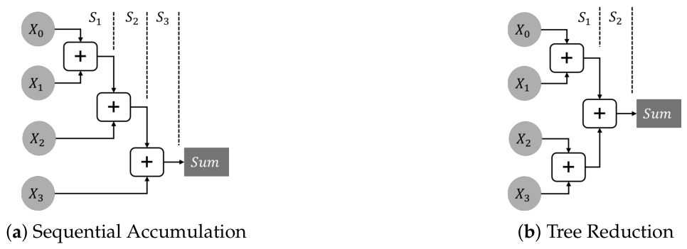
- Tree reduction (floating-point): In this approach, the summation of products is parallelized using a tree reduction algorithm, which organizes the partial sums in a binary tree structure [16]. Instead of adding all terms sequentially, pairs of terms are summed in parallel and then recursively reduced until the final result is obtained. This reduces the overall latency from to additions, significantly improving performance while maintaining floating-point precision [17,18]. Figure 6 illustrates the difference between sequential accumulation and tree reduction for summing four elements.
- Tree reduction (fixed-point,ap_fixed〈24,10〉): Similar to the previous method, but using fixed-point arithmetic with a word length of 24 bits and 10 integer bits [19]. This representation balances numerical precision with reduced hardware cost, leading to lower resource utilization and latency compared to floating-point implementations, while preserving sufficient HW/SW numerical agreement for the MLP inference task.
- Xilinx® BLAS library: This implementation leverages the optimized Basic Linear Algebra Subprograms (BLAS) provided by Xilinx® [20]. The library offers highly efficient matrix–vector multiplication kernels specifically optimized for FPGA architectures, thereby reducing development time while achieving high performance. However, this approach may increase resource usage due to the general-purpose nature of the library blocks.
On the other hand, considering that the hyperbolic tangent sigmoid activation function used in MATLAB® is defined in [21] as
it can be observed that the exponential operation introduces significant computational complexity in hardware implementations. To mitigate this, a LUT–based approach was adopted to reduce latency and simplify the design. The LUT was configured with 1,024 entries covering the input range . This range and resolution were selected as the smallest power-of-two configuration that ensures sufficient numerical accuracy for the MLP inference task.
6. Experimental Results
The experimental results are organized according to the modular validation scope: SDFT hardware validation, MLP hardware numerical validation, resource utilization, latency analysis, scalability estimates, and explicit limitations.
6.1. SDFT Hardware Validation
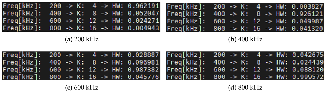
The SDFT module was physically validated on the visible optical link of the VLC platform described in Section 3.4. The link was used to transmit the four target carrier frequencies, , , , and , one at a time. The FPGA-implemented SDFT module processes the received signal and, leveraging its built-in bin selection functionality, returns the magnitude associated with the corresponding tone.
The results in Figure 7 verify that the implemented SDFT block can identify the target tones in physical FPGA operation. However, because the validation is performed with isolated tones, the results do not correspond to a full validation of simultaneous frequency-multiplexed VLP reception.
6.2. MLP Hardware Numerical Validation
The MLP inference engine was validated using the dataset described in Section 3.3. A MATLAB® reference model was used to generate golden outputs. The FPGA outputs were compared against this reference to quantify numerical fidelity. Therefore, the reported MSE values in Table 4 are hardware/software agreement metrics; they do not represent a new end-to-end physical positioning measurement.
The offline spatial-positioning baseline shown in Figure 8 indicates that approximately 90% of the estimated positions exhibit an error below 1.73 mm, corresponding to a spatial accuracy range of approximately 1–2 mm for the reference VLP dataset/model. In contrast, the MLP MSE values reported in Table 4 quantify the FPGA HW/SW numerical fidelity with respect to the offline software reference.
6.3. Resource Utilization
Table 2 summarizes the percentage resource utilization of each individually implemented module on the XA Zynq-7000 device. The SDFT block consumes 16.28% of LUTs, 17.14% of BRAM, and 21.82% of DSPs. Among the MLP variants, the sequential accumulator has the lowest resource usage, while the floating-point tree-reduction and BLAS-based designs require substantially more LUTs and DSPs. The fixed-point tree-reduction implementation reduces LUT and DSP consumption relative to the floating-point tree-reduction design, although it increases BRAM usage.
Table 3 reports a derived block-level resource estimate for a sequential receiver using one SDFT module combined with one MLP variant. The estimate is obtained by summing the individual synthesized module utilizations reported in Table 2. The values do not correspond to a complete post-implementation receiver and exclude additional control logic, interconnect, ADC interfaces, buffering, and PS/PL communication. However, they provide a useful first-order assessment of implementation feasibility on the target FPGA. In particular, the table enables a direct evaluation of the resource headroom available for each SDFT–MLP configuration and helps identify which variants are more suitable for deployment under the resource constraints of a selected device.
6.4. Latency and Numerical Fidelity
To measure processing latency, both the SDFT and MLP modules feature an output signal indicating the end of an operation. A custom VHDL-based module counts the clock cycles between two consecutive rising edges of this signal, providing the exact execution time per result. With both modules configured in free-running mode at a validation clock frequency of (), Table 4 reports both the measured clock-cycle counts and corrected time conversions.
The SDFT block has the largest latency, requiring 61658 cycles, equivalent to 616580 ns or 616.58 μs. The MLP latency depends on the architecture. The sequential accumulator requires 66.12 μs, while the BLAS-based implementation requires 6.06 μs. Therefore, the BLAS-based implementation provides an approximately 11× latency reduction relative to the sequential accumulator. All MLP variants maintain HW/SW MSE values on the order of with respect to the offline software reference, indicating that the FPGA implementations preserve the numerical behavior of the trained model.
6.5. Sequential and Projected Parallel Scalability
Table 5 summarizes the latency and update-rate estimates derived from the measured module latencies. In the sequential configuration, a single SDFT module is time-multiplexed and reused to process the four receiver channels, after which the resulting feature vector is processed by one selected MLP variant. Consequently, the total SDFT contribution is estimated as four times , plus the latency of the corresponding MLP implementation. In contrast, the parallel configuration employs four independent SDFT instances, allowing the four receiver channels to be processed concurrently; therefore, the SDFT contribution is limited to a single processing interval, followed by the selected MLP latency. These values are block-level estimates and do not include unmeasured ADC acquisition overhead, buffering, PS/PL communication, or continuous I/O scheduling.
The sequential architecture is the feasible option for the low-cost Zynq-7000 device. The projected parallel configuration reduces latency by instantiating four SDFT blocks, allowing the four receiver channels to be processed concurrently; however, this option targets larger FPGA devices and was not physically implemented on the Zynq-7000 platform in this study. The metric Approx. updates/s represents an approximate upper bound on the number of position estimates that could be produced per second, calculated from the corresponding block-level latency. For the sequential configuration, the selected MLP variant has only a minor effect on this metric, since the latency is dominated by the four consecutive SDFT processing intervals. In contrast, for the parallel configuration, the MLP latency becomes more relevant, producing differences on the order of position updates per second among the evaluated variants.
6.6. Considerations for a Real-Time VLP Receiver
The present validation focuses on the physical FPGA implementation and modular evaluation of the SDFT and MLP processing blocks. A future end-to-end digital VLP receiver would require integrating these modules into a continuous FPGA-based processing chain capable of transforming synchronized multi-channel ADC samples into position estimates. Since the optical link and analog front-end are assumed to be previously validated, the remaining integration challenges are mainly associated with the digital receiver architecture. This includes deterministic sampling, channel-aligned buffering, data scheduling, feature-vector assembly, memory organization, and control logic. In a sequential implementation, a single SDFT core would be time-multiplexed across the four receiver channels before constructing the 16-component input vector required by the MLP. In contrast, a parallel implementation would instantiate four SDFT cores to process the receiver channels concurrently, reducing latency at the expense of higher FPGA resource utilization.
The complete digital integration must also preserve consistency with the offline reference processing chain. This requires selecting the target frequency bins, computing the corresponding magnitudes, applying equivalent scaling and numerical representations, and delivering the resulting features to the MLP inference engine under sustained real-time operation. The weights, biases, activation-function lookup tables, intermediate buffers, and output registers must be coordinated by dedicated control logic while minimizing unnecessary PS/PL communication in the critical processing path. Future integration will focus on extending the validated SDFT and MLP modules into a continuous FPGA-based digital receiver, including ADC interfaces, buffering, interconnect, memory access, and control logic. This complete implementation will allow the characterization of system-level timing, maximum operating frequency, power consumption, sustained throughput, and continuous coordinate-output generation.
7. Conclusion
This work presented a hardware-oriented FPGA feasibility study of two core processing blocks required for future real-time VLP receivers: an SDFT-based spectral pre-processing module and an MLP-based inference engine. The study was deliberately framed as a modular hardware validation, not as a complete end-to-end VLP implementation.
The SDFT and MLP blocks were physically implemented and evaluated on a Xilinx® XA Zynq-7000 (xa7z020clg484-1Q) device operating at . The SDFT block required 61658 cycles, corresponding to . The MLP implementations required between and depending on the selected architecture. The BLAS-based MLP achieved the lowest latency, whereas the sequential accumulator achieved the lowest resource usage. All MLP variants reproduced the offline software reference with HW/SW MSE values on the order of .
The fixed-point tree-reduction implementation using ap_fixed〈24,10〉 provided a favorable resource/numerical-fidelity trade-off, reducing LUT and DSP usage relative to the floating-point tree-reduction design while preserving numerical fidelity. The analysis also showed that a sequential SDFT+MLP architecture is the practical option for the low-cost Zynq-7000 device, whereas a parallel four-SDFT architecture should be considered a projected scalability option for larger FPGAs.
The positioning accuracy reported in this study corresponds to the offline VLP reference dataset and model, not to a complete real-time FPGA-based VLP measurement. The FPGA results demonstrate hardware feasibility and numerical fidelity of the processing blocks. The next steps toward a complete system are simultaneous multi-tone SDFT validation, integration of the PD/ADC acquisition chain, continuous buffering and I/O scheduling, power measurement, maximum-frequency characterization, sustained throughput evaluation, and final end-to-end VLP validation.
Author Contributions
Conceptualization, Randy Lozada Domínguez and Jianming Tang; Methodology, Randy Lozada Domínguez and Enrique San Millán Heredia; Software, Randy Lozada Domínguez and Aran White; Validation, Randy Lozada Domínguez; Formal analysis, Randy Lozada Domínguez; Investigation, Randy Lozada Domínguez and Aran White; Resources, Randy Lozada Domínguez; Data curation, Randy Lozada Domínguez and Aran White; Writing – original draft, Randy Lozada Domínguez; Writing – review & editing, Randy Lozada Domínguez, Jianming Tang and Enrique San Millán Heredia; Supervision, Jianming Tang; Project administration, Jianming Tang. All authors have read and agreed to the published version of the manuscript.
Funding
This research was funded by Spanish State Research Agency grant number DIN2021-012133.
Data Availability Statement
The original contributions presented in this study are included in the article. Further inquiries can be directed to the corresponding author.
Conflicts of Interest
The authors declare no conflicts of interest.
References
- Hu, J.; Gong, C.; Xu, Z. Demonstration of A Robot Controlling and Positioning System Based on Visible Light. 2017 IEEE Globecom Workshops (GC Wkshps), 2017; pp. 1–6. [Google Scholar] [CrossRef]
- Kim, H.S.; Kwon, D.H.; Yang, S.H.; Son, Y.H.; Han, S.K. Implementation of Real-Time Indoor Positioning System Using Carrier Allocation Visible Light Communication. The 12th International Conference on Optical Internet Proceedings (ICOIN), 2013; pp. TP–43. [Google Scholar]
- Liu, H.; Darabi, H.; Banerjee, P.; Liu, J. Survey of Wireless Indoor Positioning Techniques and Systems. IEEE Trans. Syst. Man. Cybern. Part C (Applications and Reviews) 2007, 37, 1067–1080. [Google Scholar] [CrossRef]
- Ghassemlooy, Z.; Alves, L.N.; Zvanovec, S. Visible Light Communications: Theory and Applications; CRC Press, 2017. [Google Scholar]
- Li, H.; Huang, H.; Xu, Y.; Wei, Z.; Yuan, S.; Lin, P.; Wu, H.; Lei, W.; Fang, J.; Chen, Z. A Fast and High-Accuracy Real-Time Visible Light Positioning System Based on Single LED Lamp With a Beacon. IEEE Photonics J. 2020, 12, 1–15. [Google Scholar] [CrossRef]
- Yu, B.; Liu, X.; Chen, Y.; Guo, L.; Bao, J. Image Processing Based on Inter-frame Color Feature Matching for Visible Light Positioning. 2024 2nd International Conference on Signal Processing and Intelligent Computing (SPIC), 2024; pp. 1–6. [Google Scholar] [CrossRef]
- Apolo, J.A.; Osahon, I.N.O.; Ortega, B.; Almenar, V.; Tang, J.; Rajbhandari, S. Experimental demonstrations of high-accuracy 3D/2D indoor visible light positioning using imaging multiple-input multiple-output receivers and artificial neural networks. IET Optoelectron. 2025. [Google Scholar] [CrossRef]
- Chen, Y.; Guan, W.; Li, J.; Song, H. Indoor Real-Time 3-D Visible Light Positioning System Using Fingerprinting and Extreme Learning Machine. IEEE Access 2020, 8, 13875–13886. [Google Scholar] [CrossRef]
- Randy, L.D.; Sebastián, B.P.J.; Enrique, S.M.H. Time Synchronization Technique Hardware Implementation for OFDM Systems With Hermitian Symmetry for VLC Applications. IEEE Access 2023, 11, 42222–42233. [Google Scholar] [CrossRef]
- Perlaza, J.S.B.; Domínguez, R.L.; Heredia, E.S.M. Phase Characterization and Correction in a Hardware Implementation of an OFDM-Based System for VLC Applications. IEEE Photonics Journal 2023, 15, 1–7. [Google Scholar] [CrossRef]
- Trenz Electronic GmbH. TE0720 Resources. 2024. Available online: https://wiki.trenz-electronic.de/display/PD/TE0720+Resources (accessed on 2025-10-05).
- Jacobsen, E.; Lyons, R.G. The Sliding DFT. IEEE Signal Process. Mag. 2003, 20, 74–80. [Google Scholar] [CrossRef]
- Xilinx Inc. Fast Fourier Transform v9.1 Logicore. Xilinx 2019, PG109, 1–97. [Google Scholar]
- Córdoba, F.J.; Requena, A. Fast Approximations to the Magnitude of a Complex Number. Electron. Lett. 1993, 29, 209–210. [Google Scholar] [CrossRef]
- Alam, S.M.K.; Ruehli, A.E. Approximation Algorithms for the Magnitude of a Complex Number. Electron. Lett. 1990, 26, 324–326. [Google Scholar] [CrossRef]
- Blelloch, G.E. Prefix sums and their applications; Technical Report CMU-CS-90-190; Carnegie Mellon University, 1990. [Google Scholar]
- Chen, Y.H.; Emer, J.; Sze, V. Diannao: A small-footprint high-throughput accelerator for ubiquitous machine-learning. ACM SIGARCH Comput. Archit. News 2014, 42, 269–284. [Google Scholar]
- Zhang, C.; Li, P.; Sun, G.; Guan, Y.; Xiao, B.; Cong, J. Optimizing FPGA-based accelerator design for deep convolutional neural networks. In Proceedings of the Proceedings of the 2015 ACM/SIGDA International Symposium on Field-Programmable Gate Arrays, 2015; ACM; pp. 161–170. [Google Scholar]
- Gupta, S.; Agrawal, A.; Gopalakrishnan, K.; Narayanan, P. Deep learning with limited numerical precision. In Proceedings of the International Conference on Machine Learning, 2015; pp. 1737–1746. [Google Scholar]
- Xilinx, Inc. Xilinx BLAS Library User Guide. 2023. Available online: https://www.xilinx.com/support/documentation/user_guides/ug1409-vivado-bsp-blas.pdf.
- Vogl, T.P.; Mangis, J.K.; Rigler, A.K.; Zink, W.T.; Alkon, D.L. Accelerating the convergence of the back-propagation method. Biol. Cybern. 1988, 59, 257–263. [Google Scholar] [CrossRef]
Figure 1.
Reference Multi-PD VLP system and laboratory setup used to generate the offline dataset. The FPGA receiver is proposed as a future replacement for the offline processing chain, but the complete end-to-end VLP system is not experimentally integrated in this work.
Figure 1.
Reference Multi-PD VLP system and laboratory setup used to generate the offline dataset. The FPGA receiver is proposed as a future replacement for the offline processing chain, but the complete end-to-end VLP system is not experimentally integrated in this work.
| [ Schematic diagram of the Multi-PD VLP system considered as reference for the proposed FPGA-based receiver architecture.] [b]0.52 | [ Laboratory setup [7].] [b]0.40 |
Figure 2.
VLC platform used for physical FPGA validation of the implemented SDFT and MLP modules [9,10]. This platform is used for modular hardware validation and does not constitute a complete VLP end-to-end testbed.
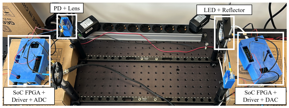
Figure 3.
Conceptual multi-channel FPGA-oriented receiver architecture. The figure illustrates the target integration path for a future receiver. In this work, only the SDFT + SDFT Bin Selection and MLP blocks are physically validated.
Figure 3.
Conceptual multi-channel FPGA-oriented receiver architecture. The figure illustrates the target integration path for a future receiver. In this work, only the SDFT + SDFT Bin Selection and MLP blocks are physically validated.
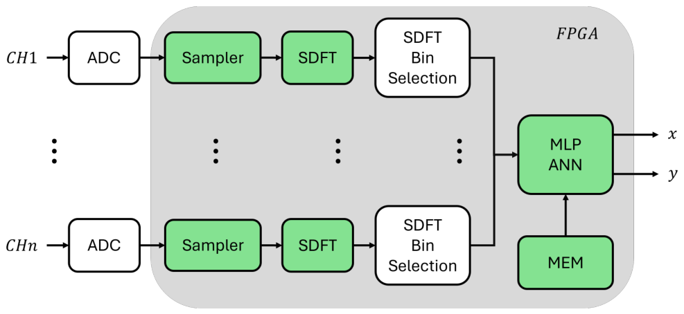
Figure 4.
Authors’ FPGA-oriented development workflow. The proposed methodology describes the complete path from software reference modeling and golden-data generation to hardware-oriented design, HLS-based RTL generation, FPGA/SoC integration, embedded-software control, physical deployment, and hardware validation. In this work, the flow is applied to the SDFT and MLP hardware modules.
Figure 4.
Authors’ FPGA-oriented development workflow. The proposed methodology describes the complete path from software reference modeling and golden-data generation to hardware-oriented design, HLS-based RTL generation, FPGA/SoC integration, embedded-software control, physical deployment, and hardware validation. In this work, the flow is applied to the SDFT and MLP hardware modules.
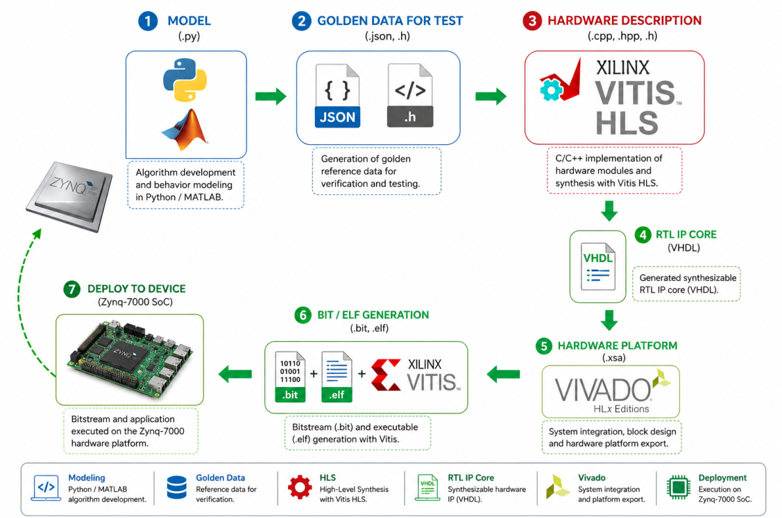
Figure 5.
SDFT proposed architecture.
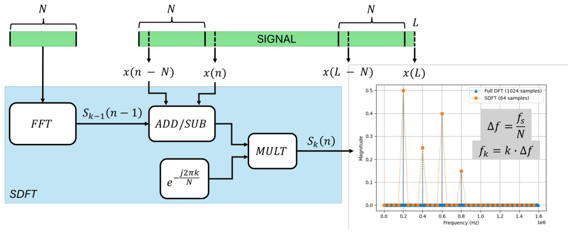
Figure 6.
Comparison of sequential accumulation (left) and tree reduction (right) for summing four elements.
Figure 6.
Comparison of sequential accumulation (left) and tree reduction (right) for summing four elements.
| [Sequential Accumulation] [b]0.48 | [Tree Reduction] [b]0.48 |
Figure 7.
Physical FPGA output—-displayed on the UART terminal console during real-time execution of the SDFT module–for individual input carrier frequencies transmitted through the visible optical link: (a) 200 kHz, (b) 400 kHz, (c) 600 kHz, and (d) 800 kHz. The validation is performed one tone at a time and does not demonstrate simultaneous multi-tone VLP operation.
Figure 7.
Physical FPGA output—-displayed on the UART terminal console during real-time execution of the SDFT module–for individual input carrier frequencies transmitted through the visible optical link: (a) 200 kHz, (b) 400 kHz, (c) 600 kHz, and (d) 800 kHz. The validation is performed one tone at a time and does not demonstrate simultaneous multi-tone VLP operation.
| [200 kHz] [b]0.48 | [400 kHz] [b]0.48 |
| [600 kHz] [b]0.48 | [800 kHz] [b]0.48 |
Figure 8.
Offline spatial-positioning baseline obtained from the experimental VLP dataset and software reference model. These results should not be interpreted as end-to-end real-time positioning accuracy measured directly from the FPGA receiver.
Figure 8.
Offline spatial-positioning baseline obtained from the experimental VLP dataset and software reference model. These results should not be interpreted as end-to-end real-time positioning accuracy measured directly from the FPGA receiver.
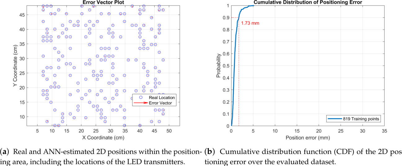
| [ Real and ANN-estimated 2D positions within the positioning area, including the locations of the LED transmitters.] [b]0.48 | [ Cumulative distribution function (CDF) of the 2D positioning error over the evaluated dataset.] [b]0.48 |

Table 1.
Synthesized comparison of representative VLP receivers and the proposed FPGA-oriented modular implementation.
Table 1.
Synthesized comparison of representative VLP receivers and the proposed FPGA-oriented modular implementation.
| Work | Reception method | Reception algorithm / main modules | Metrics | Real-time | HW platform | Relation to this work |
|---|---|---|---|---|---|---|
| Kim et al. [2] | PD-based CA-VLC | RF-carrier allocation; RSS-based trilateration; FPGA-assisted acquisition and PC/MATLAB® position estimation | Error within 7 cm in a 100×100×275 cm3 space. | System-level real-time; PC-based estimation | Rx FPGA + ADC for digital acquisition; UART link to PC; MATLAB® used for Rx position estimation | Demonstrates carrier-allocation VLC positioning with FPGA-assisted acquisition and RF-carrier separation, but the final position estimation is performed on a PC using MATLAB. In contrast, our work focuses on migrating the main receiver processing blocks, namely spectral extraction and neural-network inference, to physical FPGA hardware. |
| Hu et al. [1] | PD-based receiver | Low-complexity RSS-difference positioning with TD LED groups; OOK downlink, adaptive thresholding, synchronization, demodulation and MAC. | Average positioning error around 10 cm; response time below 100 ms. | Yes | LED drivers, custom PD board with amplifier and MCU, central PC, WiFi uplink | Demonstrates low-cost real-time PD-based robot positioning; our work instead targets FPGA spectral extraction and neural inference for higher-accuracy VLP blocks. |
| Li et al. [5] | IS-based CMOS rolling-shutter receiver | Unbalanced single-LED VLP with beacon; OOK downlink; ROI detection, fast beacon search and trigonometric positioning. | Mean error 2.26 cm at 3 m; average time 6.3 ms on laptop and 60 ms on embedded platform. | Yes | CMOS OV2640, Ingenic X1500 embedded processor, laptop for configuration | Relevant as a real-time image-sensor baseline; our work avoids image processing by using PD-domain SDFT and FPGA MLP inference. |
| Chen et al. [8] | PD-based receiver | RSS fingerprinting with ELM and VLP kernel; CDMA LED identification, ADC/RSSI acquisition and software positioning. | Real-world average 3D error 0.0365 m; average time 0.00177 s. | Yes | STM32F407ZG, PD circuit, ADC/comparator, PC/Python | Closely related through ML-based VLP; our work focuses on FPGA implementation of spectral pre-processing and MLP inference. |
| Yu et al. [6] | IS-based image receiver | Inter-frame color feature matching; equidistant sampling, low-complexity decoding, LED-ROI tracking. | Average positioning delay 80.2 ms; landmark decoding rate reported as 100% under normal communication distance. | Yes, delay-oriented | Not explicitly reported | Shows latency reduction for IS-based VLP; our work targets a different PD/FPGA path where image processing is not required. |
| Apolo et al. [7] | Imaging MIMO receiver with 4 PDs and lens | FDM/FFT RSS extraction from four LEDs followed by supervised MLP-ANN for 2D/3D positioning. | Experimental 2D/3D errors: 3.7/51 mm; simulation: 2/14.7 mm. | No; offline processing | AWGs, 4 LEDs, 4-PD imaging receiver, oscilloscope, MATLAB®/ZEMAX | Direct experimental reference for the dataset and algorithmic chain; our work studies FPGA migration of the SDFT/MLP processing blocks. |
| This work | FPGA-oriented PD-based VLP receiver blocks | SDFT magnitude extraction plus hardware-optimized MLP; sequential, tree-reduction, fixed-point and BLAS MLP variants. | SDFT: 616.58 s; MLP: 6.06–66.12 s; sequential receiver estimate: 2.49–2.73 ms; MLP HW/SW MSE ∼10−6. | Modular real-time HW validation; not end-to-end VLP | Xilinx XA Zynq-7000 @ 100 MHz, existing VLC validation platform | Provides physical FPGA validation of the computational blocks needed to move high-accuracy VLP from offline processing toward embedded real-time implementation. |
Table 2.
Percentage of XA Zynq-7000 (xa7z020clg484-1Q) [11] resource utilization for each physically implemented module.
Table 2.
Percentage of XA Zynq-7000 (xa7z020clg484-1Q) [11] resource utilization for each physically implemented module.
| Module | LUT | LUTRAM | FF | BRAM | DSP |
|---|---|---|---|---|---|
| SDFT | 16.28 | 4.38 | 6.20 | 17.14 | 21.82 |
| MLP (Seq. Acc.) | 9.71 | 0.39 | 3.11 | 4.64 | 4.55 |
| MLP (FTR) | 45.23 | 6.31 | 16.30 | 35.36 | 34.55 |
| MLP (APTR) | 23.64 | 4.40 | 6.83 | 46.79 | 10.91 |
| MLP (BLAS) | 47.07 | 2.51 | 17.06 | 13.93 | 48.18 |
Table 3.
First-order block-level resource estimate for a sequential SDFT+MLP configuration. Values are arithmetic sums of the individual module reports and exclude complete-system overhead.
Table 3.
First-order block-level resource estimate for a sequential SDFT+MLP configuration. Values are arithmetic sums of the individual module reports and exclude complete-system overhead.
| Configuration | LUT | LUTRAM | FF | BRAM | DSP |
|---|---|---|---|---|---|
| SDFT+MLP(Seq.) | 25.99 | 4.77 | 9.31 | 21.78 | 26.37 |
| SDFT+MLP(FTR) | 61.51 | 10.69 | 22.50 | 52.50 | 56.37 |
| SDFT+MLP(APTR) | 39.92 | 8.78 | 13.03 | 63.93 | 32.73 |
| SDFT+MLP(BLAS) | 63.35 | 6.89 | 23.26 | 31.07 | 70.00 |
Table 4.
Module-level latency and HW/SW MSE of the physically implemented FPGA blocks @ on the XA Zynq-7000 (xa7z020clg484-1Q) [11].
Table 4.
Module-level latency and HW/SW MSE of the physically implemented FPGA blocks @ on the XA Zynq-7000 (xa7z020clg484-1Q) [11].
| Module | Cycles | ns | s | MSE X | MSE Y |
|---|---|---|---|---|---|
| SDFT | 61658 | 616580 | 616.58 | – | – |
| MLP (Seq. Acc.) | 6612 | 66120 | 66.12 | ||
| MLP (FTR) | 2377 | 23770 | 23.77 | ||
| MLP (APTR) | 2196 | 21960 | 21.96 | ||
| MLP (BLAS) | 606 | 6060 | 6.06 |
Table 5.
Derived latency and update-rate estimates based on measured module latencies. These are block-level estimates and not complete end-to-end VLP system measurements.
Table 5.
Derived latency and update-rate estimates based on measured module latencies. These are block-level estimates and not complete end-to-end VLP system measurements.
| Configuration | MLP variant | Latency (ms) | Approx. updates/s |
|---|---|---|---|
| Sequential | Seq. Acc. | 2.532 | 394.9 |
| FTR | 2.490 | 401.6 | |
| APTR | 2.488 | 401.9 | |
| BLAS | 2.472 | 404.5 | |
| Parallel | Seq. Acc. | 0.683 | 1464.8 |
| FTR | 0.640 | 1561.6 | |
| APTR | 0.639 | 1566.1 | |
| BLAS | 0.623 | 1606.1 |
Disclaimer/Publisher’s Note: The statements, opinions and data contained in all publications are solely those of the individual author(s) and contributor(s) and not of MDPI and/or the editor(s). MDPI and/or the editor(s) disclaim responsibility for any injury to people or property resulting from any ideas, methods, instructions or products referred to in the content. |
© 2026 by the authors. Licensee MDPI, Basel, Switzerland. This article is an open access article distributed under the terms and conditions of the Creative Commons Attribution (CC BY) license.
Copyright: This open access article is published under a Creative Commons CC BY 4.0 license, which permit the free download, distribution, and reuse, provided that the author and preprint are cited in any reuse.