

Submitted:
21 July 2026
Posted:
21 July 2026
You are already at the latest version
Abstract
Taking a typical high-power microwave power supply system as the research object, this paper quantitatively simulates and compares electromagnetic disturbance characteristics under multiple operating conditions, systematically investigates the influence mechanism of the system on EMI, and verifies the proposed simulation model via prototype experiments. Firstly, the typical equipment composition and three operating modes of the system are elaborated. Standardized high-frequency equivalent circuits of thyristors, capacitors, and inductors are established, and parasitic parameters are extracted to construct a system-level high-frequency coupling model. Secondly, based on the dynamic device characteristics under resonant charging, energy recovery and energy supplement modes, the generation mechanisms of EMI are clarified with quantitative data. During modeling, the electrical characteristics of thyristor body diodes and inter-electrode capacitances are fully incorporated with reference to actual component parameters. The EMC co-simulation based on CST field-circuit coupling is adopted to collaboratively optimize all parameters, which reduces the approximation error introduced by local modeling and greatly improves simulation accuracy. Combined with simulation and prototype experimental verification, this paper reveals the multi-path EMI coupling mechanism of pulsed power systems. The proposed parasitic parameter-based SPICE modeling and field-circuit co-simulation method can provide quantitative analysis tools and theoretical support for EMC suppression design of high-power microwave power supplies.
Keywords:
high-power microwave
; electromagnetic interference
; system high-frequency model
; interference path
; interference suppression
; field-circuit co-simulation
1. Introduction
High-power pulsed drive (HPPD) sources have been widely applied in industry, military and scientific research, with continuously growing demands on output capacity, miniaturization and controllability. Pulse Forming Network-Marx (PFN-Marx) based HPPD sources stand out due to their advantages including high power output, adjustable pulse waveform, modular design and high energy conversion efficiency, which have attracted extensive research attention [1,2,3,4,5]. However, drastic voltage and current variations during energy compression and conversion will trigger severe electromagnetic interference (EMI). Meanwhile, the miniaturization trend further raises challenges for electromagnetic compatibility (EMC) design. For instance, breakdown of internal capacitors may generate fast transient overvoltages, which interfere secondary equipment through cable conductive coupling and ground potential fluctuation, and disturb surrounding cables and electronic devices via radiation. Such severe EMI may cause malfunction or permanent damage to external equipment, and even disrupt the normal operation of HPPD sources themselves. Therefore, in-depth research on EMI characteristics, coupling paths and equipment influence induced by transient overvoltages of PFN-Marx HPPD sources carries important theoretical and engineering significance [6,7,8,9,10]. Additionally, densely arranged power electronic devices inside high-power microwave power systems present remarkable mutual EMI effects. To reveal the device-level EMI interaction mechanism, high-frequency models that accurately reflect multi-device coupling effects need to be established to analyze the mechanisms of the system to EMI under various operating conditions.
Existing studies mainly focus on the radiated interference characteristics of PFN-Marx generators. Siew et al. measured the radiated field waveforms of pin-plate gas switches [11]; Fan et al. analyzed the current and radiated electric field spectra of triggered spark gaps via circuit simulation [12]; Rao et al. evaluated the EMI characteristics of HPPD sources under specific working conditions and their implications for EMC standards [13]; Yi et al. analyzed the propagation law of electromagnetic pulses (EMP) in high-power laser devices through modeling and experiments [14]; Larsson et al. investigated the propagation links of intentional EMI systems for high-power microwaves [15]; Cadilhon et al. proposed a novel strong-field measurement method based on diffractive targets [16,17]. Although the above works promote the understanding of HPPD system EMI from experimental, simulation and measurement perspectives, research gaps still exist in multi-physics coupling interference source modeling as well as the coordinated interference mechanisms of conductive and radiative paths. To fill these gaps, this paper quantitatively calculates characteristic parameters such as EMI amplitude and radiation field strength under three typical operating conditions, compares the differentiated effects of operating modes on EMI generation and propagation, and validates the model with test data.
This paper carries out the following research based on a typical high-power microwave power supply system: identifying and analyzing the main EMI sources and their propagation paths within the system. Establishing standardized high-frequency device models and CST field-circuit co-simulation platform and clarifying the EMI generation and conduction mechanisms under multiple operating conditions via simulation, and verifying the simulation model with experiments. Quantitatively analyzing the radiation impact of unshielded cables on the overall electromagnetic environment and proposing effective interference suppression strategies. During modeling, precise characterization of thyristor body diodes and inter-electrode parasitic capacitances is implemented, and global EMC co-simulation is adopted to collaboratively optimize model parameters, which significantly improves model accuracy and simulation reliability. The research results provide quantifiable theoretical basis and engineering approaches for EMC design and EMI suppression of high-power microwave power supply system
2. Typical Equipment and Operating Modes of High-Power Microwave Systems
2.1. Test Typical System Components
The high-power microwave system consists of generators, inverter power supplies, charging units, energy supplement unit, cables, inductors, capacitors and other assemblies, as shown in Figure 1. The inverter converts low-voltage DC into 220 V AC to power charging units, which supply 1 kV and 1.8 kV medium-voltage DC to primary capacitor C1 and intermediate storage capacitor C2 respectively. After full charging of C1 and C2, the voltage of C1 is boosted by a transformer to feed the PFN-Marx generator. The PFN-Marx is composed of series-connected capacitors and inductors; once fully charged, energy is released via switch actions to generate pulsed voltage that drives microwave devices to produce stable electron beams. After one discharge cycle, energy recovery inductors L1 and L2 recycle the residual reverse voltage on C1 through the energy recovery circuit. Finally, C2 replenishes energy to restore C1 to its initial voltage. Generally, the capacity of C2 is far larger than C1 to support repeated cyclic operation.
2.2. System Operating Modes
The high-power microwave driver is divided into three sub-systems: primary boost unit, energy supplement unit and resonant boost unit. The primary boosting unit converts low-voltage DC to high voltage for capacitor charging and is isolated after charging; subsequent analysis focuses on the energy supplement and resonant boost unit. The energy supplement unit consists of primary capacitor C1, intermediate storage capacitor C2, thyristors S1, S2, S3 and energy recovery inductors L1, L2 for energy replenishment. The resonant boosting unit is composed of transformers and PFN-Marx, which realizes short-time voltage boosting and pulse square-wave modulation to output quasi-square high-voltage pulses with a width of hundreds of nanoseconds.
Mode 1: Resonant Charging. As shown in Figure 2, at the initial stage, C2 and C1 are charged to U2 and U1 respectively. Main thyristor S1 turns on, and C1 charges the capacitors inside PFN-Marx via the transformer. After charging completes, the gas spark gap breaks down to discharge the load. S1 turns off automatically when charging current crosses zero, leaving residual reverse voltage on C1. An equivalent impedance replaces the PFN-Marx in the topology.
Mode 2: Energy Recovery. As shown in Figure 3, thyristor S₂ conducts, and the residual reverse voltage on C1 is recycled via the energy recovery circuit.
Mode 3: Energy Supplement. As shown in Figure 4, thyristor S3 turns on, and C2 charges C1 while energy recovery thyristor S2 turns off due to zero current. S3 switches off automatically once C1 recovers to U₁ and the charging current of C2 drops to zero; the voltage of C2 decreases from U2 to U₂’. The completion of this process marks the end of one full operating cycle.
When the primary energy storage sub-system operates at a repetitive frequency, the above charging-discharging cycles repeat. Adjusting the conduction intervals of energy recovery and supplement thyristors enables C1 to recover its initial voltage after each pulse, guaranteeing stable cyclic operation, as illustrated by the switch timing diagram in Figure 5.
2.3. Quantitative Comparison of EMI Under Different Operating Modes
In order to quantitatively distinguish the EMI and propagation characteristics of the three modes, the voltage waveforms of high-power microwave systems were tested to extract transient interference voltage and oscillation duration, as shown in Table 1.
Figure 6.
(a)The input voltage waveform of PFN-Marx (b) The waveform when the thyristor is conducting.
Figure 6.
(a)The input voltage waveform of PFN-Marx (b) The waveform when the thyristor is conducting.
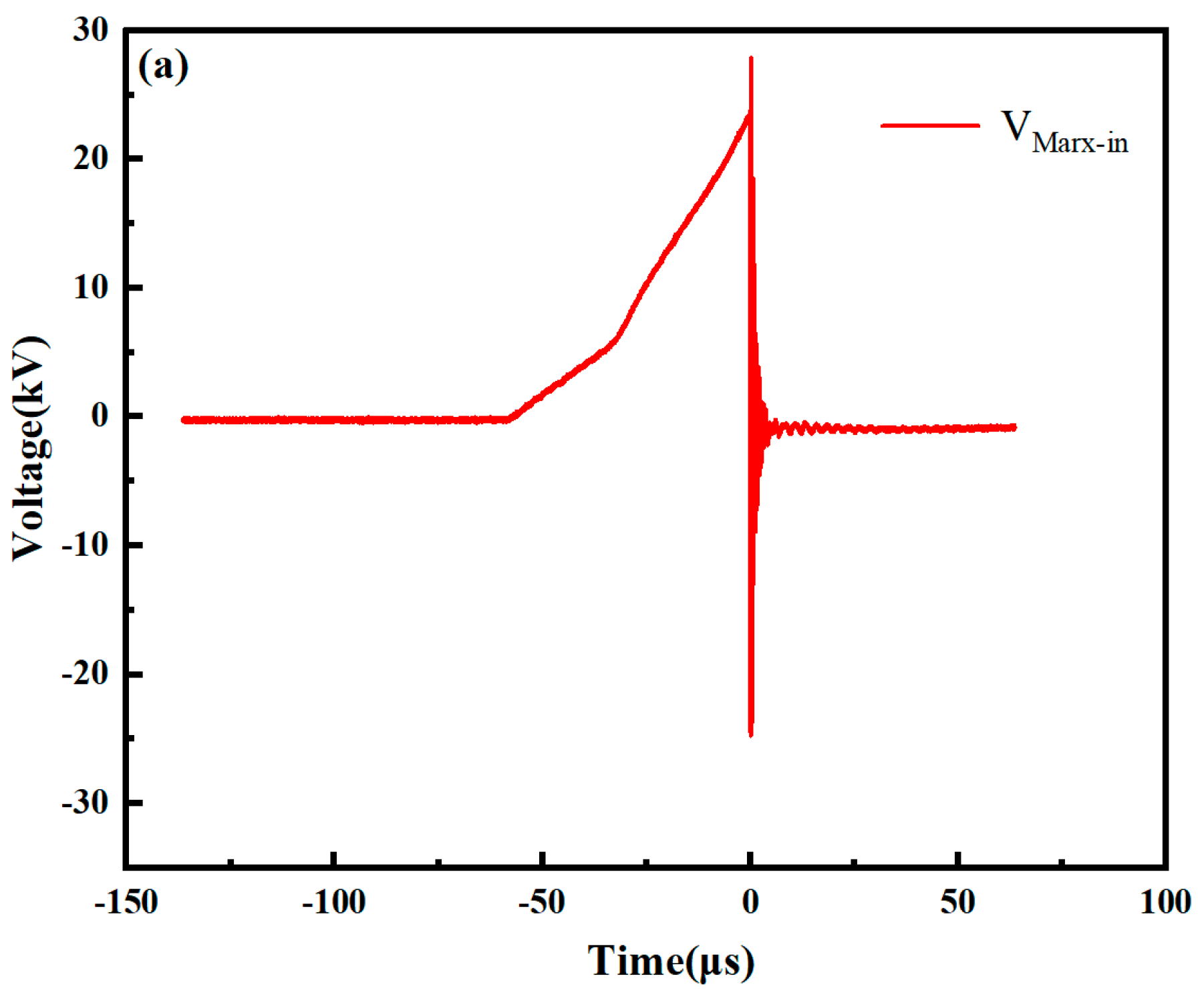
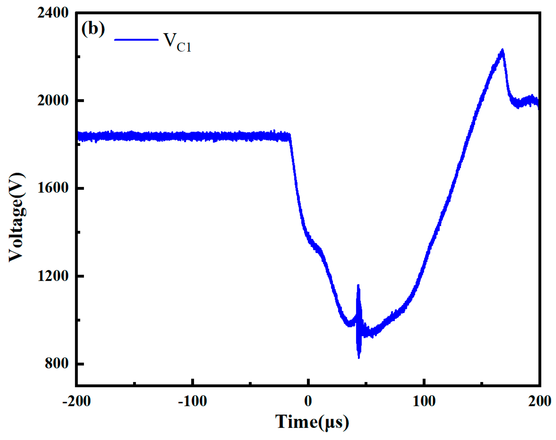
Combined with the quantitative data in Table 1, the following conclusions can be drawn: During resonant charging (Mode 1), nanosecond breakdown of the gas spark gap generates a voltage change rate up to 10¹² V/s. Coupled with fast switching of thyristor S₁, conductive and radiated interference with the largest amplitude and longest oscillation time is induced, which acts as the core disturbance source of the system. Only thyristor S₂ operates in energy recovery mode without spark gap breakdown, resulting in significantly reduced di/dt and du/dt. Nevertheless, transient interference is still introduced due to coupling from the spark gap switch.
3. EMI Generation Mechanism of Primary Energy Storage Subsystem
The main EMI sources inside the high-power microwave system include gas spark switch, transformer and thyristors of the PFN-Marx, among which the gas spark gap produces the strongest interference. Therefore, analyzing the EMI characteristics of PFN-Marx carries great significance. This section briefly introduces the composition and operating principle of PFN-Marx, and focuses on analyzing the EMI generation mechanism of primary and secondary circuits.
3.1. Operating Principle of PFN-Marx
The PFN-Marx pulse generator integrates the core advantages of pulse forming networks and Marx generators, featuring high-efficiency voltage multiplication and precise pulse shaping capability. Compared with traditional Marx generators that produce double-exponential triangular pulses, PFN-Marx delivers pulses with flatter tops and wider effective pulse widths, greatly improving energy transmission efficiency and load matching performance. Figure 7 shows the circuit topology of the inductor-isolated PFN-Marx adopted in this research. Its operating principle relies on sequential switching between parallel charging and series discharging of capacitors: high-voltage DC power supplies charge multi-stage energy storage capacitors of the LC ladder network in parallel, with gas spark gaps providing electrical isolation between stages. Trigger signals sequentially break down each switch to instantly switch capacitors from parallel to series connection, realizing voltage superposition and high-voltage pulse output. Equal capacitance C and equal inductance L are adopted for all stages, i.e., Lᵢ=L, Cᵢ=C (i=1,2,3…).
3.2. Equivalent Model of PFN-Marx
The operation of PFN-Marx is divided into three typical stages: parallel charging, triggering and cascaded conduction, series discharging and pulse forming, each involving complex electromagnetic transients that directly affect output pulse quality and system EMC performance.
Parallel Charging Stage: All gas spark gaps remain open with high impedance. Each PFN energy storage module is connected to C2 via isolation inductors. After voltage transformation (42 kV) by the transformer, C2 slowly charges all parallel PFN capacitors, which eventually reach an identical voltage V0 under ideal conditions.
Triggering and Cascaded Conduction Stage: External trigger signal acts on the first-stage spark gap for initial breakdown, which sharply drops its terminal voltage and lifts the upper potential of the second-stage capacitor to nearly 2V₀, exceeding the static breakdown voltage of the second spark gap to trigger rapid conduction. Subsequent gaps break down in sequence to form a cascaded avalanche effect. The voltage change rate at breakdown reaches 10¹² V/s, generating high-frequency conductive interference via displacement current through switch parasitic capacitances, and strong radiated interference excited by fast-rising current edges.
Series Discharging and Pulse Forming Stage: All switches turn on, switching N PFN modules from parallel to series connection, with theoretical output voltage N·V₀.
Figure 8.
PFN Marx equivalent circuit topology diagram.
3.3. EMI Generation Mechanism of PFN-Marx
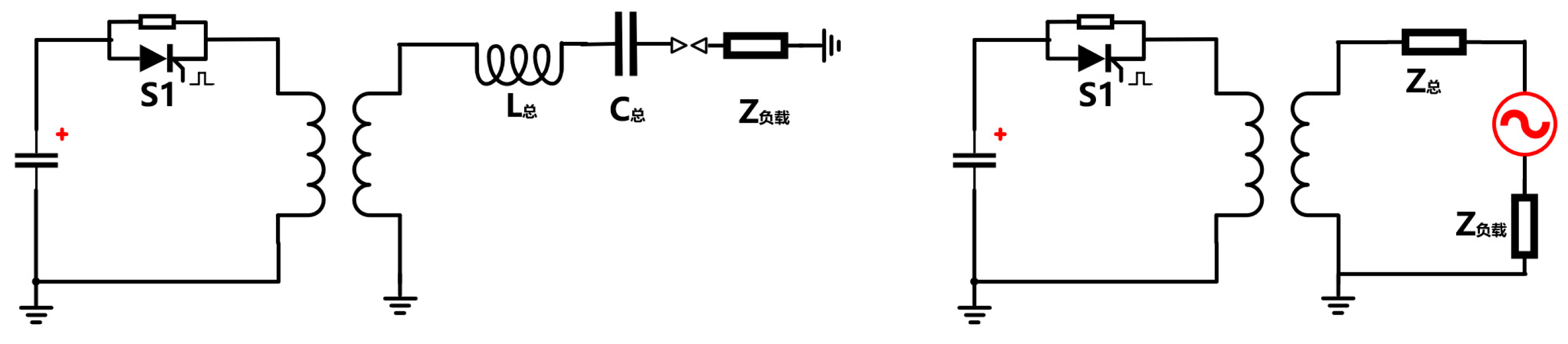
By combining pulse forming networks and Marx generators, PFN-Marx releases stored energy within nanoseconds to generate high-amplitude, fast-front high-voltage pulses. Rapid current rise within nanoseconds induces intense magnetic field variations to produce radiated interference. When multi-stage capacitors discharge in series, voltage jumps to hundreds of kilovolts in an instant, propagating through power lines and ground wires to form conductive interference that disturbs connected electronic equipment. Fast switching of power devices generates waveforms with high du/dt and di/dt, which act as system disturbance sources. After thyristor S₁ turns on, induced electromotive force e_L is generated on the primary transformer winding, and mutual electromotive force e_M is induced on the secondary winding to charge the capacitors of PFN-Marx, whose equivalent circuit is shown in the red dashed box of Figure 9.
4. High-Frequency EMI Modeling of Typical Equipment and the Whole System
As demonstrated in the previous section, transient electromagnetic disturbance generated by the resonant voltage division unit of the primary energy storage sub-system propagates via conduction and radiation to interfere with the high-power microwave driver. To deeply analyze conductive EMI induced by gas spark gaps, a field-circuit co-simulation modeling method is adopted in this paper: Establish equivalent circuit models for each component based on their electromagnetic characteristics; Calculate parasitic parameters of key components via electromagnetic field numerical simulation to provide accurate inputs for equivalent circuits; Integrate all sub-module models to build a complete circuit model of system-level conductive interference coupling paths.
4.1. Operating Principle of PFN-Marx
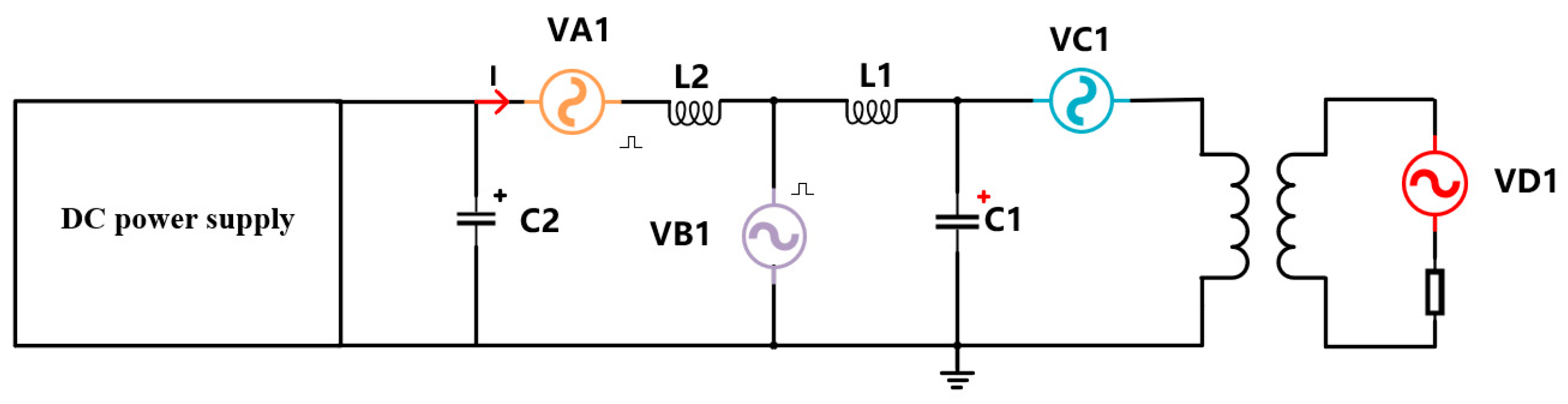
High-frequency EMI models are established for all typical components of the high-power microwave system shown in Figure 1. The primary voltage boosting unit is connected to the driver via DC cables, and the driver system contains capacitors, recovery inductors, busbars, thyristor modules, transformers and PFN-Marx, with its output terminal connected to microwave loads. Each component is represented by its high-frequency model to construct conductive path models. Based on the substitution theorem, thyristor branches are replaced by voltage sources VA1, VB1, VC1, VD1 whose waveforms match the anode-cathode voltage of the substituted thyristors.
Figure 10.
Equivalent Interference Topology of High Power Microwave System Circuit.
4.2. High-Frequency Models of Key Components
Figure 11 presents the impedance curves and corresponding high-frequency equivalent circuits of C1, C2, L1 and L1 measured by an impedance analyzer. Energy recovery inductors L1 and L2 adopt multiple equivalent models for different simulation scenarios: Simplified RL model for low-frequency steady-state charging-discharging calculation; Second-order RLC resonant model for conductive interference time-domain simulation (incorporating winding parasitic capacitance); High-order model with additional lead stray parameters for 10 MHz high-frequency full-wave radiation simulation, balancing calculation accuracy and efficiency.
4.3. High-Frequency Models of Key Components
The thyristor adopted in this work is CRRC MKP9 030-042, with key parameters extracted from its datasheet: peak pulse current 30 kA, repetitive off-state voltage 4200 V, repetitive reverse voltage 4200 V, critical on-state current rise rate 3000 A/μs, critical on-state voltage rise rate 2000 V/μs, rated average forward current 30 A, gate trigger current 300 mA, maximum steady-state operating current 30 A. This subsection introduces the parameter extraction method to build functional and EMC-compliant SPICE models.
After simplification and approximation, the SPICE I-V characteristic equations are written as Eq. (1):
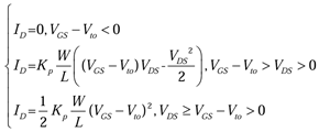
Parameter Explanation for Eq. (1). ID: Equivalent channel current of thyristor, A; KP: Device transconductance coefficient; W/L: Equivalent channel width-to-length ratio; VGS: Gate-cathode driving voltage, V; VTO: Thyristor turn-on threshold voltage, V; VDS: Anode-cathode terminal voltage, V.
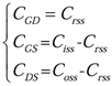
Thyristor parasitic capacitances dominate the device’s EMC performance, which affect switching dv/dt, di/dt and EMI propagation. C-V curves measured by impedance analyzer are shown in Figure 12. Input capacitance Ciss, output capacitance Coss.
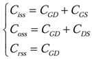
Feedback capacitance Crss are converted to gate-drain CGD, gate-source CGS and drain-source CDS.
5. Field-Circuit Co-Simulation Analysis
Thyristor and transformer SPICE models are imported into the Circuits module, together with equivalent circuits of L₁, L₂, C1, C2. DC 15 V control voltage is applied to thyristor gates, a 0.1 Ω resistor simulates grounding resistance, and a 50 Ω resistor acts as output load. A 1.8 kV measured voltage excitation is injected at the positive terminal of C₁ (probe P2), and the complete system simulation circuit is shown in Figure 13.
5.1. High-Frequency Models of Key Components
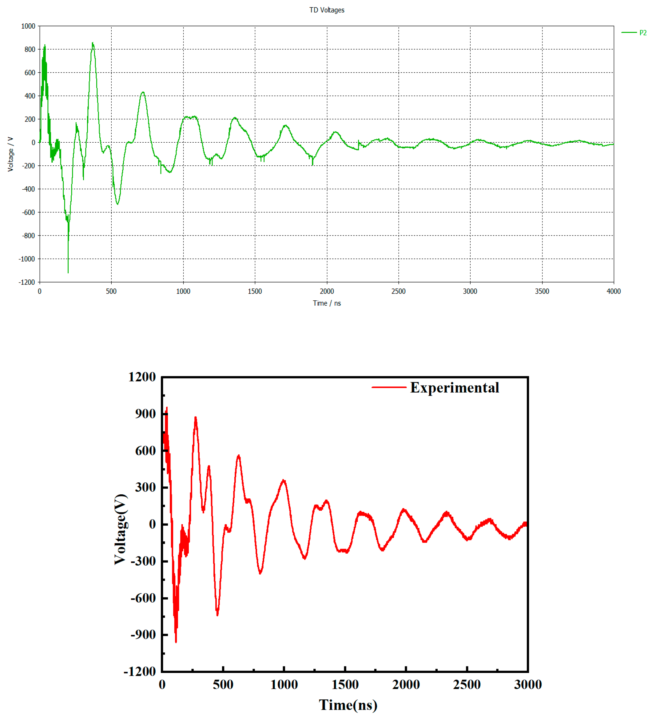
Figure 15 compares simulated and experimental voltage waveforms at probe P2 (positive terminal of C₁). The simulated waveform features a positive peak of 926 V and negative peak of -1180 V with high-frequency oscillation lasting 3200 ns. Severe front-end oscillation originates from coupled di/dt of fast-switched S₁ and parasitic LC resonance of multi-stage PFN-Marx; slow amplitude attenuation in the later stage corresponds to energy release of capacitive and inductive storage components. The relative error of peak voltage between simulation and experiment is 6.2%, and the oscillation period error is 3.7%, which verifies high consistency between simulation and test data.
Figure 14.
Figure 15 Simulated and experimental voltage waveforms.
Figure 14.
Figure 15 Simulated and experimental voltage waveforms.
5.2. Analysis of Radiated Electric Field Simulation Results
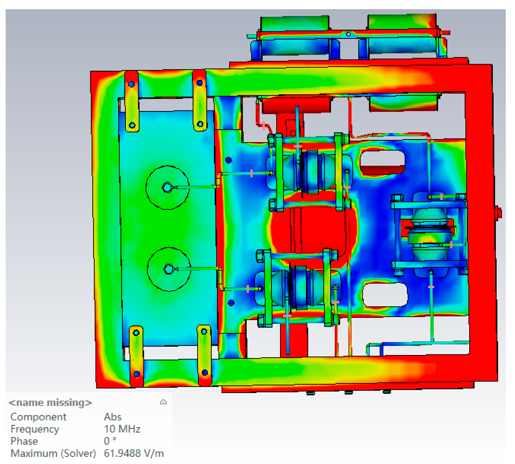
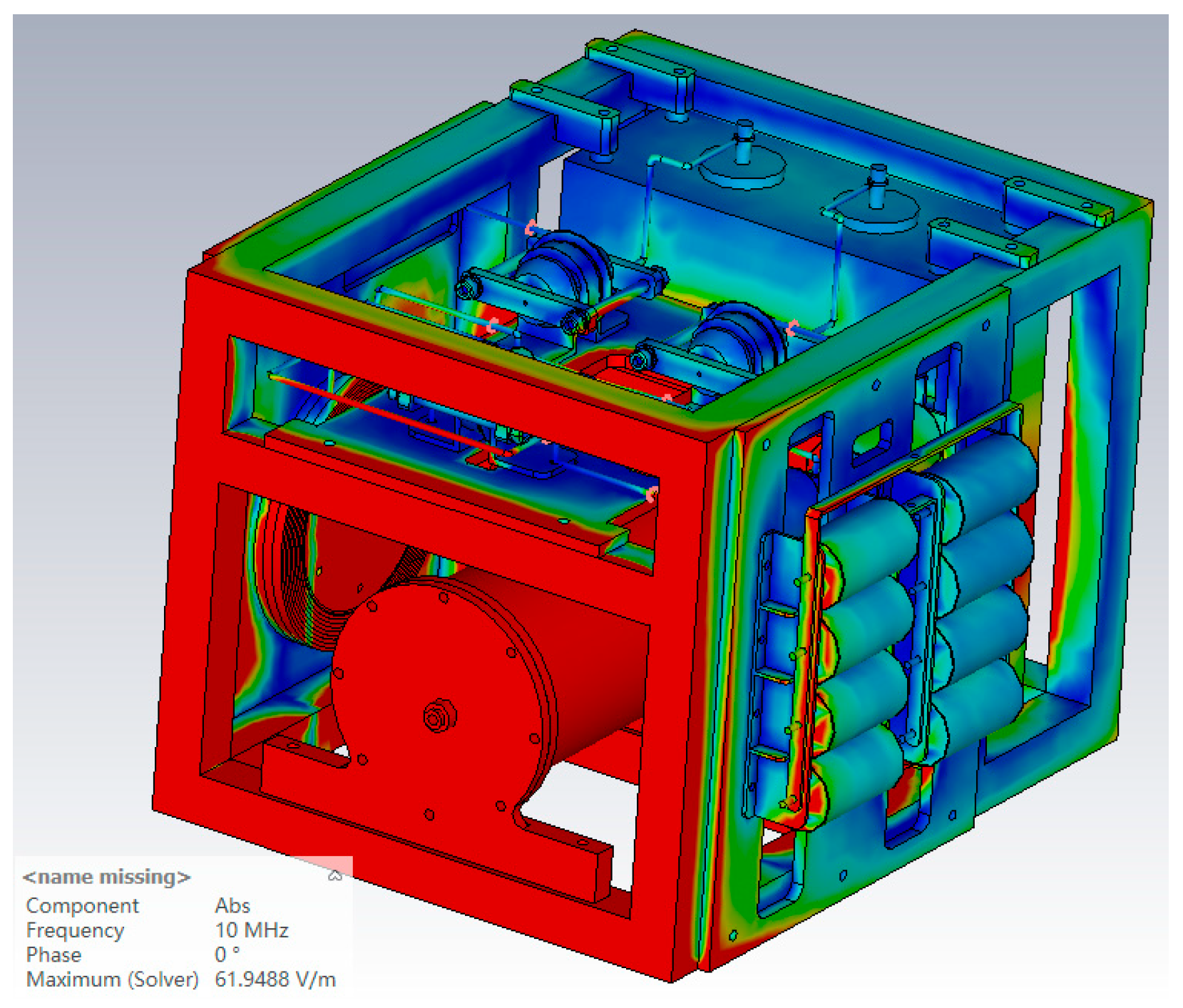
Figure 16 presents the full-wave electric field distribution of the whole machine at 10 MHz. The computational model integrates all structural components including metal chassis, transformers, energy storage capacitors, thyristor modules and internal connecting cables. The color scale of the cloud map indicates that red regions correspond to the maximum electric field strength of 61.9488 V/m, concentrated on transformer windings, unshielded outgoing cables and chassis gaps, which are the primary radiation leakage positions requiring priority shielding and filtering optimization.
Figure 15.
Electric field distribution simulation results of high-power microwave power supply system.
Figure 15.
Electric field distribution simulation results of high-power microwave power supply system.
5.3. Quantitative Analysis of Radiation from Unshielded Cables
Two groups of comparative simulations are carried out: fully shielded cables and unshielded cables. The maximum radiated field strength of shielded cables is only 4.28 V/m, while that of unshielded cables rises to 61.94 V/m (14.5 times higher). Unshielded cables drastically amplify overall radiated interference, and scattered spatial electric fields will disturb near-field probes and oscilloscopes, raising background noise and reducing EMI test accuracy. Therefore, the cables of the prototype are uniformly adjusted to shielded cables to reduce the impact on the control module
6. Conclusion
This paper establishes high-precision system-level high-frequency EMI models and completes quantitative calculations under three operating modes via CST field-circuit co-simulation, revealing the multi-source and multi-path EMI mechanism dominated by gas spark gap transients and non-ideal thyristor switching of PFN-Marx HPPD systems. Prototype test data are supplemented to validate the effectiveness of field-circuit co-modeling for EMC analysis of complex pulsed power systems. The radiation interference introduced by unshielded cables and its impact on test results are quantitatively analyzed. The research outputs provide quantifiable analytical methods for EMI suppression design of high-power microwave power supplies with important theoretical and engineering prospects. The proposed parasitic parameter extraction-based SPICE modeling and global EMC co-simulation method can reproduce interference waveforms and support sensitivity analysis and pre-research of suppression schemes, possessing better predictability and controllability than traditional empirical design approaches.
Author Contributions
Methodology, Ruiheng Zhang and Yuzhang Yuan.; software, Ruiheng Zhang; validation, Haitao Wang, Xuejun Pei, and Jin Meng.; formal analysis, Ruiheng Zhang; investigation, Ruiheng Zhang; writing—original draft preparation, Ruiheng Zhang; writing—review and editing, Yuzhang Yuan; All authors have read and agreed to the published version of the manuscript.
Funding
This work was supported by the National Natural Science Foundation of China under Grant 62401605.
Data Availability Statement
All data generated or analyzed during this study, including circuit simulation waveforms, CST full-wave electric field cloud diagrams, and prototype measured voltage curves, are fully included within the published article and its supplementary material. No additional external datasets are required to reproduce the results of this work.
Acknowledgments
The authors would especially like to thank Naval University of Engineering for providing an excellent academic research environment and a comprehensive scientific research training platform, and thank Qianyuan Laboratory for offering well-equipped experimental sites, high-power microwave testing facilities and relevant software and hardware conditions for this research.
Conflicts of Interest
The authors declare no conflicts of interest.
References
- K. Wen, L. Liang, Z. Zhang, and X. Yan, "High Power and High Repetition Frequency Nanosecond Marx Generator Based on Avalanche Transistor With Triggering Acceleration Circuit," IEEE Transactions on Power Electronics, pp. 1-14, 2025.
- X. Fang, Lin. Li, Liang Liu. Equivalent model of electromagnetic radiation induced by gas-gap switches in intense electron beam accelerator, 2013, 25(04): 1055-8. [CrossRef]
- S. Liu, J. Zhang, and Z. Zhang, "Review of high power compact pulse forming network-Marx generators," High Power Laser and Particle Beams, vol. 34, pp. 1-11, 2022. [CrossRef]
- Y. Wu and C. Feng, "A compact PFN-Marx repetitive pulsed power source," High Power Laser and Particle Beams, vol. 36, pp. 1-6, 2024. [CrossRef]
- F. Lassalle et al., "Development and Test of a 400-kV PFN Marx With Compactness and Rise Time Optimization," IEEE Transactions on Plasma Science, vol. 46, no. 10, pp. 3313-3319, 2018. [CrossRef]
- J. Benford and J. A. Swegle, High Power Microwaves. New York: USA:Taylor & Francis, 2007.pp.43-97.
- P. Lehmann, "Overview of the electric launch activities at the French-German Research Institute of Saint-Louis (ISL)," IEEE Transactions on Magnetics, vol. 39, no. 1, pp. 24-28, 2003. [CrossRef]
- H. D. Fair, "Electromagnetic launch science and technology in the United States enters a new era," IEEE Transactions on Magnetics, vol. 41, no. 1, pp. 158-164, 2005. [CrossRef]
- H. Heydari, V. Abbasi, and F. Faghihi, "Impact of Switching-Induced Electromagnetic Interference on Low-Voltage Cables in Substations," IEEE Transactions on Electromagnetic Compatibility, vol. 51, no. 4, pp. 937-944, 2009. [CrossRef]
- G. Zhang and R. Cao, "Comparison of Magnetic Field Characteristics Produced by Three-Electrode Spark Gap Switch and Thyristor Switch in Power Pulsed Systems," IEEE Transactions on Plasma Science, vol. 47, no. 11, pp. 5172-5179, 2019. [CrossRef]
- Siew, Howat, and Chalmers, "Radiated interference from a high voltage impulse generator," IEEE Transactions On Electromagnatic Compatibility, vol. 38, no. 4, pp. 600-604 1996. [CrossRef]
- X. Fan and J. Liu, "Research on the electromagnetic radiating during the operation of intense electron-beam accelerator," Laser and Particle Beams, vol. 31, no. 1, pp. 149-154, 2013. [CrossRef]
- A. R. G. V. Rao, A. S. Paithankar and P. H. Ron, "Electromagnetic interference by high power microwaves," presented at the Proceedings of the International Conference on Electromagnetic Interference and Compatibility, Bangalore, 2002.
- Y. Tao et al., "Prediction of Electromagnetic Pulse Radiation at High Power Laser Facility," presented at the 2022 IEEE 5th International Conference on Electronics Technology (ICET), Chengdu, 2022.
- A. Larsson, B. Johansson, and S. E. Nyholm, "Radiated electric field strength from high-power microwave systems," presented at the 2006 17th International Zurich Symposium on Electromagnetic Compatibility, Singapore, 2006.
- B. Cadilhon et al., "High Pulsed Power Sources for Broadband Radiation," IEEE Transactions on Plasma Science, vol. 38, no. 10, pp. 2593-2603, 2010. [CrossRef]
- Y. Guan, G. Yue, W. Chen, Z. Li, and W. Liu, "Experimental Research on Suppressing VFTO in GIS by Magnetic Rings," IEEE Transactions on Power Delivery, vol. 28, no. 4, pp. 2558-2565, 2013. [CrossRef]
Figure 1.
Topology diagram of high-power microwave system circuit.
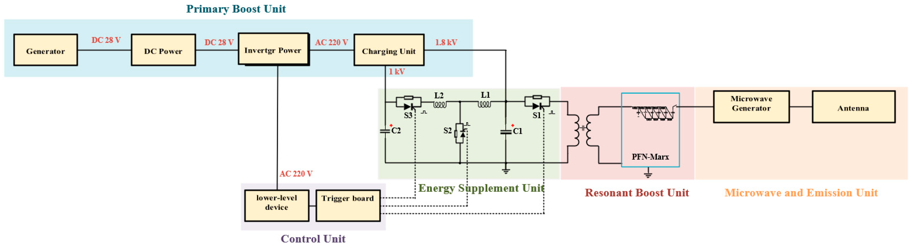
Figure 2.
Circuit topology diagram of operating condition 1.
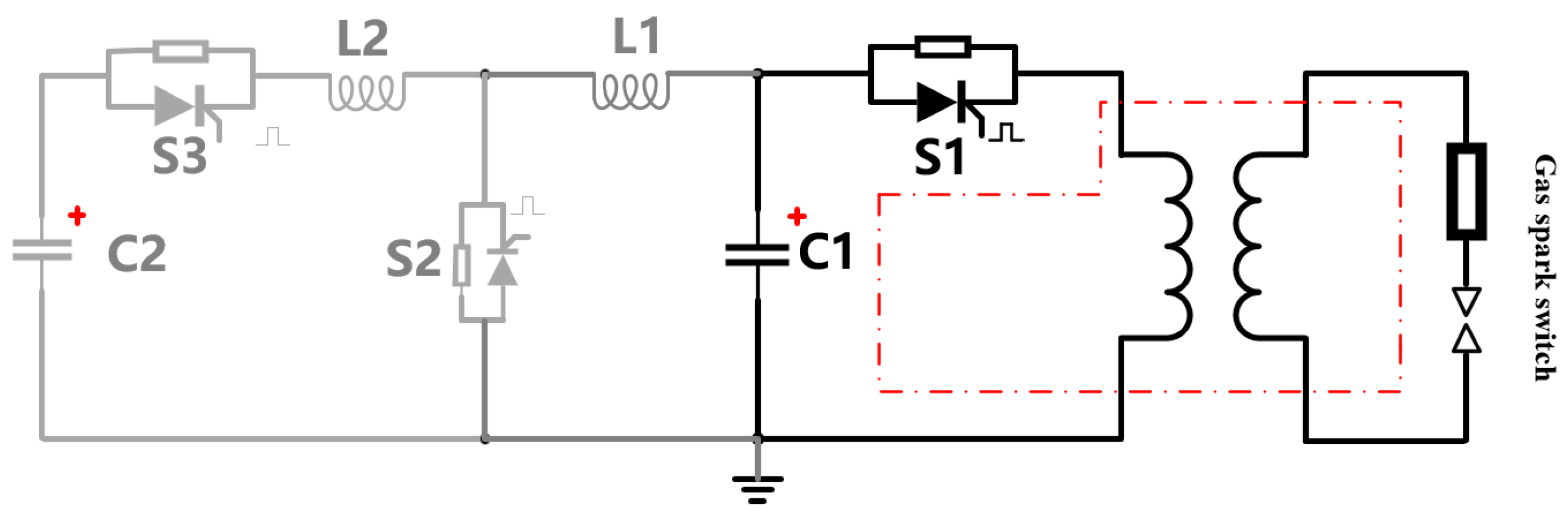
Figure 3.
Circuit topology diagram of operating condition 2.
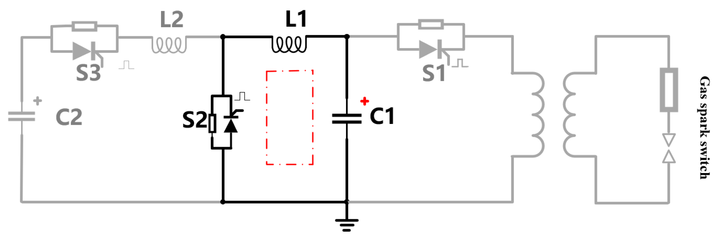
Figure 4.
Circuit topology diagram of working condition 3.
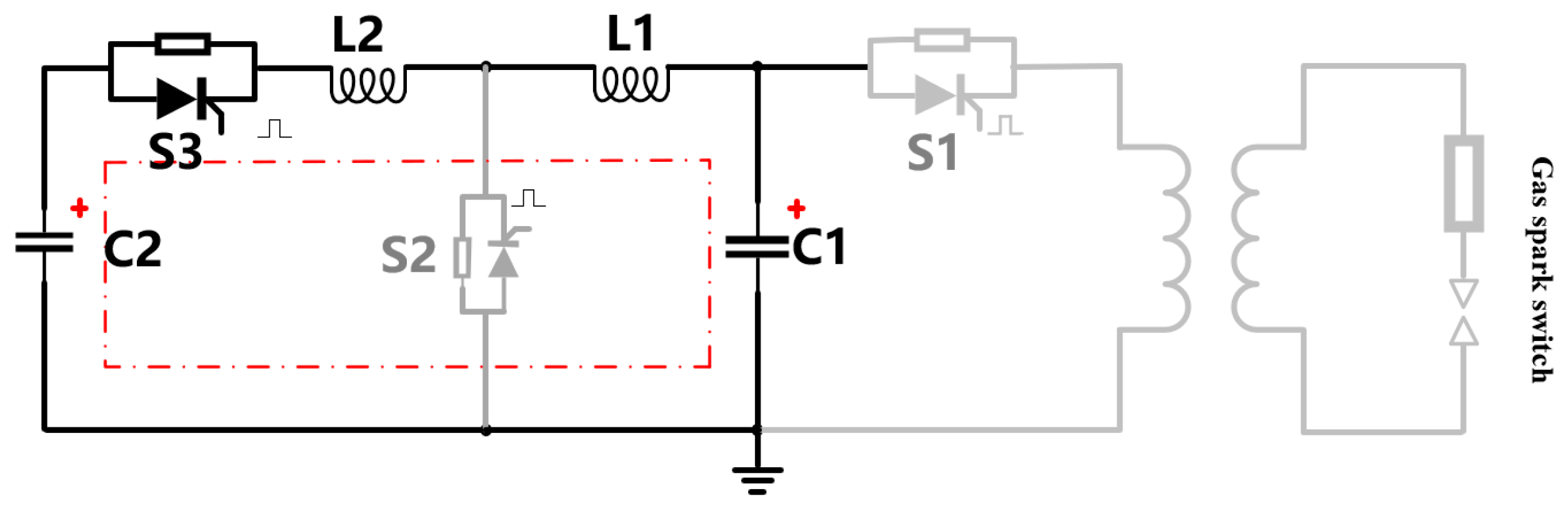
Figure 5.
Switch timing diagram.
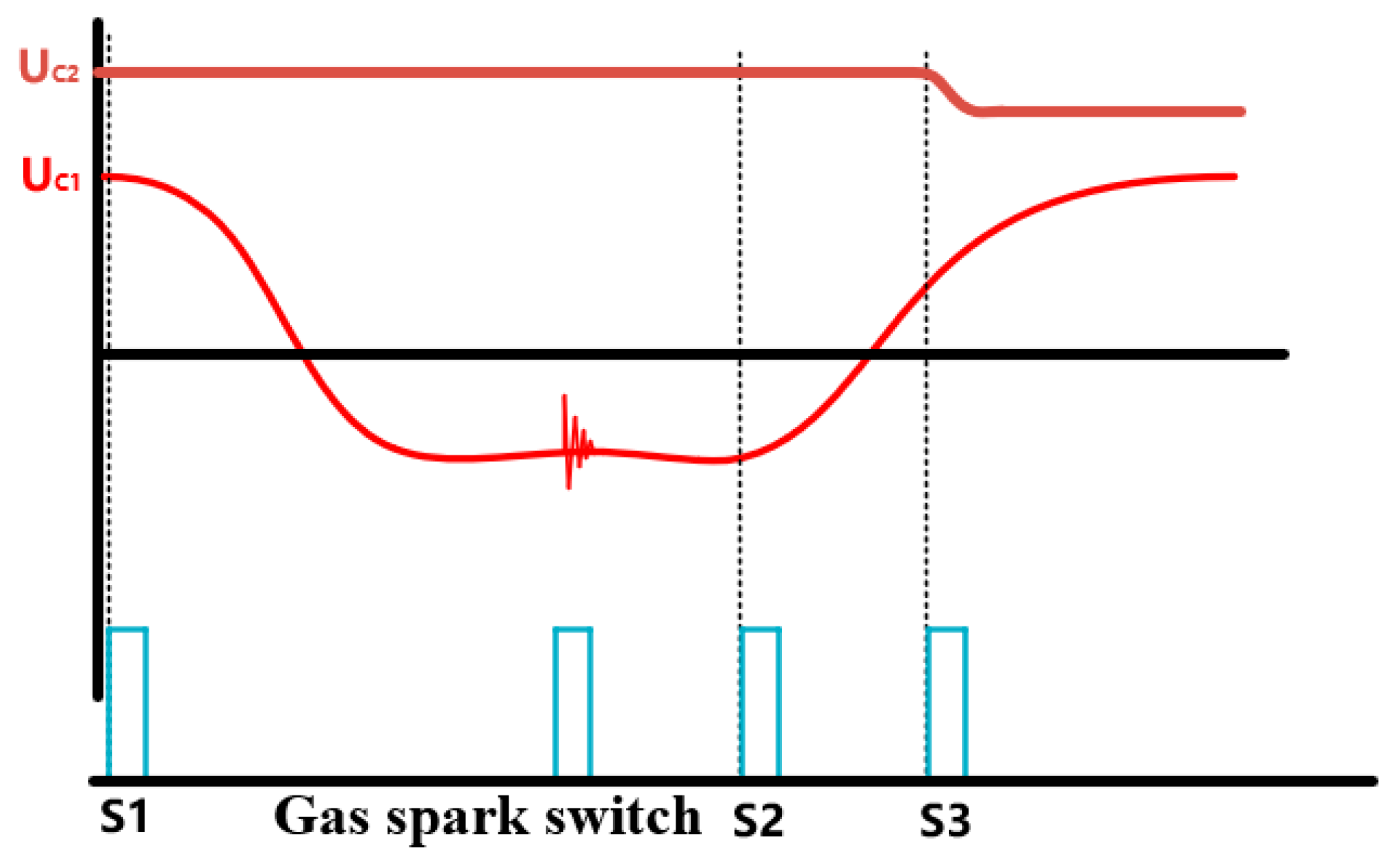
Figure 7.
Topology of PFN-Marx circuit.

Figure 9.
Equivalent Circuit Topology of Interference Mechanism.
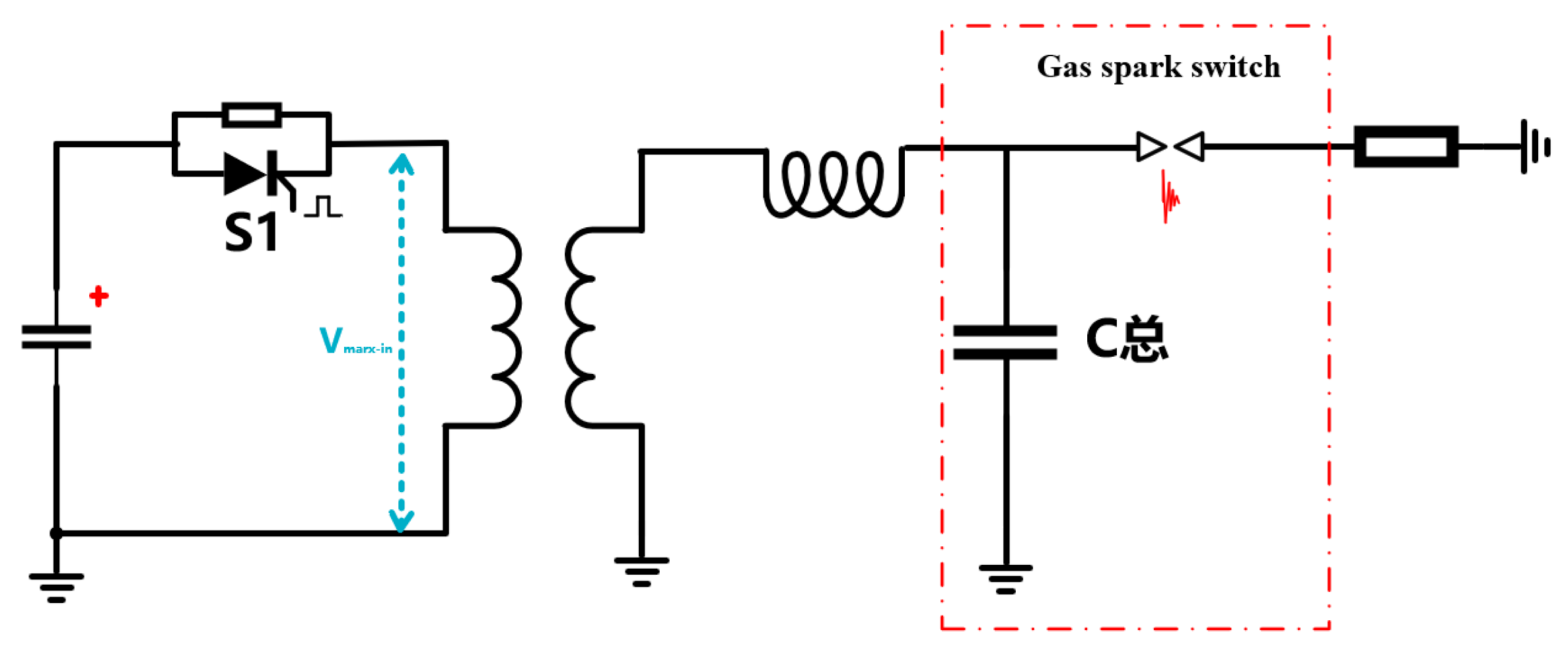
Figure 11.
High-frequency modeling of filtering inductors and capacitors.
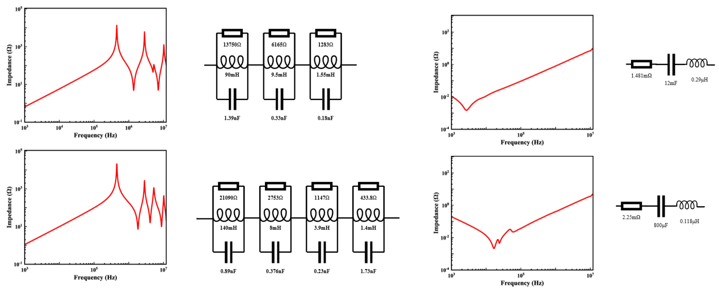
Figure 12.
Parasitic capacitance of thyristor.
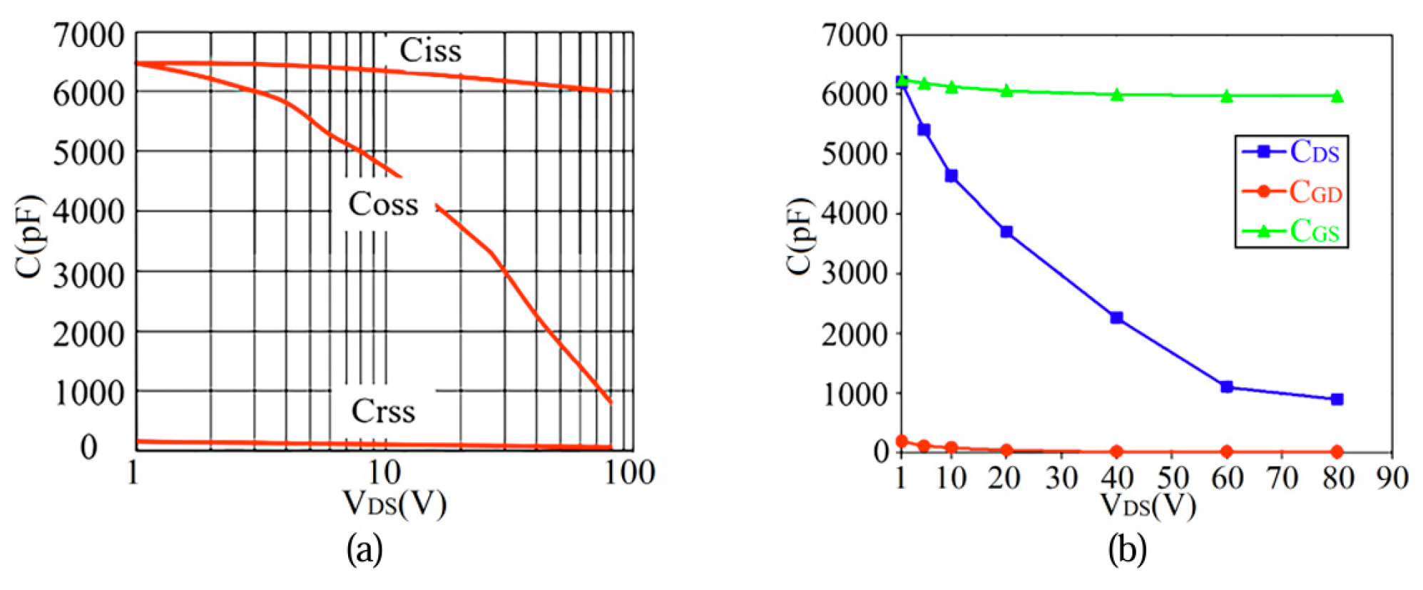
Figure 13.
Simulation diagram of high-power microwave system circuit.
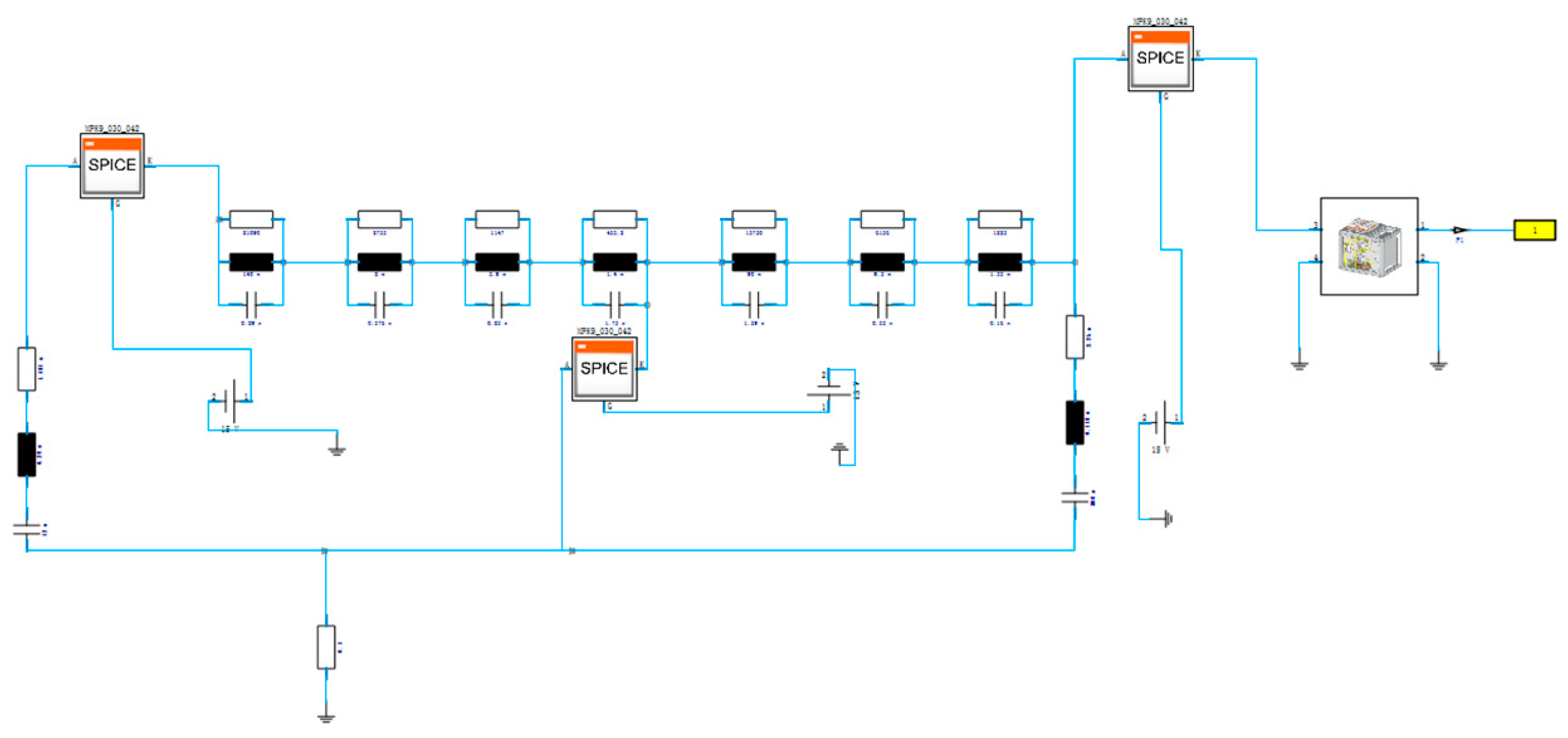

Table 1.
EMI characteristic parameters under three operating modes.
| Mode | Typical Performance | System Recovery Method | Dominant Interference Source |
| Mode 1 | 20 kV | 4200ns | Gas spark switch |
| Mode 2 | 1.1 kV | 2000ns | Thyristor S2 (spark gap coupling interference) |
Disclaimer/Publisher’s Note: The statements, opinions and data contained in all publications are solely those of the individual author(s) and contributor(s) and not of MDPI and/or the editor(s). MDPI and/or the editor(s) disclaim responsibility for any injury to people or property resulting from any ideas, methods, instructions or products referred to in the content. |
© 2026 by the authors. Licensee MDPI, Basel, Switzerland. This article is an open access article distributed under the terms and conditions of the Creative Commons Attribution (CC BY) license (http://creativecommons.org/licenses/by/4.0/).
Copyright: This open access article is published under a Creative Commons CC BY 4.0 license, which permit the free download, distribution, and reuse, provided that the author and preprint are cited in any reuse.


