

Submitted:
20 July 2026
Posted:
20 July 2026
You are already at the latest version
Abstract
In this study, Mo/β-Ga₂O₃ vertical Schottky barrier diodes (SBDs) were fabricated using a sputtering process, and the electrical characteristics were evaluated as a function of post-annealing temperature. β-Ga₂O₃ is an ultra-wide bandgap semiconductor (UWBG) with a bandgap of about 4.8 eV and a critical breakdown field of 8 MV/cm, a promising material for high-voltage power switching applications. Mo (molybdenum) has a higher work function (~4.95 eV) than the electron affinity (~4.0 eV) of β-Ga₂O₃, its melting point (2623°C) is higher than Pt (1768°C) and Ni (1455°C), so it has excellent thermal stability, and it is selected as Schottky metal. The device is a structure in which a Si-doped β-Ga₂O ₃ epitaxial layer (10μm, Nd–Na = 2.2 × 1016cm ⁻³) is grown on an Sn-doped β-Ga₂O ₃ substrate (415μm, Nd–Na = 4.5 × 10¹⁸ cm ⁻³). The Ti/Au (10/40 nm) was used for back ohmic junction and Mo (300 nm) was used for front Schottky junction. Post-annealing treatment was performed at 400, 500, and 550°C using a rapid-thermal annealing process (RTA) in an Ar gas atmosphere, and in this process, Schottky junction and ohmic junction were formed simultaneously. Electrical characteristics including current-voltage(I-V), capacitance-voltage(C-V), Schottky barrier height (SBH), ideality factor (n), turn-on voltage (Von), on-resistance (Ron), on/off ratio, and breakdown voltage (BV) were evaluated. No obvious Schottky characteristics were observed before post-annealing treatment, which means that As-deposited Mo does not form a rectifying junction on the β-Ga₂O₃ without post-annealing treatment. After post-annealing treatment, the I–V curve of the Schottky rectification characteristics could be confirmed under all three conditions. Among the three conditions, the device annealed at 500°C exhibits best performance, with SBH of 0.96 eV, n of 1.01, Von of 0.72 V, Ron of 13.8 mΩ·cm², an on/off ratio of 10⁹, a breakdown voltage of -474 V, and a PFOM of 16.3MW/cm2. As a result of temperature-dependent I–V measurement, as chuck temperature increased, the reverse leakage current increased and SBH decreased in all devices, which is consistent with the thermally activated carrier transport. These results demonstrate that the Mo/β-Ga₂O₃ SBDs are a thermally stable contact for power device applications.
Keywords:
β-Ga₂O₃
; molybdenum
; vertical Schottky barrier diodes
; post-annealing treatment
; power device
; sputtering
1. Introduction
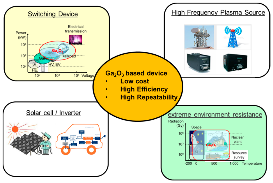
With the rapid development of power electronic systems such as electric vehicles, solar inverters, and high frequency power converters, demand for semiconductor devices capable of high voltage, high temperature, and high frequency operations is increasing. Existing silicon (Si)-based power devices have performance limitations due to narrow bandgap (1.1 eV) and low critical electric field value (0.3 MV/cm), and to overcome them, wide bandgap (WBG) semiconductors such as 4H-SiC (3.3 eV) and GaN (3.4 eV) are being used.[1,2,3,4] However, even this material has limitations in fully satisfying the requirements of ultra-high voltage and extreme environmental power systems. Gallium oxide, which belongs to ultra-wideband semiconductors, is receiving a lot of attention thanks to its excellent combination of material properties. The β-Ga₂O₃ has a theoretical critical breakdown field of 8 MV/cm with a band gap of about 4.8 eV, and the Baliga figure of merit (BFOM) of about 3,444, which is about 10 times that of SiC and about 4 times that of GaN.[1,2,3,4,22] One of the biggest practical advantages of β-Ga₂O₃ compared to competing ultra-wide bandgap (UWBG) materials such as AlN, diamond, and cubic boron nitride (c-BN) is the ability to fabricate large-area high-quality single crystal substrates with melt growth methods such as edge-defined film-fed growth (EFG) and Czochralski methods.[5] This substrate manufacturing method is suitable for industrial-scale production, enabling cost-effective wafer supply. In addition, n-type doping of β-Ga₂O₃ can be precisely controlled in a wide range from semi-insulating (Fe-doped) to highly conductive n-type (Nd–Na to 10¹⁹ cm ⁻³) (Sn-doped).[6] These properties make β-Ga₂O ₃ an attractive material for power device manufacturing compared to other UWBG candidate materials. Among the various β-Ga₂O ₃ rectification device structures, the Schottky Barrier Diode (SBD) is the most actively studied structure due to its fast switching speed and compatibility with a simple manufacturing process.[7] SBH, n(ideality Factor) , Ron, BV, and on/off ratio, which are the main performance parameters of SBDs, vary greatly in the Schottky metal-semiconductor junction. Schottky metals commonly used in the study of gallium oxide Schottky barrier diodes (SBD) include platinum (Pt), nickel (Ni), gold (Au), and tungsten (W), which generally have a Schottky barrier height (SBH) value in the range of 1.0 to 1.5 eV.[8,9,10,11] However, the Schottky junction between the above metal and gallium oxide exhibit low thermal stability under high-temperature operation or high-temperature post-annealing treatment conditions, which can lead to increased leakage current, reduced barrier height, and device failure.[12,13] Among the candidates for gallium oxide Schottky metal, molybdenum (Mo) has three key advantages. First, Mo has a work function of about 4.95 eV, which is higher than the electron affinity (about 4.0 eV) of n-type gallium oxide, satisfying the conditions required for Schottky barrier formation. Second, Mo's melting point is 2623°C, which is significantly higher than that of platinum (Pt, 1768°C) or nickel (Ni, 1455°C), providing excellent thermal stability against deterioration of the junction with gallium oxide during high-temperature heat treatment and device operation. Third, Mo has a relatively lower Schottky barrier height (SBH, about 0.96 eV) on gallium oxide compared to Pt or Ni-based bonding (1.0–1.5 eV), as demonstrated in a recent Mo/β-Ga₂O₃ SBD study, so it has a lower threshold voltage and higher rectification efficiency than Pt or Ni based devices. [1,23] Despite these advantages, Mo deposited by sputtering does not form a Schottky barrier by deposition alone, and a post-annealing treatment step is required to promote interfacial diffusion between Mo and the β-Ga₂O₃ surfaces to form a stable Schottky barrier. These thermally activated interface characteristics combined with the intrinsic properties of Mo to make Mo/Ga₂O₃ SBD suitable for highly reliable high temperature power device applications.[1,23] Existing studies have confirmed the possibility of Mo-based Schottky junction on β-Ga₂O₃, but systematic studies that combine the effect of post-annealing treatment temperature on electrical properties and temperature-dependent characteristic evaluation have not been sufficiently reported. Such a study is essential for evaluating the reliability of Mo/β-Ga₂O₃ SBD under actual operating conditions that can be exposed to high temperatures in extreme environments. In this study, Mo/β-Ga₂O₃ vertical SBDs were fabricated the post-annealing treatment temperatures (400°C, 500°C, 550°C) were systematically changed, and electrical characteristics including I–V, C–V, BV, and temperature dependence were evaluated.
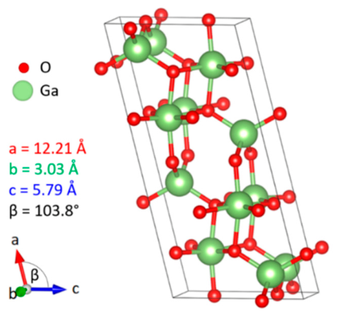

| Property | Value |
|---|---|
| Crystal structure | Monoclinic (space group C2/m) |
| Density | 5.95 x 10³ kg/m3 |
| Melting point | 1725°C |
| Refractive index | 1.97@450nm |
| Property | Si | 4H-SiC | GaN | β-Ga2O3 |
|---|---|---|---|---|
| Band gap Eg (eV) | 1.1 | 3.3 | 3.4 | 4.8 |
| Electron Mobility (cm2/V.s) | 1,400 | 1,000 | 1,200 | 200~300 |
| Critical electric field (MV/cm) | 0.3 | 2.5 | 3.3 | 8 |
| Baliga's Figure of Merit (BFOM) | 1 | 340 | 870 | 3,444 |
| Relative permittivity (εr) | 11.8 | 9.7 | 9.0 | 10 |
| Thermal conductivity (W/cm·K) | 1.5 | 4.9 | 1.3 | ~0.27 |
2. Materials and Methods
2.1. Structure and Materials
Mo (molybdenum) has a higher work function (~4.95 eV) than the electron affinity (~4.0 eV) of the β-Ga₂O₃, a higher melting point (2623°C) than Pt (1768°C) and Ni (1455°C), providing excellent thermal stability. In this study, the Mo/β-Ga₂O₃ vertical Schottky barrier diode was fabricated on a β-Ga₂O₃ epitaxial wafer. As shown in Figure 3 and Table 3, the substrate consists of a Si-doped β-Ga₂O₃ epitaxial layer grown on the Sn-doped β-Ga₂O₃ substrate. The Si-doped n-type epitaxial layer, which acts as a drift region, is 10 μm thick and has a carrier concentration (Nd–Na) of 2.2 × 10¹⁶cm⁻³. This relatively low doping in the drift layer enables high breakdown voltage allowing a wide depletion region to form under reverse bias. The Sn-doped n⁺ substrate has a thickness of 415 μm and a carrier concentration (Nd–Na) of 4.5×10¹⁸ cm⁻³, and a current flows vertically through the epitaxial layer from the front Schottky junction to the back ohmic junction allowing the entire drift layer to support the breakdown voltage. Mo (300 nm thick) was used as a Schottky metal layer for the front Schottky junction. The back ohmic junction was formed by depositing a Ti/Au double layer (Ti 10 nm / Au 40 nm) using E-beam evaporator.[13,14,16] The active area was 0.07 mm².
2.2. Fabrication Process Flow
As shown in Figure 4, to remove organic contaminants from the surface of the β-Ga₂O₃ wafer, ultrasonic cleaning was performed in acetone, IPA, and deionized water followed by drying (N2 )was performed thereon. In this cleaning process, it removes organic contaminants that could otherwise cause delamination. After cleaning the substrate, the plasma surface treatment was performed. The plasma treatment changes the surface energy of epitaxial layer for hydrophilic properties, and organic contaminants on epitaxial layer are removed to improve physical adhesion between a metal and an epitaxial layer. Then, Ti/Au back metal layer was deposited on a Sn-doped Ga₂O₃ substrate by using E-beam evaporator in a base pressure of 4×10⁻⁶ Torr. After then, Mo Schottky metal (300 nm thick) was deposited on the β-Ga₂O₃ epitaxial layer by using sputtering. Deposition was carried out at a pressure of 3mTorr and input power of 30 W at room temperature conditions in an Ar gas atmosphere. After Mo metal deposition, post-annealing treatment was performed at 400°C, 500°C, and 550°C for 1minute in a 100mTorr Ar atmosphere using a rapid Thermal Annealing (RTA) system. During RTA process, the Mo/ β-Ga₂O₃ Schottky junction and back Ti/Au ohmic junction were formed simultaneously. As-deposited Mo does not form a Schottky junction with the β-Ga₂O₃ epitaxial layer, but after post-annealing treatment process, Mo atoms are partially diffused into the β-Ga₂O₃ near-surface region forming a stable Schottky junction.[23,24] The post-annealing temperatures were selected to investigate their effect on the Schottky barrier height and electrical properties of the device.
2.3. Electrical Properties
After device fabrication, the electrical characteristics of the Mo/β-Ga₂O₃ SBD were evaluated using a Keithley 4200 semiconductor parameter analyzer and an LCR meter. I–V characteristics were measured under both forward and reverse bias to extract the main device parameters. Forward I–V characteristics were analyzed using a thermionic emission (TE) model which describes current transport across the Schottky barrier. [2,10,11,12] According to the TE model, the current density is given by a diode equation:
The reverse saturation current density (J₀) is a constant that determines the magnitude of a small leakage current flowing when a diode is in a reverse bias state. A* is the effective Richardson constant, T is the temperature, q is the electron charge, ΦB is the Schottky barrier height, k is the Boltzmann constant, n is the ideality factor, and V is the voltage. Schottky barrier heights (SBH, ΦB) were using a Richardson plot and were also estimated from C–V curve [9,10,11]
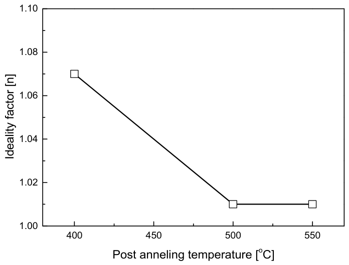
The ideality factor (n) was extracted from the slope of the ln (J) vs. V plot in the forward region. Closer to n=1 indicates the ideal thermionic emission(TE) behavior with a defect-free Schottky barrier, where n > 1 indicates the interfacial state, barrier non-uniformity, or the presence of non-ideal current transfer mechanisms such as recombination or tunneling.[9,10,11] The turn-on voltage (Von) was extracted by linear extrapolation of the forward I–V curve, and the on-resistance (Ron) was calculated from the linear region slope of the forward I–V curve at an applied voltage of +2V. The capacitance-voltage (C–V) characteristic was measured at 100 kHz frequency at room temperature. Built-in voltage (Vbi) and depletion width were measured using a 1/C² - V(Mott-Schottky) plot. The breakdown voltage (BV) was measured by sweeping the reverse voltage until the current reached the set compliance limit. The thermal stability of the Schottky junction under high-temperature operating conditions was evaluated by performing temperature dependent I-V measurement while changing the chuck temperature for the post-annealing device at 500°C and 550°C.
3. Results
3.1. Schottky Junction Formation Mechanism and Effect of Post-Annealing Temperature
As shown in Figure 5(a) and (b), the as-deposited Mo/β-Ga₂O₃ structure did not exhibit rectified I–V properties, indicating that Mo thin film does not form Schottky junction on the β-Ga₂O₃ surface immediately after deposition. This is attributed to plasma-induced damage and surface defects generated during deposition, which create a high density of interface states and lead to Fermi-level pinning, thereby suppressing the formation of the Schottky barrier.[7,23] After post-annealing at 400, 500, and 550°C, rectified I–V characteristics were observed in all devices, confirming that a Schottky junction has been formed. In the RTA process, Mo atoms partially diffuse into the β-Ga₂O₃ interface, modifying the interfacial properties and thereby promoting the formation of stable Schottky junction. As summarized in Table 4, the post-annealing temperature had a significant effect on the diode characteristics. The device at 500°C exhibited the best overall performance. It showed the highest SBH (0.96 eV), the lowest ideality factor (n = 1.01), highest Von (0.72V), and the highest on/off ratio (10⁹). The ideality factor (n) close to unity obtained at 500°C indicates that thermionic emission (TE) is the dominant charge transport mechanism. [2,10,11,12] In addition, these results suggest that the interfacial defect density is low and a spatially uniform Schottky junction is formed. On the other hand, a high on/off current ratio of about 10⁹ reflects excellent rectification characteristics, which supports its applicability as a power switching device. The device annealed at 400°C showed a low SBH (0.92 eV) and a high ideality factor (n=1.07). When n is higher than the optimal post-annealing treatment temperature, it is determined that diffusion of Mo into β-Ga₂O₃ Epitaxial layer is not sufficient. However, device annealed at 550°C resulted in rather deteriorating device performance. The ideality factor was n=1.01, which approached an ideal value, but the on/off current ratio was reduced to 10⁸, and the Ron was increased to 22.4 mΩ·cm². This is approximately1.6 times higher than the Ron at 500°C, indicating that excessive annealing temperature degrades device performance. This degradation is due to excessive Mo diffusion at 550°C and the generation of interface defects, which increases contact resistance by reducing the effective doping concentration of the epitaxial layer near the interface. As shown in Figure 6, The breakdown voltage (BV) also decreased from - 474 V at 500°C to -419 V at 550°C, which is attributed to an increase in interfacial trap density caused by excessive annealing, resulting in a decrease in breakdown characteristics. Meanwhile, the turn-on voltage (Von) decreased to 0.67V at 550°C compared to 500°C, which is consistent with the slight decrease in the SBH from 0.96 eV to 0.93 eV. These results suggest that the Mo/β-Ga₂O₃ interfacial Schottky barrier was partially degraded by excessive Mo diffusion and interfacial defect formation at the highest annealing temperature.[23]
Figure 5.
a). Forward and reverse I–V characteristics of Mo/β-Ga₂O₃ SBDs annealed at RT, 400°C, 500°C, and 550°C (Log Scale).
Figure 5.
a). Forward and reverse I–V characteristics of Mo/β-Ga₂O₃ SBDs annealed at RT, 400°C, 500°C, and 550°C (Log Scale).
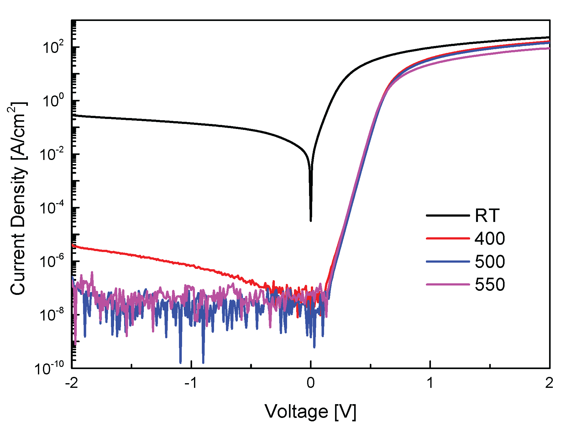
Figure 5.
b). Forward and reverse I–V characteristics of Mo/β-Ga₂O₃ SBDs annealed at RT, 400°C, 500°C, and 550°C. (linear Scale).
Figure 5.
b). Forward and reverse I–V characteristics of Mo/β-Ga₂O₃ SBDs annealed at RT, 400°C, 500°C, and 550°C. (linear Scale).
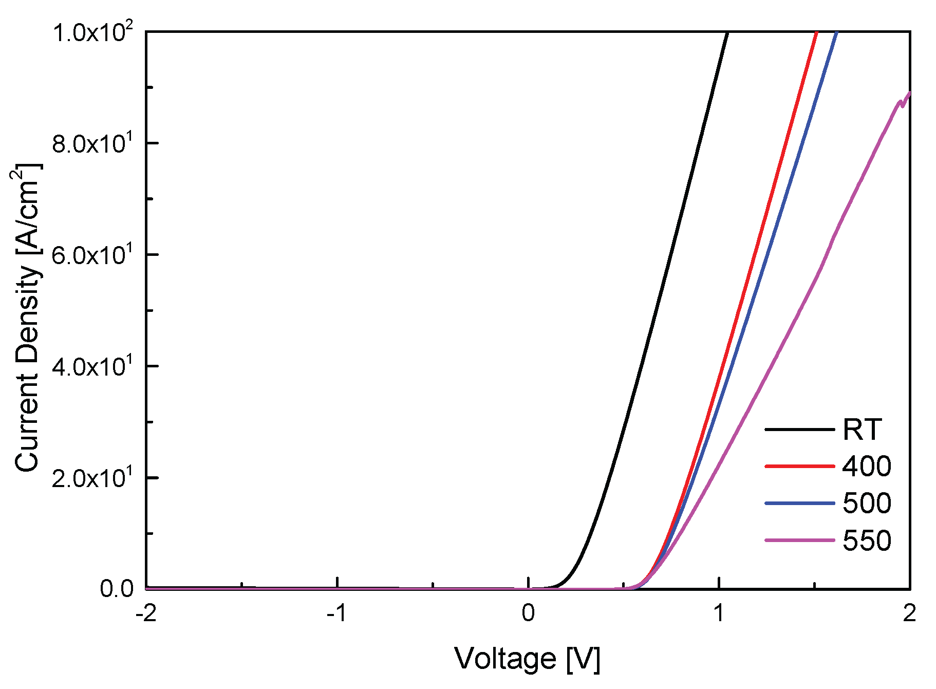
Figure 6.
Reverse breakdown voltage characteristics of Mo/β-Ga₂O₃ SBDs annealed at 500°C and 550°C.
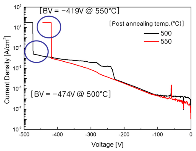
Figure 7.
Electrical parameters of Mo/β-Ga₂O₃ SBDs as a function of post-annealing temperature.
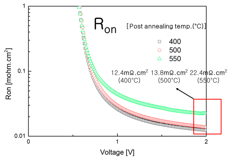
Table 4.
Electrical parameters of Mo/β-Ga₂O₃ SBDs as a function of post-annealing temperature (room temperature measurement).
Table 4.
Electrical parameters of Mo/β-Ga₂O₃ SBDs as a function of post-annealing temperature (room temperature measurement).
| Post annealing Temp.[℃] | |||
|---|---|---|---|
| ITEM | 400[℃] | 500[℃] | 550[℃] |
| SBH [eV] | 0.92 | 0.96 | 0.93 |
| n | 1.07 | 1.01 | 1.01 |
| Von [V] | 0.66 | 0.72 | 0.67 |
| Ron@2V [mΩ.cm2] | 12.4 | 13.8 | 22.4 |
| On/off Ratio | 109 | 109 | 108 |
Figure 8.
Schottky barrier height (SBH) of Mo/β-Ga₂O₃ SBDs annealed at 400°C, 500°C, and 550°C.
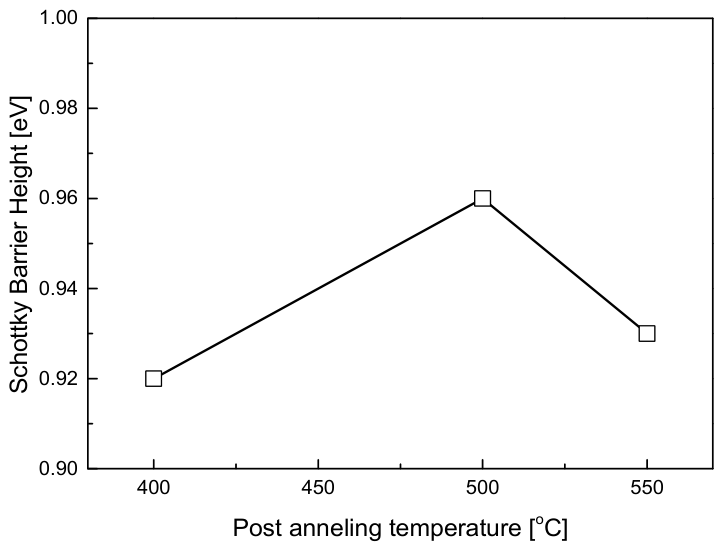
Figure 9.
Specific on-resistance (Ron,sp) of Mo/β-Ga₂O₃ SBDs annealed at 400°C, 500°C, and 550°C.
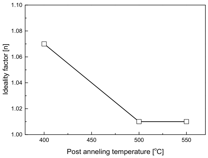
Figure 10.
Ideality factor (n) of Mo/β-Ga₂O₃ SBDs annealed at 400°C, 500°C, and 550°C.
3.2. C–V and 1/C²–V Analysis
In this study, C–V measurements were performed at a frequency of 100 kHz. The C–V characteristics showed a tendency for capacitance to decrease with increasing reverse bias, consistent with the depletion behavior of Schottky junction in which the depletion region extends into the lightly doped drift layer. In the reverse-bias section, the 1/C2 vs. V (Mott–Schottky) plot exhibited excellent linearity, confirming uniform doping of the drift layer and successful formation of the Schottky junction.[10,11] As shown in Figure 11, the built-in potential (Vbi) was extracted from the x-intercept of the 1/C2-V plot. Vbi exhibited 0.946V at 500℃ and 0.916V at 550℃. As shown in Figure 12, the depletion layer thickness was calculated from the C–V measurement results. The relative dielectric constant of β-Ga₂O₃ along the (001) direction (εᵣ= 12.4) was reported by Fiedler et al.[15] was applied in the calculation,
the depletion layer thickness under the zero-bias condition (V = 0 V) was 0.150 μm and 0.153 μm, at 500℃ and 550℃ respectively.
3.3. Temperature-Dependent Electrical Characteristics
In order to evaluate the thermal stability of the Mo/β-Ga₂O ₃ SBD, temperature-dependent current-voltage (I–V) characteristics were measured for devices at 500°C and 550°C. As shown in Figure 13(a,b) and Figure 14(a,b), I–V characteristics were measured under each post-annealing temperature condition while the chuck temperature was increased gradually from room temperature (~25°C) to 100°C. For both post-annealing treatment conditions, it was observed that the reverse leakage current tended to increase as the chuck temperature increased, consistent with the thermionic emission (TE) model, which predicts that the reverse saturation current density increases exponentially with temperature. [10,11,12] A comparison of the two post-annealing treatment conditions showed that the device at 500°C maintained superior electrical characteristics over the entire measurement temperature range. Specifically, the 500°C device exhibited a higher SBH and lower reverse leakage current than the 550°C device at all chuck temperatures, indicating relatively better thermal stability. It is judged that this is because of the Mo/β-Ga₂O₃ interface is more clearly defined in the 500℃ post-annealing treatment condition, and a spatially uniform barrier distribution is formed. On the other hand, it is analyzed that excessive heat treatment at 550℃ causes interfacial degradation or generation of additional defects, thereby lowering the high-temperature operation stability of the device. This temperature dependence of SBH is a phenomenon commonly reported in Schottky diodes and is due to the following complex mechanism. First, the height of the effective barrier detected by the carrier changes due to the temperature-dependent activation of the interface state near the Schottky barrier. Second, the effect of image-force lowering is strengthened by increasing the interface electric field according to the increase of the reverse bias. Third, due to the spatial non-uniformity of the barrier distribution across the entire metal-semiconductor junction, the thermally activated carrier selectively passes through the low barrier region, and as a result, the apparent SBH extracted from the I-V analysis tends to decrease with increasing temperature. [10,11,21]
3.4. Power Device Performance Evaluation
The breakdown voltage (BV) is the maximum reverse voltage that the device can withstand and is one of the key performance indicators for power devices. The 500°C post-annealing treatment device achieved BV = -474 V, which was improved by about 13% compared to -419 V for the 550°C device, indicating superior reverse-blocking characteristics. The Power figure-of-merit (PFOM = BV²/Ron) is a widely used indicator for evaluating the performance of unipolar power rectification devices.[2,7,22] For 500°C post-annealing treatment device, it was calculated as PFOM = (474)² / (13.8 × 10⁻³ Ω·cm²) ≈ 16.3 MW/cm² without an edge termination structure, suggesting that there is room for performance improvement when introducing the termination structure.[17,18,19,20]
4. Discussion
In this study, Mo Schottky metal was deposited on β-Ga₂O₃ epitaxial layer using sputtering equipment. Mo/β-Ga₂O₃ vertical Schottky barrier diode (SBD) was fabricated by rapid thermal annealing (RTA) in an Ar gas atmosphere. Electrical characteristics including I–V, C–V, breakdown voltage(BV), and temperature-dependent characteristics were evaluated. As-deposited Mo/β-Ga₂O₃ SBD did not exhibit Schottky rectification characteristics, and Schottky junction was formed after annealing at 400, 500, 550°C. The device at 500°C showed SBH=0.96 eV, n=1.01, Von=0.72 V, Ron=13.8 mΩ·cm², on/off current ratio =10⁹, and breakdown voltage BV= -474 V, indicating best performance among post-annealing treatment conditions. In particular, it was confirmed that high-quality Schottky junction was formed under the conditions by showing a value close to the ideality factor close to unity. On the other hand, excessive annealing treatment at 550°C caused excessive Mo diffusion, increasing Ron to 22.4 mΩ·cm², reducing the on/off current ratio to 10⁸, and lowering the BV to -419 V. As a result of temperature-dependent I–V measurements, the reverse leakage current systematically increased and SBH decreased with increasing chuck temperature in both 500 and 550°C post-annealing treatment. The 500°C annealed device exhibited higher SBH and lower leakage current over the entire measurement temperature range, and better thermal stability compared to the 550°C device. The power-figure of merit (PFOM=BV²/Ron) of the 500°C annealed device was calculated as about 16.3 MW/cm², demonstrating competitive performance for a β-Ga₂O₃ vertical SBD even without edge termination or passivation. These results confirm that the Mo metal deposited by the sputtering is a suitable Schottky junction material for the β-Ga₂O₃ based SBD, and clearly suggest that 500°C with Ar atmosphere condition is an post-annealing treatment condition that optimizes the device performance.
Funding
This research received no external funding.
Institutional Review Board Statement
Not applicable.
Informed Consent Statement
Not applicable.
Data Availability Statement
The original contributions presented in this study are included in the article. Further inquiries can be directed to the corresponding author.
Conflicts of Interest
Authors declare no conflict of interest.
References
- Hu, Z.; Feng, Z.; Cai, Y.; Shen, Y.; Yan, G.; Lu,X.;Zhang,C.;Zhou,H.;Zhang,J. Experimental and Theoretical Studies of Mo/Au Schottky Contact on Mechanically Exfoliated β- Ga2O3 Thin Film. Nanoscale Research Letter. 2019, 14, 2.
- Pearton, S.J.; Yang, J.; Cary, P.H.; Ren, F.; Kim, J.; Tadjer, M.J.; Mastro, A review of Ga2O3 materials, processing, and devices. M.A. Appl. Phys. Rev. 2018, 5, 011301.
- Higashiwaki, M.; Sasaki, K.; Murakami, H.; Kumagai, Y.; Koukitu, A.; Kuramata, A.; Masui, T.; Yamakoshi, S. Recent progress in Ga2O3 power electronics. Semicond. Sci. Technol. 2016, 31, 034001.
- Green, A.; Speck, J.; Xing, G.; Moens, P.; Allerstam, F.; Gumaelius, K.; Neyer, T.; Purdue, A.; Mehrotra, V.; Kuramata, A.; Sasaki, K.; Watanabe, S.; Koshi, K.; Blevins, J.; Bierwagen, O.; Krishnamoorthy, S.; Leedy, Kevin.; Arehart, A.; Neal, A.; Mou, S.; Ringel, S.; Kumar, A.; Sharma, A.; Ghosh, K.; Singisetti, U.;Li, W.; Chabak, K.; Liddy, K.; Islam, A.; Rajan, S.; Graham, S.; Chio, S.; Cheng, Z.; Higashiwaki, M.; β- Gallium oxide power electronics. APL Mater. 2022, 10, 029201.
- Galazka, Z.; Growth of bulk β- Ga2O3 single crystals by the Czochralski method. J. Appl. Phys. 2022, 131, 031103.
- Zhang, J.; Shi, J.; Qi, D.; Chen, L.; Zhang, K.H.L.; Recent progress on the electronic structure, defect, and doping properties of Ga2O3. APL Mater. 2020, 8, 020906.
- He, Y.; Zhao, F.; Huang, B.; Zhang, T.; Zhu, H.; A Review of β-Ga2O3 Power Diodes. Materials, 2024, 17, 1870.
- Farzana, E.; Zhang, Z.; Paul, P.K.; Arehart, A.R.; Ringel, S.A. Influence of metal choice on (010) β-Ga2O3 Schottky diode properties. Appl. Phys. Lett. 2017, 110, 202102.
- Mohamed, H.F.; Irmscher, K.; Janowitz, C.; Galazka, Z.; Manzke, R.; Fornari, R. Schottky barrier height of Au on the transparent semiconducting oxide β- Ga2O3. Appl. Phys. Lett. 2012, 101, 132106.
- Sheoran, H.; Tak, B.R.; Manikanthababu, N.; Singh, R.; Temperature-Dependent Electrical Characteristics of Ni/Au Vertical Schottky Barrier Diodes on β- Ga2O3 Epilayers. ECS J. Solid State Sci. Technol. 2020, 9, 055004.
- Yang, T.; Fu,H.; Chen, H.; Huang,X.; Montes, J.; Baranowski, I.; Fu, K.; Zhao, Y.; Temperature-dependent electrical properties of β-Ga2O3 Schottky barrier diodes on highly doped single-crystal substrates. J. Semicond. 2019, 40, 012801.
- Heinselman, K.; Walker, P.; Norman, A.; Parilla. P.; Ginley, D.; Zakutayev,A.; Performance and reliability of β- Ga2O3 Schottky barrier diodes at high temperature. J. Vac. Sci. Technol. A 2021, 39, 040402.
- Lee, M.; Chou, T.; Anooz, S.; Galazka, Z.; Popp, A.; Peterson, R.; Effect of post-metallization anneal on (100) Ga2O3 /Ti-Au ohmic contact performance and interfacial degradation. APL Mater. 2022, 10, 091105.
- Lyle, L.; Back, T.; Bowers, C.; Green, A.; Chabak, K.; Dorsey, D.; Heller, E.; Porter, L.; Electrical and chemical analysis of Ti/Au contacts to β- Ga2O3. APL Mater. 2021, 9, 061104.
- Fiedler, A.; Schewski, R.; Galazka, Z.; Irmscher, K. Static dielectric constant of β- Ga2O3 perpendicular to the principal planes (100), (010), and (001). ECS J. Solid State Sci. Technol. 2019, 8, Q3083.
- Carey, P.H.; Yang, J.; Ren, F.; Hays, D.C.; Pearton, S.J.; Jang, S.; Kuramata, A.; Kravchenko, I.I. Ohmic contacts on n-type β- Ga2O3 using AZO/Ti/Au. AIP Adv. 2017, 7, 095313.
- Roy, S.; Bhattacharyya, A.; Peterson, C.; Krishnamoorthy, S. 2.1 kV (001)- β- Ga2O3 vertical Schottky barrier diode with high-k oxide field plate. Appl. Phys. Lett. 2023, 122, 152101.
- Li, W.; Saraswat, D.; Long, Y.; Nomoto, K.; Jena, D.; Xing, H.G. Near-ideal reverse leakage current and practical maximum electric field in β- Ga2O3 Schottky barrier diodes. Appl. Phys. Lett. 2020, 116, 192101.
- He, Q.; Hao, W.; Zhou, X.; Li, Y.; Zhou, K.; Chen, C.; Over 1 GW/cm2 Vertical Ga2O3 Schottky Barrier Diodes Without Edge Termination. IEEE Electron Device Lett. 2022, 43, 264–267.
- Zhou, X.; Yang, J.; Zhang, H.; Liu, Y.; Xie, G.; Liu, W. A 1.6 kV Ga2O3 Schottky barrier diode with a low reverse current of 1.2 x 10⁻⁵A/cm2 enabled by field plates and N ion-implantation edge termination. Nanomaterials 2024, 14, 978.
- Werner, J.; Güttler, H.; Barrier inhomogeneities at Schottky contacts. J. Appl. Phys. 1991. 69, 1522–1533.
- Baliga. B. J, Power semiconductor device figure of merit for high-frequency applications, IEEE Electron Device Letters, 1989, 10, 455–457.
- Shiva, Sharma, N.; Kumar, M.; Kumar, M.; Low resistance ohmic contact of multi-metallic Mo/Al/Au stack with ultra-wide bandgap Ga2O3 thin film with post-annealing and its in-depth interface studies for next-generation high-power devices. J. Surfin. 2024. 46. 103937.
- Sheoran, H.; Kumar, V.; Singh, R.; A Comprehensive Review On Recent Developments in Ohmic and Schottky Contacts On Ga2O3 For Device Applications, ACS Appl. Electron. Mater. 2022, 4, 2589–2628.
Figure 3.
Schematic cross-sectional view of the Mo/β-Ga₂O₃ vertical Schottky barrier diode.
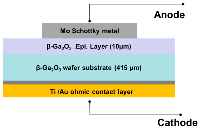
Figure 4.
Fabrication process flow of the Mo/β-Ga₂O₃ vertical Schottky barrier diode.
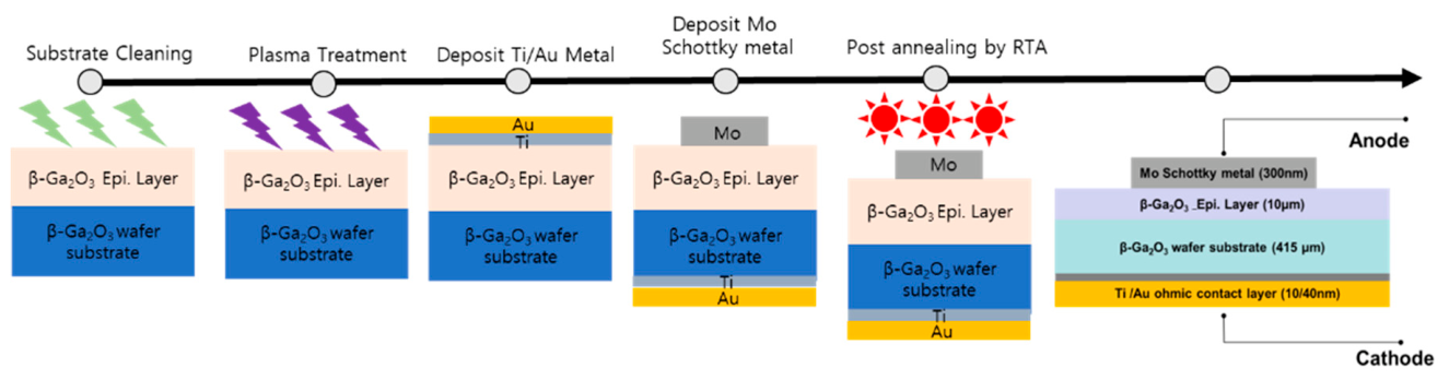
Figure 11.
(a) C–V characteristics and (b) Mott–Schottky (1/C² vs. V) plots of Mo/β-Ga₂O₃ SBDs measured at 100 kHz at room temperature.
Figure 11.
(a) C–V characteristics and (b) Mott–Schottky (1/C² vs. V) plots of Mo/β-Ga₂O₃ SBDs measured at 100 kHz at room temperature.
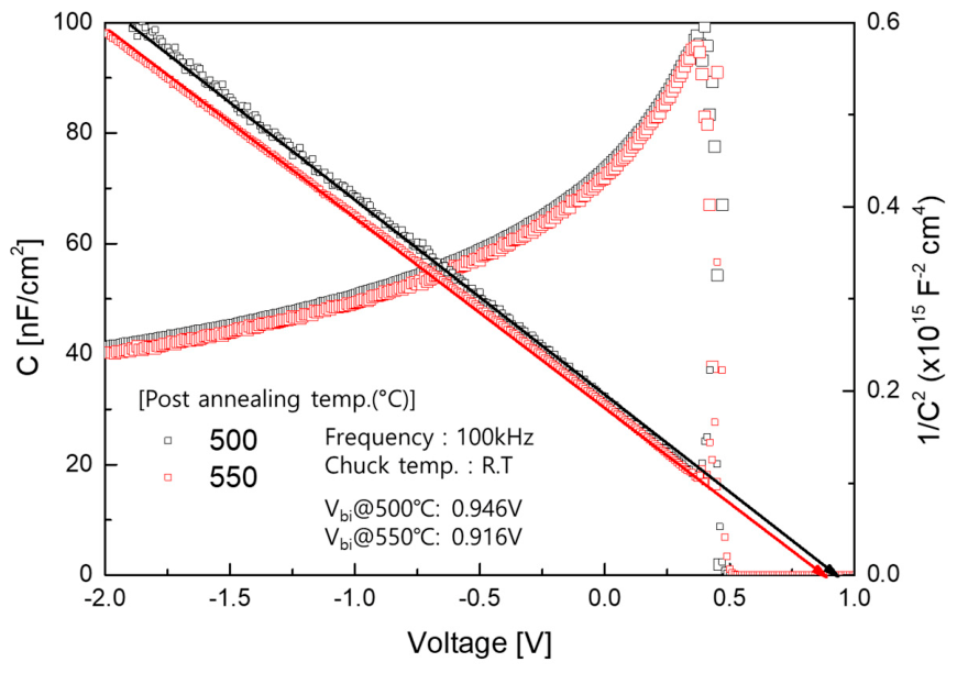
Figure 12.
Depletion width as a function of applied voltage for Mo/β-Ga₂O₃ SBDs measured at 100 kHz at room temperature.
Figure 12.
Depletion width as a function of applied voltage for Mo/β-Ga₂O₃ SBDs measured at 100 kHz at room temperature.
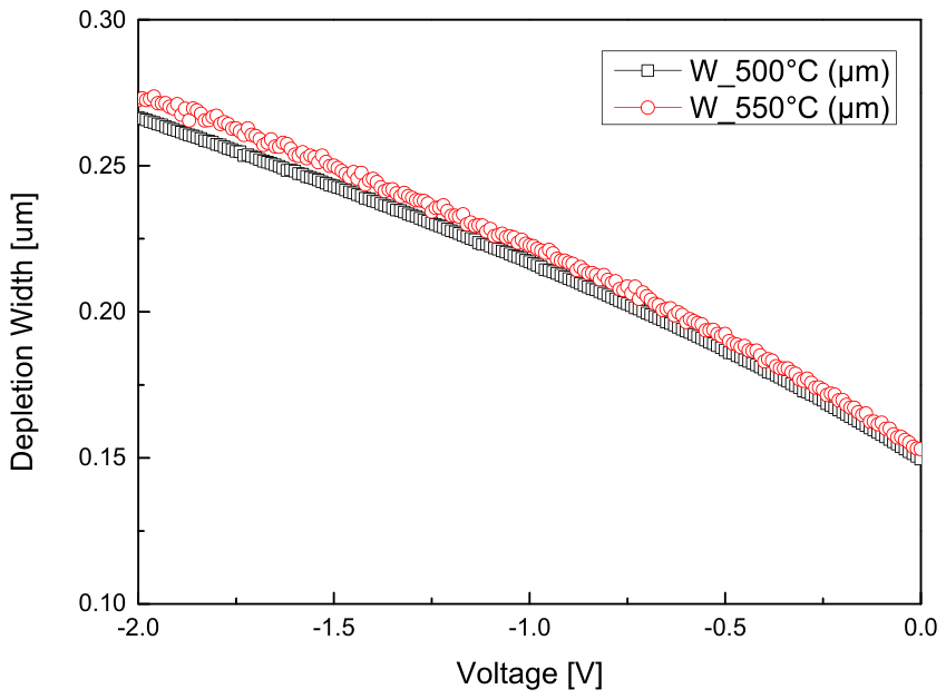
Figure 13.
Temperature-dependent I–V characteristics of Mo/β-Ga₂O₃ SBDs annealed at 500°C: (a) forward and (b) reverse bias.
Figure 13.
Temperature-dependent I–V characteristics of Mo/β-Ga₂O₃ SBDs annealed at 500°C: (a) forward and (b) reverse bias.
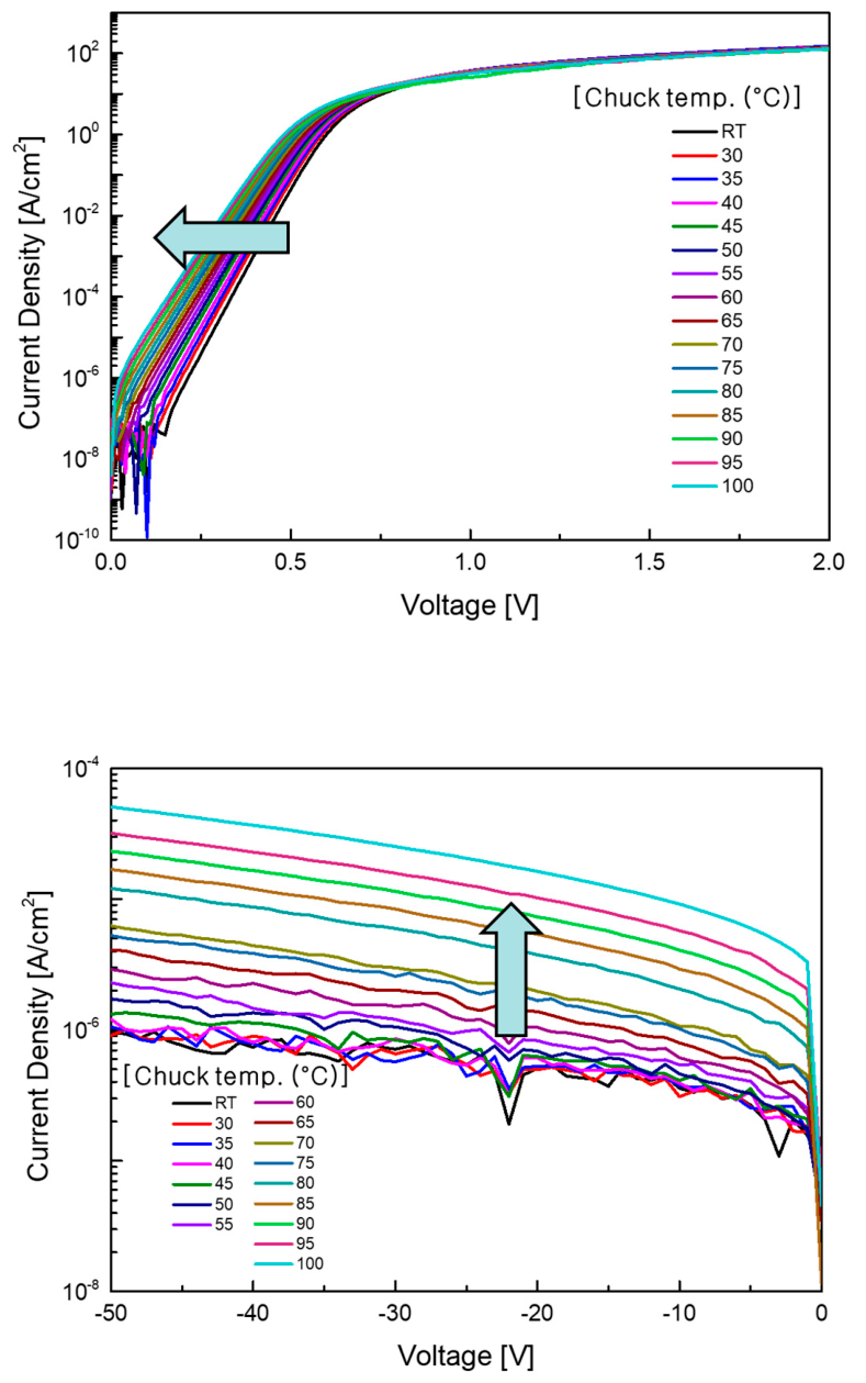
Figure 14.
Temperature-dependent I–V characteristics of Mo/β-Ga₂O₃ SBDs annealed at 550°C: (a) forward and (b) reverse bias.
Figure 14.
Temperature-dependent I–V characteristics of Mo/β-Ga₂O₃ SBDs annealed at 550°C: (a) forward and (b) reverse bias.
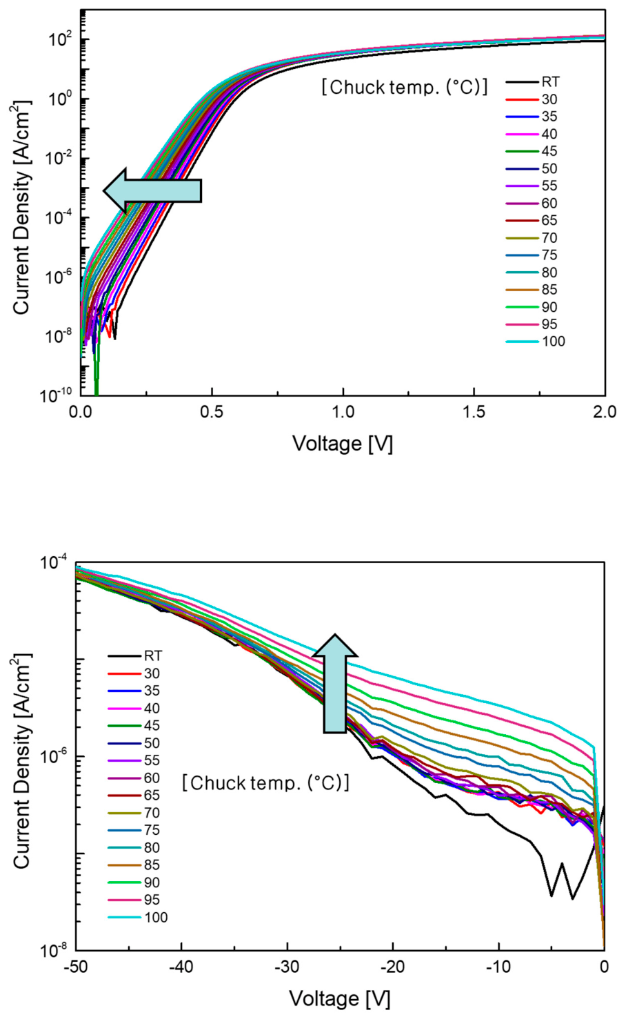
Table 3.
Parameters and fabrication conditions for Mo/β-Ga₂O₃ vertical SBDs.
| Material | Parameter | Value |
|---|---|---|
| Si doped Ga2O3 epi. | Nd-Na(cm-3) | 2.2 x 10¹⁶ |
| Sn doped Ga2O3 wafer | Nd-Na(cm-3) | 4.5 x 10¹⁸ |
| Back metal Ti / Au (ohmic contact) | Thickness | 10 / 40 nm |
| Base Pressure | 4 x10⁻⁶Torr | |
| Equipment | E-beam Evaporator | |
| Top metal Mo (Schottky contact) |
Thickness | 300nm |
| Base Pressure | 2 x 10⁻⁶Torr | |
| Working Pressure | 3mTorr | |
| Input Power | 30W | |
| Substrate Temperature | Room Temperature | |
| Active Area (mm2) | 0.07 | |
| Post Annealing Treatment | Post-annealing Temp. | 400°C, 500°C, 550°C |
| Working Gas, Working Pressure | Ar gas, 100 mTorr |
Disclaimer/Publisher’s Note: The statements, opinions and data contained in all publications are solely those of the individual author(s) and contributor(s) and not of MDPI and/or the editor(s). MDPI and/or the editor(s) disclaim responsibility for any injury to people or property resulting from any ideas, methods, instructions or products referred to in the content. |
© 2026 by the authors. Licensee MDPI, Basel, Switzerland. This article is an open access article distributed under the terms and conditions of the Creative Commons Attribution (CC BY) license (http://creativecommons.org/licenses/by/4.0/).
Copyright: This open access article is published under a Creative Commons CC BY 4.0 license, which permit the free download, distribution, and reuse, provided that the author and preprint are cited in any reuse.


