

Submitted:
18 July 2026
Posted:
20 July 2026
You are already at the latest version
Abstract
Short-wave infrared photodetector stacks based on Lead Sulphide (PbS) promise inexpensive and tunable responsivity in the infrared regime. However, the low charge carrier mobilities of PbS require additional electron (ETL) and hole transport (HTL) layers, which modifies the optical absorption Fabry-Perot profile within the two mirror-like electrodes. This creates a coupled design problem, where changes in transport layer thickness can redistribute optical energy away from the absorber or increase loss in the electrodes and transport layers, thus reducing useful absorption. Here, we introduce a cavity-partitioning perspective for planar PbS photodiode stack, treating the air/ITO/ETL/n-PbS/p-PbS/HTL/Au stack as a coupled lossy Fabry-Perot cavity whereby the electron and hole transport layer thicknesses control the partition of absorption between useful PbS photogeneration and parasitic loss. Subsequently, the HTL behaves as a phase tuning layer that can move the field antinode closer to the hole transport layer, while ETL behaves as a field strength control layer that modulates field amplitude near the electron transport layer.
Keywords:
lead sulphide
; SWIR photodiodes
; inverse design
; Fabry-Perot cavity
; parasitic absorption
1. Introduction
Short wave infrared photodetectors based on PbS colloidal quantum dots offer low temperature, solution processable detection with spectral tunability beyond the silicon band edge. Their bandgap can be controlled through nanocrystal size, enabling absorption across the short wave infrared range while retaining compatibility with thin film deposition and large area integration [1,2,3]. A key limitation, however, is charge transport. In PbS films, carriers move through charge hopping pathways [4,5,6] that significantly limit their mobility. Solution-processed PbS films typically exhibit mobilities from 10−6⁶-−20⁻2 −1m−1 V⁻¹ s⁻¹, with optimized low-temperature processed Field-Effect Transistors reaching 0.2-−1.−14 cm² V⁻¹ s⁻¹ [7,8,9]. By contrast, single crystal PbS can show room temperature Hall mobilities of seve2a−1 −1undred cm² V⁻¹ s⁻¹ [10,11,12], while silicon has electron and hole mobilities2o−1 −1500 and 450 cm² V⁻¹ s⁻¹ respectively [13]. This low mobility means that simply increasing the PbS absorber thickness to maximize absorbed optical power is not an efficient approach to higher photocurrent, because additional optical absorption can be offset by poorer carrier extraction [4]. The device operation thus requires electron and hole transport layers between the QD absorbing layers and the electrodes, which also become part of the optical cavity and modify the Fabry-Perot phase condition and can shift optical antinodes into parasitic regions [14,15].
Previous optical studies of quantum dot and thin film photodiodes have established that resonant cavity engineering can recover absorption in thin active layers without increasing the carrier collection length [16]. In PbS photodiodes, however, the cavity is not formed by the absorber and reflector alone. The ETL and HTL are electrically required to form high charge mobility contacts interfacing the quantum dot layers, yet their finite thicknesses and relatively high refractive indices make them active contributors to the optical phase. Figure 1a summarizes this objective space, where the desired design is one where the field maxima should lie inside the PbS region, with strong overlap across the electrically useful absorber volume, while field intensity in the surrounding contact and transport layers is suppressed [17,18]. Having multiple antinodes would increase the distribution of photoexcitation within the n-PbS/p-PbS region, which also adds another dimension to the optimization. This creates a coupled design problem in which a geometry that maximizes integrated PbS absorption may not distribute the standing wave field across the most electronically useful regions within the absorber. Conventional layer by layer sweeps identify favourable thickness combinations, but they do not directly distinguish whether a design improves absorption by increasing useful field overlap in PbS or by redistributing absorption through lossy transport and contact layers [19].
Conventional optical design for resonant PbS photodiodes therefore relies primarily on forward electromagnetic modeling, using transfer-matrix methods, RCWA or FDTD simulations, followed by manual tuning or parametric sweeps of selected layer thicknesses [20,21]. These approaches are useful because they expose how absorber, transport-layer and contact-layer thicknesses influence the cavity resonance, internal field distribution and absorption profile. Their limitation is that they normally examine only a small number of variables at a time, and the computational cost grows rapidly as additional layers or tolerance cases are included. They also tend to identify favorable thickness combinations or maximize total or active-layer absorption, rather than embedding the absorption partition between useful PbS absorption and parasitic loss in the contact, transport and reflector layers directly into the optimization target [14,22]. As a result, forward sweeps can reveal cavity behavior, but they are less efficient and less systematic for optimizing a coupled multilayer photodiode stack in which all layers contribute to the Fabry Perot phase condition and absorption distribution.
We thus approach this problem through a combination of Fabry Perot cavity interpretation, layer-resolved absorption partitioning and bounded adjoint inverse design in a single optimization framework for PbS SWIR photodiodes. Instead of maximizing total absorption by sweeping isolated layer thicknesses, the method jointly optimizes the multilayer cavity geometry to increase useful PbS absorption while penalizing parasitic absorption in the transport, contact and reflector layers. In this formulation, the contact, transport and reflector layers are treated not as passive electrical components surrounding the absorber, but as optical cavity elements that alter phase, field distribution and loss partitioning. The resulting design problem therefore searches for thickness combinations that preserve a favorable cavity condition while shifting the absorption partition toward the active absorption region.
In this work, we treat an air/ITO/ETL/n-PbS/p-PbS/HTL/Au stack as a lossy multilayer Fabry Perot cavity (Figure 1b), whereby ETL and HTLs are metal oxides with refractive index of 2.0 and 2.2 respectively. Full wave electromagnetic simulations are used to compute the field profile and layer resolved absorption at the target wavelength [23]. We first use forward thickness sweeps to identify the main optical roles of each layer, including field redistribution, absorption enhancement, and parasitic loss. This step reduces the design problem to the layer thicknesses that most strongly affect the cavity response. We then use bounded adjoint optimization to search this reduced design space [24,25,26]. In this workflow (Figure 1c), the sweeps define the initial design space, and the adjoint method searches it efficiently. All underlying data on the PbS material’s and other materials’ layer parameters were drawn from open-source literature [15].
This cavity argument can be written explicitly in terms of the various layers’ optical thickness. For layer , the optical-thickness contribution is
2. Methodology
Forward sweeps were used as a controlled way to map the cavity response before optimization. In each sweep, one or two layer thicknesses were varied over predefined bounds while the remaining stack parameters, source condition, boundary conditions and target wavelength were kept fixed. For each geometry, a full wave FDTD simulation was performed on the stack under normally incident illumination at 1.55 μm. The local loss density was calculated from the simulated electric field and complex permittivity, then integrated over selected layer regions to obtain absorbed power in the PbS active layers and in the non-PbS layers. One dimensional sweeps were used to isolate the roles of the contact and transport-side layers, while two-dimensional sweeps over PbS partitioning and PbS/transport-layer thickness were used to identify coupled cavity behaviour. These sweeps provided a physically interpretable map of how each layer thickness affects total PbS absorption, parasitic absorption and field distribution inside the absorber.
The adjoint optimization was carried out on the planar stack using four bounded thickness variables. These were the ITO thickness, front transport-layer thickness, total PbS thickness and back transport-layer thickness, while the Au reflector was fixed at 100 nm. The total PbS thickness was used as a single absorber variable and then divided into n-PbS and p-PbS using a fixed ratio of approximately 72.6 percent n-PbS and 27.4 percent p-PbS. Each unconstrained optimization variable was mapped to a physical thickness using , which kept all layers inside the allowed fabrication range during the optimization. At each iteration, a full wave FDTD simulation was run at the target wavelength and the local optical loss density was evaluated as . For the optimization objective, this loss density was laterally averaged to obtain , and layer masks were used to define layer integrated absorbed power proxies . This gave separate absorption terms for ITO, the front transport layer, n-PbS, p-PbS, the back transport layer and Au.
The loss function was defined to reward absorption in the PbS quantum dot layers while penalizing absorption in the metal contact and transport or contact layers. The useful absorption term was , the non metal parasitic term was , and the total absorbed power proxy was . Four scalar objective terms were then used. The PbS absorption improvement was , the absorption selectivity was , the Au penalty was , and the non metal parasitic penalty was . The minimized loss was , where the weights are , , and . The largest weight was placed on increasing PbS absorption, while selectivity and parasitic loss terms discouraged solutions where the gain in active layer absorption was accompanied by comparable absorption in the contact, transport-side or reflector layers. This form separates active-layer absorption from parasitic absorption in the same manner as layer-resolved absorption analyses of thin-film optoelectronic devices [17,18]. Relative to a conventional objective that would only maximize the useful absorber term , the cavity-aware formulation can be viewed as adding an absorption-partition contribution, , so that . This added contribution is required because the transport, contact and reflector layers participate in the optical cavity and can absorb optical power that does not generate useful photocurrent. The objective therefore favor design parameters that increase the absolute PbS absorption while also shifting the absorption partition toward the QD active region and away from transport, contact and reflector layers.
The optimization loop was implemented as a repeated sequence of thickness mapping, EM simulation, absorption post processing, gradient evaluation and parameter update. At iteration , the unconstrained parameter vector was first converted into the physical thickness vector , after which a Tidy3D model of the multilayer stack was constructed and simulated. The simulated fields and material permittivities were then passed to the absorption operator to evaluate the layer resolved terms entering . Because the loss is defined in terms of physical thicknesses while the optimizer updates the unconstrained variables, the gradient was transformed through the bounded mapping according to , or equivalently . The parameters were then updated using Adam as , which was used because the four thickness variables affect the cavity response with different sensitivities. During the run, the loss, gradient norm, layer thicknesses, PbS absorption, Au absorption, non metal parasitic absorption and absorption ratios were recorded at each iteration to connect numerical convergence with the redistribution of absorption across the stack.
3. Results and Discussion
The parametric sweeps’ goal is to determine the thickness ranges as optical design variable for the inverse design optimization. The transport-layer thicknesses are therefore swept separately to determine whether they mainly shift the cavity resonance or only change the absorption strength. Figure 2a shows that the transport-side layers have different sensitivities. When one transport-layer thickness is varied, the highest PbS volumetric absorption remains relatively unchanged at the same PbS thickness of 375nm. The lowest PbS absorption point changes in strength at lower (~180 nm) and higher thickness (~500nm), with a small shift in the PbS thickness. This response is therefore consistent with coupling and amplitude control. It changes how strongly the incident field couples into the cavity but it is not the dominant parameter for translating the resonance through the PbS region. The second transport-layer sweep gives a different result. Its thickness changes the PbS thickness at which the maximum absorption occurs, indicating that the round-trip optical phase is modified sufficiently to move the Fabry Perot condition. These observations show that the transport layers should be treated as coupled optical design variables rather than fixed electrical spacers.
Figure 2b determines whether the transparent front ITO contact can be used as a cavity tuning layer. Increasing ITO thickness from 10 nm to 100 nm produces only a small change in total absorbed power (Figure 2b-i), but it steadily reduces the PbS contribution and increases non-PbS absorption. The depth resolved absorption profiles of Figure 2b-ii show the reason. The main absorption lobes inside the PbS region remain broadly similar, but the thicker ITO case increases loss near the front side of the stack. This indicates that a thick ITO’s main effect is to reduce useful absorption by moving a larger fraction of optical dissipation into the front contact region. For optimization, this justifies keeping ITO thin and treating it mainly as a parasitic loss constraint rather than as an anti-node control parameter.
Figure 3 examines which thickness variables control the spatial distribution of absorption in the PbS region. In Figure 3a, the strongest PbS absorption follows diagonal bands that are nearly parallel to the constant total PbS thickness lines. The n-PbS and p-PbS layers therefore act mainly as a combined absorber for setting the cavity field distribution. The exact n-PbS to p-PbS split may still affect the local absorption profile within the active region, but the integrated PbS absorption is governed more strongly by the total PbS thickness.
Figure 3b-i and 3b-ii show how this total PbS thickness couples to a transport-side thickness. Strong PbS absorption is confined to narrow diagonal bands in the PbS and adjacent transport-layer thickness plane, indicating that field distribution depends on the combined optical path through the multilayer stack. The high absorption bands follow the white optical thickness iso lines more closely than the red physical thickness iso lines. A thinner layer can be optically equivalent with a thicker one if it lies along the middle of the resonance ridge. Thus, the optical thickness iso-lines show the dominant phase trend while the deviation between the ridge and the physical iso-line indicate the looseness of the multilayer cavity.
The white isolines clarify the compensation between PbS and the adjacent transport layer. A thicker adjacent transport layer generally requires a thinner PbS layer to keep the main absorption feature in a similar region inside the PbS absorber. Moving across the optical thickness iso lines changes the field placement and rapidly reduces PbS absorption. Moving along the same optical thickness direction better preserves the field-distribution condition while allowing the field profile within the absorber to be adjusted. This is analogous to spacer tuning in conventional thin film cavities, but here the spacer also plays an electrical transport role.
The comparison between Figure 3b-i and 3b-ii shows that changing the other transport-layer case from 10 nm to 100 nm changes the absorption magnitude but leaves the main diagonal band structure largely intact. The result therefore indicates that transport-side thicknesses mainly control coupling strength, field amplitude and the coupled optical path rather than acting as independent material-specific knobs. These results motivate a reduced design strategy in which total PbS thickness and transport-side thicknesses are used to preserve useful absorber field distribution and adjust absorption strength, while ITO is constrained to limit front contact loss.

Table 1.
The inverse design optimized results of the ITO electrode, front electron transport layer, PbS absorption region, and back hole transport layer.
Table 1.
The inverse design optimized results of the ITO electrode, front electron transport layer, PbS absorption region, and back hole transport layer.
| Optical Layer | Inverse design result |
|---|---|
| ITO thickness | 18.97 nm |
| Front electron transport layer thickness | 22.27 nm |
| Total PbS thickness | 359.72 nm |
| Back hole transport layer thickness | 45.10 nm |
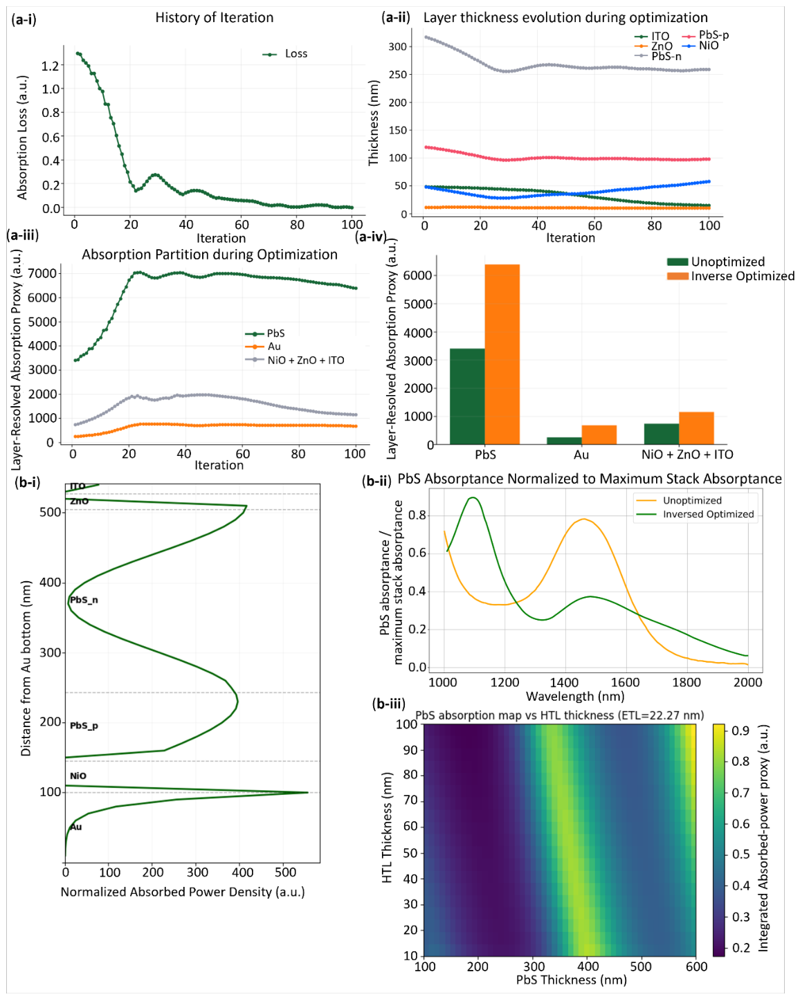
Figure 4a-i shows the behaviour of the bounded adjoint optimization. The loss decreases rapidly during the first 20 iterations and then enters a slower refinement stage. The early drop indicates that the optimizer quickly finds a thickness partition that improves the absorption objective. The smaller oscillations after this point are consistent with a cavity problem where small thickness changes can move the field maximum between neighbouring layers [27].
The thickness evolution in Figure 4a-ii shows how the optimizer satisfies the competing terms in the objective function. The largest change occurs in the PbS region. Both n-PbS and p-PbS become thinner, with the larger absolute change occurring in n-PbS because it occupies the larger share of the absorber. The ITO thickness also decreases, which is consistent with the objective because ITO absorption contributes to the parasitic loss term rather than to useful photocurrent generation. One transport-side variable remains close to its lower bound through most of the optimization, indicating that the optimizer does not require a large transport-layer thickness to meet the absorption objective. The other transport-side variable follows a different trend. It first decreases and then increases during the later iterations, showing that this thickness is used as a compensating variable to tune the cavity field while the absorber and transport-side thicknesses move toward values that improve the absorption partition. The absorption partition evolution in Figure 4a-iii confirms that the optimizer primarily increases useful PbS absorption. The PbS absorbed power rises strongly during the first 20 iterations. This increase is much larger than the increase in Au absorption or in the combined transport-side and ITO absorption. Au absorption increases and the combined transport and contact layer absorption also rise during the early iterations. After the first 20 iterations, the optimizer reduces the parasitic absorption to nearly its initial amount, with a small decrease in the PbS absorption. This reflects the practical trade-off in a lossy multilayer cavity. A stronger optical field in the stack improves PbS absorption, but some of that field also overlaps with lossy non active layers. Figure 4a-iv summarizes the net effect of the optimization. Relative to the initial unoptimized structure, the best optimized structure doubles the PbS absorbed power proxy. Au absorption and the combined transport-side and ITO absorption also increase, but by smaller absolute amounts. This outcome is consistent with the chosen objective. The optimizer favours a geometry where the gain in useful PbS absorption is large enough to justify a slight increase in parasitic loss.
The depth-resolved absorbed-power profile in Figure 4b-i shows that the optimized lossy-cavity concentrates the strongest absorption lobes inside the PbS active region while maintaining low absorption in the transport-side regions. The spectral response in Figure 4b-ii further shows a strong short-wavelength PbS absorption peak and a secondary response in the longer-wavelength SWIR region. Because the plotted PbS absorptance is normalized to a common maximum whole-stack absorptance, the comparison emphasizes how much of the available stack absorption is being associated with the PbS layer. The PbS thickness is slightly reduced relative to forward sweep baseline discussed in Figure 2, while the transport-side thicknesses are adjusted to preserve a favorable round-trip phase within the cavity. Figure 4b-iii confirms the optimization by mapping the PbS absorption as a function of total PbS thickness and a transport-side thickness at the optimized transport-layer setting. The middle of the ridge is likely where the resonance condition, PbS absorption volume, and parasitic loss balance most favourably. Along the absorption ridge, an intermediate transport-side thickness correlates with an intermediate PbS thickness, whereas an overly thick PbS layer or an overly thick transport-side layer is associated with poorer absorption partitioning within the active region. The balanced cavity solution therefore supports a generalized interpretation in which the transport-side layers adjust the phase condition and field distribution, while most of the absorption remains in the PbS active region.
4. Conclusion
This work shows that optical optimization of PbS quantum dot photodiodes is best treated as a coupled cavity design problem rather than as an absorber thickness problem. The forward sweeps show that total PbS thickness sets the main absorbing cavity condition, while the surrounding transport-side layers adjust the field distribution and absorption strength. ITO should remain thin because it increases non active absorption without improving the useful PbS contribution. The adjoint optimization then identifies a thickness partition that increases PbS absorption substantially while limiting, parasitic loss in the surrounding layers. The resulting design demonstrates that high performance requires both strong integrated absorption in the PbS layers and controlled redistribution of the optical field within the active region to improve charge-collection relevance, by considering the thin charge transport layers as optical design variables.
Funding
This work is partially supported by the 6th Royce Industrial Collaborative Program EP/X527257/1 and Royal Society Grant RGS\R2\242489.
Acknowledgments
The authors thank Rithichan Chhorn for simulation guidance.
Conflicts of Interest
The authors declare no conflict of interest.
References
- Zhao, X.; Ma, H.; Cai, H.; Wei, Z.; Bi, Y.; Tang, X.; Qin, T. Lead Chalcogenide Colloidal Quantum Dots for Infrared Photodetectors. Materials 2023, 16, 5790. [Google Scholar] [CrossRef] [PubMed]
- Konstantatos, G.; Sargent, E.H. Colloidal Quantum Dot Photodetectors. Infrared Phys. Technol. 2011, 54, 278–282. [Google Scholar] [CrossRef]
- Rogalski, A.; Kopytko, M.; Martyniuk, P.; Hu, W. Comparison of performance limits of the HOT HgCdTe photodiodes with colloidal quantum dot infrared detectors. Bull. Pol. Acad. Sci. Tech. Sci. 2020, 845–855. [Google Scholar] [CrossRef]
- Kagan, C.R.; Murray, C.B. Charge Transport in Strongly Coupled Quantum Dot Solids. Nat. Nanotech 2015, 10, 1013–1026. [Google Scholar] [CrossRef] [PubMed]
- Gao, Y.; Aerts, M.; Sandeep, C.S.S.; Talgorn, E.; Savenije, T.J.; Kinge, S.; Siebbeles, L.D.A.; Houtepen, A.J. Photoconductivity of PbSe Quantum-Dot Solids: Dependence on Ligand Anchor Group and Length. ACS Nano 2012, 6, 9606–9614. [Google Scholar] [CrossRef] [PubMed]
- Kim, D.; Kim, D.-H.; Lee, J.-H.; Grossman, J.C. Impact of Stoichiometry on the Electronic Structure of PbS Quantum Dots. Phys. Rev. Lett. 2013, 110, 196802. [Google Scholar] [CrossRef] [PubMed]
- Speirs, M.J.; Dirin, D.N.; Abdu-Aguye, M.; Balazs, D.M.; Kovalenko, M.V.; Loi, M.A. Temperature Dependent Behaviour of Lead Sulfide Quantum Dot Solar Cells and Films. Energy Environ. Sci. 2016, 9, 2916–2924. [Google Scholar] [CrossRef]
- Nugraha, M.I.; Yarali, E.; Firdaus, Y.; Lin, Y.; El-Labban, A.; Gedda, M.; Lidorikis, E.; Yengel, E.; Faber, H.; Anthopoulos, T.D. Rapid Photonic Processing of High-Electron-Mobility PbS Colloidal Quantum Dot Transistors. ACS Appl. Mater. Interfaces 2020, 12, 31591–31600. [Google Scholar] [CrossRef] [PubMed]
- Nugraha, M.I.; Kumagai, S.; Watanabe, S.; Sytnyk, M.; Heiss, W.; Loi, M.A.; Takeya, J. Enabling Ambipolar to Heavy N-Type Transport in PbS Quantum Dot Solids through Doping with Organic Molecules. ACS Appl. Mater. Interfaces 2017, 9, 18039–18045. [Google Scholar] [CrossRef] [PubMed]
- Balazs, D.M.; Matysiak, B.M.; Momand, J.; Shulga, A.G.; Ibáñez, M.; Kovalenko, M.V.; Kooi, B.J.; Loi, M.A. Electron Mobility of 24 Cm2 V−1 s−1 in PbSe Colloidal-Quantum-Dot Superlattices. Adv. Mater. 2018, 30, 1802265. [Google Scholar] [CrossRef] [PubMed]
- Pinna, J.; Pili, E.; Mehrabi Koushki, R.; Gavhane, D.S.; Carlà, F.; Kooi, B.J.; Portale, G.; Loi, M.A. PbI2 Passivation of Three Dimensional PbS Quantum Dot Superlattices Toward Optoelectronic Metamaterials. ACS Nano 2024, 18, 19124–19136. [Google Scholar] [CrossRef] [PubMed]
- Wang, L.; Wen, Y.; Tian, Y.; Zhu, Y.; Qin, B.; Gao, X.; Tan, Q.; Chang, C.; Zhao, L. High Carrier Mobility in N-Type PbS0.6 Se0.4 Crystal Enhances Thermoelectric Properties and Module Performance. Small 2025, 21, e08078. [Google Scholar] [CrossRef] [PubMed]
- Poncé, S.; Li, W.; Reichardt, S.; Giustino, F. First-Principles Calculations of Charge Carrier Mobility and Conductivity in Bulk Semiconductors and Two-Dimensional Materials. Rep. Prog. Phys. 2020, 83, 036501. [Google Scholar] [CrossRef] [PubMed]
- Georgitzikis, E.; Malinowski, P.E.; Maes, J.; Hadipour, A.; Hens, Z.; Heremans, P.; Cheyns, D. Optimization of Charge Carrier Extraction in Colloidal Quantum Dots Short-Wave Infrared Photodiodes through Optical Engineering. Adv. Funct. Mater. 2018, 28, 1804502. [Google Scholar] [CrossRef]
- Chehaibou, B.; Izquierdo, E.; Chu, A.; Abadie, C.; Cavallo, M.; Khalili, A.; Dang, T.H.; Gréboval, C.; Xu, X.Z.; Ithurria, S.; et al. The Complex Optical Index of PbS Nanocrystal Thin Films and Their Use for Short Wave Infrared Sensor Design. Nanoscale 2022, 14, 2711–2721. [Google Scholar] [CrossRef] [PubMed]
- Sulaman, M.; Yang, S.; Song, T.; Wang, H.; Wang, Y.; He, B.; Dong, M.; Tang, Y.; Song, Y.; Zou, B. High Performance Solution-Processed Infrared Photodiode Based on Ternary PbSx Se1−x Colloidal Quantum Dots. RSC Adv. 2016, 6, 87730–87737. [Google Scholar] [CrossRef]
- Burkhard, G.F.; Hoke, E.T.; McGehee, M.D. Accounting for Interference, Scattering, and Electrode Absorption to Make Accurate Internal Quantum Efficiency Measurements in Organic and Other Thin Solar Cells. Adv. Mater. 2010, 22, 3293–3297. [Google Scholar] [CrossRef] [PubMed]
- Pettersson, L.A.A.; Roman, L.S.; Inganäs, O. Modeling Photocurrent Action Spectra of Photovoltaic Devices Based on Organic Thin Films. J. Appl. Phys. 1999, 86, 487–496. [Google Scholar] [CrossRef]
- MacLeod, H.A.; Macleod, H.A. Thin-Film Optical Filters, 0 ed.; CRC Press, 2010; ISBN 978-0-429-13651-1. [Google Scholar]
- Katsidis, C.C.; Siapkas, D.I. General Transfer-Matrix Method for Optical Multilayer Systems with Coherent, Partially Coherent, and Incoherent Interference. Appl. Opt. 2002, 41, 3978. [Google Scholar] [CrossRef] [PubMed]
- Han, K.; Chang, C.-H. Numerical Modeling of Sub-Wavelength Anti-Reflective Structures for Solar Module Applications. Nanomaterials 2014, 4, 87–128. [Google Scholar] [CrossRef] [PubMed]
- Bae, S.; Duff, M.; Hong, J.Y.; Lee, J.-K. Optical Engineering of PbS Colloidal Quantum Dot Solar Cells via Fabry–Perot Resonance and Distributed Bragg Reflectors. Nano Converg. 2023, 10, 31. [Google Scholar] [CrossRef] [PubMed]
- Taflove, A.; Hagness, S.C. Computational Electrodynamics: The Finite-Difference Time-Domain Method. In Artech House antennas and propagation library, 3rd ed.; Artech House: Boston, 2005; ISBN 978-1-58053-832-9. [Google Scholar]
- Jensen, J.S.; Sigmund, O. Topology Optimization for Nano-photonics. Laser Amp Photonics Rev. 2011, 5, 308–321. [Google Scholar] [CrossRef]
- Molesky, S.; Lin, Z.; Piggott, A.Y.; Jin, W.; Vucković, J.; Rodriguez, A.W. Inverse Design in Nanophotonics. Nat. Photon 2018, 12, 659–670. [Google Scholar] [CrossRef]
- Yeung, C.; Ho, D.; Pham, B.; Fountaine, K.T.; Zhang, Z.; Levy, K.; Raman, A.P. Enhancing Adjoint Optimization-Based Photonic Inverse Design with Explainable Machine Learning. ACS Photonics 2022, 9, 1577–1585. [Google Scholar] [CrossRef]
- Xie, Z.; Jiang, J.; Jiang, F.; Chen, Y. Demonstrating the Antinode Loss Effect as the Operational Mechanism of Broadband Multilayer Film Absorbers. Opt. Express 2025, 33, 6734. [Google Scholar] [CrossRef] [PubMed]
Figure 1.
(a) Design parameter matrix. The axes are associated respectively with high absorber region volumetric absorption and spatial field distribution within the absorber. The upper quadrant represents an ideal scenario where most of the optical input is absorbed within the PbS layers but the optical field is retained within electronically useful absorber regions. (b) FDTD simulation region of the SWIR photodetector stack indicating the ITO and Au electrodes on both ends, the adjacent electron and hole transport layers, and the n-p PbS absorption region. (c) Inverse design optimization workflow. The initial design is mapped from unconstrained variables to bounded thicknesses, simulated and evaluated using layer-resolved absorption metrics. The objective functions are used by an Adam optimizer to update the design iteratively, while the loss, gradients, absorption values, and thickness evolutions are logged until convergence. .
Figure 1.
(a) Design parameter matrix. The axes are associated respectively with high absorber region volumetric absorption and spatial field distribution within the absorber. The upper quadrant represents an ideal scenario where most of the optical input is absorbed within the PbS layers but the optical field is retained within electronically useful absorber regions. (b) FDTD simulation region of the SWIR photodetector stack indicating the ITO and Au electrodes on both ends, the adjacent electron and hole transport layers, and the n-p PbS absorption region. (c) Inverse design optimization workflow. The initial design is mapped from unconstrained variables to bounded thicknesses, simulated and evaluated using layer-resolved absorption metrics. The objective functions are used by an Adam optimizer to update the design iteratively, while the loss, gradients, absorption values, and thickness evolutions are logged until convergence. .
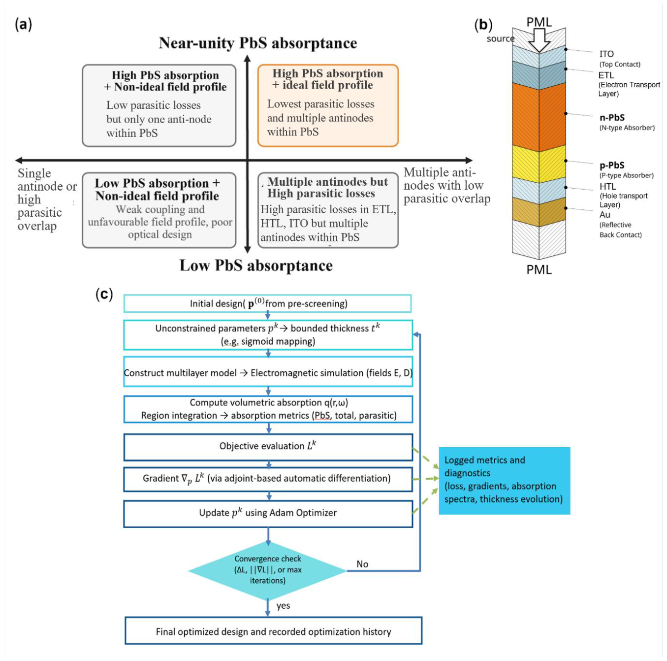
Figure 2.
Layer sensitivity and absorption partitioning in the PbS quantum dot photodiode cavity. (a-i) Forward sweeps of transport-layer thickness show that one layer mainly changes the absorption magnitude, while the main PbS absorption maximum remains near the same PbS thickness. (a-ii) A second transport-layer sweep shows a clearer shift of the absorption maximum, indicating that transport-layer phase effects can strongly modify the cavity field distribution. (b-i) Increasing ITO thickness reduces the PbS share of absorbed power and increases non PbS absorption, while total absorption changes only weakly. (b-ii) Depth resolved absorption profiles for 10 nm and 100 nm ITO show that thicker ITO increases front contact loss without substantially improving the absorber field profile. This shows that transport-side thicknesses modify the field distribution and absorption strength, while ITO should be kept thin to preserve absorption selectivity in the PbS layers.
Figure 2.
Layer sensitivity and absorption partitioning in the PbS quantum dot photodiode cavity. (a-i) Forward sweeps of transport-layer thickness show that one layer mainly changes the absorption magnitude, while the main PbS absorption maximum remains near the same PbS thickness. (a-ii) A second transport-layer sweep shows a clearer shift of the absorption maximum, indicating that transport-layer phase effects can strongly modify the cavity field distribution. (b-i) Increasing ITO thickness reduces the PbS share of absorbed power and increases non PbS absorption, while total absorption changes only weakly. (b-ii) Depth resolved absorption profiles for 10 nm and 100 nm ITO show that thicker ITO increases front contact loss without substantially improving the absorber field profile. This shows that transport-side thicknesses modify the field distribution and absorption strength, while ITO should be kept thin to preserve absorption selectivity in the PbS layers.
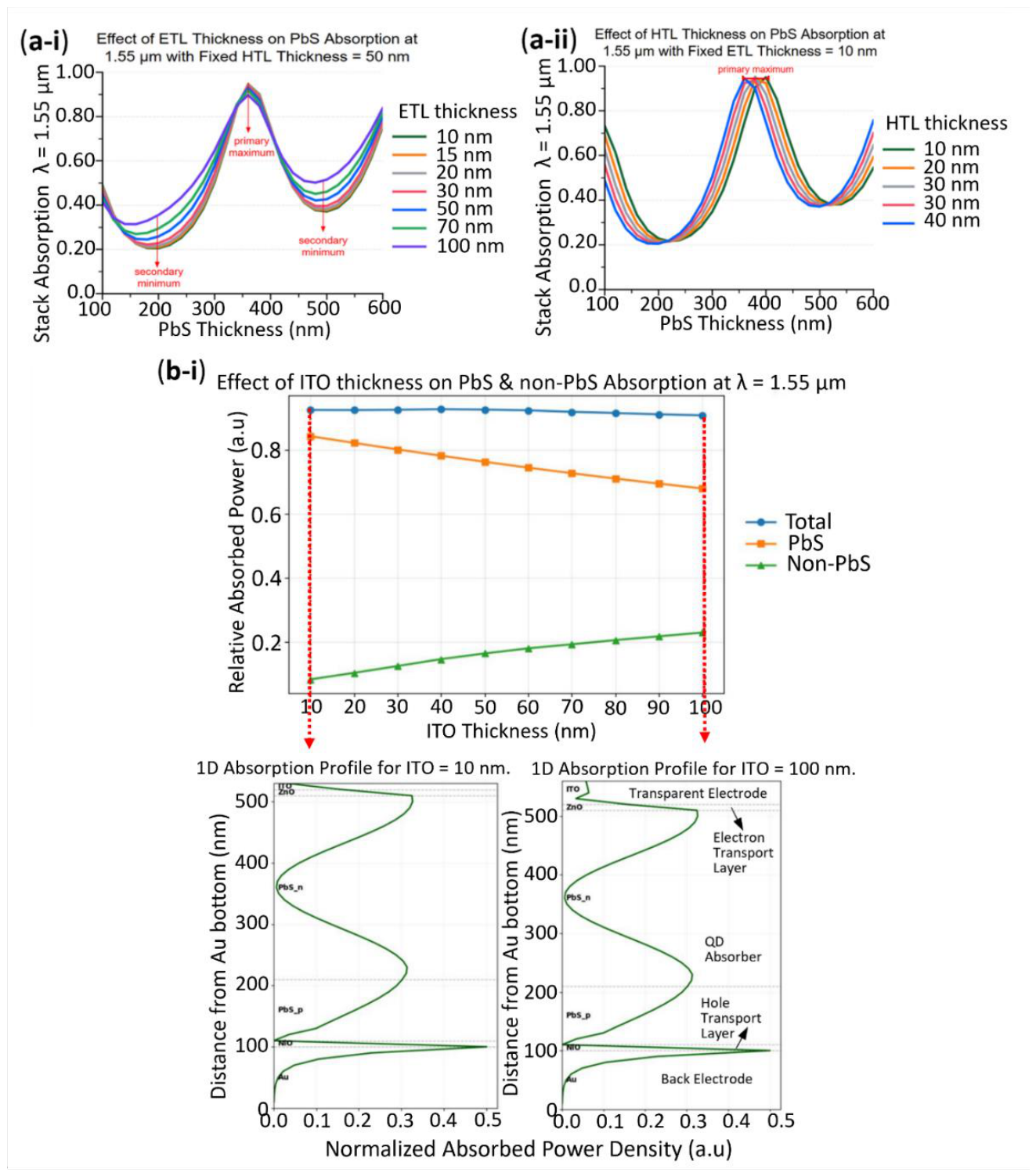
Figure 3.
Coupled PbS absorber and transport layer thickness dependence of the cavity absorption. (a) Layer resolved PbS absorbed power as a function of n-PbS and p-PbS thickness. The high absorption bands run nearly parallel to the constant total PbS thickness lines, showing that the integrated PbS response is governed mainly by the combined absorber thickness rather than the exact n-PbS to p-PbS partition. (b-i, -ii) PbS absorbed power as a function of total PbS thickness and adjacent transport-layer thickness for two transport-layer cases. Strong absorption is confined to narrow diagonal bands that follow the optical thickness iso lines more closely than the physical thickness iso lines.
Figure 3.
Coupled PbS absorber and transport layer thickness dependence of the cavity absorption. (a) Layer resolved PbS absorbed power as a function of n-PbS and p-PbS thickness. The high absorption bands run nearly parallel to the constant total PbS thickness lines, showing that the integrated PbS response is governed mainly by the combined absorber thickness rather than the exact n-PbS to p-PbS partition. (b-i, -ii) PbS absorbed power as a function of total PbS thickness and adjacent transport-layer thickness for two transport-layer cases. Strong absorption is confined to narrow diagonal bands that follow the optical thickness iso lines more closely than the physical thickness iso lines.
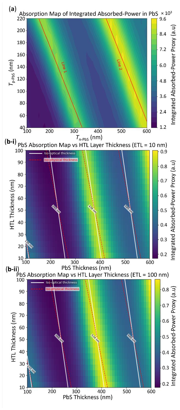
Figure 4.
Adjoint inverse design of the multilayer PbS quantum dot photodiode. (a-i) Loss history over 100 optimization iterations. The loss falls rapidly in the early iterations and then converges to a stable thickness partition. (a-ii) Evolution of the optimized layer thicknesses. The largest adjustment occurs in the PbS absorber, while the contact and transport-side layers remain relatively thin and provide additional tuning of the cavity field. (a-iii) Layer resolved absorption during optimization. PbS absorption increases strongly, while Au and combined transport-side and ITO absorption rise moderately. Later iterations reduce the non-metal parasitic contribution while maintaining high PbS absorption. (a-iv) Comparison of thicknesses between the initial unoptimized stack and optimized stack. The optimized design substantially increases the PbS absorbed power, with smaller accompanying increases in parasitic absorption. (b-i) The field profile within the cavity showing the absorption partition, whereby the strongest absorption is retained within the PbS region with small losses in the transport layers. (b-ii) The optical absorption spectrum shows the inversed optimized design have 80% of the stack absorption at the targeted 1550nm wavelength. (b-iii) The phase condition mapping of the PbS absorption at a optimized transport-layer setting.
Figure 4.
Adjoint inverse design of the multilayer PbS quantum dot photodiode. (a-i) Loss history over 100 optimization iterations. The loss falls rapidly in the early iterations and then converges to a stable thickness partition. (a-ii) Evolution of the optimized layer thicknesses. The largest adjustment occurs in the PbS absorber, while the contact and transport-side layers remain relatively thin and provide additional tuning of the cavity field. (a-iii) Layer resolved absorption during optimization. PbS absorption increases strongly, while Au and combined transport-side and ITO absorption rise moderately. Later iterations reduce the non-metal parasitic contribution while maintaining high PbS absorption. (a-iv) Comparison of thicknesses between the initial unoptimized stack and optimized stack. The optimized design substantially increases the PbS absorbed power, with smaller accompanying increases in parasitic absorption. (b-i) The field profile within the cavity showing the absorption partition, whereby the strongest absorption is retained within the PbS region with small losses in the transport layers. (b-ii) The optical absorption spectrum shows the inversed optimized design have 80% of the stack absorption at the targeted 1550nm wavelength. (b-iii) The phase condition mapping of the PbS absorption at a optimized transport-layer setting.
Disclaimer/Publisher’s Note: The statements, opinions and data contained in all publications are solely those of the individual author(s) and contributor(s) and not of MDPI and/or the editor(s). MDPI and/or the editor(s) disclaim responsibility for any injury to people or property resulting from any ideas, methods, instructions or products referred to in the content. |
© 2026 by the authors. Licensee MDPI, Basel, Switzerland. This article is an open access article distributed under the terms and conditions of the Creative Commons Attribution (CC BY) license (http://creativecommons.org/licenses/by/4.0/).
Copyright: This open access article is published under a Creative Commons CC BY 4.0 license, which permit the free download, distribution, and reuse, provided that the author and preprint are cited in any reuse.


