

Submitted:
14 July 2026
Posted:
15 July 2026
You are already at the latest version
Abstract
Wafer-edge uniformity in semiconductor etching is a key quality metric directly linked to device yield and is strongly governed by the local sheath structure near the wafer edge-focus ring boundary. However, the relative effects of focus ring geometry, dielectric material, and applied voltage waveform on edge ion transport have not been systematically compared. In this study, a two-dimensional particle-in-cell/Monte Carlo collision (PIC/MCC) simulation was performed for an argon capacitively coupled plasma to examine how focus ring height (15-26 mm), electrode-to-focus ring gap width (4-10 mm), dielectric permittivity (4.0 for quartz and 10.3 for Al2O3), and low frequency (LF) voltage affect plasma behavior and ion transport near the wafer edge. The voltage waveform effect was evaluated by comparing an HF-only single frequency (SF) condition, a baseline pulsed dual-frequency (Pulsed DF) condition with VLF=-1000 V and VHF=300 V, and an enhanced pulsed DF condition with VLF=-2000 V. Focus ring height and gap width were found to control edge ion incidence more directly than dielectric permittivity. A focus ring height matched to the powered electrode minimized sheath distortion and produced near-normal ion incidence, whereas a larger electrode-to-focus ring gap broadened the ion angular distribution. Increasing the relative permittivity from 4.0 to 10.3 modified the local electric field structure and reduced the outward ion flux near the focus ring but had only a modest effect on the overall plasma density. Under fixed focus ring geometry, increasing the LF voltage level strongly modified the wafer edge ion energy-angle distribution: the SF condition confined ions to a relatively narrow low-energy range near 200 eV, whereas the enhanced pulsed DF condition extended the ion energy to approximately 1400 eV. These results indicate that focus ring height and gap width are the primary design variables for controlling wafer edge ion incidence, while voltage waveform optimization is also required to control ion energy and improve wafer edge process uniformity.
Keywords:
plasma etching process
; capacitively coupled plasma
; focus ring design
; low-frequency voltage waveform
; ion energy-angle distribution (IEAD)
; wafer edge uniformity
; Particle-in-Cell/Monte Carlo Collision (PIC/MCC) simulation
1. Introduction
Plasma etching is a core unit process in semiconductor device manufacturing, governing critical dimension control, sidewall profile formation, and process yield. [1,2] As device architectures continue to transition toward three-dimensional structures such as 3D NAND and FinFET, and as feature dimensions approach atomic scales, maintaining etch uniformity across the entire wafer has become increasingly demanding [1,3]. In this context, uniformity at the wafer edge, a region historically excluded from the usable die area, has emerged as a critical factor directly linked to device yield and process efficiency, driving sustained research efforts toward reducing edge exclusion and improving edge-profile control [2,3,4,5]. The wafer edge presents a fundamentally different electrical environment from the wafer center. In capacitively coupled plasma (CCP) etching reactors, the height mismatch between the wafer and the surrounding electrode or focus ring structure causes the plasma sheath to bend near the wafer edge, distorting the ion energy and angular distribution and producing non-uniform etch profiles [5]. To compensate for this sheath deformation, a dielectric structure known as a focus ring is placed around the wafer edge. The focus ring modifies the local sheath geometry by changing the voltage division and electric field distribution near the wafer edge-focus ring boundary, thereby helping to guide ions toward more normal incidence at the wafer edge [6,7]. However, the structural parameters of the focus ring, including its height relative to the powered electrode, the gap between the wafer edge and the focus ring, and the dielectric permittivity of the focus ring material, strongly affect the local electric field distribution and sheath shape near the wafer edge [8,9,10] These changes can directly influence the ion energy-angle distribution (IEAD), which is a key determinant of edge-profile control [5,6,7,8,9]. The influence of focus ring structural parameters on ion transport at the wafer edge has been examined in several computational and experimental studies. Babaeva and Kushner developed a numerical model to investigate plasma penetration into the wafer-focus ring gap and ion energy and angular distributions near the wafer-focus ring structure [10,11]. They reported that the wafer-focus ring gap and focus ring geometry significantly modify ion incidence into the edge region and gap structure [10,11]. Kim et al. performed a quantitative two-dimensional PIC simulation study on the effects of focus ring geometry and permittivity on ion kinetics at the wafer edge in CCP reactors, examining gap size, focus ring height, and dielectric constant in a unified framework [8]. Ma et al. further investigated the effects of focus ring height, wafer-focus ring gap, and dielectric constant on ion kinetics at the wafer edge in CCP reactors [9]. Wang et al. investigated the effect of focus ring permittivity on the ion energy and angular distributions incident on the focus ring surface and on focus ring erosion rates, showing that higher permittivity increases the sheath voltage over the focus ring and intensifies erosion while reducing the incidence-angle skew at the wafer edge [4]. Xiao et al. developed a one-dimensional circuit model of a focus ring and validated it experimentally, demonstrating that the focus irng acts as part of the local voltage division at the wafer edge and that its geometry governs the wafer edge voltage distribution [6]. They subsequently extended this approach by incorporating a tunable external circuit to actively control the edge sheath dynamics over a wider range of operating conditions [7]. Seong et al. experimentally characterized how the height mismatch between the wafer and the electrode causes sheath bending and alters the etch profile, noting that while many simulation studies have addressed the focus ring-sheath relationship, corresponding experimental data remain limited [5]. In parallel, pulsed plasma operation has gained increasing attention as a strategy for improving etch uniformity and process control in CCP systems. In continuous-wave (CW) operation, gas dissociation and plasma density often increase together with applied power, making it difficult to independently control ion flux and the flux of reactive species. Pulsed plasma operation, in which the pulse-on and pulse-off durations can be adjusted, provides additional control over reactive species production, ion flux, and etch rate, and has been shown to improve etch selectivity and enable anisotropic etching in nanometer-scale processes [12,13]. In dual-frequency pulsed CCP systems, the low-frequency (LF) voltage component primarily controls ion acceleration by modulating the sheath voltage over the LF period [14,15], while the high-frequency component is more closely associated with plasma generation. Accordingly, the LF voltage can strongly affect the ion energy distribution function (IEDF), even when its contribution to plasma generation is limited [16]. Despite these advances, the combined influence of focus ring structural parameters and LF voltage on wafer edge ion transport in pulsed dual-frequency CCP systems has not been systematically examined. Prior studies have largely focused on the individual effects of focus ring geometry, focus ring erosion and lifetime, or bulk plasma uniformity controlled by the applied waveform. As a result, the relative importance of structural variables and voltage waveform conditions for wafer edge ion incidence remains insufficiently clarified.
In this work, a two-dimensional particle-in-cell/Monte Carlo collision (PIC/MCC) simulation of an argon CCP driven by pulsed RF waveforms is used to systematically examine how focus ring height, electrode-to-focus ring gap width, dielectric permittivity, and LF voltage affect plasma behavior and ion transport near the wafer edge [17,18]. Secondary electron emission from the wafer, powered electrode, grounded electrode, and focus ring surfaces is not considered in the present simulation, although surface-generated secondary electrons can influence argon discharge sustainment and sheath dynamics [19]. The time-averaged plasma potential, electric field, electron power absorption, electron density, ion flux, IEDF, and IEAD are analyzed for a range of focus ring configurations and driving conditions, including an HF-only single frequency (SF) condition, a baseline pulsed dual frequency condition, and an enhanced pulsed dual frequency condition. The interpretation of wafer edge ion bombardment is guided by established studies of RF sheath ion energy distributions plasma-processing ion kinetics, and waveform-controlled ion energy modulation in multi-frequency CCP systems [20,21,22,23,24,25,26,27,28,29,30].
2. Simulation Method
The simulations were performed using a two-dimensional, three-velocity-component Particle-in-Cell/Monte Carlo collision (2D3V PIC/MCC) code implemented in Cartesian coordinates on a GPU-accelerated platform [17,18]. Charged particles were advanced in the self-consistent electrostatic field calculated on a uniform Cartesian grid [17,18]. Electron-neutral and ion-neutral collisions, including elastic scattering, excitation, and ionization, were treated using the Monte Carlo collision procedure based on the null-collision method [18]. The main numerical and operating conditions, including a grid spacing of 0.2 mm, a time step of 10 ps, and an argon pressure of 20 mTorr, are summarized in Table 1.
The computational domain represents a cross-sectional model of a pulsed RF argon capacitively coupled plasma (CCP) reactor. The powered electrode was placed at the bottom boundary, with the silicon wafer and focus ring located on its upper surface, while the top boundary was assigned as the grounded electrode. The left boundary was treated as the axis of symmetry and was assigned a Neumann boundary condition. The focus ring was positioned next to the wafer edge on the powered-electrode side so that changes in the local sheath structure and edge ion incidence could be directly examined [8,9,10,11]. Secondary electron emission from the wafer, powered electrode, grounded electrode, and focus ring surfaces was not considered in the present simulation [21].
Three groups of focus ring cases were considered, as shown in Figure 1. First, the focus ring height, Lh, was varied as 15, 20, 22 and 26 mm, while the other geometric parameters were kept unchanged. This group was used to evaluate how the height difference between the focus ring and the powered-electrode surface affects sheath distortion near the wafer edge [8,9]. Second, the electrode-to-focus ring gap width, Lw, was varied as 4, 6, 8, and 10 mm at a fixed focus ring height. This group was used to examine the influence of lateral spacing between the wafer edge and the focus ring [10,11]. Third, the relative permittivity of the focus ring material was changed from 4.0, corresponding to quartz, to 10.3, corresponding to Al2O3. For the gap-width and permittivity cases, the focus ring height was fixed at 20 mm. This comparison was used to separate the material effect from the geometric effects [8,9]. The applied voltage waveforms are summarized in Figure 2. In the single frequency case, only the high frequency component was applied to the powered electrode as a sinusoidal voltage with an amplitude of 300 V and a frequency of 40 MHz the pulsed dual-frequency cases, a 400 kHz low frequency component was superimposed on the 40 MHz waveform, and the waveform was pulsed with a duty ratio of 0.3 [12,14,15,16]. Two LF voltage conditions were compared. In the baseline pulsed dual frequency case, the LF voltage was set to -1000 V. In the enhanced pulsed dual frequency case, the LF voltage was changed to -2000 V, while the HF voltage was kept at 300 V. Except for the parameter varied in each case group, the remaining simulation conditions were kept the same. After the discharge reached a periodic steady state, plasma diagnostics were collected over one complete LF cycle. The time-averaged plasma potential, electric field, electron power absorption, electron density, and ion flux distributions were obtained for each case. Ion energy-angle distributions were sampled at both the wafer center and the wafer edge to quantify how focus ring geometry and the applied voltage waveform affected ion bombardment conditions relevant to edge-profile control.
3. Results and Discussion
This section first examines the effects of focus ring geometry and material property on wafer-edge ion transport under the pulsed dual frequency condition. The focus ring height cases are analyzed to identify the height condition that minimizes sheath distortion and produces near-normal ion incidence. The electrode-to-focus ring gap and dielectric permittivity cases are then compared to determining whether geometric spacing or material property has a stronger influence on edge ion bombardment. Finally, the LF voltage effect is evaluated separately by comparing LF voltage levels of 0, -1000, and -2000 V under the same HF voltage condition. This sequence allows the dominant factors controlling wafer-edge ion incidence to be identified from a process-design perspective.
3.1. Effect of Focus Ring Height
Focus ring height is one of the primary geometric parameters that can modify the local sheath structure near the wafer edge. Since ion trajectories are largely determined by the sheath electric field, the plasma potential distribution was first examined to evaluate how the height mismatch between the wafer and the focus ring changes the edge sheath shape. Figure 3 shows the time-averaged plasma potential distributions for four focus ring height conditions. Figure 3(a-d) correspond to Lh=15, 20, 22 and 26 mm, respectively, while Figure 3(e-h) show the enlarged views of the wafer edge and focus ring region for each corresponding case. Equipotential lines are included in all panels to visualize the local sheath structure. As the focus ring height increases from 15 to 26 mm, the time-averaged plasma potential decreases noticeably. The maximum plasma potential decreases from 129.7 V at Lh=15 mm to 79.13 V at Lh =20 mm, and then to 66.31 V and 66.56 V at Lh =22 and 26 mm, respectively. The largest change occurs between Lh =15 and 20 mm, indicating that the potential structure is particularly sensitive to the transition from a lower focus ring to the heigh matched condition. In contrast, the difference between Lh =22 and 26 mm is small, suggesting that the plasma potential changes only weakly once the focus ring height exceeds the electrode level. The enlarged views in Figure 3(e-h) show that the local sheath structure near the wafer edge also changes with focus ring height. At Lh =15 mm, shown in Figure 3(e), the focus ring is lower than the wafer edge level, and the equipotential lines near the wafer-focus ring boundary exhibit an abrupt transition. This behavior reflects the geometric step between the wafer and the shorter focus ring. At Lh =20 mm, shown in Figure 3(f), the focus ring is aligned with the powered electrode surface, and the equipotential lines become smoother near the wafer edge. This indicates that local sheath distortion is reduced under the height-matched condition. At Lh =22 and 26 mm, shown in Figure 3(g, h), the focus ring protrudes above the electrode surface, and the equipotential lines bend more strongly around the focus ring top. This curvature indicates stronger local electric field distortion near the protruding focus ring edge. These changes in the plasma potential and local sheath shape are expected to affect the energy and angular characteristics of ions reaching the wafer center and wafer edge, as examined below through the IEAD analysis. Figure 4 shows the ion energy-angle distributions (IEADs) measured at the wafer center, Figure 4(a, c, e, g) and wafer edge Figure 4 (b, d, f, h), for focus ring heights of Lh =15, 20, 22 and 26 mm. The color scale is normalized to the maximum value of each distribution and plotted on a logarithmic scale to capture both the dominant ion population and weaker features. At the wafer center, all four cases in Figure 4(a, c, e, g) show similar IEAD structures. A high-energy population appears near 1000-1100 eV and is concentrated close to 0, while a lower-energy ion population appears near 200-250 eV. Both ion populations remain within a narrow angular range of approximately -. This indicates that ion incidence at the wafer center is only weakly affected by focus ring height because the center region is sufficiently far from the wafer edge/focus ring boundary. At the wafer edge, however, the IEAD changes noticeably with focus ring height. At Lh =15 mm (Figure 4(b)), where the focus ring is lower than the powered electrode surface, the high-energy population near 1000 eV becomes less concentrated, and the distribution spreads more broadly in both energy and angle. This suggests that the height mismatch between the wafer and the lower focus ring distorts the local ion trajectories near the edge, causing ions to deviate from normal incidence. At Lh=20 mm, shown in Figure 4(d), where the focus ring top surface is aligned with the wafer surface, the high-energy population near 1100 eV becomes sharply concentrated, and the angular distribution narrows toward 0. This indicates that the height-matched condition provides the most favorable ion incidence characteristics at the wafer edge, with ions arriving closest to the surface-normal direction. At Lh =22 mm, Figure 4(f), and Lh =26 mm, shown in Figure 4(h), the focus ring protrudes above the electrode surface. In these cases, the high-energy population remains near 1100 eV, but the angular distribution becomes slightly titled, indicating that an excessively high focus ring modifies the local sheath field and deflects ions away from the surface-normal direction. The lower-energy ion population near 200-250 eV also shows a slightly broader angular spread compared with the Lh =20 mm case. Overall, the matched-height condition of Lh =20 mm produces the most favorable wafer edge IEAD among the four focus ring heights examined. In this case, the ion angular distribution is the narrowest and the high-energy ion population is most clearly concentrated near normal incidence. In contrast, lowering or raising the focus ring away from the height-matched condition broadens the wafer edge IEAD and makes the ion incidence less favorable for anisotropic etching. Although the IEAD results indicate that the height-matched condition is favorable from the perspective of ion incidence angle, the effect of focus ring height on the electron density distribution should also be spatial process uniformity across the wafer and therefore provides additional information on how focus ring height affects wafer scale plasma behavior. The two-dimensional electron density distributions and the corresponding one-dimensional profiles along the wafer surface are shown in Figure 5(a-d) and Figure 5(e), respectively. The peak electron density varies with focus ring height. It is lowest at Lh = 15 mm, with a value of , increases to at both Lh= 20 and 22 mm, and reaches its highest value of at Lh= 26 mm. In all four cases, the two-dimensional maps show a qualitatively similar density distribution, with the peak density located in the central plasma region and a gradual decrease toward the wafer edge. The one-dimensional profiles in Figure 5(e) reveal a clear grouping behavior in the radial electron density distribution. At the wafer center, the Lh= 22 and 26 mm cases show similar electron densities, while the Lh= 15 and 20 mm cases form another group. The difference between these two groups is approximately 9.25 %. This grouping tendency remains in the bulk plasma region, where the same pairing is observed but the difference between the two groups increases to approximately 16.12 %. Near the wafer edge, the trend changes more distinctly. The Lh = 15 mm case shows a pronounced edge peak and gives the highest local electron density among the four cases, whereas the Lh = 20, 22, and 26 mm cases show similar electron densities near the edge. The difference between the Lh = 15 mm case and the other three cases near the wafer edge reaches approximately 39.39 %. This edge enhancement in the Lh = 15 mm case is likely associated with the strong inward directed electric field formed near the geometric step between the wafer and the lower focus ring surface. In contrast, when the focus ring height matches or exceeds the electrode surface, this step-induced local enhancement is reduced, resulting in a more monotonic decrease in electron density toward the wafer edge. To further examine the physical origin of these trends, Figure 6 shows enlarged distributions of the x-direction electric field, Ex, x-direction ion flux, and electron power absorption, , near the wafer edge and focus ring region for each focus ring height. At Lh= 15 mm, shown in Figure 6(a-c), a strong inward-directed electric field is concentrated near the step between the wafer edge and the lower focus ring surface. The x-direction ion flux is also enhanced near this region, and the electron power absorption is localized around the geometric discontinuity. This distorted local field structure is consistent with both the edge electron density peak observed in Figure 5(e) and the broad, less concentrated wafer-edge IEAD shown in Figure 4(b). At Lh= 20 mm, shown in Figure 6(d-f), the x-direction electric field near the wafer-focus ring boundary is significantly reduced. The inward ion flux near the wafer edge also decreases, and the electron power absorption becomes more spatially distributed along the electrode surface rather than being concentrated at a single geometric discontinuity. These features are consistent with the reduced sheath distortion and the narrowest wafer IEAD observed for this case. At Lh= 22 and 26 mm, shown in Figure 6(g-i) and Figure 6(j-l), respectively, the focus ring protrudes above the electrode surface. In these cases, the electric field develops a stronger outward-directed component near the upper inner edge of the protruding focus ring, and the ion flux pattern shifts from the wafer edge region toward this protruding edge. The electron power absorption also becomes increasingly localized near the upper inner edge of the protruding focus ring, with the strongest localization observed at Lh= 26 mm. This concentration of electric field and electron power absorption near the protruding focus ring edge helps explain the broader wafer edge IEAD and the distinct difference in edge electron density between the Lh= 15 mm case and the other height cases, as shown in Figure 4 and Figure 5.
3.2. Effect of Electrode-to-Focus Ring Gap
The preceding section showed that focus ring height strongly affects the local sheath shape and ion incidence characteristics at the wafer edge. The electrode-to-focus ring gap width, Lw, is another important geometric parameter because it determines the lateral spacing between the wafer edge and the focus ring. In this section, the focus ring height is fixed at the height-matched condition, Lh= 20 mm, and the effect of gap width is examined separately. Figure 7 shows the time-averaged plasma potential distributions for gap widths of Lw= 4, 6, 8, and 10 mm. The enlarged views of the wafer edge focus ring region are also shown with equipotential lines to visualize the local sheath structure. In contrast to the focus ring height cases discussed in Section 3.1, the plasma potential increases as the gap width increases. The maximum plasma potential increases from 79.03 V at Lw= 4 mm to 133.7 V at Lw= 6 mm, and then to 135.5 V and 136.5 V at Lw= 8 and 10 mm, respectively. The largest increase occurs between Lw= 4 and 6 mm, while the potential changes only weakly at larger gap widths.
This suggests that opening the gap from the narrowest condition strongly modifies the overall potential structure, whereas the response becomes weaker once the gap is further widened. The enlarged views in Figure 7 show that the local potential structure near the wafer-focus ring boundary changes markedly with gap width. At Lw= 4 mm, the smoothly between the wafer edge and the focus ring surface. This indicates that the local sheath is only weakly distorted under the narrow-gap condition. As Lw increases to 6 and 8 mm, the equipotential lines in the gap region become more curved and extend further above the electrode surface. As Lw = 10 mm, the potential curvature above the gap becomes most pronounced among the four cases. This growing curvature is expected to strengthen the lateral electric field component in the gap region, which can deflect ions away from normal incidence as they traverse the sheath near the wafer edge. Figure 8 shows the IEADs measured at the wafer center and wafer edge for each gap width. At the wafer center, all four cases show similar IEAD structures. A high-energy ion population appears near 1000-1100 eV, while a lower-energy ion population appears near approximately 200 eV. Both populations remain within a narrow angular range. This indicates that the ion incidence condition at the wafer center is largely unaffected by the gap-width variation because the center region is sufficiently far from the wafer edge/focus ring boundary. At the wafer edge, however, the IEAD responds sensitively to the electrode-to-focus ring gap width. At Lw=4 mm, the high-energy ion population near 1100 eV is sharply concentrated close to , indicating near-normal ion incidence at the wafer edge. This behavior is consistent with the compact and smooth potential structure observed in the gap region for this case. When the gap width increases to Lw= 6 mm, shown in Figure 8 (d), the high-energy population shifts slightly toward lower energy near 1000 eV, and the angular distribution begins to broaden beyond approximately . At Lw= 8 mm, shown in Figure 8(f), the angular broadening becomes more pronounced, and the high-energy population becomes less sharply defined. The relative contribution of the lower-energy ion population near 200 eV also increases. At Lw= 10 mm, shown in Figure 8(h), the wafer edge IEAD is the broadest among the four cases, with ions arriving over an angular range of approximately . The lower-energy ion contribution is also the largest in this case. These changes indicate that increasing the electrode-to-focus ring gap broadens the ion angular distribution and makes the ion incidence condition less favorable for anisotropic etching at the wafer edge. To further examine the physical origin of these trends, Figure 9 shows the time-averaged distributions of the x-direction electric field, Ex, x-direction ion flux, and electron power absorption, , near the wafer edge and focus ring region for each gap width. At Lw=4 mm, shown in Figure 9(a-c), the x-direction electric field in the gap region is relatively weak, and the inward ion flux near the wafer edge is limited. These features are consistent with the compact sheath structure and near-normal IEAD observed for this case. The electron power absorption is localized near the wafer edge corner, indicating that the local field distortion is confined to a relatively narrow region. As the gap width increases to Lw= 6 and 8 mm, the x-direction electric field in the gap region becomes stronger and extends over a wider region. The inward ion flux toward the wafer edge also increases, and the electron power absorption region expands laterally above the gap. This indicates that the disturbed sheath region becomes broader as the electrode-to-focus ring gap increases. At Lw=10 mm, the x-direction electric field in the gap region reaches the strongest magnitude among the four cases, and the inward ion flux near the wafer edge is also the largest. The electron power absorption forms a broad and intense region across the gap, indicating that the sheath above the gap is strongly perturbed under this condition. The plasma potential, IEAD, and local field/flux distributions therefore show a consistent trend. A narrow gap maintains a compact sheath structure and near-normal ion incidence at the wafer edge, whereas a wider gap enhances the lateral electric field component in the gap region and broadens the wafer edge IEAD. Within the examined gap width range, a smaller electrode-to-focus ring gap is therefore more favorable for maintaining a narrow ion angular distribution and reducing the contribution of lower-energy ions at the wafer edge. From a process-design perspective, this result suggests that the electrode-to-focus ring gap should be carefully minimized or controlled to improve edge-profile control in anisotropic plasma etching.
3.3. Effect of Focus Ring Permittivity
The results of Section 3.1 and Section 3.2 showed that the focus ring height and electrode-to-focus ring gap width are the dominant geometric parameters affecting wafer edge ion transport. In this section, the effect of the focus ring dielectric material is examined by comparing a quartz focus ring () with an Al2O3 focus ring (). The focus ring height and gap width are fluxed at Lh= 20 mm and Lw= 10 mm, respectively. Unlike the height and gap width variations, changing the relative permittivity does not modify the geometric boundary shape. Instead, it changes the dielectric response of the focus ring and can modify the local electric field distribution near the wafer edge-focus ring boundary through capacitive coupling at the dielectric surface. Therefore, the influence of permittivity is expected to appear mainly as a local redistribution of the plasma and field structure rather than as a large-scale modification of the discharge. Figure 10 shows the time-averaged electron density distributions for the two permittivity cases. The maximum electron density decreases slightly from for the quartz case to for the Al2O3 case, corresponding to a reduction of approximately 4.9 %. The one-dimensional profiles in Figure 10(c) show that the overall radial distribution of electron density is similar between the two cases, with a relatively flat central region and a gradual decrease toward the wafer edge. The maximum difference between the two profiles across the wafer surface is approximately 5.18 %, occurring near the bulk plasma region. These results indicate that increasing the focus ring permittivity from 4.0 to 10.3 has only a modest effect on the overall plasma density. However, the two-dimensional distributions show a noticeable local change near the wafer edge-focus ring region, suggesting that the dielectric material mainly affects the spatial redistribution of plasma near the dielectric boundary rather than the global discharge density. Figure 11 shows the time-averaged plasma potential distributions for the two permittivity cases, together with enlarged views of the wafer edge-focus ring region. The maximum plasma potential increases slightly from 79.18 V for the quartz case to 85.19 V for the Al2O3 case. Despite this increase, the local potential structure near the wafer edge-focus ring boundary changes only weakly, as shown in the enlarged views in Figure 11(b) and Figure 11(d). In both cases, the equipotential lines near the wafer edge transition smoothly, which is consistent with the height-matched focus ring condition. Compared with the quartz case, the Al2O3 case shows a slightly more compressed, equipotential-line distribution near the focus ring face. This difference indicates that the focus ring surface. This difference indicates that the higher-permittivity focus ring locally modifies the potential structure near the dielectric boundary but does not strongly distort the sheath shape near the wafer edge. Figure 12 shows the IEADs at the wafer center and wafer edge for both permittivity cases, together with the ion energy distribution functions (IEDFs) integrated over all angles at the wafer edge edge in Figure 12(e). At the wafer center, both cases show similar IEAD structure, with a higher-permittivity focus ring locally modifies the potential structure near the dielectric boundary but does not strongly distort the sheath shape near the wafer edge. Figure 12 shows the IEADs at the wafer center and wafer edge for both permittivity cases, together with the ion energy distribution functions (IEDFs) integrated over all angles at the wafer edge in Figure 12(e). At the wafer center, both cases show similar IEAD structures, with a high-energy ion population near 1100 eV and a lower-energy ion population near 200-230 eV. Both populations remain within a narrow angular range, confirming that the ion incidence conditions at the wafer center is insensitive to the change in focus ring permittivity. At the wafer edge, the two cases also show qualitatively similar IEAD structures. The high-energy ion population remains near 1100 eV, and the angular spread is limited to approximately in both cases. However, the Al2O3 case shows a slightly narrower angular distribution than the quartz case. In addition, the IEDF comparison in Figure 12(e) shows that the quartz case has a higher ion count at both the high-energy peak near 1100 eV and the lower-energy peak near 200 eV. This indicates that increasing the focus ring permittivity slightly reduces the ion flux reaching the wafer edge, while causing only a limited change in the ion energy and angular distributions. To clarify physical origin of these differences, Figure 13 shows the time-averaged distributions of the x-direction electric field, Ex, x-direction ion flux, and electron power absorption, , near the wafer edge-focus ring region for both permittivity cases. In the quartz case, shown in Figure 13(a-c), an inward-directed Ex-component is formed near the inner wall of the focus ring, and a corresponding inward ion flux is observed toward the wafer edge. The electron power absorption is concentrated near the wafer-electrode surface and shows a local enhancement near the inner corner of the focus ring. In the Al2O3 case, shown in Figure 13(d-f), the Ex-component near the focus ring inner wall is weaker than in the quartz case. This reduction is consistent with the higher dielectric permittivity modifying the capacitive coupling between the focus ring and the adjacent sheath, thereby reducing the local electric field strength near the focus ring surface. As a result, the inward ion flux toward the wafer edge is reduced, and the local electron power absorption near the focus ring inner corner becomes less intense. Overall, the focus ring permittivity affects the local electric field structure, electron density redistribution, and ion flux near the wafer edge-focus ring boundary. However, its influence on the wafer edge IEAD is weaker than that of the geometric parameters examined in Section 3.1 and Section 3.2. The main effect of increasing the permittivity is a local modification of the field and flux near the focus ring surface, rather than a fundamental change in the sheath geometry or bulk plasma density. From a process-design perspective, this suggests that focus ring permittivity can modify local edge conditions, whereas focus ring height and electrode-to-focus ring gap width remain the primary design variables for controlling wafer edge ion incidence.
3.4. Effect of LF Voltage on Wafer-Edge Plasma Structure
The previous sections examined the effects of focus ring height, electrode-to-focus ring gap, and dielectric permittivity on wafer edge ion transport under the baseline Pulsed DF condition with an LF voltage of -1000 V. In this section, the voltage waveform is varied while the focus ring geometry is fixed at Lh=20 mm and Lw=10 mm with quartz (). Three waveform conditions are compared: a single frequency (SF) condition without the LF component, the baseline Pulsed DF condition (LF=-1000 V), and an enhanced Pulsed DF condition (LF=-2000 V). In dual frequency CCP systems, the LF component mainly modulates the sheath voltage over the LF period and therefore affects ion acceleration, whereas the HF component is more closely related to plasma generation [14,22]. Therefore, changing the LF voltage is expected to affect not only the ion energy distribution but also the sheath shape and the local ion transport near the wafer edge. Figure 14 show the time-averaged electron density distributions for the SF and enhanced Pulsed DF conditions, together with the one-dimensional density profiles along the wafer surface for all three waveform conditions. The peak electron density decreases from in the SF case to in the enhanced Pulsed DF case, corresponding to a reduction of approximately 36 %. This result indicates that the addition and strengthening of the LF component do not simply increase the plasma density, even though they strongly modify the sheath voltage. Under the SF condition, the discharge is sustained only by the HF voltage, and the density distribution remains more compact than in the enhanced Pulsed DF case. The one-dimensional profile in Figure 14(c) further shows that the SF case has a distinct edge peak near . At this location, the electron density is approximately 110.16 % higher than that in the baseline Pulsed DF case. This edge peak does not appear in either Pulsed DF case, where the radial density profiles are comparatively flat. The localized density enhancement in the SF case is likely related to HF-driven ionization near the wafer-focus ring boundary, where the corner geometry can concentrate the electric field when LF sheath modulation is absent. By contrast, the difference between the two Pulsed DF cases is much smaller: approximately 12.30 % at the wafer center and 9.69 % in the intermediate region. Thus, increasing the LF voltage from -1000 V to -2000 V changes the bulk density only moderately compared with the much larger change caused by removing the LF component. Figure 15 shows the time-averaged plasma potential distributions for the SF and enhanced Pulsed DF conditions. The peak plasma potential increases from 100.5 V in the SF case to 138.2 V in the enhanced Pulsed DF case. This increase is consistent with the stronger sheath modulation produced by the larger LF voltage in the Pulsed DF discharge. The enlarged views in Figure 15(b) and Figure 15 (d) show that the local sheath structure near the wafer edge is also clearly different between the two cases. In the SF case, the equipotential lines are closely spaced near the electrode surface, indicating that most of the potential drop occurs over a relatively narrow sheath region. In the enhanced Pulsed DF case, the equipotential lines extend farther above the electrode and bend over the gap between the wafer edge and the focus ring. This wider and more curved potential structure indicates that the LF-driven sheath expansion increases the spatial extent of the sheath field. As a result, the lateral electric field component near the gap becomes more extended, which directly affects the direction and spatial distribution of ions transported toward the wafer edge. Figure 16 shows the time-averaged distributions of the x-direction electric field Ex, x-direction ion flux, and electron power absorption near the wafer edge for the SF condition (Figure 16(a-c)) and the enhanced Pulsed DF condition (Figure 16(d-f)). In the SF case, Ex is concentrated near the inner corner of the focus ring (Figure 16(a)). Although the local field intensity is high, the field region is narrow. The inward ion flux in Figure 16(b) follows this localized field structure and is mainly directed toward the wafer edge corner. The electron power absorption in Figure 16(c) is also concentrated near the electrode surface adjacent to the focus ring. This behavior is consistent with the compact sheath structure observed in Figure 15: without LF modulation, the sheath field is confined close to the electrode, and the lateral field responsible for ion deflection is limited to a narrow region. In the enhanced Pulsed DF case, the distributions are broader. The x-direction electric field extends over a larger region above the gap and shows a clear inward component from the electrode surface to a position above the wafer level (Figure 16(d)). The inward ion flux is also larger and more widely distributed than in the SF case (Figure 16(e)), indicating that ions are redirected toward the wafer edge over a broader part of the sheath. The electron power absorption in Figure 16(f) spreads across the electrode surface and into the adjacent plasma region. This broader heating region suggests that the stronger LF sheath modulation changes the electron dynamics as well as the ion transport pathway. Therefore, the LF voltage does not only control the ion energy through sheath voltage modulation; it also changes where the electric field, ion flux, and electron heating are distributed near the wafer edge. These results show that the LF voltage strongly affects wafer edge plasma behavior under fixed focus ring geometry. Removing the LF component leads to a higher electron density, a clear density peak near the wafer edge, a compact sheath, and a narrow inward ion flux concentrated near the wafer-edge corner. Increasing the LF voltage to -2000 V produces a more extended sheath, a broader lateral electric field, and a wider inward ion flux distribution near the wafer edge. Therefore, the LF voltage can be used as an additional control parameter for adjusting wafer edge ion transport, together with the focus ring geometry parameters discussed in Section 3.1, Section 3.2 and Section 3.3.
4. Conclusions
In this study, a two-dimensional PIC/MCC simulation of a pulsed RF argon CCP was used to systematically examine how focus ring height, electrode-to-focus ring gap, dielectric permittivity, and LF voltage affect plasma behavior and ion transport near the wafer edge. The time-averaged plasma potential, electric field, electron density, ion flux, and electron power absorption were analyzed for a range of focus ring configurations and driving conditions, and the following conclusions were drawn. Among the focus ring structural parameters, the focus ring height had the most direct influence on wafer edge ion incidence. When the focus ring height was matched to the powered electrode level Lw=20 mm, edge sheath distortion was minimized and ions arrived at the wafer surface with near-normal incidence. Deviations from this matched-height condition altered the local sheath shape and degraded ion directionality. The peak plasma potential decreased from 129.7 V at Lh=15 mm to approximately 66 V at Lh=22-26 mm, and the radial electron density non-uniformity increased with focus ring height. Increasing the electrode-to-focus ring gap from 4 to 10 mm intensified the local electric field distortion above the gap region, broadened the ion angular distribution, and increased the low energy ion fraction at the wafer edge. The peak plasma potential also increased from 79.0 V to 136.5 V as the gap widened, which is consistent with stronger sheath distortion near the wafer-edge and focus ring boundary. These results indicate that a narrower gap is preferable for suppressing lateral field distortion and controlling the ion incidence angle at the wafer edge. Increasing the focus ring permittivity from 4.0, corresponding to quartz, to 10.3, corresponding to Al2O3, reduced the outward ion flux near the focus ring surface and produced a modest increase in plasma potential from 79.2 V to 85.2 V. However, the effect on bulk electron density was small, with a difference of approximately 5.2 %, and the radial uniformity and electron power absorption were largely unchanged. Therefore, dielectric permittivity acts as a secondary design variable compared with focus ring height and electrode-to-focus ring gap. The LF voltage also modified the plasma structure and ion transport at the wafer edge under fixed focus ring geometry. Removing the LF component, corresponding to the SF condition, produced a higher electron density with a pronounced edge peak and a spatially localized sheath, resulting in a narrow and concentrated inward ion flux near the wafer- edge corner. In contrast, increasing the LF voltage to -2000 V produced a wider and more curved sheath, a stronger lateral electric field, and a broader spatial distribution of inward ion flux at the wafer edge. Overall, the present results show that wafer edge ion transport in pulsed CCP etching is governed by the coupled effects of focus ring geometry and voltage waveform. Among the investigated structural showed stronger influence on sheath deformation and ion incidence direction than dielectric permittivity. The LF voltage condition further modified the spatial extent of the sheath, the lateral electric field near the wafer edge, and the inward ion flux distribution, even when the focus ring geometry was fixed. These findings suggest that accurate control of wafer edge ion incidence requires simultaneous consideration of both the local focus ring structure and the applied RF waveform, rather than optimization of either factor alone.
Author Contributions
Conceptualization, S.J.H. and H.J.L.; methodology, S.J.H.; software, S.J.H.; validation, S.J.H. and H.J.L.; formal analysis, S.J.H.; investigation, S.J.H.; resources, H.J.L.; data curation, S.J.H.; writing—original draft preparation, S.J.H.; writing—review and editing, S.J.H. and H.J.L.; visualization, S.J.H.; supervision, H.J.L.; project administration, H.J.L.; funding acquisition, H.J.L. All authors have read and agreed to the published version of the manuscript.
Funding
This research was funded by the 2024 BK21 FOUR Graduate School Innovation Support funded by Pusan National University (PNU-Fellowship program).
Data Availability Statement
The original contributions presented in this study are included in the article. Further inquiries can be directed to the corresponding author.
Conflicts of Interest
The authors declare no conflicts of interest. The funders had no role in the design of the study; in the collection, analyses, or interpretation of data; in the writing of the manuscript; or in the decision to publish the results.
Abbreviations
The following abbreviations are used in this manuscript:
| CCP | Capacitively coupled plasma |
| PIC | Particle-in-cell |
| MCC | Monte Carlo collision |
| IEADs | Ion energy-angle distributions |
| IEDF | Ion energy distribution function |
| RF | Radio frequency |
| HF | High frequency |
| LF | Low frequency |
| SF | Single frequency |
| DF | Dual frequency |
| FR | Focus ring |
| GPU | Graphics processing unit |
| DC | Direct current |
| CW | Continuous wave |
References
- Oehrlein, G.S.; Brandstadter, S.M.; Bruce, R.L.; Chang, J.P.; DeMott, J.C.; Donnelly, V.M.; Dussart, R.; Fischer, A.; Gottscho, R.A.; Hamaguchi, S.; Honda, M.; Hori, M.; Ishikawa, K.; Jaloviar, S.G.; Kanarik, K.J.; Karahashi, K.; Ko, A.; Kothari, H.; Kuboi, N.; Kushner, M.J.; Lill, T.; Luan, P.; Mesbah, A.; Miller, E.; Nath, S.; Ohya, Y.; Omura, M.; Park, C.; Poulose, J.; Rauf, S.; Sekine, M.; Smith, T.G.; Stafford, N.; Standaert, T.; Ventzek, P.L.G. Future of plasma etching for microelectronics: Challenges and opportunities. J. Vac. Sci. Technol. B 2024, 42, 041501. [Google Scholar] [CrossRef]
- Donnelly, V.M.; Kornblit, A. Plasma etching: Yesterday, today, and tomorrow. J. Vac. Sci. Technol. A 2013, 31, 050825. [Google Scholar] [CrossRef]
- Huang, S.; Huard, C.; Shim, S.; Nam, S.K.; Song, I.-C.; Lu, S.; Kushner, M.J. Plasma etching of high aspect ratio features in SiO2 using Ar/C4F8/O2 mixtures: A computational investigation. J. Vac. Sci. Technol. A 2019, 37, 031304. [Google Scholar] [CrossRef]
- Wang, X.; Lee, H.; Nam, S.K.; Kushner, M.J. Erosion of focus rings in capacitively coupled plasma etching reactors. J. Vac. Sci. Technol. A 2021, 39, 063002. [Google Scholar] [CrossRef]
- Seong, I.; Lee, J.; Kim, S.; Lee, Y.; Cho, C.; Lee, J.; Jeong, W.; You, Y.; You, S. Characterization of an etch profile at a wafer edge in capacitively coupled plasma. Nanomaterials 2022, 12, 3963. [Google Scholar] [CrossRef] [PubMed]
- Xiao, Y.; Du, Y.; Smith, C.; Nam, S.K.; Lee, H.; Lee, J.-Y.; Shannon, S. Focus ring geometry influence on wafer edge voltage distribution for plasma processes. J. Vac. Sci. Technol. A 2021, 39, 043006. [Google Scholar] [CrossRef]
- Xiao, Y.; Du, Y.; Smith, C.; Nam, S.K.; Lee, H.; Lee, J.-Y.; Shannon, S. Effect of focus ring with external circuit on cathode edge sheath dynamics in a capacitively coupled plasma. J. Vac. Sci. Technol. A 2023, 41, 033008. [Google Scholar] [CrossRef]
- Kim, J.S.; Hur, M.Y.; Kim, H.J.; Lee, H.J. The ion kinetics at the wafer edge by the variation of geometry and permittivity of the focus ring in capacitively coupled discharges. J. Appl. Phys. 2019, 126, 233301. [Google Scholar] [CrossRef]
- Ma, F.-F.; Zhang, Q.-Z.; Han, D.-M.; Xiong, Z.-L.; Wang, Y.-N. Effects of the focus ring on the ion kinetics at the wafer edge in capacitively coupled plasma reactors. J. Vac. Sci. Technol. A 2023, 41, 043002. [Google Scholar] [CrossRef]
- Babaeva, N.Y.; Kushner, M.J. Penetration of plasma into the wafer-focus ring gap in capacitively coupled plasmas. J. Appl. Phys. 2007, 101, 113307. [Google Scholar] [CrossRef]
- Babaeva, N.Y.; Kushner, M.J. Ion energy and angular distributions into the wafer-focus ring gap in capacitively coupled discharges. J. Phys. D Appl. Phys. 2008, 41, 062004. [Google Scholar] [CrossRef]
- Economou, D.J. Pulsed plasma etching for semiconductor manufacturing. J. Phys. D Appl. Phys. 2014, 47, 303001. [Google Scholar] [CrossRef]
- Kim, H.J.; Yeom, G.Y. Asynchronously pulsed plasma for high aspect ratio nanoscale Si trench etch process. ACS Appl. Nano Mater. 2023, 6, 10097–10105. [Google Scholar] [CrossRef]
- Boyle, P.C.; Ellingboe, A.R.; Turner, M.M. Independent control of ion current and ion impact energy onto electrodes in dual frequency plasma devices. J. Phys. D Appl. Phys. 2004, 37, 697–701. [Google Scholar] [CrossRef]
- Zhang, Y.; Kushner, M.J.; Sriraman, S.; Marakhtanov, A.; Holland, J.; Paterson, A. Control of ion energy and angular distributions in dual-frequency capacitively coupled plasmas through power ratios and phase: Consequences on etch profiles. J. Vac. Sci. Technol. A 2015, 33, 031302. [Google Scholar] [CrossRef]
- Rauf, S.; Tian, P.; Kenney, J.; Dorf, L. Effect of low frequency voltage waveform on plasma uniformity in a dual-frequency capacitively coupled plasma. J. Vac. Sci. Technol. B 2022, 40, 032202. [Google Scholar] [CrossRef]
- Hur, M.Y.; Kim, J.S.; Song, I.C.; Verboncoeur, J.P.; Lee, H.J. Model description of a two-dimensional electrostatic particle-in-cell simulation parallelized with a graphics processing unit for plasma discharges. Plasma Res. Express 2019, 1, 015016. [Google Scholar] [CrossRef]
- Shin, J.H.; Kim, H.; Lee, H.J. Two-dimensional particle-in-cell simulation parallelized with graphics processing units for the investigation of plasma kinetics in a dual-frequency capacitively coupled plasma. Rev. Mod. Plasma Phys. 2022, 6, 30. [Google Scholar] [CrossRef]
- Phelps, A.V.; Petrovic, Z.L. Cold-cathode discharges and breakdown in argon: Surface and gas phase production of secondary electrons. Plasma Sources Sci. Technol. 1999, 8, R21–R44. [Google Scholar] [CrossRef]
- Kawamura, E.; Vahedi, V.; Lieberman, M.A.; Birdsall, C.K. Ion energy distributions in rf sheaths; review, analysis and simulation. Plasma Sources Sci. Technol. 1999, 8, R45–R64. [Google Scholar] [CrossRef]
- Lieberman, M.A.; Lichtenberg, A.J. Principles of Plasma Discharges and Materials Processing, 2nd ed.; Wiley: Hoboken, NJ, USA, 2005; pp. 1–757. [Google Scholar]
- Wang, S.B.; Wendt, A.E. Control of ion energy distribution at substrates during plasma processing. J. Appl. Phys. 2000, 88, 643–646. [Google Scholar] [CrossRef]
- Economou, D.J. Tailored ion energy distributions on plasma electrodes. J. Vac. Sci. Technol. A 2013, 31, 050823. [Google Scholar] [CrossRef]
- Turner, M.M.; Derzsi, A.; Donkó, Z.; Eremin, D.; Kelly, S.J.; Lafleur, T.; Mussenbrock, T. Simulation benchmarks for low-pressure plasmas: Capacitive discharges. Phys. Plasmas 2013, 20, 013507. [Google Scholar] [CrossRef]
- Schulze, J.; Donkó, Z.; Luggenhölscher, D.; Czarnetzki, U. Different modes of electron heating in dual-frequency capacitively coupled radio frequency discharges. Plasma Sources Sci. Technol. 2009, 18, 034011. [Google Scholar] [CrossRef]
- Lafleur, T. Tailored-waveform excitation of capacitively coupled plasmas and the electrical asymmetry effect. Plasma Sources Sci. Technol. 2016, 25, 013001. [Google Scholar] [CrossRef]
- Kim, C.H.; Kim, H.; Park, G.; Shin, J.H.; Lee, H.J. Two-dimensional analysis for the transition from nonlocal to local electron kinetics and its effect on the spatial uniformity of a capacitively coupled plasma. Plasma Processes Polym. 2022, 19, e2100196. [Google Scholar] [CrossRef]
- Kim, C.H.; Kim, J.S.; Hur, M.Y.; Sakiyama, Y.; Lee, H.J. Transition of electron kinetics and its effect on ion energy and angular distributions at the boundary in intermediate-pressure capacitively coupled plasmas. Plasma Sources Sci. Technol. 2021, 30, 075005. [Google Scholar] [CrossRef]
- Zhang, Y.; Zafar, A.; Coumou, D.J.; Shannon, S.C.; Kushner, M.J. Control of ion energy distributions using phase shifting in multi-frequency capacitively coupled plasmas. J. Appl. Phys. 2015, 117, 233302. [Google Scholar] [CrossRef]
- Rauf, S.; Schroeder, M.; Korolov, I.; Kenney, J.; Schulze, J. Plasma dynamics in a capacitively coupled discharge driven by a combination of a single high frequency and a tailored low frequency rectangular voltage waveform. Plasma Sources Sci. Technol. 2023, 32, 034002. [Google Scholar] [CrossRef]
Figure 1.
Schematic of the two-dimensional simulation domain used in this study. (a) Variation of the focus ring height, Lh, at fixed gap with and dielectric permittivity. (b) Variation of the electrode-to-focus ring gap width, Lw, at fixed focus ring height and dielectric permittivity. (c) Variation of the focus ring dielectric permittivity at fixed height and gap width; cyan indicates Al2O3 (, while yellow indicates quartz ().
Figure 1.
Schematic of the two-dimensional simulation domain used in this study. (a) Variation of the focus ring height, Lh, at fixed gap with and dielectric permittivity. (b) Variation of the electrode-to-focus ring gap width, Lw, at fixed focus ring height and dielectric permittivity. (c) Variation of the focus ring dielectric permittivity at fixed height and gap width; cyan indicates Al2O3 (, while yellow indicates quartz ().
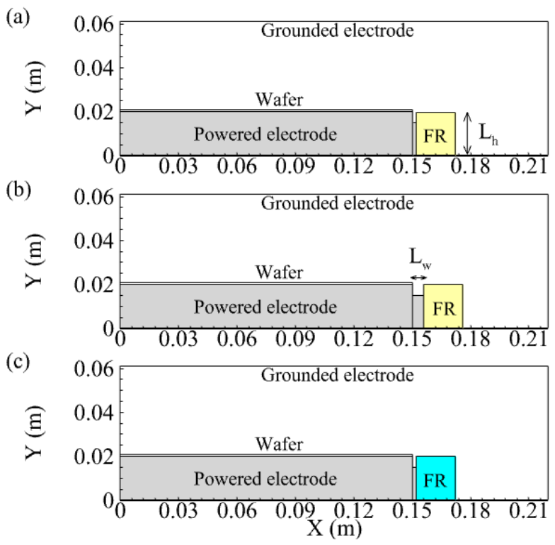
Figure 2.
Applied voltage waveforms used in this study. (a) Single frequency (SF) condition: HF sinusoidal waveform with an amplitude of 300 V and a frequency of 40 MHz, shown over one HF cycle. (b) Baseline pulsed dual frequency (Pulsed DF) condition: LF voltage of -1000 V at 400 kHz superimposed on the HF waveform with a duty ratio of 0.3, shown over one LF cycle. (c) Enhanced Pulsed DF condition: LF voltage changed to -2000 V while maintaining the same HF voltage and pulse duty ratio, shown over one LF cycle.
Figure 2.
Applied voltage waveforms used in this study. (a) Single frequency (SF) condition: HF sinusoidal waveform with an amplitude of 300 V and a frequency of 40 MHz, shown over one HF cycle. (b) Baseline pulsed dual frequency (Pulsed DF) condition: LF voltage of -1000 V at 400 kHz superimposed on the HF waveform with a duty ratio of 0.3, shown over one LF cycle. (c) Enhanced Pulsed DF condition: LF voltage changed to -2000 V while maintaining the same HF voltage and pulse duty ratio, shown over one LF cycle.
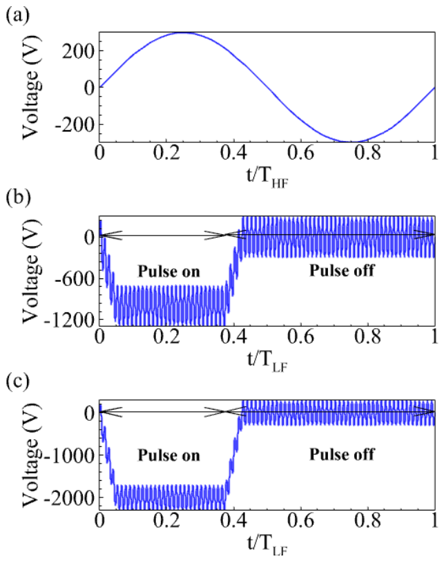
Figure 3.
Time-averaged plasma potential distributions for focus ring heights of (a, b) Lh=15 mm, (c, d) Lh =20 mm, (e, f) Lh =22 mm, and (g, h) Lh =26 mm. The left column (a, c, e, g) shows the full simulation domain, with the peak plasma potential value indicated in each panel. The right column (b, d, f, h) shows enlarged views of the wafer-edge and focus ring region. Equipotential lines are included in all panels.
Figure 3.
Time-averaged plasma potential distributions for focus ring heights of (a, b) Lh=15 mm, (c, d) Lh =20 mm, (e, f) Lh =22 mm, and (g, h) Lh =26 mm. The left column (a, c, e, g) shows the full simulation domain, with the peak plasma potential value indicated in each panel. The right column (b, d, f, h) shows enlarged views of the wafer-edge and focus ring region. Equipotential lines are included in all panels.
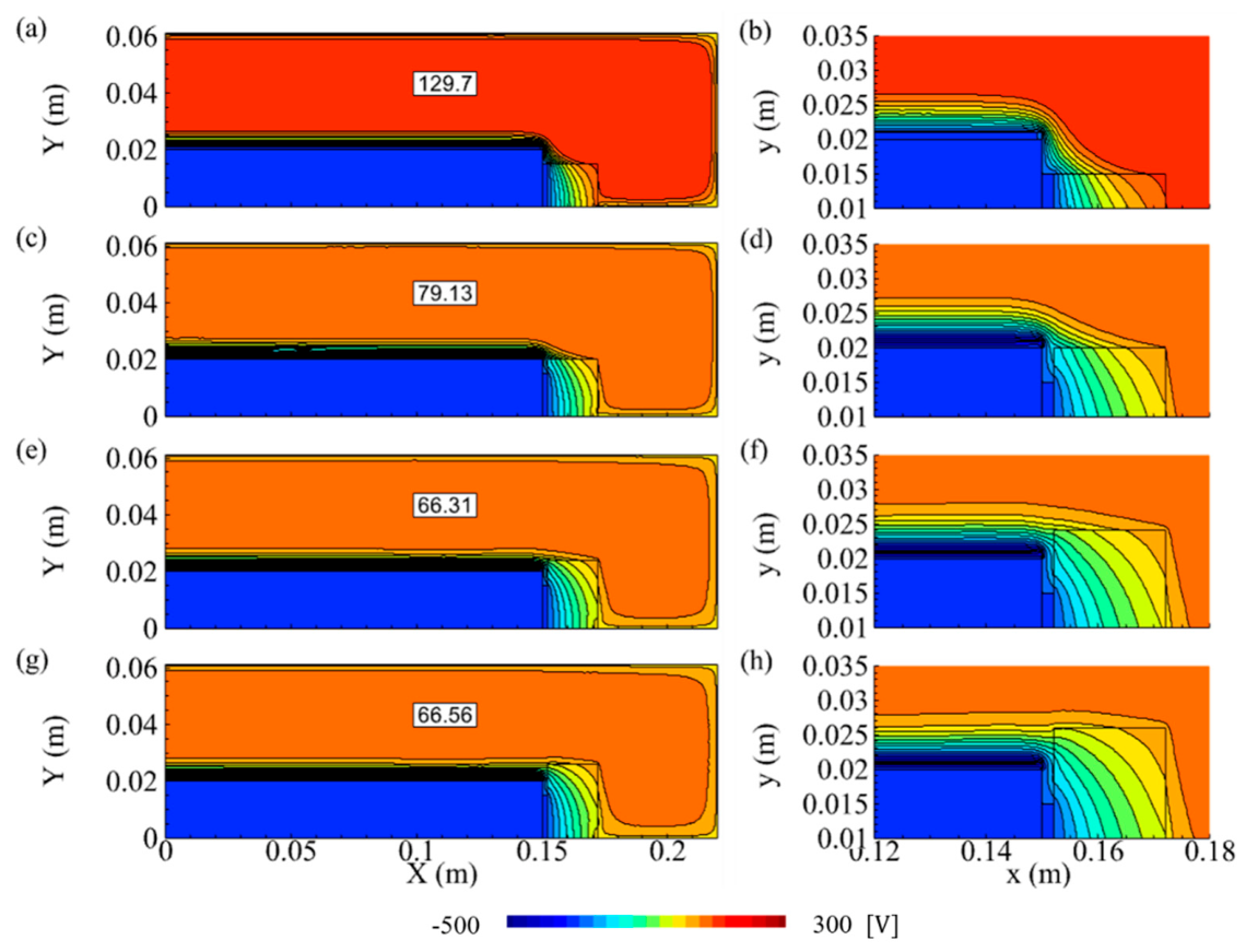
Figure 4.
Time-averaged ion energy-angle distributions (IEADs) at the wafer center and wafer edge for focus ring heights of Lh=15, 20, 22, and 26 mm. (a) wafer center, Lh =15 mm; (b) wafer edge, Lh =15 mm; (c) wafer center, Lh =20 mm; (d) wafer edge, Lh =20 mm; (e) wafer center, Lh =22 mm; (f) wafer edge, Lh =22 mm; (g) wafer center, Lh =26 mm; (h) wafer edge, Lh =26 mm. The color scale is normalized to the maximum value of each distribution and displayed on a logarithmic scale. Positive angles indicate ions defected toward the focus ring side.
Figure 4.
Time-averaged ion energy-angle distributions (IEADs) at the wafer center and wafer edge for focus ring heights of Lh=15, 20, 22, and 26 mm. (a) wafer center, Lh =15 mm; (b) wafer edge, Lh =15 mm; (c) wafer center, Lh =20 mm; (d) wafer edge, Lh =20 mm; (e) wafer center, Lh =22 mm; (f) wafer edge, Lh =22 mm; (g) wafer center, Lh =26 mm; (h) wafer edge, Lh =26 mm. The color scale is normalized to the maximum value of each distribution and displayed on a logarithmic scale. Positive angles indicate ions defected toward the focus ring side.
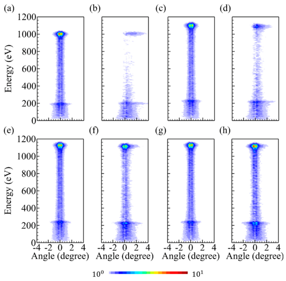
Figure 5.
Time-averaged electron density distributions for focus ring heights of (a) Lh= 15 mm, (b) Lh= 20 mm, (c) Lh= 22 mm, and (d) Lh= 26 mm. The color scale is normalized to the peak electron density of each case, and the peak value is indicated in each panel. (e) one-dimensional electron density profiles along the wafer surface for all four cases. The percentage values indicate the density differences between cases showing similar trends at the wafer center (~0.25 %), in the bulk plasma region (~16.12 %), and near the wafer edge (~39.39 %).
Figure 5.
Time-averaged electron density distributions for focus ring heights of (a) Lh= 15 mm, (b) Lh= 20 mm, (c) Lh= 22 mm, and (d) Lh= 26 mm. The color scale is normalized to the peak electron density of each case, and the peak value is indicated in each panel. (e) one-dimensional electron density profiles along the wafer surface for all four cases. The percentage values indicate the density differences between cases showing similar trends at the wafer center (~0.25 %), in the bulk plasma region (~16.12 %), and near the wafer edge (~39.39 %).
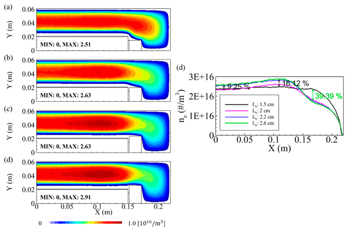
Figure 6.
Time-average distributions of the x-direction electric field, Ex, x-direction ion flux, and electron power absorption, , near the wafer edge-focus ring region for different focus ring height. The rows correspond to Lh= 15, 20, 22, and 26 mm, respectively: (a-c) Lh= 15 mm, (d-f) Lh= 20 mm, (g-i) Lh= 22 mm, and (j-l) Lh= 26 mm. Within each row, the left, middle, and right panels show Ex, x-direction ion flux, and , respectively. The distributions highlight the change in local field structure and power absorption near the wafer edge as the focus ring height is varied.
Figure 6.
Time-average distributions of the x-direction electric field, Ex, x-direction ion flux, and electron power absorption, , near the wafer edge-focus ring region for different focus ring height. The rows correspond to Lh= 15, 20, 22, and 26 mm, respectively: (a-c) Lh= 15 mm, (d-f) Lh= 20 mm, (g-i) Lh= 22 mm, and (j-l) Lh= 26 mm. Within each row, the left, middle, and right panels show Ex, x-direction ion flux, and , respectively. The distributions highlight the change in local field structure and power absorption near the wafer edge as the focus ring height is varied.
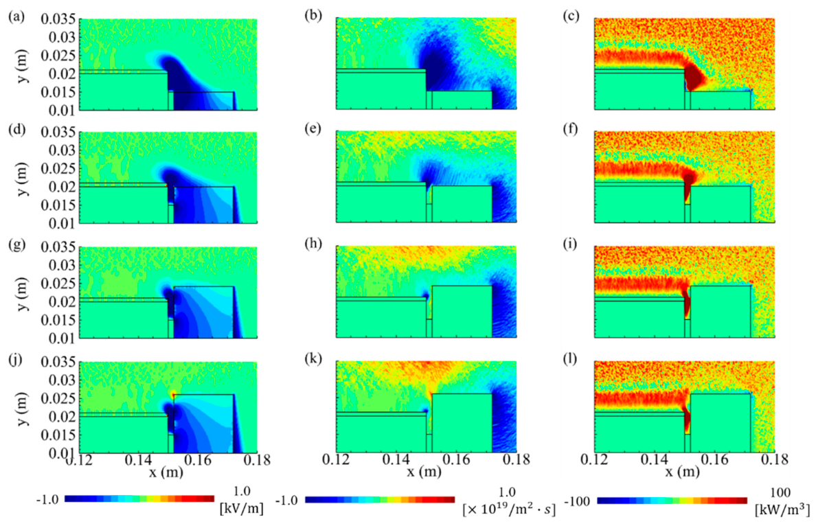
Figure 7.
Time-averaged plasma potential distributions for different electrode-to-focus ring gap widths: (a, b) Lw= 4 mm, (c, d) Lw= 6 mm, (e, f) Lw= 8 mm, and (g, h) Lw= 10 mm. The left-column panels (a, c, e, g) show the full simulation domain, with the maximum plasma potential indicated in each case, while the right-column panels (b, d, f, h) show enlarged vies of the wafer edge/focus ring region. The color scale is fixed from -500 to 300 V for all panels, and equipotential lines are overlaid to visualize the local sheath structure.
Figure 7.
Time-averaged plasma potential distributions for different electrode-to-focus ring gap widths: (a, b) Lw= 4 mm, (c, d) Lw= 6 mm, (e, f) Lw= 8 mm, and (g, h) Lw= 10 mm. The left-column panels (a, c, e, g) show the full simulation domain, with the maximum plasma potential indicated in each case, while the right-column panels (b, d, f, h) show enlarged vies of the wafer edge/focus ring region. The color scale is fixed from -500 to 300 V for all panels, and equipotential lines are overlaid to visualize the local sheath structure.
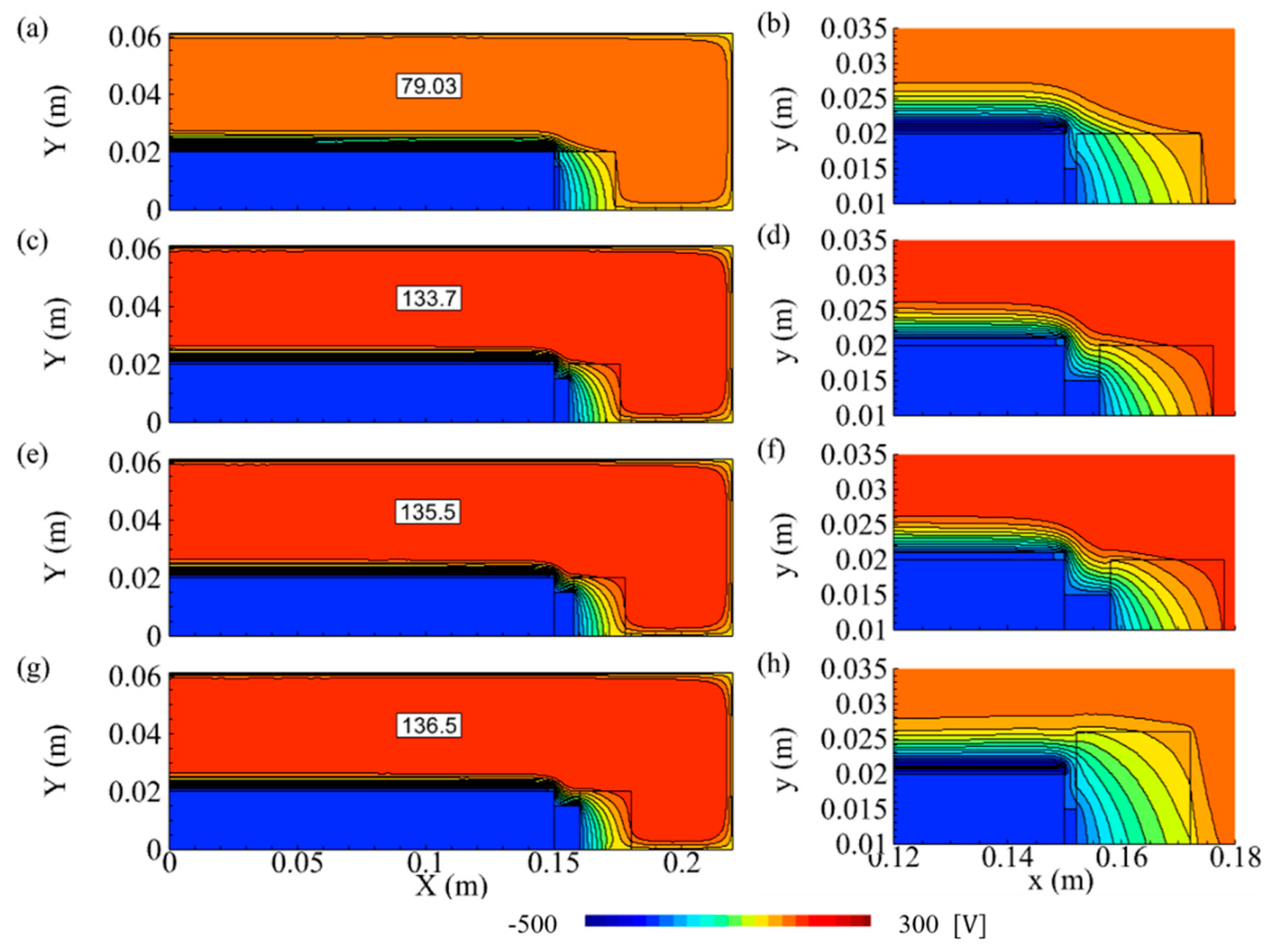
Figure 10.
Time-averaged electron density distributions for focus ring relative permittivity of (a) (quartz) and (b) (Al2O3). Each two-dimensional map is normalized by the maximum electron density of the corresponding case to emphasize the spatial redistribution of the plasma, and the absolute maximum value is indicated in each panel. (c) Time-averaged one-dimensional electron density profiles extracted along the wafer surface for both permittivity cases. The percentage value denotes the maximum relative difference between the two profiles across the wafer surface.
Figure 10.
Time-averaged electron density distributions for focus ring relative permittivity of (a) (quartz) and (b) (Al2O3). Each two-dimensional map is normalized by the maximum electron density of the corresponding case to emphasize the spatial redistribution of the plasma, and the absolute maximum value is indicated in each panel. (c) Time-averaged one-dimensional electron density profiles extracted along the wafer surface for both permittivity cases. The percentage value denotes the maximum relative difference between the two profiles across the wafer surface.
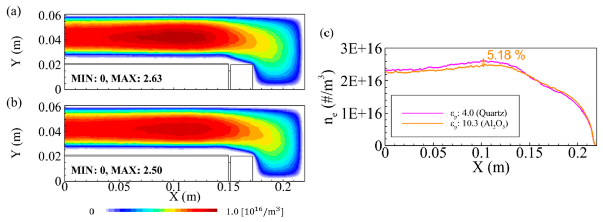
Figure 11.
Time-averaged plasma potential distributions for focus ring relative permittivity of (a, b) (quartz) and (c, d) (Al2O3). The left-column panels (a, c) show the full simulation domain, with the maximum plasma potential indicated in each case, while the right-column panels (b, d) show enlarged views of the wafer edge-focus ring region. The color scale is fixed from -400 to 400 V for all panels to allow direct comparison between the two permittivity cases, and equipotential lines are overlaid to visualize the local sheath structure near the wafer edge and focus ring.
Figure 11.
Time-averaged plasma potential distributions for focus ring relative permittivity of (a, b) (quartz) and (c, d) (Al2O3). The left-column panels (a, c) show the full simulation domain, with the maximum plasma potential indicated in each case, while the right-column panels (b, d) show enlarged views of the wafer edge-focus ring region. The color scale is fixed from -400 to 400 V for all panels to allow direct comparison between the two permittivity cases, and equipotential lines are overlaid to visualize the local sheath structure near the wafer edge and focus ring.
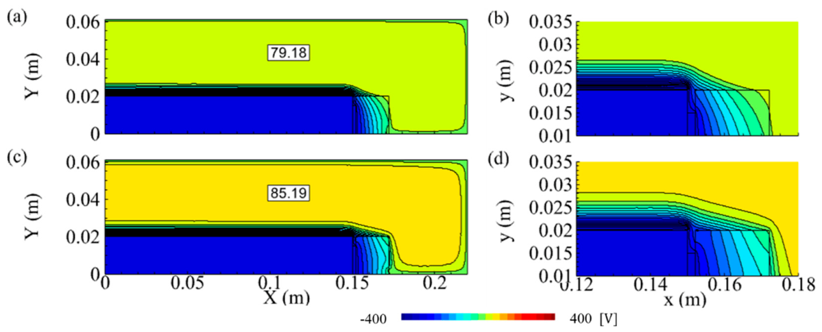
Figure 12.
Time-averaged ion energy-angle distributions (IEADs) at the wafer center and wafer edge, and time-averaged ion energy distribution functions (IEDFs) at the wafer edge, for focus ring relative permittivity of (quartz) and (Al2O3). Panels (a, b) correspond to , and panels (c, d) correspond to (Al2O3); for each case, the left panel shows the IEAD at the wafer center and the right panel shows the IEAD at the wafer edge. Panel (e) compares the wafer edge IEDFs for the two permittivity cases. The color scale in panels (a-d) is normalized to the maximum value of each IEAD.
Figure 12.
Time-averaged ion energy-angle distributions (IEADs) at the wafer center and wafer edge, and time-averaged ion energy distribution functions (IEDFs) at the wafer edge, for focus ring relative permittivity of (quartz) and (Al2O3). Panels (a, b) correspond to , and panels (c, d) correspond to (Al2O3); for each case, the left panel shows the IEAD at the wafer center and the right panel shows the IEAD at the wafer edge. Panel (e) compares the wafer edge IEDFs for the two permittivity cases. The color scale in panels (a-d) is normalized to the maximum value of each IEAD.
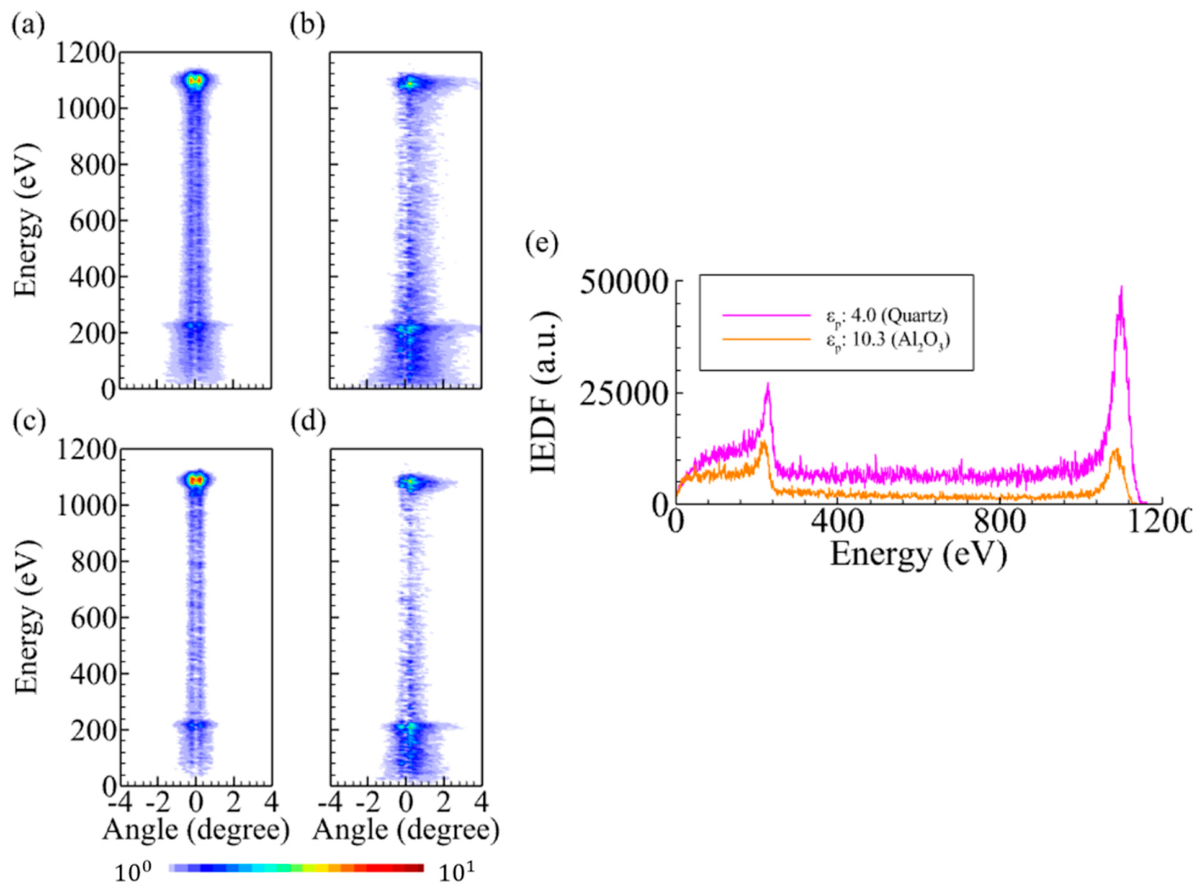
Figure 13.
Time-averaged distributions of the x-direction electric field, Ex, x-direction ion flux, and electron power absorption, , in the wafer edge-focus ring region for focus ring relative permittivity of (quartz) and (Al2O3). The rows correspond to the two permittivity cases: (a-c) and (d-f) . Within each row, the left, middle, and right panels show Ex, x-direction ion flux, and , respectively.
Figure 13.
Time-averaged distributions of the x-direction electric field, Ex, x-direction ion flux, and electron power absorption, , in the wafer edge-focus ring region for focus ring relative permittivity of (quartz) and (Al2O3). The rows correspond to the two permittivity cases: (a-c) and (d-f) . Within each row, the left, middle, and right panels show Ex, x-direction ion flux, and , respectively.
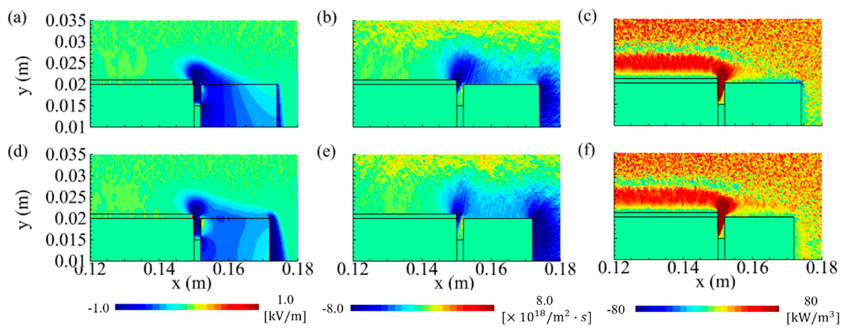
Figure 14.
Time-average electron density distributions for (a) the single frequency (SF) condition () and (b) the enhanced Pulsed DF condition (. The minimum and maximum values of the electron density are indicated in each panel. (c) One-dimensional electron density profiles along the wafer surface for the SF (), baseline Pulsed DF (), and enhanced Pulsed DF () conditions. The baseline Pulsed DF profile is included in (c) to compare the change in electron density with increasing LF voltage magnitude. The percentage values indicate the differences in electron density between selected conditions at representative positions along the wafer surface.
Figure 14.
Time-average electron density distributions for (a) the single frequency (SF) condition () and (b) the enhanced Pulsed DF condition (. The minimum and maximum values of the electron density are indicated in each panel. (c) One-dimensional electron density profiles along the wafer surface for the SF (), baseline Pulsed DF (), and enhanced Pulsed DF () conditions. The baseline Pulsed DF profile is included in (c) to compare the change in electron density with increasing LF voltage magnitude. The percentage values indicate the differences in electron density between selected conditions at representative positions along the wafer surface.
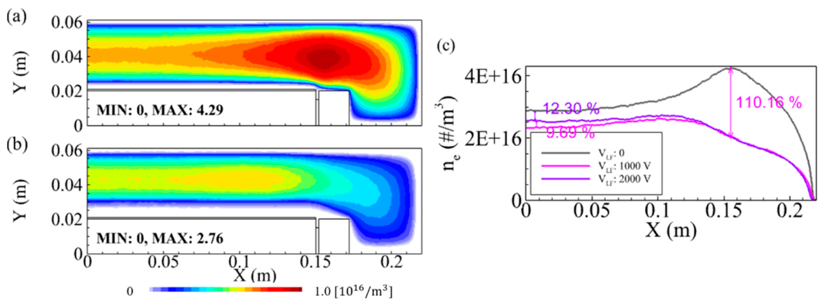
Figure 15.
Time-averaged plasma potential distributions for the (a, b) SF condition () and (c, d) enhanced Pulsed DF condition (). The left column (a, c) shows the full simulation domain, with the peak plasma potential value indicated in each panel, and the right column (b, d) shows enlarged vies of the wafer edge-focus ring region. Equipotential lines are included in all panels.
Figure 15.
Time-averaged plasma potential distributions for the (a, b) SF condition () and (c, d) enhanced Pulsed DF condition (). The left column (a, c) shows the full simulation domain, with the peak plasma potential value indicated in each panel, and the right column (b, d) shows enlarged vies of the wafer edge-focus ring region. Equipotential lines are included in all panels.
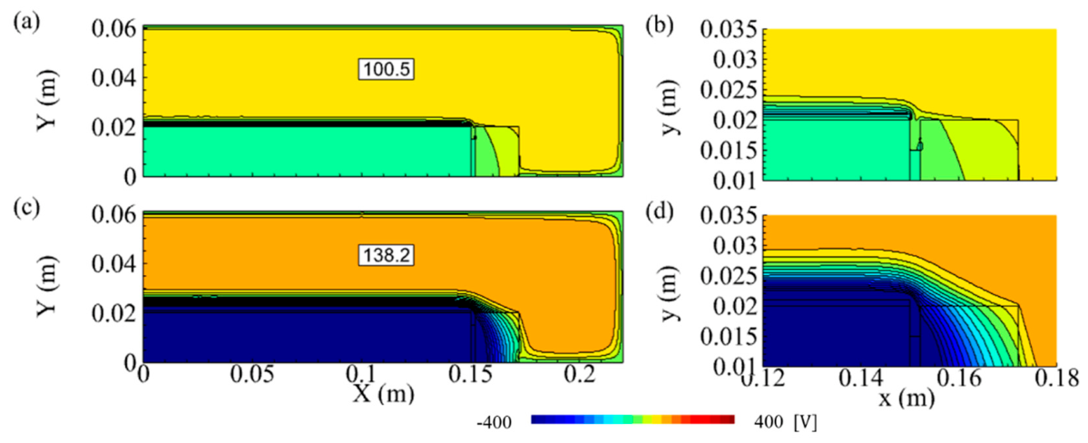
Figure 16.
Time-averaged distributions of (a, d) the x-direction electric field Ex, (b, e) the x-direction ion flux, and (c, f) the electron power absorption term near the wafer edge-focus ring region for (a-c) the SF condition () and (d-f) the enhanced Pulsed DF condition (). The color scales are fixed from to for Ex, from to for the ion flux, and from to for .
Figure 16.
Time-averaged distributions of (a, d) the x-direction electric field Ex, (b, e) the x-direction ion flux, and (c, f) the electron power absorption term near the wafer edge-focus ring region for (a-c) the SF condition () and (d-f) the enhanced Pulsed DF condition (). The color scales are fixed from to for Ex, from to for the ion flux, and from to for .
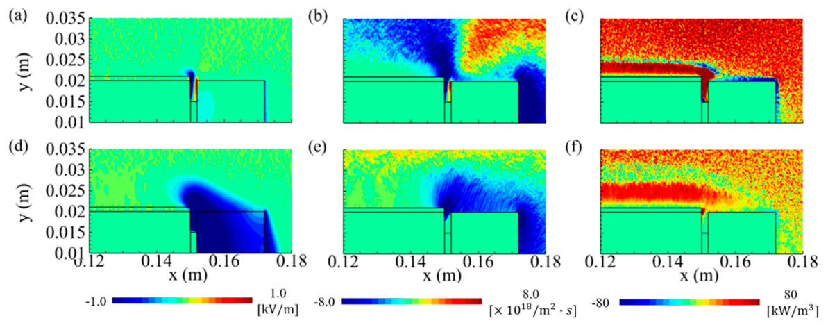

Table 1.
Simulation parameters used in this study.
| Gas type | Argon |
| Pressure | 20 mTorr |
| Grid size (∆x) | 0.2 mm |
| Time step (∆t) | 10 ps |
| Low frequency () | 400 kHz |
| High frequency () | 40 MHz |
| LF voltage () | -1000, -2000 V |
| HF voltage () | 300 V |
| Duty ratio | 0.3 |
| Focus ring height (Lh) | 15, 20, 22, 26 mm |
| Focus ring width (Lw) | 4, 6, 8, 10 mm |
| Relative permittivity of focus ring () | 4.0 (Quartz), 10.3 (Al2O3) |
Disclaimer/Publisher’s Note: The statements, opinions and data contained in all publications are solely those of the individual author(s) and contributor(s) and not of MDPI and/or the editor(s). MDPI and/or the editor(s) disclaim responsibility for any injury to people or property resulting from any ideas, methods, instructions or products referred to in the content. |
© 2026 by the authors. Licensee MDPI, Basel, Switzerland. This article is an open access article distributed under the terms and conditions of the Creative Commons Attribution (CC BY) license.
Copyright: This open access article is published under a Creative Commons CC BY 4.0 license, which permit the free download, distribution, and reuse, provided that the author and preprint are cited in any reuse.


