

Submitted:
10 July 2026
Posted:
14 July 2026
You are already at the latest version
Abstract
RF MEMS switches are key components in an all-passive tunable high-frequency system. In this paper, a compact dual-band antenna system enabled by a single-pole-double-throw (SPDT) RF MEMS switch is proposed for sensing applications in the C-Band and X-Band. Two planar radiating elements, namely, a conventional patch antenna and a metamaterial-inspired patch embedding complementary split-ring resonators (CSRRs), are integrated within the same footprint and selectively activated through the MEMS switch. The CSRR-loaded antenna introduces additional resonant modes, enabling dual-band operation without increasing the overall system size. A λ/4 impedance transformer ensures smooth electrical matching between the SPDT and the two antennas. Electromagnetic simulations performed with Microwave Office confirm good impedance matching and stable radiation patterns in both switching states, with gain not exceeding 3 dBi, consistent with a low-profile geometry on a silicon substrate. The proposed architecture is particularly suited for reconfigurable differential sensing platforms, where simultaneous access to two frequency bands mitigates environmental drift and improves measurement reliability.
Keywords:
RF MEMS
; metamaterial antennas
; dual-band antennas
; X-band SPDT switches
1. Introduction
RF MEMS switches are now a well-established solution for reconfigurable systems encompassing guided-wave configurations and antennas. The main application is to select a route, such as in phase shifters, delay lines, and resonating structures, or to activate antennas operating at different frequencies [1,2]. The C-band covers the frequency range 4.0–8.0 GHz according to the IEEE definition, whereas in the context of 5G and satellite communications, it is conventionally restricted to the 3.7–4.2 GHz sub-band, enabling higher data rates and lower latency than lower-frequency bands. The X-band (8.0–12.0 GHz) is primarily used in radar, satellite, and defense applications, offering higher spatial resolution and improved sensitivity than lower-frequency bands. Dual-band operation spanning these two ranges is therefore of particular interest for sensing platforms that require simultaneous or switchable access to distinct spectral windows, enabling differential measurements and improved robustness to environmental interference.
In this paper, the design of a dual-band antenna based on a single-pole-double-throw (SPDT) RF MEMS structure, which has already been used to select planar resonators, is proposed and discussed. A patch and its variation, made with a metamaterial (MM) geometry, namely complementary split-ring resonators (CSRRs) embedded in the patch, have been connected to each other and separated by an RF MEMS SPDT to select one of the two antennas and the corresponding frequency. A geometrical and electrical optimization of the entire structure has been performed, including a λ/4 transformer connecting the SPDT to the antennas, to ensure a smooth transition from the miniaturized three-port switch to the antennas. This solution was necessary after optimizing every single element of the system, which is characterized by its own size due to the technology on one side and the antenna dimensions at the given frequency on the other.
The choice of a metamaterial (MM) structure was inspired by the need to operate at the building-block level of the entire antenna system, providing greater internal complexity that enables a spectral response with modes that are not far apart. A similar response can be obtained using a different patch side length, but this solution involves a drastic change in patch size and asymmetric configurations. Thus, maintaining symmetry and searching for frequencies within the same band or differing by a small factor, not exceeding a factor of two, is more convenient by changing the antenna's internal geometry. Fractal antennas and metamaterial-inspired configurations meet this requirement and might be the ideal solution for switching frequencies, even with multiple ports, not only for dual-band systems. Despite the possibility of tuning the antenna frequency and beam steering electronically, a fully passive solution remains appealing when the overall size of the structure can be kept within reasonable planar bounds. For this reason, several antennas and planar resonators have been reported in the scientific literature, inspired by different mathematical solutions, such as Sierpinski geometry [3] or complementary split-ring resonators [4] revisited with many internal variations of the metal pattern. In particular, the combination of the split-ring geometry with patch antennas appears very promising for tuning the frequency of simple patches and for portable devices with simple designs and low or null power consumption, as using the RF MEMS solution can be advantageous.
2. SPDT Metamaterial Antenna Design
The complete layout of the designed structure is shown in Figure 1, while the individual components are shown in Figure 2.
The actual realization of the structure is quite easy for the antennas, as a one-mask photolithographic process is sufficient for both radiating elements. As is well known, the manufacturing process for an RF MEMS is more complicated because an eight-mask process, typically ending with sacrificial-layer removal to free a standing metal beam for electrostatic actuation, is required. Several papers and books have been published on MEMS fabrication, encompassing silicon, GaAs, SU-8 polymer materials, and other technologies, like, for instance, [5,6,7].
At this stage, we oversimplified the proposed simulation structure based on our past experience with electromagnetic simulations of RF MEMS switches.
Actually, we considered the switch in the up position to be the open state, while the actuated state is well approximated by a flat metal beam directly on the substrate, touching the lateral pads. Additional elements, such as feeding lines for actuation, or specific details, such as holes in the beam for efficient removal of the sacrificial layer, do not provide deeper insight into the structure's operating principles, and only some additional losses would be considered in a practical experimental case. A 3 µm gap between the metal beam and the substrate surface is practically equivalent to having no interaction with the signal line, or additional losses due to the MEMS geometry, and our SPDT configuration is the usual one already designed and manufactured for redundancy purposes in space applications, while here it is considered again for switching between two kinds of antennas with a sensor meaning.
The left side of the structure shown in Figure 1 is a metamaterial-inspired antenna, the same size as the conventional patch antenna on the right, featuring CSRRs that excite additional modes and shift the resonant frequency. The patch antenna has dimensions of 4.1 x 4.8 mm2. The maximum length of CSRRs is 1.5 mm, and the minimum length of the ring is 1.2 mm in terms of the miniaturization system. The footprint of the entire SPDT antenna system is 24 × 6 mm².
The entire structure has been electromagnetically simulated using release 25.1 of the CADENCE Microwave Office commercial software, implemented via the method of moments with surface currents.
The simulation substrate comprises a 525 µm-thick silicon wafer with a 1 µm-thick additional SiO2 layer deposited by thermal evaporation. Usually, antennas for telecommunication applications use substrates with a lower dielectric constant to mitigate the excitation of surface modes and improve the radiation properties. Nevertheless, this study intentionally focuses on miniaturized, low-profile antennas designed for sensing applications rather than classical telecommunication systems, to evaluate their performance before being tested under varying environmental conditions.
A dual-band architecture is particularly advantageous, for instance, for CO₂ sensing applications, as it enables differential measurements between a reference band and a sensing band, thereby mitigating the effects of environmental variations such as temperature, humidity, and mounting conditions [2]. It is shown and discussed in [8] the CO₂ detection using microwave metasurface-based antennas coated with carbon nanotubes, demonstrating that gas-induced dielectric variations produce measurable resonance shifts in the X/Ku-band frequency range. In [8], a carbon-nanotube-coated electromagnetic bandgap (EMBG) resonator operating at microwave frequencies is used to experimentally validate CO₂ sensing via resonance-frequency variations. Metasurface-based antennas integrated with carbon nanotubes for sensing applications, highlighting the suitability of CNT-functionalized microwave structures for detecting environmental changes, was also shown in [9]. A further improvement of the sensing system, using a non-contact microwave sensor that monitors CO₂ and CH₄ interactions with zeolite materials by tracking permittivity-induced shifts in resonant frequency, was reported in [10]. In [11,12] an enhanced CO₂ sensing using nanostructured materials synthesized via microwave-assisted techniques is studied, demonstrating the strong sensitivity of microwave responses to gas adsorption phenomena. Metamaterial loading using resonant inclusions, such as complementary split-ring resonators (CSRRs) and other double-negative or frequency-selective structures, has been shown to improve impedance matching, reduce reflection losses, introduce additional resonant modes, and enhance near-field confinement [13,14].
This paper proposes integrating an RF MEMS SPDT switch with metamaterial-inspired antennas, which is particularly advantageous for environmental biosensing applications by enabling reconfigurable and differential sensing within a compact, fully passive platform. The SPDT architecture allows the selective activation of multiple antenna responses, facilitating reference-based measurements and mitigating environmental drift. At the same time, metamaterial antennas provide enhanced sensitivity to small dielectric perturbations through strong field localization and multi-resonant behavior, making them well-suited for detecting biological or chemical interactions. Together, these features support low-power, miniaturized, and robust sensing systems for environmental monitoring.
3. Simulation results and discussion
In this paragraph, the predicted performance of the SPDT and the individual SPST switches driving the signal to both antennas, as well as the electromagnetic response of the entire configuration, will be discussed. The approximations introduced and the motivations for the procedure to pass from coplanar waveguide to microstrip structures will be detailed. Finally, the performance of the antenna system in terms of its S-parameter response and radiation patterns will be presented.
3.1. Simulation of the SPST MEMS switch
The design of the SPST MEMS switch has been extracted from a configuration originally intended for a coplanar waveguide (CPW) structure. For the above reason, this building block must be analyzed again, taking into account the new approach for implementing the dual antenna system using a microstrip. To maintain the same size and match the SPST, the microstrip has been extended with a λ/4 transformer designed to operate over a bandwidth wide enough to cover the X- and C-frequency regions. The price to be paid is an extension of the individual switch block, but the advantage is that it saves the electromechanical design already tested, which operates efficiently as an ohmic switch over a wide frequency range. To remember, while a shunt switch is intrinsically a narrowband device because of its resonant response, the ohmic counterpart is a wideband device whose electrical performance is dependent only on the quality of the contact resistance between the wings used for closing the RF path and the line bringing the signal. Such a response justifies the choice of an ohmic switch to drive the signal in two possible structures that operate at significantly different frequencies. The switch with the two ports connected via the transformer is shown in Figure 3, together with its predicted S-parameter performance in the two positions “UP” and “DOWN,” corresponding to the open and closed circuits, respectively, and representing the position of the metal beam before and after the application of the DC voltage used to generate the mechanical force to collapse the metal bridge (see Figure 4).
3.2. Evaluation of the SPDT device and its electrical matching
The SPDT (single-pole-double-throw) switch is a three-port device that selects one of the two output ports (2 and 3), with port 1 as the common input, as shown in Figure 2(c). It consists of two SPST (single-pole-single-throw) RF MEMS switches, each providing ohmic contact when the metal membrane is collapsed by an electrostatic force generated by a purposely designed feeding system, thereby closing the gap and completing the circuit. In each switch, a suspended metal beam is anchored to two pedestals positioned laterally with respect to the microstrip that carries the RF signal; the gap in the microstrip must be closed to provide electrical contact and allow the signal to pass. Accordingly, as discussed in the previous section, the MEMS switches used here are of the ohmic type, and the lateral wings visible in the following figures were previously designed to achieve optimal electrical contact with loss levels between -0.2 dB and -0.4 dB [15].
Matching of the SPDT is crucial for predicting the entire two-antenna system and was assessed in detail using a configuration originally designed for coplanar waveguide (CPW) structures, following preliminary evaluations of the single SPST blocks performed in the previous section. As we have established, the advantage of this choice is that an already validated building block can be incorporated into the novel dual-antenna structure without requiring new design criteria or a different size for the single MEMS switches. However, since the original device was developed for CPW devices, it was necessary to reconsider the electrical matching for the microstrips now used for feeding the antennas; a λ/4 transformer accounting for the change in microstrip width was therefore designed at the center of the frequency range of interest, including now all three ports of the SPDT device. As is well known, in a CPW configuration, a three-port device typically requires bridges between the lateral grounds to maintain an effective common ground between the two sides of the central conductor carrying the signal, since crossing lines can otherwise introduce a non-negligible electrical discontinuity. The microstrip studied here, however, ensures matching in its present form, without such bridges, owing to the confinement of the electric field beneath the SPDT structure, the microstrip having a ground plane on the backside of the wafer. This makes the microstrip arrangement a simplified approach for fabricating a MEMS SPDT. The electromagnetic simulation in Figure 5 is representative of the expected performance for the SPDT when the left arm corresponding to port 2 is not actuated, i.e., when the signal should pass only to the right arm, where the switch is closed (port 3). The central part of the SPDT was already shown in Figure 2(c), and its expected performance is shown in Figure 5. The S11 parameter indicates good input matching, with the best performance across the X-Band, while low insertion loss and good isolation are observed between ports 2 and 3. The situation is symmetric when the opposite arm is closed with the actuated MEMS switch. Note that the open state on the left arm (port 2) was initially simulated by placing the metal beam of the switch 3 µm above the wafer surface, but the bridge was subsequently omitted from simulation based on prior theoretical and experimental evidence showing its negligible influence on S-parameters at this distance from the wafer [16]. For this reason, the following antenna system simulations do not include the bridge in the up position, as it has negligible influence on the antenna output.
3.3. Simulation of the individual antennas and the dual-antenna system
The results of the individual antenna simulation are shown in Figure 6, and those of the entire system in Figure 7. Parameter S11, namely the reflection coefficient of the structure, is defined as the ratio of the input to the reflected signal and provides a measure of the antenna's electrical input impedance.
The metamaterial (MM) single antenna has a narrower bandwidth, as expected from its design, and is more susceptible to interference from other RF sections, which can modify the spectrum. Actually, the individual antennas exhibit a single resonance for the simple patch and a multi-resonant response for the MM-inspired patch, due to the additional resonant elements in the latter. A further difference, due to the presence of additional lines and components in the full structure, is a shift in the resonant frequency and modified electrical matching, which enhances one selected resonance in a manner that differs from that of the individual antenna. For this reason, only a full-structure simulation can yield the ultimate result for the antenna's frequency response, even though preliminary simulations were necessary to provide a reasonable prediction of performance in terms of electrical matching, resonant frequency, and bandwidth.
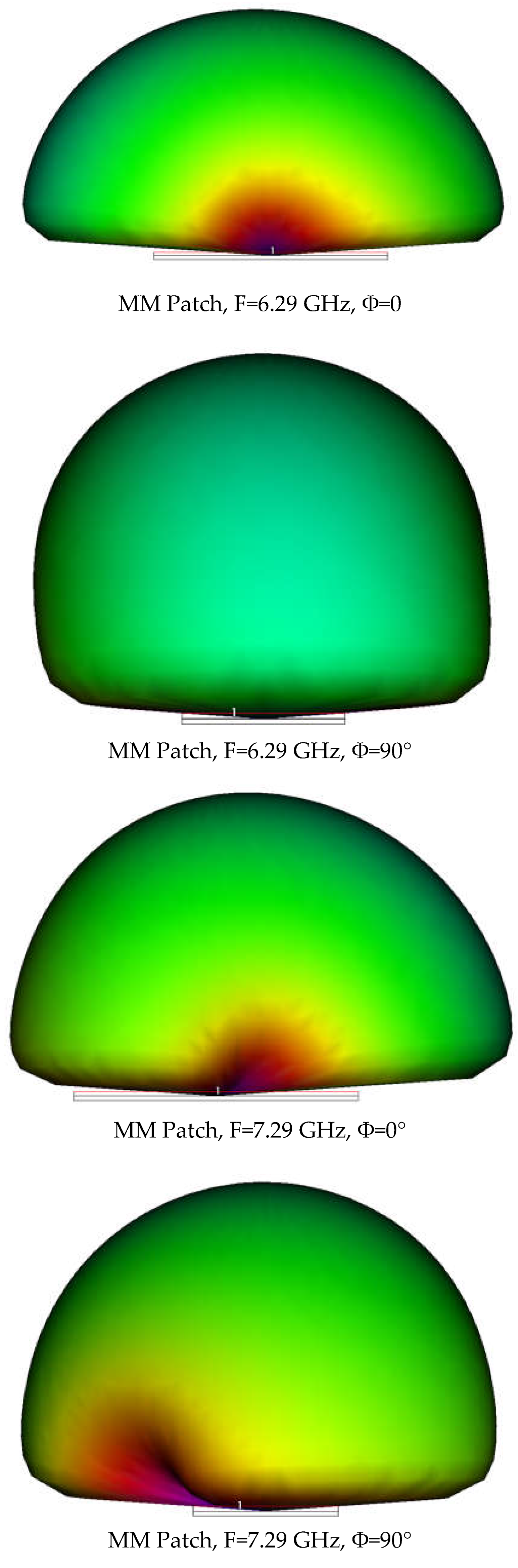
The antenna's radiation pattern in the two possible states is determined by the SPDT actuation on the right side of the RF MEMS device for the simple patch and on the left side for the metamaterial one, as shown in the initial figures of the entire structure. In the following plots, the radiation patterns for both cases are shown, exhibiting moderate-to-low gain, not exceeding 3 dBi, as expected for a low-profile antenna, and are homogeneous in both in-plane views, i.e., at Φ=0° and Φ=90°, when the resonance frequencies are considered. In Figure 8 and Figure 9, three radiation patterns are plotted at the resonance frequencies: F=10.46 GHz (simple patch) and F=6.28 and 7.29 GHz (MM patch). The patterns are plotted for the in-plane angles Φ = 0 ° and Φ = 90 °.
The electromagnetic simulations demonstrate that the proposed architecture enables effective frequency reconfiguration while maintaining acceptable impedance matching and compact dimensions. The metamaterial-inspired antenna introduces additional resonant modes and frequency shifts, enabling dual-band operation without increasing the system's overall size. The use of a silicon-based substrate, while limiting radiation efficiency, underlines the potential of this solution for integrated, low-profile sensing platforms where miniaturization and process compatibility are primary constraints.
The results presented confirm that RF MEMS technology is a viable and efficient approach to realizing all-passive, frequency-agile antenna systems, paving the way for future experimental validation and system-level integration for environmental sensor applications.
As shown in the figures, the radiation pattern profile generated by the dual-antenna system remains unchanged, maintaining the same response when switching via the SPDT RF MEMS.
4. Conclusions
In this paper, a compact dual-band antenna system enabled by an RF MEMS single-pole-double-throw (SPDT) switch has been proposed and investigated for C-band and X-band sensing applications. Two planar radiating elements—a conventional patch antenna and a metamaterial-inspired patch embedding complementary split-ring resonators—have been integrated within the same footprint and selectively activated through the MEMS switch. The proposed technological solution favors implementing antenna systems based on elementary building blocks of the same size but with different operating frequencies, thereby enabling more complex arrangements and, eventually, MEMS multi-pole configurations, in which a few small-sized antennas respond to different frequencies. We conclude that this work extends the applications of RF MEMS technology to control the resonant frequency of a dual-antenna system. Such a finding enables an all-passive system with low or zero power consumption to drive a dual-mode antenna for reconfiguration, allowing differential measurements between a reference and a sensing channel that compensate for environmental drift and improve measurement reliability. Finally, we propose that low-profile antennas on a silicon substrate, not typically used in telecommunications, are well suited for miniaturized non-contact sensing applications. Following this approach, additional frequencies can be considered for a still compact device hosting more antennas, driven by a single-pole-multiple-throw (SPMT) switch.
Supplementary Materials
The following supporting information can be downloaded at the website of this paper posted on Preprints.org. Supporting information is available in this paper.
Author Contributions
Conceptualization, A.M.C., E.P. and R.M.; methodology, R.M.; investigation, A.M.C., E.P. and R.M.; writing—review and editing, R.M.; All authors have read and agreed to the published version of the manuscript.
Funding
This research was funded by two grants of the Romanian Ministry Education and Research, Project- 8N/2023-µNanoEl within ‘’Programul Nucleu”.
Data Availability Statement
All simulation data are available upon requirement.
Conflicts of Interest
The authors declare no conflicts of interest.
Abbreviations
The following abbreviations are used in this manuscript:
| MEMS | Microelectromechanical Systems |
| CSRR | Complementary Split Ring Resonator |
| SPST | Single-Pole-Single-Throw |
| SPDT | Single-Pole-Double-Throw |
| MM | Metamaterial |
References
- Tait, R.N. Progress in RF-MEMS. Micromachines 2025, 16, 233. [Google Scholar] [CrossRef] [PubMed]
- Shao, B.; Lu, C.; Xiang, Y.; Li, F.; Song, M. Comprehensive Review of RF MEMS Switches in Satellite Communications. Sensors 2024, 24, 3135. [Google Scholar] [CrossRef] [PubMed]
- Puente-Baliarda; Romeu, J.; Pous, R.; Cardama, A. On the behavior of the Sierpinski multiband fractal antenna. IEEE Trans. Antennas Propag. 1998, vol. 46(no. 4), 517–524. [Google Scholar] [CrossRef]
- Baena, Juan Domingo; et al. Equivalent-circuit models for split-ring resonators and complementary split-ring resonators coupled to planar transmission lines. IEEE Trans. Microw. Theory Tech. 2005, 53, 1451–1461. [Google Scholar] [CrossRef]
- The MEMS Handbook, Online from the University of California San Diego. 29 June 2026. Available online: https://maecourses.ucsd.edu/~pbandaru/mae268-sp09/Class%20Readings_files/MEMS%20materials.
- Sinha, N.; Mahameed, R.; Zuo, C.; Piazza, G. Integration of AlN micromechanical contour-mode technology filters with three-finger dual beam AlN MEMS switches. 2009 IEEE International Frequency Control Symposium Joint with the 22nd European Frequency and Time forum, Besancon, France, 2009; pp. 1–4. [Google Scholar] [CrossRef]
- Martinez-Duarte, R. SU-8 Photolithography as a Toolbox for Carbon MEMS. Micromachines 2014, 5, 766–782. [Google Scholar] [CrossRef]
- Cismaru; Dragoman, M.; Iordănescu, S.; Obreja, C.; Buiculescu, V.; El Ghannudi, H.; Pârvulescu, C.; Mladenovic, D.; Carp, M.; Brâncoveanu, O. CO₂ detection using microwave metasurface-based antennas covered with carbon nanotubes. Mater. Sci. Eng. B vol. 318, 118282, 2025. [CrossRef]
- Cismaru; Aldrigo, M.; Cosmin Obreja, A.; Dragoman, M.; et al. CNT-based EMBG resonator for CO₂ gas detection. in Proc. 2018 Symp. Design, Test, Integration & Packaging of MEMS/MOEMS (DTIP), 2018; pp. 1–4. [Google Scholar]
- Cismaru; Aldrigo, M.; Iordănescu, S.; Mladenović, D.; et al. Metasurface-based antennas integrated with carbon nanotubes for DNA sensors applications. 2021 IEEE 16th Nanotechnology Materials and Devices Conf. (NMDC), 2021. [Google Scholar] [CrossRef]
- Zarifi, S.; Smith, D. R.; Benson, K. A non-contact microwave sensor for monitoring the interaction of zeolite 13X with CO₂ and CH₄ in gaseous streams. Sens. Actuators B Chem. 2016, vol. 238, 1240–1248. [Google Scholar] [CrossRef]
- Morán-Lázaro, M.; García-Hernández, R.; Rodríguez-Vázquez, J.; et al. Enhanced CO₂-sensing response of nanostructured cobalt aluminate synthesized using a microwave-assisted colloidal method. Sens. Actuators B Chem. 2016, vol. 226, 518–525. [Google Scholar] [CrossRef]
- Rahman, Abdullah Al Mahfazur; Islam, Mohammad Tariqul; Moniruzzaman, Md.; Abdul Rahim, Sharul Kamal; Singh, Mandeep; Misran, Norbahiah; Islam, Md. Shabiul; Soliman, Mohamed S. H-shaped modifiers loaded mirror symmetric resonator based double negative metamaterial for multi-band wireless communications. Sci. Rep. 2023, volume 13, Article number, 15943. [Google Scholar] [CrossRef] [PubMed]
- Cai, Longzhu; Jiang, Zhi Hao; Wu, Jing-Bo; Chen, Hui; Hong, Wei. Low-loss and flexible terahertz bandpass frequency selective surface based on cyclic olefin copolymer substrate via solvent-free synthesis. Opt. Express 2023, Vol. 31(Issue 13), 21706–21720. [Google Scholar] [CrossRef] [PubMed]
- Mulloni, V.; Margesin, B.; Farinelli, P.; et al. Cycling reliability of RF-MEMS switches with Gold–Platinum multilayers as contact material. Microsyst. Technol. 2017, 23, 3843–3850. [Google Scholar] [CrossRef]
- Cismaru, A.; Giacomozzi, F.; Pasteanu, M.; Marcelli, R. Design Optimization of RF MEMS-Driven Triangular Resonators with Sierpinski Geometry for Dual-Band Applications. Micromachines 2025, 16, 446. [Google Scholar] [CrossRef] [PubMed]
Figure 1.
Full structure layouts, electromagnetically simulated using the release 25.1 of the CADENCE Microwave Office commercial software, implemented by means of the method of moments, using surface currents. In (a), the switch is actuated on the right side (simple patch), and in (b), the switch is actuated on the left side (metamaterial patch). The two non-actuated paths are intentionally left open to emulate, in a 2.5D geometry, the designed function of the SPDT.
Figure 1.
Full structure layouts, electromagnetically simulated using the release 25.1 of the CADENCE Microwave Office commercial software, implemented by means of the method of moments, using surface currents. In (a), the switch is actuated on the right side (simple patch), and in (b), the switch is actuated on the left side (metamaterial patch). The two non-actuated paths are intentionally left open to emulate, in a 2.5D geometry, the designed function of the SPDT.
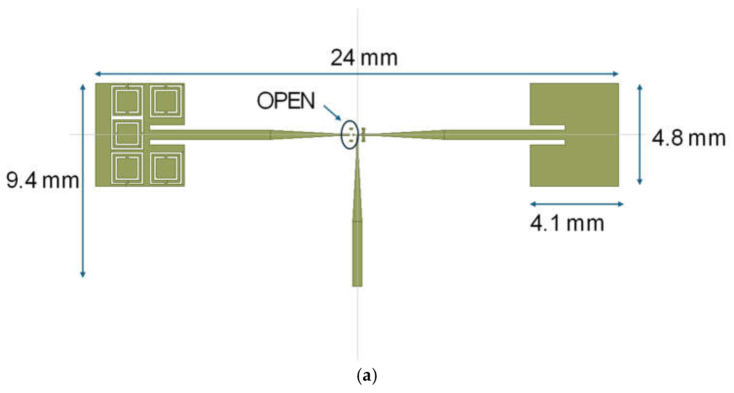
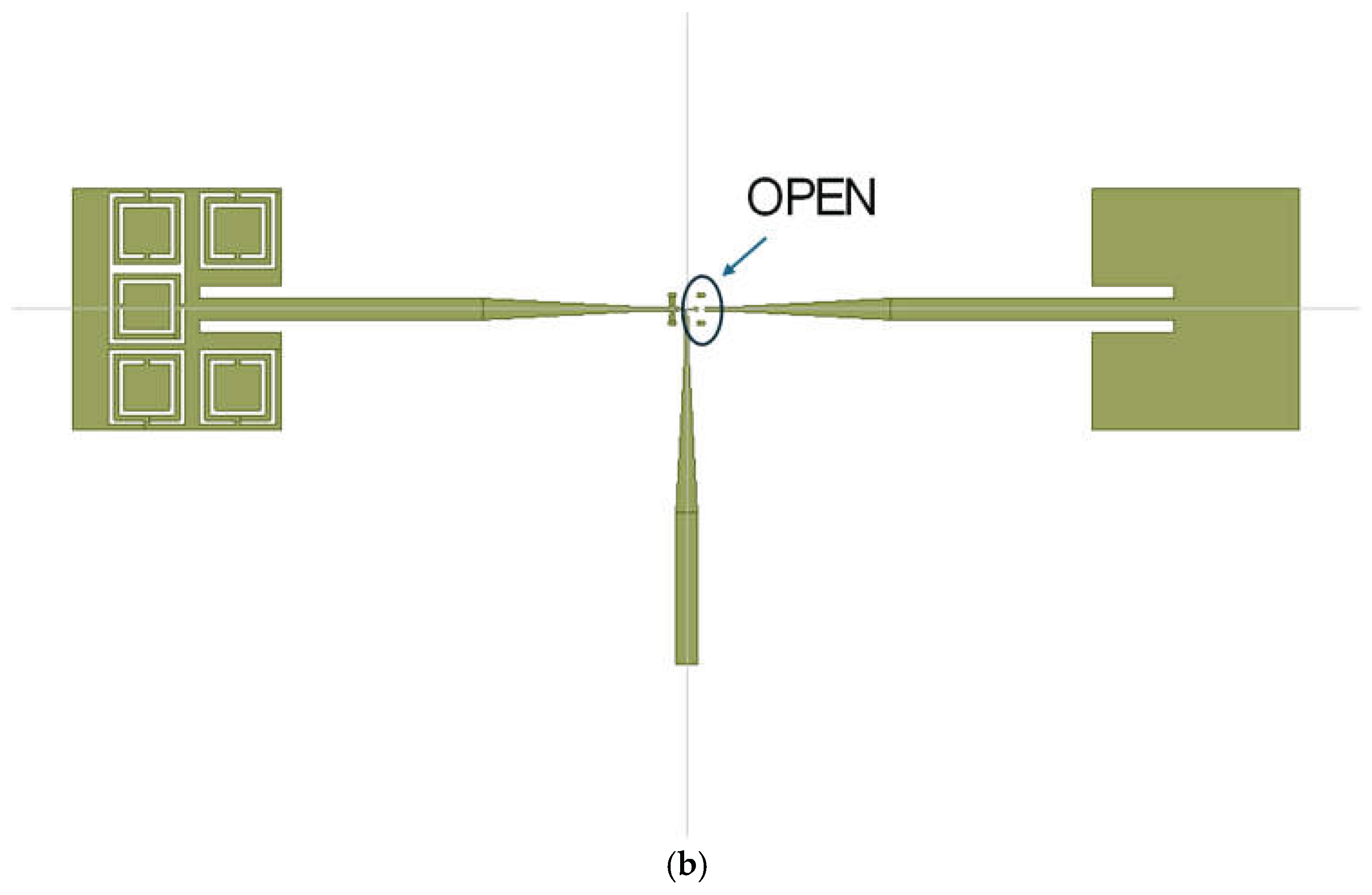
Figure 2.
From top to bottom: Details of the simulated structure, including: (a) the metamaterial patch antenna with split ring resonators inside, (b) the canonical patch antenna, and (c) the SPDT switch geometry. In the bottom figure, the left switch is missing to emulate the up position, while the right one is actuated and approximated with a continuous microstrip line.
Figure 2.
From top to bottom: Details of the simulated structure, including: (a) the metamaterial patch antenna with split ring resonators inside, (b) the canonical patch antenna, and (c) the SPDT switch geometry. In the bottom figure, the left switch is missing to emulate the up position, while the right one is actuated and approximated with a continuous microstrip line.
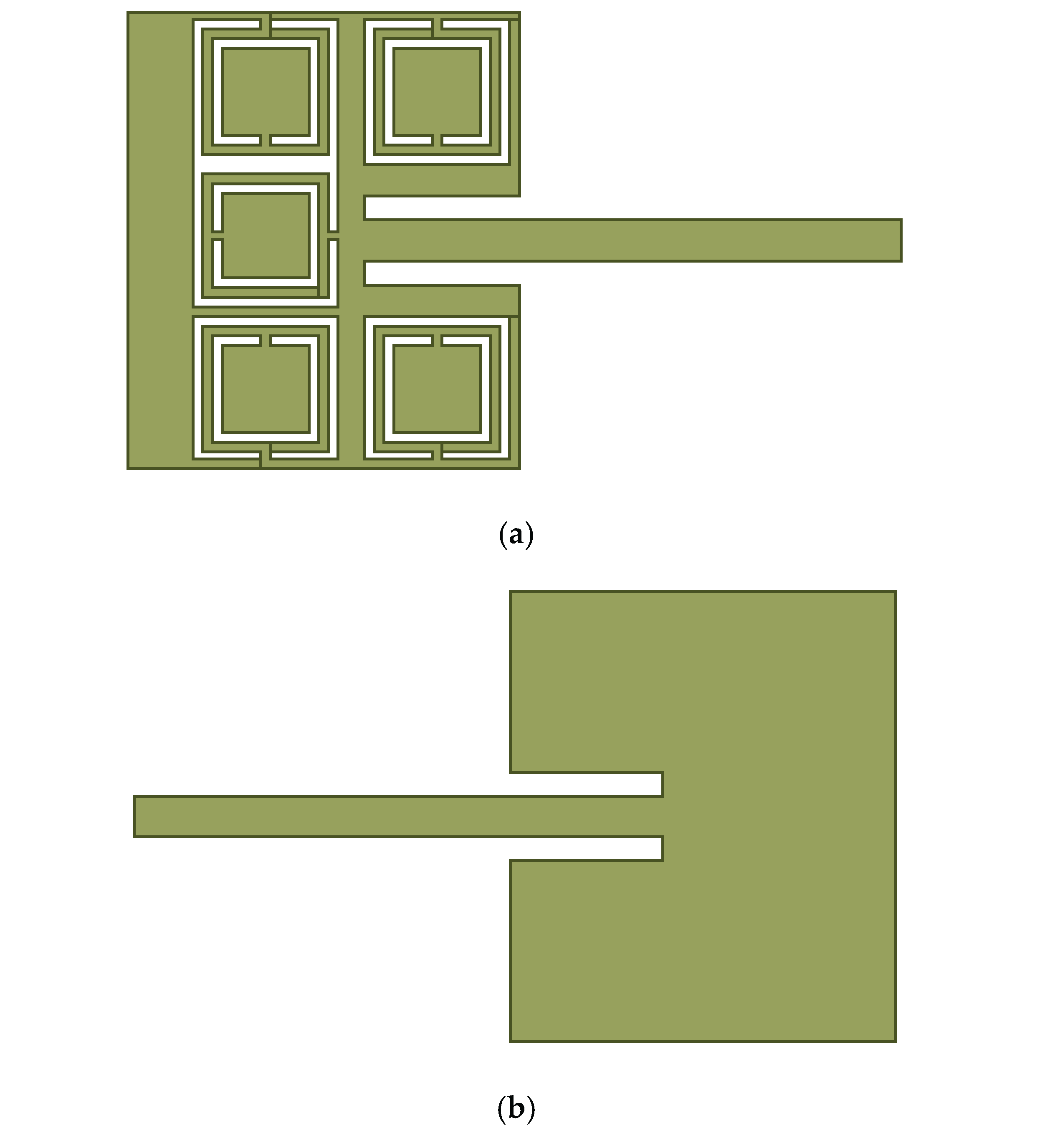
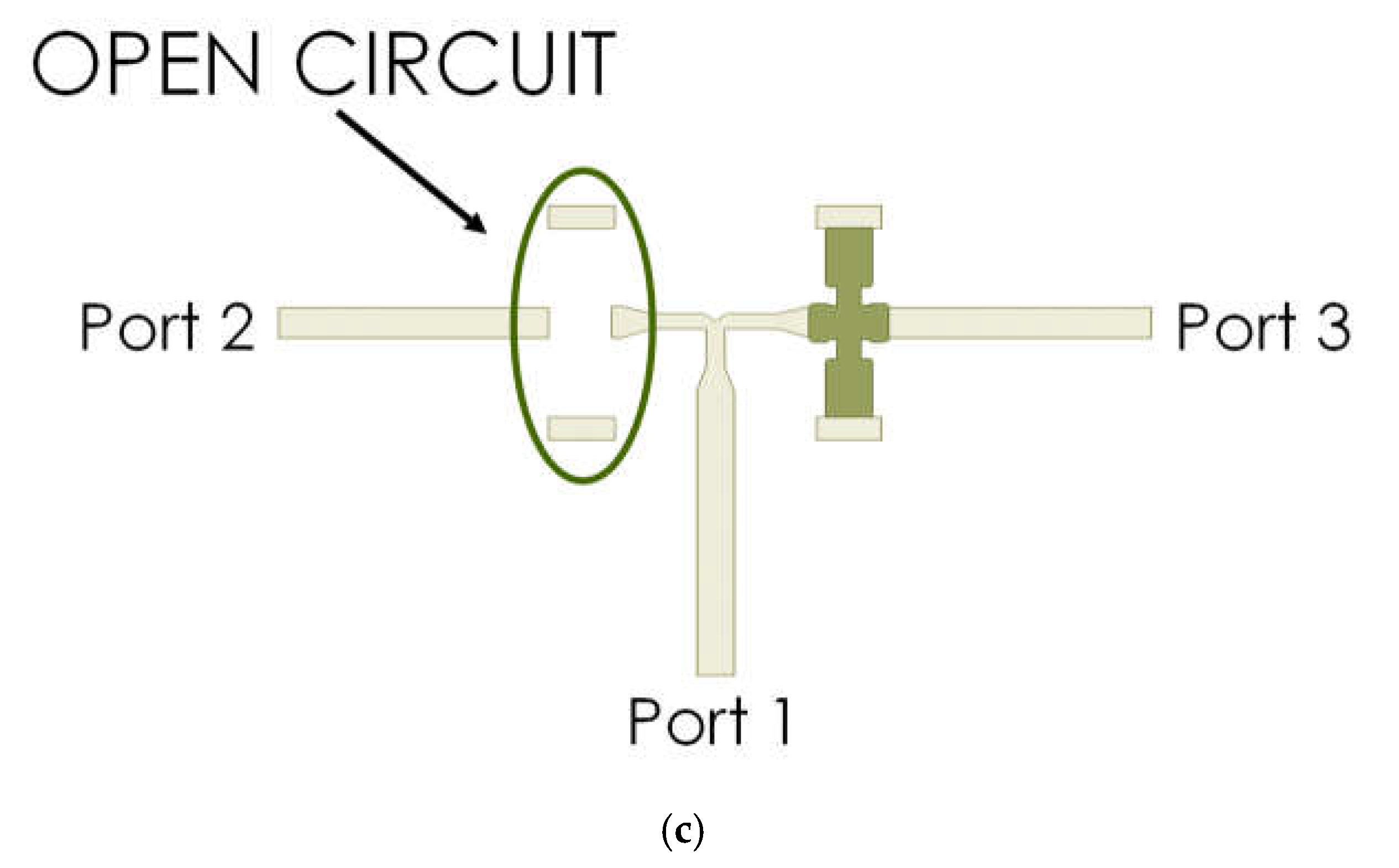
Figure 3.
Configuration of the SPST RF MEMS ohmic switch simulated before its implementation in the SPDT structure (detailed view) and the entire device including the transformer.
Figure 3.
Configuration of the SPST RF MEMS ohmic switch simulated before its implementation in the SPDT structure (detailed view) and the entire device including the transformer.
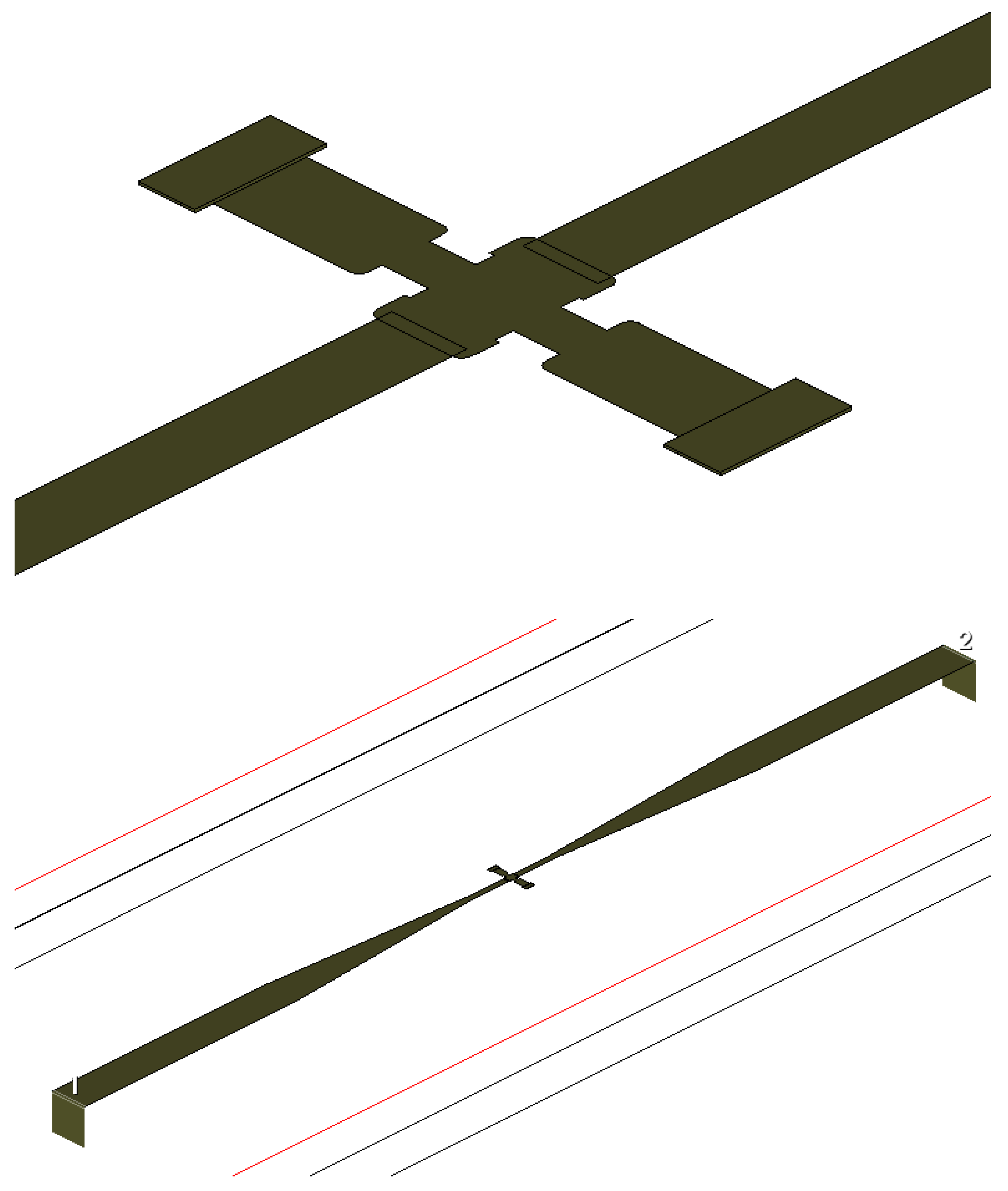
Figure 4.
Predicted performance of the SPST RF MEMS switch in the “UP” and “DOWN” positions, respectively. An isolation better than -20 dB is provided up to the end of the X-band.
Figure 4.
Predicted performance of the SPST RF MEMS switch in the “UP” and “DOWN” positions, respectively. An isolation better than -20 dB is provided up to the end of the X-band.
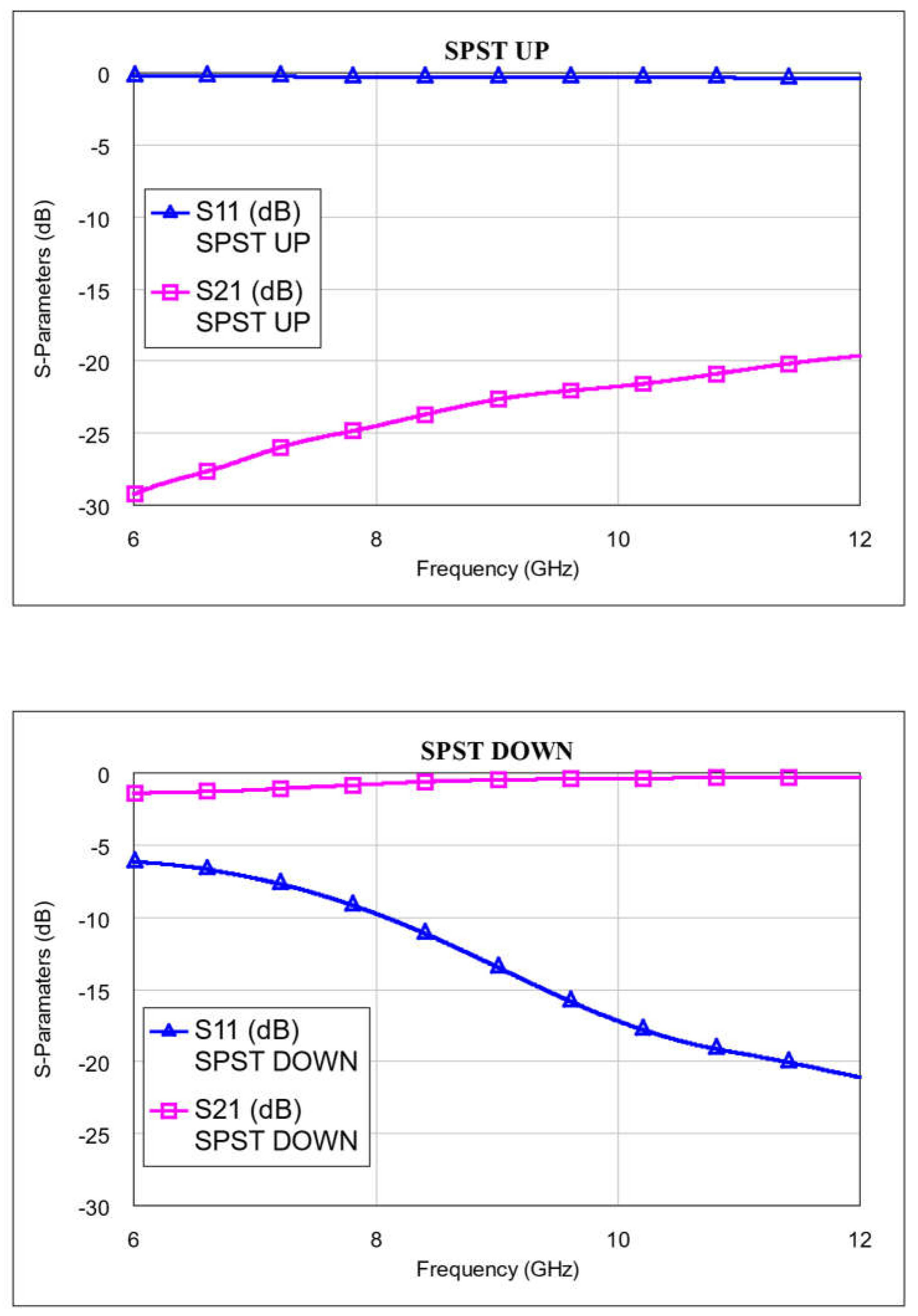
Figure 5.
Performance for the SPDT when the left arm is not actuated, corresponding to the open circuit, while the right one is actuated. In this case, S21 and S32 are very low as no power is transferred between the ports along these paths.
Figure 5.
Performance for the SPDT when the left arm is not actuated, corresponding to the open circuit, while the right one is actuated. In this case, S21 and S32 are very low as no power is transferred between the ports along these paths.
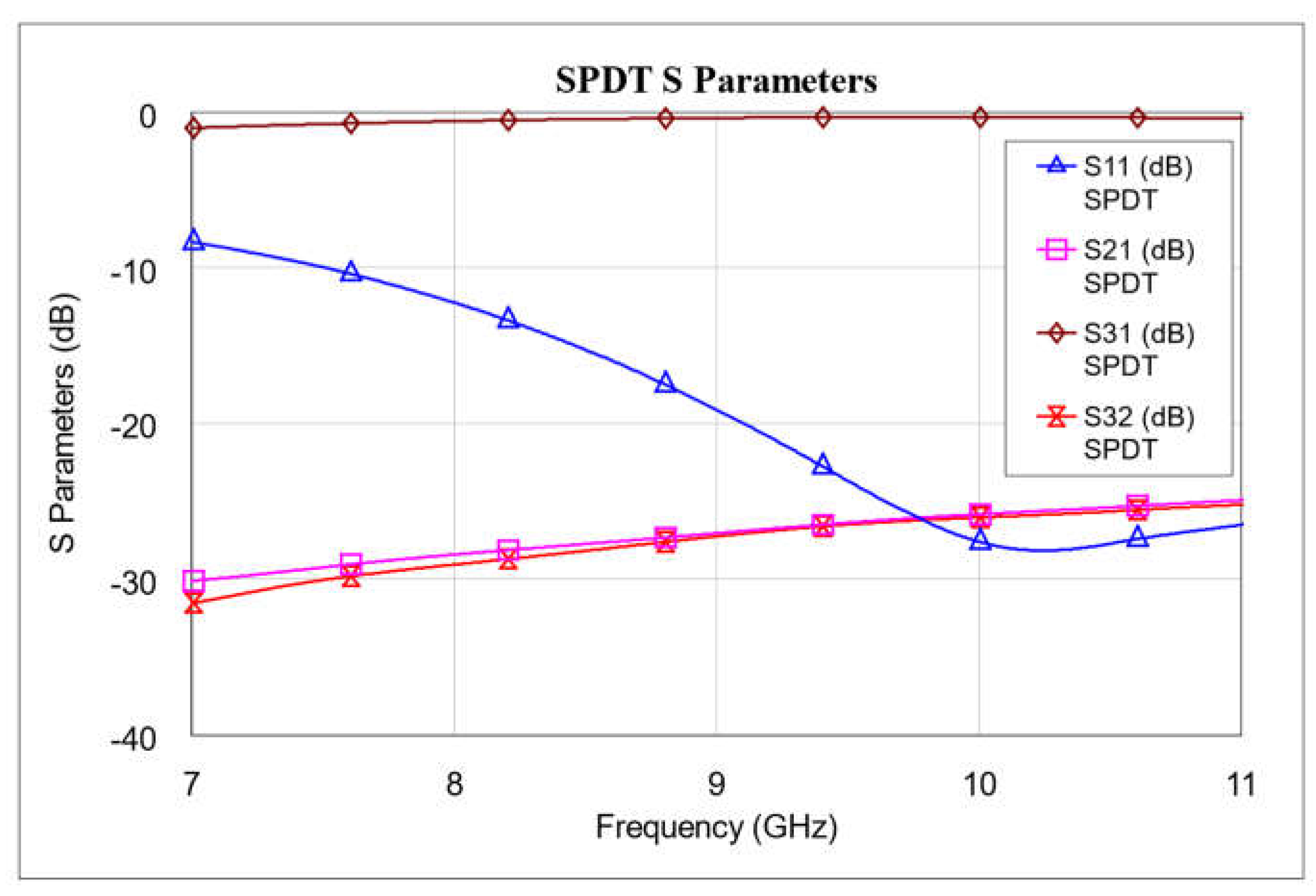
Figure 6.
Electromagnetic simulation of the individual antennas. The simple patch, i.e., the canonical structure with a full metal plate, resonates at a single frequency, whereas the metamaterial (MM) antenna introduces additional frequencies due to split-ring resonators embedded in the patch. The vertical axis is the reflection coefficient S11 (dB).
Figure 6.
Electromagnetic simulation of the individual antennas. The simple patch, i.e., the canonical structure with a full metal plate, resonates at a single frequency, whereas the metamaterial (MM) antenna introduces additional frequencies due to split-ring resonators embedded in the patch. The vertical axis is the reflection coefficient S11 (dB).
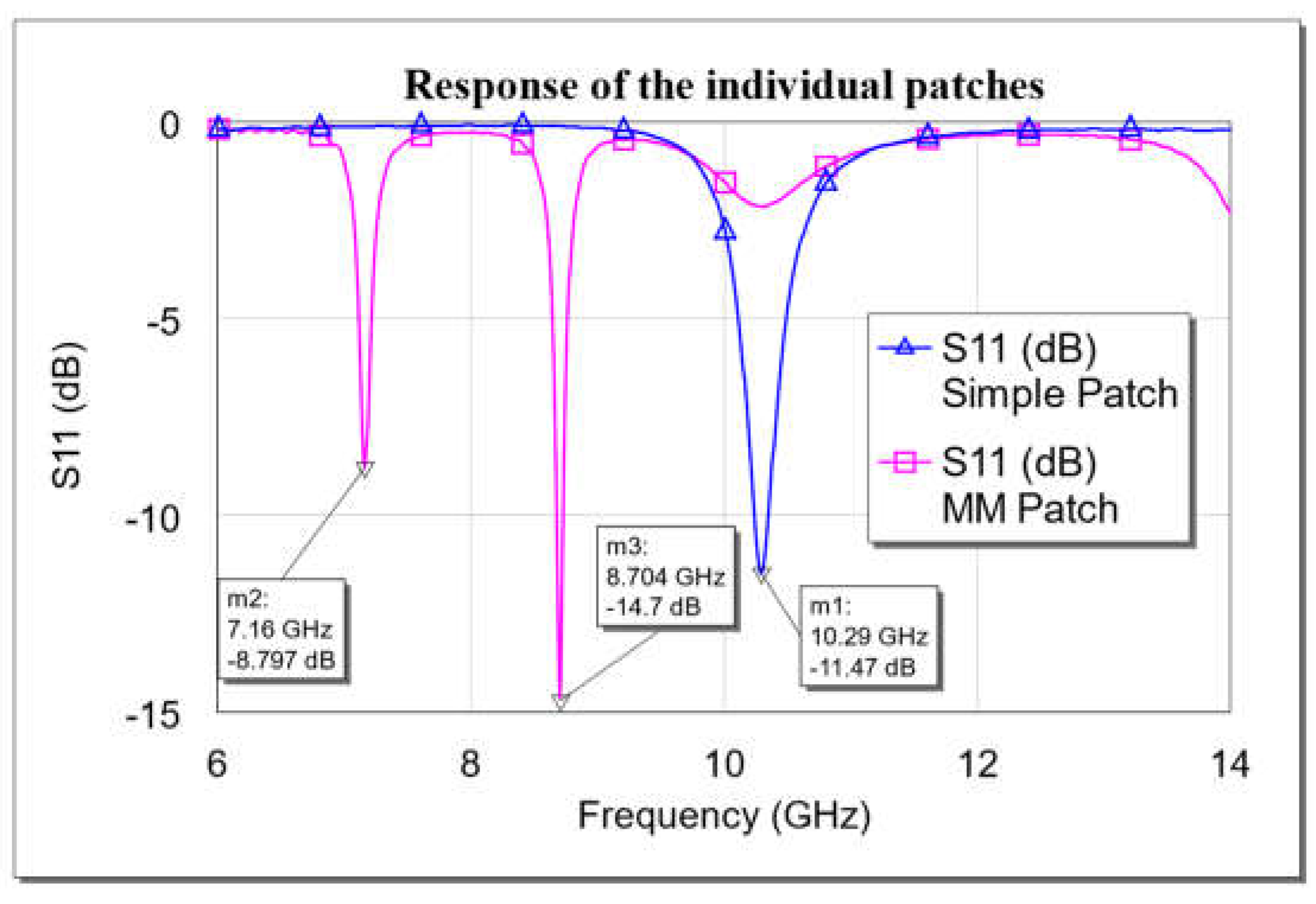
Figure 7.
Electromagnetic simulation of the entire system, switching between the simple patch and the MM antenna. The vertical axis is the reflection coefficient S11 (dB).
Figure 7.
Electromagnetic simulation of the entire system, switching between the simple patch and the MM antenna. The vertical axis is the reflection coefficient S11 (dB).
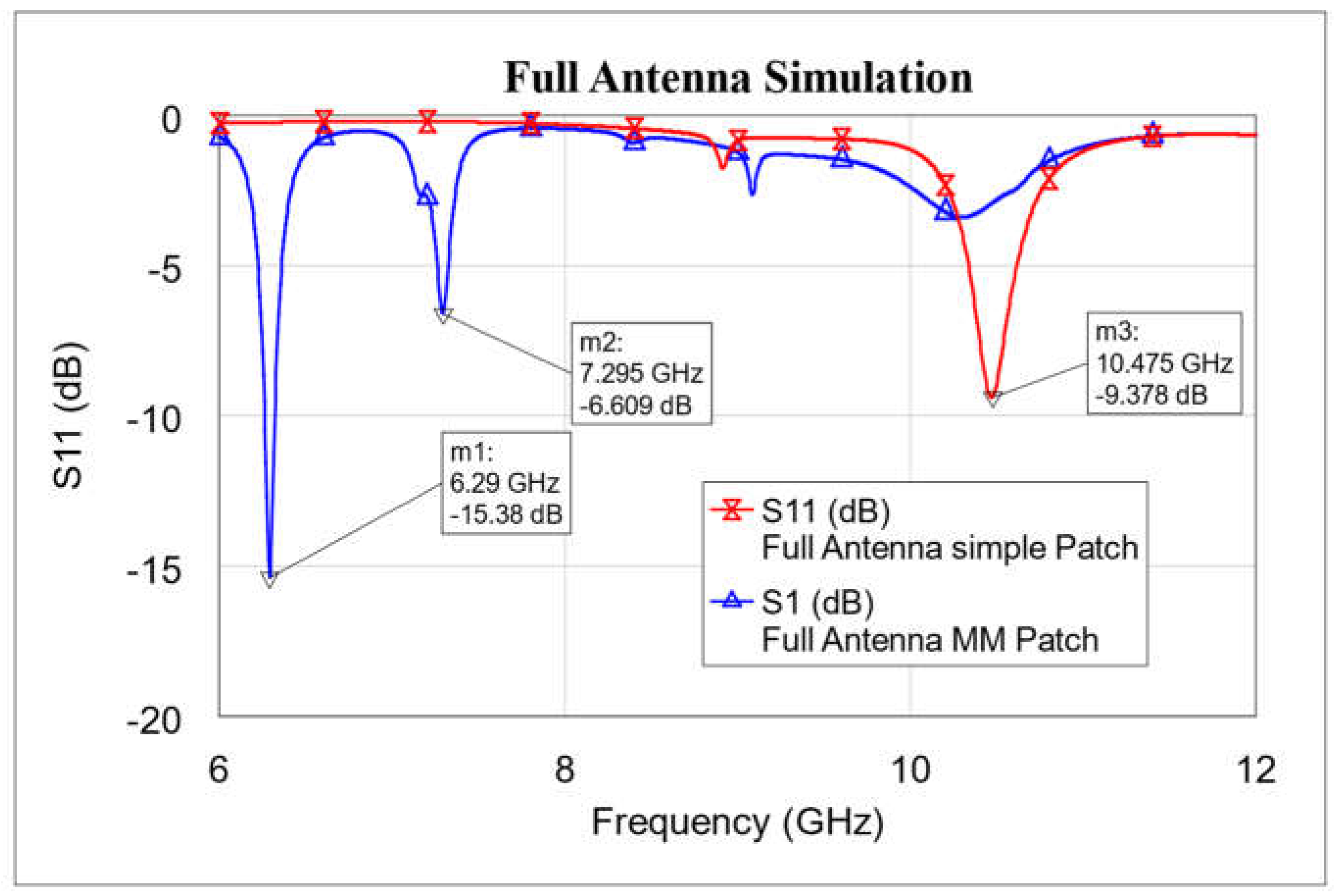
Figure 8.
Electromagnetic radiation of the double antenna, switching the SPDT to the patch antenna.
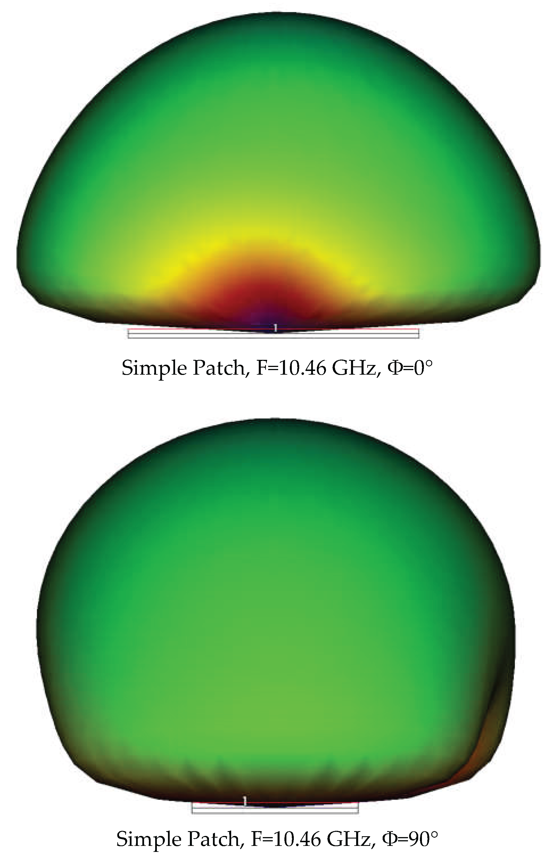
Figure 9.
Electromagnetic radiation pattern, switching the SPDT to the MM antenna.
Disclaimer/Publisher’s Note: The statements, opinions and data contained in all publications are solely those of the individual author(s) and contributor(s) and not of MDPI and/or the editor(s). MDPI and/or the editor(s) disclaim responsibility for any injury to people or property resulting from any ideas, methods, instructions or products referred to in the content. |
© 2026 by the authors. Licensee MDPI, Basel, Switzerland. This article is an open access article distributed under the terms and conditions of the Creative Commons Attribution (CC BY) license (http://creativecommons.org/licenses/by/4.0/).
Copyright: This open access article is published under a Creative Commons CC BY 4.0 license, which permit the free download, distribution, and reuse, provided that the author and preprint are cited in any reuse.


