
Submitted:
07 July 2026
Posted:
09 July 2026
You are already at the latest version
Abstract
Coating technologies are essential for improving material surface properties while preserving
bulk performance. They are widely used to enhance wear resistance, corrosion protection,
thermal stability, biocompatibility, and functional behavior in aerospace, automotive,
biomedical, electronics, and energy applications. Together with conventional electrochemical
methods, the field has advanced to sophisticated techniques such as physical vapour deposition
(PVD), laser cladding, chemical vapour deposition (CVD), atomic layer deposition (ALD), and
other precision surface modification processes, enabling greater control over coating
composition, thickness, microstructure, and adhesion.
Recent progress in materials science, nanotechnology, and process engineering has led to
multifunctional coatings with enhanced mechanical, thermal, chemical, and biological
properties. At the same time, growing sustainability demands have encouraged the
development of coating systems with improved durability, reduced environmental impact, and
greater process efficiency. This review summarizes recent advances in coating technologies,
focusing on major deposition methods (such as PVD, CVD, laser cladding and
electrodeposition), coating materials, and applications for high-performance and sustainable
material systems.
Keywords:
vapour deposition
; laser cladding
; electrodeposition
; biomedical coating applications
1. Introduction
Surface engineering has become an essential strategy for tailoring the interfacial properties of materials to meet the increasingly stringent requirements of advanced engineering applications. Since many forms of material degradation initiate at the surface, coatings provide an effective means of improving surface-dependent properties such as wear resistance, corrosion protection, oxidation resistance, thermal stability, electrical performance, and biocompatibility. As a result, coating technologies are widely used to extend component lifetime and enhance functionality in sectors including aerospace, energy, electronics, automotive engineering, and biomedicine [1].
The development of modern deposition technologies has enabled increasingly precise control over coating thickness, composition, morphology, adhesion, and microstructure. Among the available techniques, physical vapour deposition (PVD), chemical vapour deposition (CVD), atomic layer deposition (ALD), laser cladding, and electrodeposition have attracted significant attention because of their versatility and broad industrial relevance [1,2,3]. Figure 1 presents the timeline of the development of various coating technologies. While PVD and CVD are widely used to produce dense, adherent, and functional thin films, ALD offers exceptional conformality and atomic-scale thickness control for high-aspect-ratio structures, making it particularly valuable for nanostructured coatings, microelectronics, energy devices, and biomedical surfaces. Laser cladding, in contrast, enables the formation of thick, metallurgically bonded coatings for surface repair and wear- or corrosion-resistant applications. Electrodeposition remains one of the most practical and scalable methods for depositing metallic, alloy, composite, and functional coatings on complex geometries.
In parallel with advances in processing methods, the range of coating materials has expanded considerably. Carbon-based coatings, including graphene-based films and diamond-like carbon, nanostructured ceramics, metallic alloys, composite coatings, and bioactive polymers have opened new possibilities for multifunctional surface design. These materials allow coatings to move beyond conventional passive protection and provide additional functions such as antimicrobial activity, self-cleaning behavior, controlled drug release, thermal insulation, electrical conductivity, and catalytic activity. Consequently, modern coating systems are increasingly designed not only to protect substrates but also to actively enhance their performance in specific service environments.
A major direction in contemporary surface engineering is the development of multifunctional, hybrid, and smart coatings. Such systems can combine several properties within a single coating architecture, for example, simultaneous wear and corrosion resistance, or mechanical durability combined with biological activity. Smart coatings that respond to external stimuli such as temperature, pH, light, or mechanical damage are also gaining importance. Self-healing coatings, for instance, can repair micro-cracks and extend the operational life of structural components, while drug-eluting and bioactive coatings have significantly improved the performance of biomedical implants. These developments are particularly relevant for addressing challenges related to energy efficiency, healthcare, infrastructure durability, and sustainable manufacturing.
Despite these advances, several limitations continue to restrict the wider implementation of advanced coating technologies. Many deposition processes involve high equipment costs, complex processing conditions, limited scalability, high energy consumption, or the use of hazardous precursors and electrolytes. In addition, the relationship between processing parameters, coating microstructure, and final functional performance is not always systematically established, making it difficult to optimize coatings for specific applications. Environmental considerations, including material utilization, emissions, waste generation, and life cycle impact, are also becoming increasingly important in the selection and development of coating processes.
This review provides a concise overview of major coating technologies, their classification, and their applications, with particular emphasis on CVD, PVD, ALD, laser cladding, and electrodeposition. The discussion focuses on a short description and classification of each technique and their advantages and limitations. It also emphasizes the relevance of these technologies across major application domains, including aerospace components, biomedical implants, energy systems, electronic materials, corrosion-resistant structures, and wear-resistant engineering parts. By bringing these major coating approaches together in a single discussion, this review seeks to explain their individual contributions to surface engineering while identifying how future improvements in process control, material design, and scalability can support more durable, economical, and environmentally responsible coating systems.
2. Deposition Techniques
Modern deposition techniques are the cornerstone of advanced coating technologies, enabling precise control over material properties, thickness, and functionality. These methods, including Physical Vapour Deposition (PVD), laser cladding, Chemical Vapour Deposition (CVD), Atomic Layer Deposition (ALD), and electrodeposition, enable precise control over coating properties and therefore cater to diverse industrial demands, from aerospace to flexible electronics. ALD excels in creating ultra-thin films for electronics, while laser cladding produces wear-resistant coatings for aerospace components. Electrodeposition has evolved to fabricate nanostructured coatings with enhanced corrosion resistance and catalytic activity, crucial for energy applications. Hybrid techniques combining electrochemical synthesis with other methods are emerging, offering multifunctional layers for sensors and smart coatings.
The following section discusses the different deposition techniques, their applications, along with recent advancements, challenges and outlook.
2.1. Physical Vapour Deposition (PVD)
Physical vapour deposition (PVD) comprises a group of vacuum-based coating techniques in which material is physically removed from a solid source and transported in the vapour phase to a substrate, where it condenses to form a thin film [4]. Unlike chemical vapour deposition, PVD relies on physical processes such as evaporation or momentum transfer rather than chemical reactions, enabling relatively lower processing temperatures and high-purity coatings.
PVD techniques are widely used for depositing metals, alloys, and compound coatings such as nitrides, carbides, and oxides. These coatings typically exhibit high hardness, good adhesion, and controlled microstructure, making PVD particularly suitable for applications in tribology, optics, microelectronics, and decorative coatings.
2.1.1. Classification of PVD Techniques
PVD processes can be broadly categorized based on the mechanism used to generate vapour species.
(a) Evaporation-based techniques
In evaporation processes, the coating material is heated to its vaporisation temperature in a vacuum environment and subsequently condenses on the substrate (Figure 2a). Evaporation techniques are commonly used in optical coatings and microelectronics but are inherently limited by their line-of-sight nature, which restricts coating uniformity on complex geometries.
Thermal Evaporation: Material is heated using resistive heating or crucibles until evaporation occurs. This method is relatively simple and provides high deposition rates, but it offers limited control over film density and adhesion.
Electron Beam Evaporation: A focused electron beam is used to heat and evaporate the target material. This allows the deposition of high-melting-point materials and provides improved control over film purity and deposition rate compared to thermal evaporation.
(b) Sputtering-based techniques
Sputtering involves the ejection of atoms from a target material due to bombardment by energetic ions (typically from plasma). These ejected atoms then deposit onto the substrate (Figure 2b). Sputtering techniques are favored for their excellent film uniformity, strong adhesion, and ability to deposit a wide range of materials, including hard coatings such as TiN, CrN, and AlTiN.
Direct Current (DC) Sputtering: Suitable for conductive targets, offering stable deposition and good film uniformity.
Radio Frequency (RF) Sputtering: Enables deposition of insulating materials by alternating the electric field, preventing charge buildup on the target.
Magnetron Sputtering: Utilizes magnetic fields to confine electrons near the target surface, increasing plasma density and improving deposition efficiency. This is one of the most widely used industrial PVD techniques.
High-Power Impulse Magnetron Sputtering (HiPIMS): An advanced variant that employs high-power pulses to generate a highly ionized plasma. HiPIMS produces dense, defect-free coatings with superior adhesion and mechanical properties, making it particularly suitable for demanding applications such as aerospace and high-performance tooling.
(c) Arc-based deposition
Cathodic Arc Deposition: In this technique, a high-current, low-voltage arc is used to vaporize material from the cathode target. The resulting plasma contains highly ionized species, which contribute to dense coatings with excellent adhesion. However, the presence of macroparticles (droplets) can negatively affect surface quality and may require additional filtering techniques.
2.1.2. Applications of PVD Coatings
PVD coatings are extensively used across a range of industrial applications. Here, we will focus on a few specific sectors.
Cutting tools and tribological components
Single layer and multilayer PVD coatings are a promising alternative to CVD coatings, and are widely used to make cutting tools like drills and inserts harder and longer-lasting. They are also vital for molds and dies, where they provide better wear and corrosion resistance while helping parts release more easily. Though arc evaporation-PVD has significantly higher deposition rate, magnetron sputtering is favored for wear-resistant coatings in cutting tools and automotive components due to its excellent adhesion, uniformity, surface smoothness and precision [5]. Moreover, it allows coating of steel tools without exposing the substrate to excessive heat, which maintains the tool’s structural integrity. Sputtered coatings, particularly when optimized with techniques like ion-beam assistance or bias, produce dense microstructures that improve wear and corrosion resistance. However, the induction of residual stress is inevitable in PVD process [6].
Transition-metal nitride (such as Titanium Nitride (TiN), Titanium carbonitride (TiCN), Titanium carbide (TiC), Titanium Aluminum Nitride (TiAlN), Aluminum Titanium Nitride (AlTiN), Chromium Nitride (CrN)), alumina (Al2O3) coatings, and combination of these materials are widely used in engineering applications due to their superior physical and chemical properties. Hard coatings of these materials significantly enhance wear and corrosion resistance, reduce friction, and improve tool lifespan in machining and forming operations [7,8,9,10,11,12,13,14]. Diamond-like carbon coatings are also hard but suffer lower friction than the hard nitride coatings [5]. Among the several PVD techniques available for deposition of hard coatings, magnetron sputtering and cathodic arc vapour deposition methods are widely used to deposit wear resistant Ti-Al based coatings [15,16,17,18,19,20,21]. Shakib et al. [12] assessed the tribological behavior of TiN/TiCN multi-layer hard coatings on steel substrates. The results showed that integrating Ti interlayer with subsequent TiN/TiCN layers yielded hard Ti-based coating with enhanced mechanical and tribological behavior. In another study, Panjan et al. [22] performed a comparative study of microstructural, mechanical and tribological behavior of TiN hard coatings deposited by different PVD deposition techniques, including low-voltage electron beam evapouration, magnetron sputtering and cathodic arc deposition. A comparison of SEM images is shown in Figure 3 illustrate that the TiN coatings deposited using different PVD techniques, differ not only in the details of columnar microstructure but also in their coating porosity, degree of preferred orientation, and surface roughness [22]. Figure 4 shows the comparison of the wear rate measurements for BAI (low-voltage electron beam evaporation system), CC7 (magnetron sputter deposition system) and AIP (cathodic arc deposition system) TiN coatings performed in different atmospheres (nitrogen, oxygen and ambient air). It was concluded that the wear coefficient increased with the surface roughness of the coating and the most for the AIP coating.
Meysami et al. [23] enhanced the wear behavior and hardness of cold work D5 tool steel through TiCrN multilayer nanocoating using cathodic arc-PVD. In their work, Guimaraes et al. [24] compared the CrN coatings prepared using HiPIMS and DC magnetron sputtering (DCMS). The morphologies of the CrN coating deposited using the two methods show significant differences when influenced by the bias voltage. These disparities arise from the higher ionization rate inherent to HiPIMS and the applied bias voltage. Hardness results showed higher values for HiPIMS coatings. In another similar work [25], a preferential growth of as-deposited CrN film on (200) facet was realized by HiPIMS when compared with DCMS on (111) facet. Consequently, the HiPIMS-deposited coatings had a very compact microstructure with high hardness and corrosion current with an order of magnitude smaller than that of CrN films deposited by DCMS. The friction coefficient and wear resistance studies showed that CrN coatings deposited by HiPIMS exhibited lower friction coefficients compared to DCMS (Figure 5).
Hybrid CVD–PVD multilayer coating strategy has been reported to significantly enhance cutting tool performance and longevity in demanding machining applications. Machining tests on advanced ceramic multilayer coatings on AISI 316 stainless steel by Codau et al. [26] revealed that the hybrid CVD and HiPIMS-PVD-coated tools exhibited significantly better tool life compared to the CVD-coated tools.
In automotive sector, coatings are extensively used for engine components (piston rings, valves), bearings, and fuel cells to reduce friction and improve durability [27,28,29,30]. Among the several PVD techniques, magnetron sputtering is most favored for coating the piston ring of internal combustion engine [28,31]. Tribological test have confirmed that carbon-, nitride and carbide-based coatings (such as CrN, MoN, CrAlN, TiSiN, TiC and DLC) effectively reduces the wear rate compared with uncoated piston rings [29,31,32,33,34,35,36,37].
Aerospace and high-temperature coatings
Thermal barrier coatings are widely utilized protective coatings in aerospace industry to improve to improve oxidation resistance, thermal stability, functional performance and life span of components such as gas turbine engines, turbine blades, aircraft landing gear and engine blocks [38,39,40,41]. Several PVD based thermal barrier coating methods have been studied. HIPIMS enhance coating density and reduce defects, critical for aerospace turbine blades exposed to extreme temperatures, while EB-PVD coating method has also been used in aircraft engine applications of gas turbines [38,42,43]. For instance, Shen et al. [38] studied LaNdZrO and YSZ ceramic coatings deposited by EB-PVD, and NiCoCrAlYHf metallic coating using AIP-PVD. Protective Cr/CrN coatings deposited using magnetron sputtering-PVD have been utilized for space application [44]. Still further, hybrid CVD-PVD has also been used for barrier coatings of aircraft engines [39].
Microelectronics and thin-film devices
PVD is employed for the deposition of metal interconnects, barrier layers, and functional thin films in semiconductor devices [45,46,47,48,49]. TiN, due to its relatively high thermal, structural stability and low electrical resistivity, is employed in microelectronic and photovoltaic devices [45,49]. High carrier mobility of 800 cm³/Vs and a resistance of 5e-4 Ohm-cm has been reported in TiN films [49]. For instance, Mühlbacher et al. [45] sputter deposited single-crystalline TiN/Cu bilayers on MgO (001) substrates and demonstrated excellent diffusion barrier properties of single-crystalline TiN.
Decorative and optical coatings
PVD enables the fabrication of reflective, anti-reflective, and aesthetically appealing coatings with precise thickness control [50,51,52,53]. Hard transition-metal nitrides exhibit different colours such as gold-yellow, bronze, brown, violet, dark-blue and almost black by small variations of their stoichiometric composition. In particular, the characteristic golden colour, abrasion resistance, and chemical inertness of TiN coatings is attractive for decorative purposes, including watch cases, sanitary hardware, household appliances, door handles and jewellery items and architectural glass. PVD is also used to develop optical coatings on display screens enabling anti-reflective or reflective properties.
Biomedical coatings
Similar to CVD, the PVD coatings are excellent for wear protection of orthopaedic implants (hips, knees and other prosthetic joints) and dental implants (screws, abutments) [54,55]. Besides implants, PVD coatings are used to provide corrosion protection, antimicrobial properties, sharpness and cutting edge retention of the surgical tools (e.g., scalpels, blades, drills, reamers, orthopaedic bone saw blades).
Owing to its intrinsic biocompatibility, antibacterial properties, chemical inertness and good tribological properties, coatings of Ti and its alloys such as TiN is extensively used for wear protection of medical implants [56]. Moreover, the haemocompatibility of TiN encouraged TiN-coatings in cardiology for ventricular assist devices and for pacemaker leads [54,57,58].
2.1.3. Advantages, Challenges and Outlook
PVD offers several advantages, including relatively low deposition temperatures compared to CVD, high coating purity due to vacuum processing, and good control over film thickness and composition. Recent developments in PVD technologies have focused on enhancing plasma characteristics and ionization efficiency to improve coating density, adhesion, and microstructural control. High-power impulse magnetron sputtering has emerged as a significant advancement, generating a highly ionized metal flux that promotes dense film growth, reduced defect density, and improved interfacial bonding compared to conventional sputtering techniques. In addition, strategies such as ion-assisted deposition, substrate biasing, and reactive sputtering have enabled improved control over residual stress, phase composition, and functional properties of coatings.
However, PVD techniques are generally limited by their line-of-sight deposition nature, which restricts their ability to uniformly coat substrates with complex geometries. Also, achieving strong consistent adhesion on certain substrates often requires additional surface treatments or interlayers. Furthermore, issues related to scalability, process cost, and energy consumption can restrict large-scale industrial implementation. To overcome the intrinsic line-of-sight limitation of conventional PVD processes, hybrid approaches combining PVD with techniques such as atomic layer deposition have been developed. These systems enable the formation of conformal multilayer and nanolaminate coatings, integrating the high density of PVD films with the excellent conformality of ALD.
Looking forward, future developments in PVD are expected to focus on improving coating conformality, enhancing process scalability, and reducing energy consumption. The integration of advanced plasma diagnostics, real-time monitoring, and data-driven process optimization is likely to enable greater control over the coating quality and reproducibility. In addition, continued development of hybrid and multifunctional coating systems is expected to expand the applicability of PVD in emerging fields such as flexible electronics, energy systems, and environmentally sustainable surface engineering.
2.2. Laser Cladding
Laser cladding is an advanced surface modification and additive manufacturing technique in which a high-energy laser beam is used to melt and deposit a coating material onto a substrate, forming a metallurgically bonded layer (Figure 6). The laser cladding process involves complex interactions between laser energy, material feedstock, and substrate. Key parameters include laser power, scanning speed, powder feed rate, and shielding environment, all of which influence melt pool dynamics, microstructure evolution, and final coating properties. The feedstock material, typically in the form of powder or wire, is delivered into the laser-induced melt pool and rapidly solidifies to produce a dense coating with refined microstructure.
As a directed energy deposition process, laser cladding enables precise control over heat input, dilution, and coating geometry. The localized nature of the process minimizes the heat-affected zone (HAZ), thereby reducing thermal distortion and preserving substrate properties. Rapid solidification during processing promotes fine microstructures, which are often associated with improved mechanical and tribological performance.
Laser cladding using titanium and high-entropy alloys (HEAs) offers significant surface modification advantages, primarily by creating high-performance, metallurgically bonded coatings on materials like steel, aluminum, and titanium alloys [59,60,61,62]. Particularly, HEAs, composed of five or more metallic elements are promising for oil drilling, aerospace, and marine engineering applications owing to their high strength, exceptional hardness, corrosion resistance, and high-temperature stability [63,64,65,66,67,68,69,70]. Advances in real-time monitoring and multi-material cladding (e.g., metal-ceramic composites) enhance process reliability and enable functionally graded coatings by dynamically adjusting feedstock composition during deposition.
2.2.1. Variants of Laser Cladding
Laser cladding processes can be categorized based on feedstock delivery, processing speed, and application configuration.
(a) Powder-Fed Laser Cladding: In this widely used configuration, powder is delivered through a nozzle into the laser beam. It offers high flexibility in material selection and is suitable for both coating applications and additive manufacturing.
(b) Wire-Fed Laser Cladding: This method employs a continuous metallic wire as feedstock. Compared to powder-fed systems, it provides higher material utilization efficiency and reduced material waste, making it attractive for large-scale deposition.
(c) Extreme High-Speed Laser Application (EHLA): EHLA is an advanced variant characterized by very high processing speeds and the ability to produce thin coatings (typically < 0.1 mm). The process significantly reduces heat input, resulting in minimal dilution and a very narrow heat-affected zone.
(d) Internal Bore Laser Cladding: This specialized configuration is designed for coating the internal surfaces of cylindrical components such as pipes and tubes, enabling in situ repair and protection of otherwise inaccessible regions.
(e) 3D Freeform / Direct Energy Deposition (DED): This approach utilizes multi-axis systems to enable additive manufacturing of complex three-dimensional geometries. It extends laser cladding beyond surface coating to full component fabrication.
(f) Conventional (low-speed) Laser Cladding: The traditional form of laser cladding operates at relatively lower speeds and higher heat input. It is commonly used for industrial repair, hardfacing, and deposition of thick coatings.
2.2.2. Applications
Laser cladding is an economical and effective process for a wide range of coating applications. It is extensively applied in industries requiring high-performance and repairable coatings.
Aerospace industry
Laser cladding is used for the repair and protection of turbine blades and engine components, where wear- and oxidation-resistant alloys such as nickel- and cobalt-based high-entropy alloy systems provide improved durability under high temperature and oxidative environments [71,72,73,74,75,76,77,78,79,80]. Wang et al. [78] fabricated a new refractory high-entropy alloy Ti35Ni34Cu10Zr10Nb8Ta3 coating on copper substrate, significantly improving hardness and wear resistance (Figure 9). Morais et al. [75] exhibited that laser surface treatment enhanced metallurgical bonding between the coating and the substrate, preventing delamination and peel-off in Al-cladded AA2024-T3, an aluminum alloy widely used in the aerospace industry.
Recently, Liu et al. [81] prepared AlCoFeCuMox high-entropy alloy coatings with excellent mechanical and corrosion properties, rendering them suitable for aerospace applications, including unmanned aerial systems. In another work, Guan et al. [82] investigated the mechanical property of 30CrMnSiNi2A steel repaired by laser cladding with AerMet100 Steel, providing an effective solution for critical aerospace components such as landing gear. Zhao et al. [83] improved wear and corrosion resistance in laser cladding fabricated TC11-xMo coatings. The worn surface of the TC11–10Mo coating showed highest degree of smoothness and minimum wear depth, wherein the coating was rubbed against GCr15 steel balls measuring 6 mm in diameter.
Energy sector
In the energy sector, laser cladding is employed to protect critical components and boost the efficiency and durability against corrosion, erosion, and high-temperature degradation of the power generation equipment such as parts of oil and gas systems, including turbines, boilers, heat exchangers, deep-earth drilling tools, pipelines, and valves. These coatings are essential for maintaining structural integrity and operational efficiency in aggressive service conditions. Compared with conventional alloys, high entropy alloys, have garnered much attention for surface protection of engineering components operating under complex mechanical and corrosive environments as in deep earth engineering applications such as ultra deep drilling and geothermal exploitation [70,84,85,86,87,88]. Wu et al. [70] studied the tribological behaviour of 1 wt% hBN-reinforced CoCrFeNiMo0.5Tix (x = 0, 0.2, 0.4, 0.6) high-entropy alloy composite coatings on 42CrMo material used for oil drill pipe joints. Results indicated that the CoCrFeNiMo0.5Ti0.4-hBN exhibited the best resistance to dry wear and tribocorrosion. Wang et al. [85] reported on the Ni-WC laser-clad coating in mineralizing solution. Cui et al. [87] designed laser cladding of FeCoNiCrMox (x = 0, 0.5, 1.0, 1.5) coatings for strengthening Ti6Al4V components for drilling equipment in deep complex environment. The potentiodynamic polarization studies of Ti6Al4V and FeCoNiCrMox coatings in 3.5 % NaCl solution, revealed that the Mo-0.5 and Mo-1.0 coatings significantly enhanced the corrosion resistance.
Automotive industry
Laser cladding in the automotive industry is a high-precision, eco-friendly surface engineering process used to enhance wear and corrosion resistance of components, such as brake discs, engine valves, camshafts and crankshafts. The automotive industry extensively uses laser surface treatments for repair/remanufacturing and aesthetic appeal of automotive parts, allowing restoration of worn components with minimal distortion and reduced material waste, enabling cost-effective repair and remanufacturing strategies. The process is particularly beneficial for automotive components made of aluminium alloys [73,89,90,91,92].
Laser Cladding, a directed energy deposition process is extremely favorable to improve durability of brake discs and reduce brake dust emissions that can cause health issue. With the introduction of the Euro 7 emissions standard which limits brake dust emissions (brake
particle emission < 7 mg · km-1), new coating solutions such as metal matrix composites (MMC) are gaining importance. Laser cladding provides protective, defect-free, metallurgically bonded layers with high adhesion, creating strong and durable coatings for brake discs that improves brake disc lifetime and performance while helping to meet environmental regulations [90,93,94,95]. Wang et al. [90] utilized rotatable inner-surface laser cladding to generate stainless steel cladding layer to enhance wear resistance of inner surface of car engine cylinders. They explored the process parameters for laser cladding an Fe-based layer onto an AlSi9Mg surface employing low-speed (LSLC) and high-speed laser cladding (HSLC) layers. In comparison to AlSi9Mg substrate, the microhardness was significantly greater in cladded layers, while the wear depth was nearly ten times shallower. Zhang et al. [96] successfully deposited Co-Cr-Ti composite coating on Ti6Al4V (TC4) alloy that are extensively used in various automotive components, such as connecting rods, intake valves, and turbochargers, to achieve higher fuel efficiency and reduced energy consumption targets. The Co-Cr-Ti composite coating on TC4 alloy substrate by laser cladding enhanced microhardness, wear and corrosion resistance. In particular, the coating demonstrated a notable enhancement in friction and wear resistance at both room temperature and 500 °C. Altuncu et al. [94] systematically investigated the efficiency of HSLC for enhancing the wear and corrosion resistance of automotive brake discs, meeting the Euro-7. Three distinct MMC coatings were fabricated on GG25 grey cast iron substrate. Consistent coating quality and high performance under challenging conditions such as wear, corrosion and thermal-cycle loads was reported. Moreover, the coated brake discs complied with the Euro-7 regulations and with ECR90 standards.
Functionally graded coatings
Beyond conventional protective applications, laser cladding enables the fabrication of advanced surface layers such as functionally graded coatings in which the composition and properties change gradually across the coating thickness [97,98,99,100]. Instead of a single uniform layer, the material is tailored step by step, for example, transitioning from a tough, compatible base layer to a hard, wear-resistant top layer. This gradual variation in composition and microstructure improves stress distribution and thermal compatibility, creating a strong metallurgical bond between the coating and the substrate. A gradual composition shift creates a steady gradient in the coefficient of thermal expansion (CTE), preventing sharp stress concentrations at the interface. By spreading thermal and mechanical stresses over a transitional layer, FGCs minimize the destructive residual stresses and eliminate sharp interfaces, preventing delamination and warping, particularly in dissimilar material systems like ceramics on metals. Particularly, key advantages of functionally graded coatings include low dilution and minimal heat-affected zone, high density and purity, and the ability to smoothly transition from hard surface layers to more ductile substrates.
These coatings are widely used for wear and corrosion protection (e.g., Ni-WC or TiC on steel or magnesium alloys), high-temperature applications such as thermal barrier coatings, and repair or additive manufacturing of high-value components. Common material systems include Ni-WC/Al-Ni, AlCuTiVCr/Cu-Al high-entropy alloys, and TiC/Ni composites for high-strength applications [100,101,102,103,104,105,106,107,108]. For instance, Wan et al. [101] reported on a novel laser-cladded AlCuTiVCr/Cu-Al lightweight, high-melting-point HEA graded coating on the surface of low-melting-point Mg-Li substrate. The design of gradient coating comprised of AlCuTiVCr protective layer, Cu-Al transition layer and Mg-Li alloy substrate, that formed excellent metallurgical bonding, and the protective layer achieved superior corrosion resistance. Müller et al. [109] applied functionally graded coating by laser cladding to improve the lifetime of die-casting dies. They studied the hardness distribution of the gradient structure before and after heat treatment (for two hours at 580 °C) [109]. The heat treatment did not affect the hardness of the base material and the three top layers, which is essential to maintain its mechanical properties. In another work, Wang et al. [107] formed H13/Ni60 functional gradient coating on the surface of H13 steel by using the laser cladding method, improving significantly the hardness and wear resistance of the substrate.
2.2.3. Advantages, Challenges and Outlook
Laser cladding offers significant advantages in producing high-performance coatings with strong metallurgical bonding and minimal dilution, ensuring that the deposited layer retains its designed composition and properties. The localized heat input reduces thermal damage to the substrate and enables precise control over coating geometry, making it particularly suitable for repair and remanufacturing of high-value components. Additionally, the ability to process a wide range of materials, including metal alloys and composite systems, and to fabricate functionally graded structures enhances its versatility. Recent developments in laser cladding have focused on improving process reliability, material performance, and functional versatility. The integration of real-time monitoring and closed-loop control systems has significantly enhanced process stability and reproducibility. In addition, multi-material and composite cladding approaches have enabled the fabrication of metal–ceramic coatings with superior wear resistance and thermal stability. The convergence of laser cladding with additive manufacturing technologies, particularly directed energy deposition, is further expanding its role in the fabrication and repair of complex, high-value components.
However, the process also presents several limitations. Rapid thermal cycles can produce steep temperature gradients, causing residual stresses, distortion, and in some cases cracking. Maintaining tight control of the process window to achieve the desired microstructure while minimizing defects (e.g., porosity, cracking, incomplete fusion/overlap) remains challenging and typically requires specialized expertise. Surface finish can be relatively rough and may necessitate post-processing. In addition, high capital and operating costs for laser systems (and, where applicable, consumables such as feedstock) can hinder adoption in cost-sensitive sectors. Process parameter complexity, scalability to consistent high-throughput production, integration into existing lines, and material/absorptivity constraints are additional barriers. Finally, applicability can be limited by material-laser interactions such as low absorptivity or narrow processing windows for certain substrates.
Looking forward, research in laser cladding is expected to focus on physics-based process modeling (including thermal–fluid flow and dilution), in situ diagnostics, and closed-loop control to improve reproducibility and part-to-part quality. Data-driven optimization, including machine learning for parameter selection, defect detection, and predictive maintenance, is likely to accelerate process qualification. On the hardware side, wider adoption of efficient fiber/diode laser sources, improved beam delivery, and higher-throughput systems, combined with automation and robotics, should enhance scalability for industrial production. Continued development of cost-effective laser platforms and optimized feedstock powders/wires will be essential for broader deployment. In parallel, functionally graded and multi-material coatings will expand performance tailoring for aerospace, energy, and biomedical components, and hybrid additive–subtractive repair and remanufacturing workflows are expected to grow. Futuristic applications are emerging, with powder-based laser cladding being investigated for in-space metal repair and on-demand manufacturing in microgravity; however, robust powder handling and process stability remain key challenges [110,111].
2.3. Chemical Vapour Deposition (CVD)
Chemical vapour deposition (CVD) is a widely employed thin-film deposition technique in which volatile precursor species undergo chemical reactions at or near a heated substrate surface to form a solid coating. The process typically involves the transport of gaseous precursors into a reaction chamber, followed by their decomposition and/or reaction under controlled temperature and pressure conditions. The resulting solid material is deposited on the substrate, while gaseous by-products are continuously removed [112,113,114]. Figure 7 shows the schematic of the main steps involved during the CVD process [115].
CVD can produce dense, uniform, and well-adhered coatings with controlled composition and microstructure. Due to its non-line-of-sight nature, it is particularly suitable for coating substrates with complex geometries. The technique supports a broad range of material systems, including metals, oxides, nitrides, carbides, borides, and carbon-based materials such as diamond and diamond-like carbon (DLC). Consequently, CVD is extensively used in applications requiring high-performance coatings, including wear-resistant layers, corrosion protection, semiconductor devices, optical coatings, and thermal barrier systems.
2.3.1. Classification of CVD Techniques
(a) Activation method
Thermal CVD: In thermal CVD, chemical reactions are driven by elevated temperatures, typically in the range of 500–1400 °C. This method often utilizes inorganic precursors such as halides or hydrides and is known for producing coatings with high crystallinity and purity. However, the high processing temperatures may limit its applicability to thermally sensitive substrates [112,116].
Plasma-Enhanced CVD (PECVD): PECVD employs plasma to generate reactive species, thereby reducing the required substrate temperature (typically 200–300 °C). Plasma activation enhances reaction kinetics and enables deposition on temperature-sensitive materials. Additionally, PECVD allows improved control over film properties such as density, stress, and composition. It is widely used for depositing dielectric layers, silicon-based films, and DLC coatings [112,113,117]. For example, Zhang et al. [118] deposited silicon nitride films at 80 ºC under plasma-enhanced conditions.
Photo-Assisted CVD: In this approach, ultraviolet or laser radiation is used to initiate or enhance chemical reactions. This enables lower processing temperatures and selective area deposition, although its industrial application remains comparatively limited [112].
Microwave CVD (MWCVD): In this deposition technique, microwave energy is utilized to generate a plasma, which activates gaseous precursor molecules and enables the growth of high-quality materials on a substrate. Unlike conventional thermal CVD, Microwave CVD relies on plasma rather than high temperatures to drive chemical reactions, allowing deposition at lower substrate temperatures while maintaining excellent film quality.
MWCVD is widely used for the synthesis of diamond films, graphene, silicon-based coatings, and other advanced materials, and is valuable for applications in electronics, optics, energy devices, and protective coatings.
(b) Precursor type
Metal-Organic CVD (MOCVD): MOCVD utilizes metal–organic precursors that can be vapourized at relatively low temperatures. This technique provides excellent control over film composition and uniformity, making it particularly suitable for the deposition of compound semiconductors, oxides, and nitrides [112,113,119]. Compared to conventional CVD, MOCVD enables lower-temperature processing and is widely used in optoelectronic and microelectronic applications.
Other specialized variants include initiated CVD (iCVD) and oxidative CVD (oCVD) [120,121,122,123]. The iCVD is an all-dry method for designing organic and hybrid polymers, enabling uniform, high-purity, and pinhole-free films with thicknesses ranging from >15 µm to <5 nm via free-radical mechanisms (Figure 8) [122,124]. While, oxidative CVD (oCVD) is a liquid-free technique used for depositing electrically conductive conformal polymer coatings directly on the substrate as both monomer and oxidant in the vapour phase are introduced into the reactor simultaneously. For example, Kaviani et al. [121] deposited oCVD PEDOT polymer coatings on carbon cloth, imparting stable all-organic electrodes for oxygen electroreduction. Baek et al. [125] fabricated highly sensitive and fast-response pressure sensors through conformal oCVD polymers.
(c) Operating pressure
Atmospheric Pressure CVD (APCVD): APCVD operates at atmospheric pressure and is characterized by high deposition rates and relatively simple equipment [126]. However, film uniformity and thickness control may be limited compared to low-pressure systems, making this method more suitable for thick deposition.
Low-Pressure CVD (LPCVD): LPCVD is conducted under reduced pressure, which enhances film uniformity and step coverage while minimizing gas-phase reactions [126]. In contrast to the APCVD, the low-pressure CVD allows thin-film deposition and is therefore used for depositing high-quality thin films such as polysilicon and silicon-based dielectrics.
Ultra-High Vacuum CVD: This variant operates under ultra-high vacuum conditions to achieve superior purity and precise control over film growth, particularly in advanced semiconductor applications [126].
(d) Other CVD variants: Additional CVD-based processes include hot-filament CVD, chemical vapour infiltration (CVI), fluidized-bed CVD, and electrochemical vapour deposition (EVD) [112,127]. Chemical vapour infiltration is particularly useful for producing ceramic matrix composites by infiltrating porous structures, while fluidized-bed CVD is employed for coating powders. Although atomic layer deposition (ALD) is often considered a specialized form of CVD due to its reliance on sequential surface reactions, it is treated separately in this review due to its distinct self-limiting growth mechanism.
2.3.2. Applications of CVD Coatings
CVD is extensively applied across multiple industries. Here, only a selected few will be discussed.
Cutting tools and wear-resistant components
Cutting performance and wear resistance can be significantly improved by coatings [26,128,129,130]. Components such as piston rings, cylinder bodies for injection molding, screws for extrusion, and bearings are prone to wear during sliding [131]. Using CVD-coated cutting tools and components offer excellent wear resistance and good adhesion to the substrate. Hard coatings of advanced materials such as titanium carbide (TiC), titanium nitride (TiN), titanium carbonitride (TiCN), titanium aluminum nitride (TiAlN) and aluminum oxide (Al2O3) significantly improve wear resistance, reduce friction, and extend tool life [26,132]. For instance, Zhu et al. [132] studied the mechanical and tribologicial properties of TiN/Ti(C,N)/Al2O3 multilayer coatings deposited using thermal CVD system and investigated the effects of operational conditions on tool wear. Tool-life tests (Figure 9) revealed good adhesion between κ-Al2O3 and Ti(C,N)-based layers and exhibited the longest tool life, double of that of a commercial CVD Al2O3 multilayer coating [132].
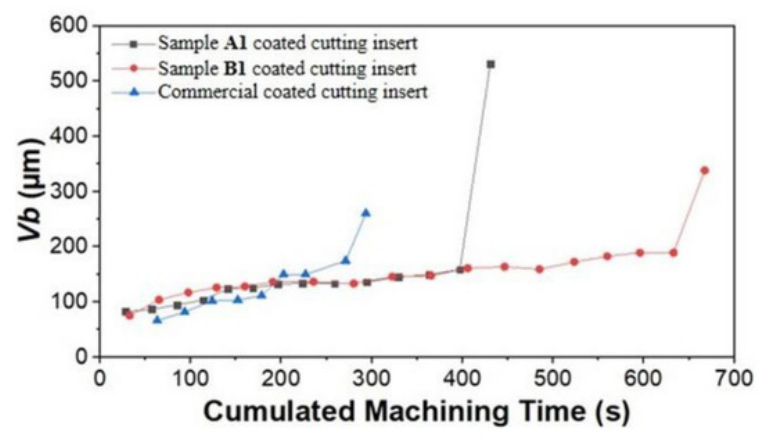
Figure 9.
Tool-life plots for cutting tests of 24CrMoV5-1 steel. Reprinted from ref. [132].
Figure 9.
Tool-life plots for cutting tests of 24CrMoV5-1 steel. Reprinted from ref. [132].
In another study, Chen et al. [133] successfully enhanced the wear resistance of the CVD-coated inserts employing a composite process for CVD post-treatment. In their work, TiN/MT-TiCN/TiN/α-Al2O3 composite coating was deposited on a cemented carbide substrate through CVD and assessed to evaluate the influence of different post-treatment processes. The longest tool life was achieved with the inserts that underwent the combined process.
Apart from ceramic coatings, CVD diamond and related hard carbon allotrope films exhibit extremely high hardness, wear resistance and low coefficient of friction, and are therefore widely used in machining industry for various wear and antiwear tools [134,135]. Synthetic diamond coatings deposited via microwave plasma CVD, exhibit unmatched hardness (90 – 100 GPa) and thermal conductivity (2000 W/m·K). They are used in cutting tools for machining high-strength alloys, extending tool life by 10 to 20 times compared to tungsten carbide [136]. Zhang et al. [137] studied the tribology and cutting performance of boron doped diamond composite coated tool using hot filament CVD technique. Cutting experiments show that boron doped microcrystalline diamond-nanocrystalline diamond film showed excellent wear resistance and the best cutting performance [137]. Zhao et al. [138] demonstrated superior performance of CVD diamond tool when compared with coated cemented carbide tool. In another work, Parray et al. [139] showed that, in contrast to ordinary cemented tungsten carbide (WC-Co) cutting tools, the CVD diamond coatings on WC-Co inserts enhanced machining performance of EN24 steel.
Microelectronics
Among the different deposition techniques for fabricating functional coating systems, CVD has been employed industrially in microelectronics and a large number of other sectors [140,141,142] . CVD is fundamental to semiconductor fabrication, enabling deposition of polysilicon, dielectric films, and metal interconnects with high precision and uniformity. CVD is used for achieving thin films of polycrystalline silicon (poly-Si) or doped poly-Si for use as carrier-selective passivating contacts which are one of the key enabling technologies for the tremendous efficiency improvements in crystalline silicon solar cells [142,143,144,145]. Particularly, APCVD technique enables a low-cost, simple manufacturing process to achieve poly-Si passivating contacts [146]. For integration of transistors in semiconductor industry, metal lines and low-dielectric constant films are used as intermetal dielectrics (IMDs) to reduce RC delays and cross-talk in multilevel metallization process. In this regard, silicon carbon-nitride (SiCN) films or porous low-k SiCOH deposited by PECVD are widely used as a metal diffusion barriers [147,148,149,150].
Superconducting materials
CVD is used to produce high quality coatings of superconductor materials such as MgB2, Nb3Sn with controlled thickness for superior RF performance levels in Superconducting Radio-Frequency (SRF) cavities [151,152,153,154,155].
Superhydrophobic coatings
Transparent, wear-resistant, superhydrophobic inorganic coating on glass substrates are desirable for applications in high building glass curtain, wind shield glass, and solar cell cover glass. Zheng et al. [156] prepared transparent and wear-resistant superhydrophobic film on glass via two-step phase separation and CVD process. Transparent, superhydrophobic polymer nanocone array coatings with excellent mechanical durability and anti-icing performance were fabricated via a facile one-step iCVD process [157].
Besides, ceramic-based superhydrophobic coatings on metal surface provides a protective layer against corrosion [158,159]. For instance, Cao et al. [158] in their study showed better anti-icing performance of the F-SiO2-coated surface as compared to the uncoated surface.
Biomedical coatings
Biomedical coatings are revolutionizing healthcare by enhancing the integration, safety, and functionality of medical devices. These coatings address critical challenges such as infection, biocompatibility, and therapeutic delivery, enabling advancements in implants, prosthetics, and drug delivery systems. Chemically inert passivation layer or antimicrobial coatings on implantable devices not only isolates adjacent channels electrically but also protects the implanted device from the implant-associated infections [160,161,162,163,164,165]. CVD-based coating techniques particularly show distinct advantages for antibacterial application since it allows precise control over coating chemistry and thickness regardless of the substrate characteristics [163,164,165,166]. CVD transforms medical implants by not only adding a high-performance layer that boosts biocompatibility and durability, but also by making surfaces harder and more resistant to wear or corrosion, thereby extending their lifespan [164]. Beyond protection, these coatings can even be engineered to assist with controlled drug delivery directly at the implant site.
Amorphous silicon carbide (a-SiC) coating is widely considered for the biocompatible coating of implantable devices [167]. Su et al. [166] fabricated self-regenerating antibacterial coating surfaces via vapour deposition (iCVD) of layered polymer nanocoatings. The trilayered coating consisted of top and bottom antibacterial PDE layers and an intermediate biodegradable PMAH-based layer, as depicted in Figure 10. Rico et al. [163] deposited graphene on a medical-grade cobalt-chromium alloy surface by RF-PECVD that exhibited high biocompatibility, antibacterial and antifouling properties.
2.3.3. Advantages Challenges and Outlook
CVD offers several key advantages, including excellent coating conformity, high density, strong adhesion, and broad material compatibility. The ability to tailor microstructure through process parameters makes it highly versatile for advanced applications. Recent developments in CVD have focused on reducing processing temperatures, improving precursor efficiency, and enabling environmentally sustainable processes. Plasma-enhanced techniques have significantly expanded the applicability of CVD to temperature-sensitive substrates by lowering reaction temperatures while maintaining film quality. In parallel, advances in precursor chemistry have enabled the controlled growth of nanostructured and functional materials, including graphene, diamond-like carbon (DLC), and other two-dimensional materials, with tailored microstructures and properties.
However, several challenges remain. High processing temperatures in conventional CVD can restrict substrate selection and induce thermal stresses. Additionally, the use of toxic, corrosive, or hazardous precursor gases and the relatively high energy consumption present environmental and safety concerns, while also increasing operational costs posing economic challenges. Achieving uniform deposition over large areas and complex geometries, particularly in industrial-scale systems, remains another critical challenge.
Looking forward, future developments in CVD are expected to focus on low-temperature and energy-efficient processing routes, including further refinement of plasma-assisted and catalytic CVD techniques. The design of safer, more sustainable precursor chemistry will be essential to reduce environmental impact and improve process safety. In addition, integration with hybrid deposition approaches and advanced process control strategies is anticipated to enhance scalability, enabling broader adoption of CVD in next-generation coating technologies across electronics, energy, and structural applications.
2.4. Atomic Layer Deposition (ALD)
Atomic layer deposition (ALD), one of the most sophisticated coating methods, is a vapour-phase thin-film deposition technique based on sequential, self-limiting surface reactions, enabling atomic-scale control over film thickness and composition. In a typical ALD cycle, precursor gases are introduced alternately into the reaction chamber, where each precursor reacts with the substrate surface in a controlled manner, forming a single atomic layer per cycle, offering unprecedented control over film growth at the atomic scale (Figure 11). Excess precursors and reaction by-products are removed through purging steps, ensuring high film uniformity. Due to its unique growth mechanism, ALD is particularly well suited for depositing conformal coatings on complex and high-aspect-ratio structures, making it indispensable in nanoscale applications.
2.4.1. Classification of ALD Techniques
ALD processes can be categorized based on activation method and reactor configuration.
(a) Thermal ALD: It is the most conventional form of ALD and relies purely on thermal energy rather than plasma to activate precursors. It typically operates within a defined ALD temperature window (150-350 ºC), providing excellent conformality over high-aspect-ratio structures and precise control over film thickness, however, is limited to precursors that are sufficiently reactive.
(b) Plasma-enhanced ALD (PEALD): Also known as plasma-assisted ALD, it is a thin-film deposition technique that uses plasma-generated reactive species (such as radicals) rather than thermal energy to grow high-quality, ultra-thin coatings at low temperatures. It is used in semiconductor manufacturing to deposit materials like titanium nitride (TiN), silicon nitride (SiN) and aluminum oxide (Al2O3) on temperature-sensitive substrates, offering improved material density, reduced impurities, and faster process times [176,177,178].
(c) Spatial ALD (SALD): It is an advanced, high-throughput thin-film coating technique where precursor gases are separated physically in space rather than time, allowing for continuous, rapid deposition at atmospheric pressure. Unlike traditional ALD, which is slow due to sequential gas purging, Spatial ALD continuously injects precursors, with inert gas barriers keeping them separate. The process is easily scaled up and compatible with roll-to-roll (R2R) and sheet-to-sheet (S2S) processing, while maintaining the high-quality, pinhole-free, and conformal, atomic-level thickness control of traditional ALD. Spatial ALD is a “game-changer” for industrializing ALD technology, reducing costs and energy consumption while enhancing production efficiency. SALD is used for developing flexible electronics and display technology; coating electrodes, membranes, and separators for lithium-ion batteries and fuel cells (e.g., Al2O3, TiO2, ZnO); applying passivation layers to high-efficiency solar cells and as barrier layers for creating thin films to protect against moisture and oxygen [179].
(d) Area-Selective ALD (AS-ALD): is a bottom-up, thin-film deposition technique that selectively grows material only on designated surface areas rather than the entire substrate. By using inhibitor molecules or inherent surface differences to block deposition elsewhere, it achieves nanoscale thickness control while eliminating complex masking steps, reducing cost and edge placement errors. AS-ALD is crucial in advanced semiconductor manufacturing and nanotechnology, including next-generation nanoelectronics [180] and patterning 2D materials (e.g., selective growth on 2D materials like MoS2 or graphene) [181].
(e) Molecular Layer Deposition (MLD): It is a variant of ALD that uses sequential, self-limiting surface reactions to deposit organic or organic-inorganic hybrid materials at the molecular level, producing polymer-like thin films and hybrid coatings with subnanoscale precision. MLD is often used for flexible coatings, battery electrodes, biomedical devices, and barrier layers [182,183].
Among these variants, thermal ALD remains dominant for high-quality films, while plasma-enhanced and spatial ALD are increasingly adopted to overcome limitations related to temperature and throughput, respectively.
2.4.2. Applications of ALD Coatings
ALD is widely utilized in applications requiring ultrathin, highly uniform coatings, such as:
Microelectronics
ALD has become indispensable in semiconductor device fabrication, enabling deposition of high-ĸ dielectric (such as ZrO2, Al2O3, and HfO2) layers, channel materials, metal gate electrodes, diffusion barriers, and gate oxides [184,185,186,187]. Intel was the first to implement ALD in CMOS circuits with HfO2-based high-к films, replacing traditional thermally grown SiO2 gate dielectrics. Figure 12 shows a SEM image of ALD-deposited SiO2 film having a conformality of >95% [188].
Recently, Liu et al. [189] successfully fabricated high-performance ZnO thin-film transistors at few μm-resolution using low temperature-ALD (at 150 ºC), patterned by high-resolution reverse-offset printing (Figure 13). Highly conductive ultrathin niobium carbide thin films (2.6 nm) as diffusion barriers for Cu and Ru interconnects were grown by PE-ALD on SiO2 substrates at 100–400 °C [190]. Figure 14 (a-b) shows the four-point bending test performance of the PEALD-NbCx coatings as adhesion promoting layer for Cu and Ru interconnects, showing high critical loads and scratch resistance in the mechanical tests [190]. Figure 14c shows the uniform and conformal coating of NbCx film onto the complex topography of the 3D trench, with a step coverage of ~100% achieved using PE-ALD [190]. Development of flexible wearable electronics has also benefited through advances in ALD nano-coating [191,192,193]. Li et al. [191] fabricated high-performance flexible field-effect transistors based on ferroelectric Zr-doped HfO2 (HZO) and ultrathin ITO channels on a flexible MICA substrate (Figure 15), where 100 nm Al2O3 and 11.4 nm HZO was grown by ALD at 250 °C.
Energy conversion and storage applications
ALD coatings improve the stability and performance of lithium-ion batteries, supercapacitors, and perovskite solar cells by enhancing interfacial stability and preventing degradation. In solar cells (including silicon, organic, thin film, perovskite, and quantum dot cells), ALD coatings are used as a surface passivation layer, buffer layer, window layer, absorber layer, electron/hole contact or transparent conductive oxide [143,194,195,196,197,198,199,200,201]. For example, research has shown that ALD facilitates controllable ultra-thin and dense surface coating of quantum dots (QDs) at the atomic scale, enabling stability and longevity of their exceptional optoelectronic performance, indispensable for QD-based devices such as QLEDs, solar cells, microLED displays [202,203,204,205]. Cheng et al. [203] reported on photo-stability enhancement of Al2O3-passivated colloidal CdSe/ZnS QDs. Selective surface passivation via ALD protects QDs from photo-oxidation and enhances photo-stability, critical for LED applications. Xie et al. [202] coated TiO2 nanorod arrays/CdS quantum dots via ALD, enhancing their photoelectrochemical and photocatalytic performance.
Leveraging conformal coatings and pin-hole-free films with atomic-level thickness, ALD has shown great potential in deposition and surface modification of advanced electrode materials in electrochemical energy storage devices [202,206,207,208,209,210,211,212,213,214]. For example, Lopa et al. [214] fabricated ALD-deposited tungsten trioxide/molybdenum trioxide (WO3/MoO3) nanohybrid heterostructure electrodes, achieving high energy storage capacity and stability.
Protective and barrier coatings
Thin ALD layers serve as membranes/barrier films that are used for filtration of water and air, and also act as effective moisture and gas barriers in flexible electronics and packaging applications [215,216,217,218,219,220]. For instance, Yang et al. [220] prepared protein-activated ALD-TiO2-coated membrane, resulting in superhydrophilic nanoarmour on the membrane that demonstrated robust wettability and crude-oil-repellent stability.
Catalyst Surface Engineering
ALD enables atomic-scale surface engineering of catalysts and nanostructured materials with exceptional control over thickness, composition, and conformality. For designing efficient and durable catalysts, ALD has shown unique merits by allowing precise tuning of active sites and surface chemistry through the deposition of highly dispersed nanoparticles or even single atoms, and ultrathin overcoats, thereby tailoring the support-catalyst interface for enhancing electrochemical performance [221,222,223,224,225,226]. Currently, the molecular- and plasma enhanced-ALD techniques are widely used for the development of advanced catalysts [226]. Song et al. [227] presented a pioneering work on creating a sub-nano WO3 bridge layer between Pt nanoparticles and carbon substrate (nitrogen-doped carbon nanotubes, NCNT) through ALD, resulting in Pt-WO3-NCNT catalyst exhibiting remarkable stability and catalytic activity. Chen et al. [223] prepared highly efficient and stable Pt-MoO3/CNT electrocatalyst via ALD for methanol oxidation and oxygen reduction reaction.
2.4.3. Advantages Challenges and Outlook
ALD offers several distinct advantages over conventional deposition techniques, including
atomic-scale thickness control (film thickness can be precisely tuned by controlling the number of deposition cycles), excellent conformality (uniform coatings can be achieved on complex geometries, porous materials, and high-aspect-ratio structures), high film quality (dense, pinhole-free films with excellent uniformity and reproducibility) and low-temperature processing (compared to conventional CVD, ALD can operate at relatively lower temperatures, enabling deposition on temperature-sensitive substrates). Recent developments in ALD have focused on improving scalability and expanding its applicability. Spatial ALD has emerged as a promising approach to increase deposition rates by eliminating purge steps, thereby enabling continuous processing. In addition, roll-to-roll ALD systems have been developed for large-area and flexible substrates, facilitating applications in flexible electronics and advanced coatings. Another significant advancement is area-selective ALD, which enables deposition on predefined surface regions without the need for conventional lithography, making it highly attractive for next-generation nanofabrication and device integration.
Despite its advantages, several challenges limit the widespread industrial adoption of ALD. The inherently slow growth rate associated with cyclic, self-limiting reactions restricts throughput, particularly for thick coatings or large-scale production. Furthermore, the availability of suitable precursors remains constrained by requirements such as volatility, thermal stability, and reactivity, which can limit material versatility and increase process cost.
Moreover, the precise timing and control of precursor exposure and purging steps increase system complexity of the ALD process.
Looking forward, ongoing research is directed toward overcoming these limitations through the development of high-throughput ALD techniques, such as spatial and plasma-enhanced variants, as well as the design of novel precursor chemistries. In addition, hybrid deposition strategies that combine ALD with techniques such as PVD or CVD are expected to play a crucial role in balancing precision, conformality, and scalability. These advancements are anticipated to expand the application of ALD in emerging fields including energy storage, nanoelectronics, and multifunctional coatings.
ALD-based monolithic three-dimensional architecture provides a promising platform for next-generation electronic systems, integrating enhanced functional diversity (preserving the performance of two-dimensional devices) and higher integration density (along the vertical dimension). Application fields include neuromorphic hardware, integrated photonic circuits, and flexible electronic devices [175].
2.5. Electrodeposition
Electrodeposition is a versatile electrochemical technique used to deposit metallic, alloy, and composite coatings from electrolyte solutions onto conductive substrates [228]. The process is typically based on the reduction of metal ions at the cathode under an applied potential (or current), enabling control over coating thickness, composition, and microstructure [229]. According to IUPAC, electrodeposition is the deposition of dissolved or suspended species onto an electrode under an applied electric field, a broad definition that encompasses processes such as electrophoretic deposition, electropainting, and both anodic and cathodic electrodeposition. In many coating studies, however, “electrodeposition” is used more narrowly to mean cathodic metal deposition (“electroplating”), where a metallic film forms on a substrate through electrochemical reduction of metal ions from the electrolyte; the deposited amount is governed by the charge passed [230].
One of the key advantages of electrodeposition is its ability to produce nanostructured and composite coatings through controlled manipulation of deposition parameters such as current density, electrolyte composition, and bath temperature. Techniques such as pulse and pulse-reverse electrodeposition have been extensively developed to refine grain size, enhance coating density, and improve functional performance. The method’s low energy consumption and near-ambient processing conditions make it environmentally favorable; however, achieving uniform coatings on complex geometries often requires careful control of electrodeposition parameters including bath chemistry and agitation/mass transport conditions [231,232,233,234,235,236,237,238,239].
2.5.1. Classification of Electrodeposition Techniques
Electrodeposition techniques can be broadly classified based on the nature of the charged species involved, the deposition mechanism, and modifications to the electrochemical process used to tailor coating properties.
a) Cationic Electrodeposition (CED) and Anionic Electrodeposition (AED): Based on the charge of the depositing species, electrodeposition is commonly divided into cationic electrodeposition (CED) and anionic electrodeposition (AED). In CED, positively charged species migrate toward the cathode and are deposited as a coating, whereas in AED, negatively charged species move toward the anode [240,241]. Cathodic electrodeposition (CED) is an important advance in coating technology, developed to overcome key limitations of conventional methods. It enables rapid formation of highly uniform films with strong corrosion resistance, broad and consistent coverage (including complex geometries), and low material waste. The use of waterborne resins further improves the process by reducing or eliminating VOC emissions, lowering cost, and improving environmental performance.
Compared with traditional solvent-based coating approaches, CED relies primarily on water-based resin systems such as acrylic, epoxy, epoxy–acrylate, and polyurethane. The process requires specially engineered resins that can be rendered electrophoretically mobile and deposited onto cathodic substrates. As a result, CED coatings typically deliver improved corrosion protection, strong adhesion to metals, and effective coverage of irregular surfaces and intricate designs. Despite these advantages, relatively few reviews comprehensively address CED process parameters, recent developments, and strategies for tailoring resins for CED applications.
These techniques are widely used in industrial coating processes, particularly for corrosion protection in automotive and structural applications due to their ability to provide uniform and adherent films.
b) Electrophoretic Deposition (EPD): A closely related but distinct technique is electrophoretic deposition (EPD), which involves the movement and deposition of charged particles, often non-conductive materials such as ceramics or polymers, under an applied electric field [242]. Unlike conventional electrodeposition, EPD enables the fabrication of coatings from suspensions of colloidal particles and is particularly suitable for producing uniform coatings on complex geometries.Because particles generally retain their charge after deposition, layer control depends strongly on using compatible, similarly charged powders and appropriate solvent–binder–dispersant systems. EPD is increasingly applied beyond traditional wear-resistant and anti-oxidant coatings, including functional films for microelectronics and solid oxide fuel cells, bioactive coatings for implants, nanoscale assembly, complex compounds, and ceramic laminates [243,244,245,246,247,248]. Its main intrinsic limitation is that water is typically unsuitable due to gas evolution at the electrodes, but this is mitigated by the availability of many non-aqueous solvents.
c) Specialized Electrodeposition Variants
In addition to these fundamental classifications, several advanced and modified electrodeposition techniques have been developed to enhance coating performance and functionality. Some of them are outlined below.
Pulse Electrodeposition (PED): employs pulsed or pulse-reverse current instead of continuous direct current, enabling improved control over nucleation and growth processes, resulting in refined grain structures and enhanced mechanical and corrosion-resistant properties [249,250].
Composite Electrodeposition: Involves the co-deposition of solid particles, such as Al2O3, SiC, or carbon-based nanomaterials, within a metallic matrix to produce coatings with superior hardness, wear resistance, or self-lubricating characteristics.
Electrophoretic co-deposition: Extends the EPD approach by enabling the simultaneous incorporation of multiple material phases, such as ceramic nanoparticles and carbon nanotubes, to form multifunctional nanostructured coatings, frequently used in functional applications like fuel cell components.
Brush Electrodeposition: A localized variant used for repair and selective coating, where the electrolyte is applied via a moving electrode brush, allowing precise material deposition on targeted regions. Brush electrodeposition methods allow localized repair or enhancement of worn or damaged surfaces without the need for full-scale re-coating.
Autodeposition: A chemically driven coating process that does not require an external power supply. Instead, film formation occurs through a self-limiting redox reaction at the substrate surface. Although distinct from conventional electrodeposition, it is often discussed within this broader category due to its similar applications in corrosion protection and surface finishing.
Ultrasound-assisted electrodeposition (UAED): UAED has gained attention as a practical route to improve the quality and performance of electrodeposited metallic coatings compared with conventional depositions. Recent work shows that applying ultrasound can influence deposit morphology, crystal growth, and the resulting mechanical properties. These effects are commonly attributed to enhanced mass transport arising from cavitation, acoustic streaming (microflow), and acoustic pressure fluctuations, which reduce concentration polarization and promote more uniform ion supply at the electrode surface. As a result, UAED often produces finer-grained deposits with smoother surfaces, higher density, and fewer defects, translating into improved hardness and, in many cases, better wear and corrosion resistance.
Despite these benefits, several barriers still limit broad industrial uptake, including scale-up constraints, added energy demand, and potential electrolyte instability under prolonged sonication. Future studies should therefore prioritize optimization of ultrasound conditions (e.g., power, frequency, duty cycle, and transducer configuration), integration with advanced waveforms or hybrid deposition routes, and system-specific process design tailored to the coating material and application. Overall, UAED remains promising for energy, environmental, and high-performance coating applications by addressing deposit non-uniformity issues associated with concentration polarization in traditional electrodeposition.
2.5.2. Applications of Electrodeposition
Electrodeposition is one of the most frequently used methods for preparing thin metal films and applying metal or polymer coatings to conductive surfaces and is widely employed in applications ranging from corrosion protection and decorative coatings to energy systems and microelectronics. Common applications include:
Corrosion protection and wear-resistance
Electrodeposited coatings such as nickel, zinc, and chromium provide uniform, adherent layers that protect metal substrates from oxidation and corrosion in marine, automotive and tribological applications. Nanocomposite coatings (e.g., Ni-P-SiC, Ni-B-TiN, Ni-CeO2, Ni-Co-Al2O3) enhance hardness and reduce friction, extending the service life of mechanical components, gears, and cutting tools [251]. Besides a broad spectrum of coating materials, including chromium, nickel, cobalt, zinc and copper, alloying elements to a single metal coating can result in better in-service performance, achieving enhanced mechanical, tribological and corrosion protection. Extensive work has been done to investigate the influence of co-deposition of nanoparticles (e.g., SiC, CNTs, Al2O3), electrodeposition conditions and parameters on mechanical, tribological, wear and corrosion performance [252,253,254,255,256,257,258,259,260,261,262,263,264,265].
Decorative finishing
Electrodeposition enables highly uniform and aesthetically appealing finishes for consumer products, jewellery, and architectural metals, while simultaneously providing corrosion protection and mechanical durability [266,267,268,269,270,271]. Electrodeposition for decorative applications provides a lustrous, durable finish on metal and plastic substrates, enhancing aesthetic appeal and corrosion resistance for jewellery, automotive trim, and household fixtures. Common materials include gold, silver, nickel, copper, brass, and chromium alternatives (tin-cobalt).
For copper, industry has traditionally used alkaline cyanide baths, valued for good coverage and controllability, but these are increasingly replaced because of toxicity, disposal burden, and relatively low efficiency and brightness [272]. Lower-impact alternatives such as pyrophosphate electrolytes exist, though they are less stable and more condition-sensitive [273]. Acid copper sulfate–sulfuric baths are now dominant in many applications because they are simple, inexpensive, highly conductive, and can produce bright, levelling deposits at high current efficiency [274]. Nickel plating is still common for bright finishes and as a functional intermediate layer, but its use, especially in items that contact skin, has been constrained by health regulations, driving “nickel-free” and low-release (“hypoallergenic”) approaches and accelerating interest in substitutes. In that context, bronze and palladium coatings have grown in importance as barrier and decorative layers, though some established bath families rely on strongly alkaline, cyanide-containing chemistries that require tight control. Gold plating remains central where high corrosion resistance, conductivity, and appearance are needed. Beyond these, silver, rhodium, platinum, ruthenium, and chromium are used for specific combinations of reflectivity, hardness, inertness, or wear resistance, with a broader trend away from the most hazardous electrolytes (notably cyanides and hexavalent chromium) toward more compliant alternatives.
Modern techniques, such as pulsed current electrodeposition, improve brightness, uniformity, gloss, and deposition efficiency. For instance, Mariani et al. [275] demonstrated that Au-Ni deposits obtained by pulsed currents had finer and compact grains, leading to smoother, glossier, brighter finish and markedly improved corrosion resistance than the deposits obtained using direct current. In another work, Mariani et al. [276] presented a systematic study of pulse and pulse reverse plating on acid copper bath for decorative and functional applications, and concluded that pulsed current show improved characteristics compared to those obtained with direct current, while reverse pulsed currents are preferable for applications where homogeneity of metal thickness is favored over aesthetics. Verrucchi et al. [269] reported on electrodeposition of Sn-Ru Alloys by employing direct, pulsed, and pulsed reverse current for decorative applications. The uniformity of the electrodeposited layer was analyzed by XRF (Figure 16). The sample deposited using pulsed reverse current (tC = 2 ms) showed a remarkably homogeneous thickness with a standard deviation of 2 nm.
Functional surfaces
Electrodeposited catalysts, including cobalt-phosphide or nickel-iron alloys, are used for hydrogen and oxygen evolution reactions in electrocatalysis, as well as for battery electrodes. Additionally, electrodeposited electrodes are employed in water purification, fuel cells, and energy storage devices. In the field of energy, electrodeposited materials such as cobalt phosphide on conductive substrates have demonstrated excellent electrocatalytic activity for hydrogen evolution reactions, highlighting the technique’s relevance in sustainable energy technologies. Jia et al. [240] successfully deposited two-dimensional conductive metal-organic framework on nickel foam for use as electrodes for supercapacitors that demonstrated outstanding performance.
Besides corrosion and wear resistance, the electrodeposited Ni-Fe coating is largely employed for magnetic (such as pole pieces in magnetic valves, magnetic heads for tape recorders, flux guides in thin film write heads and shields for magnetic recording or the cores of on-chip inductors etc) and electronic applications (e.g., memory, recording and storage devices in computers, Null-balance transformer, pulse transformers, relay parts etc.) [277,278,279,280,281,282]. Rasmussen et al. [278] developed a new bath formulation for pulse reverse electroplating of CoNiFe for their magnetic microsystems’ applications. Sun et al. [281] electrodeposited Ni80Fe20 Permalloy for use as the magnetic core to increase the inductance and quality factor of integrated flexible parylene-based MEMS inductors. In another work, a giant magnetoresistance ratio of 5.4% was achieved for electrodeposited [Ni80Fe20/Cu/Co/Cu] spin-valve multilayers on NiFe buffer layers [280].
Electronics and Microfabrication
The technique is widely used to fabricate metallic interconnects, conductive traces, and microstructures for printed circuit boards (PCBs), microelectronic devices, and MEMS components, benefiting from precise thickness control and high reproducibility [283,284,285,286,287]. In this context, electrodeposited nano-twinned metals have been studied extensively for applications in interconnects in nanoelectronic devices and nanoelectromechanical systems owing to their excellent strength, ductility, and electrical conductivity [285]. Nanoscale twin metal formation has been achieved by both direct current and pulsed current deposition [288,289,290,291,292,293,294,295,296,297,298]. For example, Dong et al. [297] reported nanotwinned Cu micro-cone arrays fabricated by pulse electrodeposition without any template. It was observed that the morphologies of the micro-cones were controllable by Cl- concentration in the electrolyte. Also, it was realized that the nanotwinned micro-cone array enabled the low-temperature bonding a 50% enhancement, rendering it promising for advanced 3D electronic packaging applications.
Metal-recovery
Electrodeposition is widely used in hydrometallurgy, particularly in the fields of metal recovery. Examples include the extraction of precious metals, such as gold, silver, and copper, from solution by means of electrodeposition or electrochemistry-based metal recovery [299,300,301,302,303]. Li et al. [300] recovered nickel from real electroplating wastewater using a cost-effective manner by integrating electrodeposition with adsorption pretreatment technique. Wang et al. [303] performed stepwise recovery of gold and silver from E-waste via stepwise electrodeposition. In another work, Li et al. [302] employed flotation-assisted electrodeposition process to recover copper from waste printed circuit boards.
Biomedical Coatings
Electrodeposition of biocompatible materials such as hydroxyapatite (HAp) or calcium phosphate on implants improves osseointegration, corrosion resistance, and overall biocompatibility in physiological environments [304,305]. Chitosan-based coatings modified with gold or zinc nanoparticles are considered effective strategy to prevent bacterial infections in implants [306,307]. Among the wet methods, the various electrodeposition approaches for chitosan, HAp and reinforced HAp nanocomposite (such as HAp-CNTs, HAp-GO, HAp-Chitosan, HAp-TiO2) coatings include direct/pulse electrodeposition, electroless and electrophoretic deposition [304,305,308,309,310,311,312,313,314].
Coatings on titanium and titanium alloy (such as Ti6Al4V, NiTi) are favored for implants due to their outstanding biocompatibility and osseointegration, low density, resistance to corrosion, and high mechanical strength [315,316,317,318,319,320,321,322,323,324,325]. Besides, Zn-, Mg-based alloys, Co-Cr alloys and 316 L stainless steels are also used in load-bearing implant applications [326,327,328,329,330,331,332,333].
For example, electrodeposition of HAp-TiO2 composite coating improved the corrosion resistance of NiTi by almost 50% [316], while, pulsed electrodeposition of HAp-Ta2O5 composite coatings on NiTi improved the corrosion resistance and decreased the Ni ion release of the samples up to 205 % and 91 %, respectively [324]. In a recent work, Souri et al. [334] reported on electrochemical deposition of homogeneous HAp-Ag nanostructured coating which enhanced the antibacterial and corrosion resistance of Ti6Al4V alloy.
2.5.3. Advantages, Challenges and Outlook
Electrodeposition offers several compelling advantages that make it a versatile and widely used surface engineering technique. Its electrochemical nature allows precise control over coating thickness, composition, and microstructure by adjusting parameters such as current density, bath composition, temperature, and deposition time. This enables the fabrication of uniform and adherent coatings even on substrates with moderate geometric complexity. In comparison to other deposition techniques, such as PVD or CVD, electrodepositions offer some advantages in terms of simplicity of the process and the low cost of the equipment. While CVD achieves uniform deposition over a large-area, it often requires high temperature and high pressure, consuming high energy, and may also produce harmful byproducts. Likewise, even though PVD prepares high-quality films, the complexity of the process, slow deposition rate and expensive equipment are its downside.
The process is also inherently energy-efficient, as it operates at ambient or mild temperatures, and is scalable for both small components and large industrial surfaces. Moreover, advanced variants such as pulse electrodeposition and composite co-deposition allow the creation of nanostructured or multifunctional coatings, enhancing properties like hardness, corrosion resistance, wear resistance, and catalytic activity. Electrodeposition also accommodates a wide range of metals, alloys, and particle-reinforced composites, including environmentally friendly coatings, further broadening its applicability across industries such as automotive, aerospace, marine, electronics, and energy storage. Deep eutectic solvents have gained attention as non-aqueous electrolyte media for metal electrodeposition. Their appeal stems from a combination of properties often aligned with greener processing, including low volatility, good thermal stability, relatively low toxicity, biodegradability, and low cost [335].
Despite these advantages, electrodeposition presents several limitations that must be addressed for optimal performance. Achieving uniform deposition on highly complex or recessed geometries remains challenging due to variations in local current density and mass transport limitations. Coatings may develop internal stresses or defects such as porosity, cracks, or nodules, which can compromise mechanical integrity and long-term durability. The choice of electrolyte, additives, and particle dispersions critically affects coating quality. Furthermore, the use of certain electrolytes and additives pose environmental or safety concerns, necessitating the development of greener and more sustainable bath chemistries.
Additionally, while pulse and composite techniques improve performance, they often involve more complex setups, longer processing times, or increased operational costs, limiting high-throughput industrial adoption in some cases. Careful optimization of process parameters and bath formulations is therefore essential to balance performance, reproducibility, and sustainability in electrodeposition-based coatings.
Recent advances in electrodeposition have focused on enhancing coating performance, uniformity, and functional versatility through improved process control and electrolyte engineering. Techniques such as pulse and pulse-reverse electrodeposition have enabled the fabrication of fine-grained and nanostructured coatings with superior mechanical properties, corrosion resistance, and adhesion. The incorporation of nanoparticles into the plating bath has further facilitated the development of metal–matrix composite coatings with tailored functionalities, including enhanced wear resistance, catalytic activity, and multifunctionality. Emerging strategies, such as electrodeposition under magnetic or ultrasonic fields, have improved mass transport and coating uniformity, addressing limitations associated with complex geometries and substrate accessibility.
Looking forward, research is expected to focus on the development of environmentally benign electrolytes, optimized bath chemistries, and advanced real-time monitoring techniques to improve deposition control and reproducibility. The integration of electrodeposition with complementary surface engineering methods and additive manufacturing approaches is likely to enable multifunctional and hybrid coatings with enhanced mechanical, chemical, and functional performance. These developments position electrodeposition as a key technology for emerging applications in energy storage, catalysis, advanced electronics, and biomedical devices, highlighting its continued relevance in next-generation surface engineering.
3. Conclusions and Future Perspectives
Surface coating technologies have become indispensable in modern manufacturing and materials engineering, offering effective routes to enhance durability, functionality, surface protection, and overall component performance. This review has highlighted the major coating approaches, including physical techniques such as PVD, CVD, as well as chemical methods such as ALD, and electrodeposition. Together, these technologies provide control over the coating thickness, composition, structure, adhesion, and surface functionality, enabling their use across a wide range of industrial sectors.
The evolution of coatings is marked by the convergence of advanced deposition techniques, novel materials, and intelligent design, enabling multifunctional systems that address sustainability and performance. Combining PVD, CVD, and ALD allows manufacturers to engineer materials from the atomic scale up to the macro scale. This hybrid approach, often called sequential or synergistic deposition, allows engineers to exploit the unique strengths of each method while mitigating their individual limitations. For instance, by using ALD for precision interfaces, CVD for high-quality bulk materials, and PVD for dense metallic finishes, industries can create faster microchips, longer-lasting tools, and next-generation energy devices that would not be possible using any single method alone. Recent progress has been driven by advances in materials design, process optimization, and digital tools. The integration of artificial intelligence is particularly important, as it can support parameter optimization, defect prediction, process adjustments in real-time monitoring, and faster development of coating systems with improved reliability and reproducibility. At the same time, emerging concepts such as self-healing coatings, biomimetic surfaces, smart responsive coatings, and hybrid deposition processes are expanding the functional scope of coated materials.
Sustainability will be a decisive factor in the future development of coating technologies. Many conventional processes still involve high energy consumption, hazardous chemicals, solvent use, or volatile organic compound emissions. Consequently, greener approaches such as low-temperature deposition, water-based sol-gel processing, solvent-free formulations, recyclable materials, and bio-based coatings should receive greater attention. Life cycle assessment can guide the selection of materials and processes with lower environmental impact, reduced waste, and improved resource efficiency. Aligning coating technologies with circular economy principles will be essential for achieving both high performance and environmental responsibility.
Overall, surface coating technologies are expected to remain a key driver of innovation in materials science and industrial engineering. Their future development will depend on the integration of advanced materials, precise processing, AI-driven optimization, multifunctional design, and sustainable manufacturing. By addressing current challenges related to scalability, durability, cost, and environmental impact, surface coatings can continue to support safer, cleaner, and more efficient technologies across diverse application areas.
Acknowledgments
The author I.C. would like to acknowledge funding from “Agenda DRIVOLUTION – Transition to the factory of the future” project supported by the PRR - Recovery and Resilience Plan and by NextGenerationEU, through the scheme Capitalisation and Business Innovation (Ref: 02-C05-i01.02-2022.PC644913740-00000022). I. Coondoo would also like to acknowledge financial assistance by national funds provided by FCT – Fundação para a Ciência e a Tecnologia, I.P., through individual FCT-CEEC Assistant Researcher contract (2024.09019.CEECIND). The authors acknowledge funding from Project “SINT3R” (ref: COMPETE2030-FEDER-02219100). This work was partly developed within the scope of the project CICECO Aveiro Institute of Materials, UID/50011/2025 (DOI 10.54499/UID/50011/2025) & LA/P/0006/2020 (DOI 10.54499/LA/P/0006/2020), financed by national funds through the FCT/MCTES (PIDDAC).
References
- Sun, H.; et al. Recent Representative Progress of Surface Coating Technology. Chem. Rec. 2025, 25(8), e202500054. [Google Scholar] [CrossRef] [PubMed]
- Butt, M.A. Thin-Film Coating Methods: A Successful Marriage of High-Quality and Cost-Effectiveness—A Brief Exploration. Coatings 2022, 12, 1115. [Google Scholar] [CrossRef]
- Kumar, A.; et al. Modern Coating Processes and Technologies, in Coating Materials: Computational Aspects, Applications and Challenges; Verma, A., Sethi, S.K., Ogata, S., Eds.; Springer Nature Singapore: Singapore, 2023; pp. 33–80. [Google Scholar]
- Baptista, A.; et al. Sputtering Physical Vapour Deposition (PVD) Coatings: A Critical Review on Process Improvement and Market Trend Demands. Coatings 2018, 8, 402. [Google Scholar] [CrossRef]
- Fox, V.; et al. Hard lubricating coatings for cutting and forming tools and mechanical components. Surf. Coat. Technol. 2000, 125(1), 347–353. [Google Scholar] [CrossRef]
- Patro, S.S.; Sahoo, A.K.; Roy, S. Analysis of residual stresses in cutting tools coated via physical vapour deposition: A review. Mater. Today Proc. 2023. [Google Scholar] [CrossRef]
- PalDey, S.; Deevi, S.C. Single layer and multilayer wear resistant coatings of (Ti,Al)N: a review. Mater. Sci. Eng. A 2003, 342(1), 58–79. [Google Scholar] [CrossRef]
- Ariharan, N.; et al. A comprehensive review of vapour deposited coatings for cutting tools: properties and recent advances. Trans. IMF 2022, 100(5), 262–275. [Google Scholar] [CrossRef]
- Liu, Y.; et al. Multilayer Coatings for Tribology: A Mini Review. Nanomaterials 2022, 12, 1388. [Google Scholar] [CrossRef] [PubMed]
- Xin, T.; Pei, H.; Shucai, Y. Coating and micro-texture techniques for cutting tools. J. Mater. Sci. 2022, 57(36), 17052–17104. [Google Scholar] [CrossRef]
- Okokpujie, I.P.; et al. Effect of Coatings on Mechanical, Corrosion and Tribological Properties of Industrial Materials: A Comprehensive Review. J. Bio-Tribo-Corros. 2023, 10(1), 2. [Google Scholar] [CrossRef]
- Shakib, S.E.; Babakhani, A.; Torbati, M. Kashefi. Nanomechanical assessment of tribological behavior of TiN/TiCN multi-layer hard coatings deposited by physical vapor deposition. J. Mater. Res. Technol. 2023, 25, 1344–1354. [Google Scholar] [CrossRef]
- Muhammed, M.; et al. A Comprehensive Review of Cathodic Arc Evaporation Physical Vapour Deposition (CAE-PVD) Coatings for Enhanced Tribological Performance. Coatings 2024, 14, 246. [Google Scholar] [CrossRef]
- Kaya, E. Physical Vapor Deposition of Thin Film Coatings for Cutting Tools, in Micromanufacturing Operations; Gürgen, S., Ed.; Springer Nature Switzerland: Cham, 2026; pp. 133–154. [Google Scholar]
- Zhou, M.; et al. Phase transition and properties of Ti–Al–N thin films prepared by r.f.-plasma assisted magnetron sputtering. Thin Solid Films 1999, 339(1), 203–208. [Google Scholar] [CrossRef]
- Kimura, A.; et al. Metastable Ti1−xAlxN films with different Al content. J. Mater. Sci. Lett. 2000, 19(7), 601–602. [Google Scholar] [CrossRef]
- Musil, J.; Hrubý, H. Superhard nanocomposite Ti1−xAlxN films prepared by magnetron sputtering. Thin Solid Films 2000, 365(1), 104–109. [Google Scholar] [CrossRef]
- Schäffer, E.; Kleer, G. Mechanical behavior of (Ti,Al)N coatings exposed to elevated temperatures and an oxidative environment. Surface and Coatings Technology 2000, 133-134, 215–219. [Google Scholar]
- Wu, S.K.; Lin, H.C.; Liu, P.L. An investigation of unbalanced-magnetron sputtered TiAlN films on SKH51 high-speed steel. Surf. Coat. Technol. 2000, 124(2), 97–103. [Google Scholar] [CrossRef]
- Kimura, A.; et al. Hot-pressed Ti-Al targets for synthesizing Ti1−xAlxN films by the arc ion plating method. Thin Solid Films 2001, 382(1), 101–105. [Google Scholar] [CrossRef]
- Shugurov, A.R.; Kuzminov, E.D. Mechanical and tribological properties of Ti-Al-Ta-N/TiAl and Ti-Al-Ta-N/Ta multilayer coatings deposited by DC magnetron sputtering. Surf. Coat. Technol. 2022, 441, 128582. [Google Scholar] [CrossRef]
- Panjan, P.; et al. Comparative Study of Tribological Behavior of TiN Hard Coatings Deposited by Various PVD Deposition Techniques. Coatings 2022, 12, 294. [Google Scholar] [CrossRef]
- Amirhossein, M.; et al. Enhancing Wear Behavior and Hardness of D5 Cold Work Tool Steel through TiCrN Multilayer Nanocoating via Physical Vapor Deposition. Surf. Eng. Appl. Electrochem. 2024, 60(1), 58–68. [Google Scholar] [CrossRef]
- Guimaraes, M.C.R.; et al. On the effect of substrate oscillation on CrN coatings deposited by HiPIMS and dcMS. Surf. Coat. Technol. 2018, 340, 112–120. [Google Scholar] [CrossRef]
- Li, Q.; et al. The superior properties of CrN coatings prepared by high power pulsed reactive magnetron sputtering. AIP Adv. 2020, 10(1), 015125. [Google Scholar] [CrossRef]
- Codau, T.-C.; et al. Advanced ceramic multilayer coatings for increasing the tool life of cutting inserts: A hybrid CVD-PVD approach. Mater. Chem. Phys. 2026, 349, 131768. [Google Scholar] [CrossRef]
- Kumar, S.; Kumar, M. Tribological and Mechanical Performance of Coatings on Piston to Avoid Failure—A Review. J. Fail. Anal. Prev. 2022, 22(4), 1346–1369. [Google Scholar] [CrossRef]
- Liu, J.; Zhang, Y.; Liao, B. A review on preparation process and tribological performance of coatings for internal combustion engine piston ring. Adv. Mech. Eng. 2023, 15(5), 16878132231175752. [Google Scholar] [CrossRef]
- Singh, H.; et al. A Comprehensive Review of Tribological Performance of Coatings on Automotive Piston Rings. I-Manag. J. Mech. Eng. 2024, 14(4), 16. [Google Scholar] [CrossRef]
- Dr. Maria, Z.; Olivia, P.K. Coating Materials for Automotive Piston Rings: A Review of Tribological Performance and Engine Impact. Front. Emerg. Eng. Technol. 2025. 2, 06, 8–15. [Google Scholar]
- Friedrich, C.; et al. PVD CrxN coatings for tribological application on piston rings. Surf. Coat. Technol. 1997, 97(1), 661–668. [Google Scholar] [CrossRef]
- Bobzin, K.; et al. Lubricated PVD CrAlN and WC/C coatings for automotive applications. Surf. Coat. Technol. 2009, 204(6), 1097–1101. [Google Scholar] [CrossRef]
- Lin, J.; et al. Development and evaluation of low friction TiSiCN nanocomposite coatings for piston ring applications. Surf. Coat. Technol. 2016, 298, 121–131. [Google Scholar] [CrossRef]
- Liu, J.; et al. Tribological properties of CrN coating deposited on 20CrMo against tin bronze. Sci. China Technol. Sci. 2018, 61(11), 1713–1722. [Google Scholar]
- Singh, S.K.; et al. Wear behavior of chromium nitride coating in dry condition at lower sliding velocity and load. Int. J. Adv. Manuf. Technol. 2018, 96(5), 1665–1675. [Google Scholar]
- Alisir, S.H.; Evrensel, D. Investigation into Coating Structure and Wear Environment Effects on Tribological Properties of Piston Ring Coated with Monolayer TiAlN and Multilayer TiN/TiAlN. J. Mater. Eng. Perform. 2022, 31(2), 1654–1666. [Google Scholar]
- Singh, H.; Singh, V. Tribological Performance of Coatings on Automotive Piston Rings: A Review. IUP J. Mech. Eng. 2025, 18(1), 47–70. [Google Scholar] [CrossRef]
- Shen, Z.; et al. LaNdZrO thermal barrier coatings by electron beam physical vapor deposition: Morphology, thermal property and failure mechanism. Chem. Eng. J. Adv. 2022, 11, 100328. [Google Scholar] [CrossRef]
- Chen, D.; et al. Hybrid chemical-physical vapor deposition of highly durable environmental barrier coatings. Vacuum 2023, 213, 112098. [Google Scholar] [CrossRef]
- Alhazaa, A.; Shar, M.A. Aerospace and Thin Films, in Thin Films and Coatings: Engineering Applications; Chandio, A.D., Channa, I.A., Eds.; Springer Nature Singapore: Singapore, 2025; pp. 217–238. [Google Scholar]
- Ahanger, Z.A.; Saleem, S.S.; Dey, A. Physical vapour deposition technologies of functionally graded coatings. Proceedings of the Institution of Mechanical Engineers, Part L: Journal of Materials: Design and Applications 2026, 240(3), 472–528. [Google Scholar]
- Ozgurluk, Y.; Karaoglanli, A.C.; Ahlatci, H. Comparison of calcium–magnesium-alumina-silicate (CMAS) resistance behavior of produced with electron beam physical vapor deposition (EB-PVD) method YSZ and Gd2Zr2O7/YSZ thermal barrier coatings systems. Vacuum 2021, 194, 110576. [Google Scholar] [CrossRef]
- Odabas, O.; et al. Investigation of vermiculite infiltration effect on microstructural properties of thermal barrier coatings (TBCs) produced by electron beam physical vapor deposition method (EB-PVD). Surf. Coat. Technol. 2022, 443, 128645. [Google Scholar] [CrossRef]
- Kucharska, B.; et al. Protective Magnetron Sputtering Physical Vapor Deposition Coatings for Space Application. Coatings 2024, 14, 1195. [Google Scholar] [CrossRef]
- Mühlbacher, M.; et al. Copper diffusion into single-crystalline TiN studied by transmission electron microscopy and atom probe tomography. Thin Solid Films 2015, 574, 103–109. [Google Scholar] [CrossRef]
- Mehta, N. Overview of Coating Deposition Techniques, in Tribology and Characterization of Surface Coatings; 2022; pp. 1–32. [Google Scholar]
- Hossain, M.I.; Mansour, S. A critical overview of thin films coating technologies for energy applications. Cogent Eng. 2023, 10(1), 2179467. [Google Scholar] [CrossRef]
- Adeoye, A.E.; Adeaga, O.A.; Ukoba, K. Chemical vapour deposition (CVD) and physical vapour deposition (PVD) techniques: advances in thin film solar cells. Niger. J. Technol. 2024, 43(3), 479–489. [Google Scholar]
- Sharma, G.; et al. Deposition techniques for thin film development in microelectronic devices. AIP Conf. Proc. 2025, 3157(1), 120025. [Google Scholar] [CrossRef]
- Zega, B. Hard decorative coatings by reactive physical vapor deposition: 12 Years of development. In Surface and Coatings Technology; 1989; Volume 39-40, pp. 507–520. [Google Scholar]
- Reiners, G.; Beck, U.; Jehn, H.A. Decorative optical coatings. Thin Solid Films 1994, 253(1), 33–40. [Google Scholar] [CrossRef]
- Constantin, R.; Steinmann, P.-A.; Manasterski, C. Decorative PVD Coatings, in Nanomaterials and Surface Engineering; 2013; pp. 109–162. [Google Scholar]
- Sathish, M.; Radhika, N.; Saleh, B. Current Status, Challenges, and Future Prospects of Thin Film Coating Techniques and Coating Structures. J. Bio-Tribo-Corros. 2023, 9(2), 35. [Google Scholar] [CrossRef]
- van Hove, R.P.; et al. Titanium-Nitride Coating of Orthopaedic Implants: A Review of the Literature. BioMed Res. Int. 2015, 2015(1), 485975. [Google Scholar] [CrossRef] [PubMed]
- Damiati, L.; et al. Impact of surface topography and coating on osteogenesis and bacterial attachment on titanium implants. J. Tissue Eng. 2018, 9, 2041731418790694. [Google Scholar] [CrossRef] [PubMed]
- Sivaprakasam Palani, E.G.M., Melaku Desta, Samson Mekbib Atnaw, Ravi Banoth, Suresh Kolanji, Physical Vapor Deposition Coating Process in Biomedical Applications, in Sustainable Advanced Manufacturing and Materials Processing: Methods and Technologies (1st ed.). S. Kaushal, Singh, I., Singh, S., and Gupta, A, Editor. 2022, CRC Press. p. 244.
- Schaldach, M.; et al. Pacemaker electrodes made of titanium nitride. Biomed. Tech. Eng. 1989, 34(7), 185–190. [Google Scholar] [CrossRef]
- Sin, D.-C.; Kei, H.-L.; Miao, X. Surface coatings for ventricular assist devices. Expert Rev. Med. Devices 2009, 6(1), 51–60. [Google Scholar] [CrossRef] [PubMed]
- Han, W.; et al. Influence of WC particle size on microstructural evolution and wear behavior of laser cladding WC/Ti6Al4V composite coatings. Ceram. Int. 2025, 51(25, Part C), 47119–47131. [Google Scholar] [CrossRef]
- He, R.; et al. Improvement in corrosion and wear resistance of Ni3Al-based superalloy coatings through laser energy density regulation. J. Mater. Res. Technol. 2025. 36, 4585–4601. [Google Scholar] [CrossRef]
- Lei, D.; et al. Microstructure evolution mechanism and microhardness enhancement of (nano-CeO2 + micron TiC)/Ti6Al4V composite coating by laser cladding. Prog. Addit. Manuf. 2025, 10(9), 6643–6655. [Google Scholar] [CrossRef]
- Zhao, C.; et al. Laser Cladding of High-Temperature Alloy: Research Status and Development. Adv. Eng. Mater. 2025, 27(10), 2402956. [Google Scholar] [CrossRef]
- Sow, M.C.; et al. Influence of beam diameter on Laser Powder Bed Fusion (L-PBF) process. Addit. Manuf. 2020, 36, 101532. [Google Scholar] [CrossRef]
- Ren, J.; et al. Strong yet ductile nanolamellar high-entropy alloys by additive manufacturing. Nature 2022, 608(7921), 62–68. [Google Scholar] [CrossRef] [PubMed]
- Zhang, F.; et al. Interfacial microstructure and mechanical properties of 2124 aluminum alloy reinforced by AlCoCrFeNi high entropy alloy. J. Mater. Res. Technol. 2023, 26, 8846–8856. [Google Scholar] [CrossRef]
- Zhao, Q.; et al. Effect of alloying elements (Mn, Ti, and Mo) on the corrosion behavior of FeCoNiCr-based high entropy alloy in supercritical water. Corros. Sci. 2023, 220, 111291. [Google Scholar] [CrossRef]
- Cui, T.; et al. Effect of laser energy density on microstructures and properties of laser cladding CoMoCrSiFe coating. Opt. Laser Technol. 2025, 192, 113529. [Google Scholar] [CrossRef]
- Lei, X.; et al. A hybrid optimization method for determining laser cladding process parameters to control geometric morphology in CoCrFeNiMn high-entropy alloy. J. Mater. Res. Technol. 2025. 39, 1038–1052. [Google Scholar] [CrossRef]
- Liu, H.; et al. Improve wear resistance CoCrFeMnNiTix/WC high entropy alloy-ceramic composite coatings with hybrid ex/in-situ multi-scale reinforcement phase fabricating by laser cladding. Ceram. Int. 2025, 51(23, Part B), 40335–40348. [Google Scholar] [CrossRef]
- Wu, Y.; et al. Tribological behaviour of laser cladding CoCrFeNiMo0.5Tix-hBN high-entropy alloy composite coatings under dry and tribocorrosion conditions. Ceram. Int. 2025, 51(26, Part C), 50396–50418. [Google Scholar] [CrossRef]
- Sexton, L.; et al. Laser cladding of aerospace materials. J. Mater. Process. Technol. 2002, 122(1), 63–68. [Google Scholar] [CrossRef]
- Liu, Q.; et al. Laser cladding as a potential repair technology for damaged aircraft components. Int. J. Struct. Integr. 2011, 2(3), 314–331. [Google Scholar] [CrossRef]
- Chen, M.; et al. Research status of laser cladding technology on aluminum alloy surface. Int. J. Adv. Manuf. Technol. 2025, 137(1), 1–21. [Google Scholar] [CrossRef]
- Lei, J.; et al. Temperature and rate-dependent behavior of laser cladding IN625 alloy under dynamic loading: Experiments and constitutive model. Mater. Today Commun. 2025. 49, 114162. [Google Scholar] [CrossRef]
- Morais, E.C.F.; et al. Laser-induced diffusion of an aluminum clad in an aerospace aluminum alloy for enhanced bonding. Results Surf. Interfaces 2025. 19, 100521. [Google Scholar] [CrossRef]
- Wan, N.; et al. Design and optimization of grinding tool structures for high-performance machining of aerospace difficult-to-cut materials. J. Manuf. Process. 2025. 154, 640–658. [Google Scholar] [CrossRef]
- Xie, F.; et al. Enhanced high-temperature oxidation resistance of TC11 titanium alloys via laser cladding FeCoNiCrMoBSi high-entropy alloy coatings. Mater. Chem. Phys. 2025. 340, 130861. [Google Scholar] [CrossRef]
- Wang, J.; et al. TiNiCuZrNbTa refractory high entropy alloy coatings fabricated using laser cladding: Microstructure and tribological behavior. Tribol. Int. 2026, 214, 111319. [Google Scholar] [CrossRef]
- Zhang, H.; et al. Periodic multilayer functionally graded structure of Ni-NbMoTa high-entropy alloy composition materials via laser cladding deposition. Addit. Manuf. Front. 2026. 5, 1, 200255. [Google Scholar]
- Zhao, C.; et al. Review of the research status and development of laser cladding high-entropy alloys. J. Vac. Sci. Technol. A 2026, 44(2), 020802. [Google Scholar] [CrossRef]
- Liu, C.; et al. Structure and properties of AlCoFeCuMox high entropy alloy coatings prepared by laser cladding and applications on drones for aerospace innovation competitions. J. Alloys Metall. Syst. 2026, 100237. [Google Scholar] [CrossRef]
- Guan, S.; et al. Microstructure Evolution and Mechanical Property Enhancement of 30CrMnSiNi2A Steel Repaired by Laser Cladding with AerMet100 Steel. Met. Mater. Int. 2026, 32(2), 476–489. [Google Scholar]
- Zhao, C.; et al. Microstructure evolution and synergistic strengthening mechanisms of wear and corrosion resistance in laser cladding fabricated TC11-xMo coatings. Tribol. Int. 2026, 214, 111276. [Google Scholar] [CrossRef]
- Natarajan Jeyaprakash, S.S.K., Che-Hua Yang, Repair of Engineering Components through Laser Cladding, in Tailoring of Engineering Material Properties through Laser Cladding: Metallurgical, Mechanical and Tribological Properties, N. Jeyaprakash, Prabu, G., & Yang, C.-H, Editor. 2025, CRC Press. p. 306.
- Wang, Q.-Y.; et al. Tribo-corrosion behavior and mechanism of Ni-WC laser-clad coating in mineralizing solution. J. Mater. Sci. 2025, 60(7), 3408–3429. [Google Scholar] [CrossRef]
- Adefila, E.O.; et al. Failure analysis and remanufacturing techniques in drilling and crushing equipment in mining industries: a review. J. Remanufacturing 2026, 16(1), 6. [Google Scholar] [CrossRef]
- Cui, C.; et al. Design of FeCoNiCrMoX laser cladded coatings for drilling equipment in deep complex environment: Insight into microstructure of reticulated brick-mortar imitated nacre pearl layer. Surf. Coat. Technol. 2026, 521, 133065. [Google Scholar] [CrossRef]
- Zha, E.; et al. Design of process parameters for laser cladded high entropy alloy coatings on deep ground component surface based on machine learning collaborative performance improvement. Mater. Charact. 2026, 234, 116265. [Google Scholar] [CrossRef]
- Karamimoghadam, M.; et al. Laser Surface Transformation Hardening for Automotive Metals: Recent Progress. Metals 2024, 14, 339. [Google Scholar] [CrossRef]
- Wang, K.; et al. Enhancing the Wear Resistance of AlSi9Mg Alloys Using Rotatable Inner-Surface Laser Cladding Method. J. Therm. Spray. Technol. 2025, 34(5), 1747–1762. [Google Scholar] [CrossRef]
- Ying M., S.Y.a.Z.Q. Application analysis of laser cladding technology in the automotive field. in International Conference on Mechanical Manufacturing Technology and Material Engineering. 2025. Springer Nature.
- Li, D.; Zhang, J. Progress in material systems, process control, and performance enhancement of laser cladding technology. J. Adv. Mech. Des. Syst. Manuf. 2026, 20(1), JAMDSM0006–JAMDSM0006. [Google Scholar] [CrossRef]
- Dindar, C.; et al. Tribological and braking performance comparison of martensitic stainless steel coatings deposited by laser cladding and HVOF. [CrossRef] [PubMed]
- Altuncu, E.; et al. Enhanced wear and corrosion resistance of high-speed laser-clad automotive brake discs for Euro-7 compliance. Eng. Res. Express 2025. 7, 3, 035526. [Google Scholar] [CrossRef]
- Ambhore, N.; et al. Laser applications in surface treatment: a comprehensive review. Laser Phys. 2025, 35(10), 106101. [Google Scholar] [CrossRef]
- Zhang, B.; Hua, X.; Yang, F. Study on Wear and Corrosion Resistance of Co-Cr-Ti Composite Coatings on Ti6Al4V by Laser Cladding. JOM 2025, 77(6), 4862–4876. [Google Scholar] [CrossRef]
- Sathish, M.; Radhika, N.; Saleh, B. A critical review on functionally graded coatings: Methods, properties, and challenges. Composites Part B: Engineering. 2021; 225, p. 109278. [Google Scholar]
- Marquardt, R.; Biegler, M.; Rethmeier, M. Functionally graded material for improved wear resistance manufactured by directed energy deposition. Prog. Addit. Manuf. 2025, 10(8), 4973–4978. [Google Scholar]
- Singh, S.; Kumar, C.; Sah, S.K. Review on laser powder-based directed energy deposition for fabricating functionally graded materials: Microstructure, mechanical behavior, and defect analysis. J. Laser Appl. 2025, 37(4), 041202. [Google Scholar] [CrossRef]
- Kopec, M. Functionally Graded Nickel-Based Coatings: A Comprehensive Review. Coatings 2026, 397. [Google Scholar] [CrossRef]
- Wan, S.; et al. A novel laser-cladded AlCuTiVCr/Cu-Al functionally graded coating with excellent corrosion resistance on Mg-Li alloy. Mater. Lett. 2023, 350, 134944. [Google Scholar] [CrossRef]
- Chen, L.; et al. Microstructure and properties of in situ TiC/Ni functionally gradient coatings by powder-fed laser cladding. Ceram. Int. 2022, 48(24), 36789–36801. [Google Scholar] [CrossRef]
- Wang, G.; et al. Synthesis of Ni-WC/Al-Ni functionally graded coating with advanced corrosion and wear resistance on AZ91D Mg alloy by laser cladding. Mater. Lett. 2023, 333, 133645. [Google Scholar] [CrossRef]
- Liu, L.; et al. Microstructure and Mechanical Properties of Functionally Graded Materials on a Ti-6Al-4V Titanium Alloy by Laser Cladding. Materials 2025. 18, 3032. [Google Scholar] [CrossRef] [PubMed]
- Qiu, Y.; et al. Microstructure and properties of Ni-ZrB₂ gradient composite coating on the 27SiMn steel surface by laser cladding. Mater. Today Commun. 2025. 43, 111657. [Google Scholar] [CrossRef]
- Sun, Q.; et al. Effect of Gradient Transition Layer on the Cracking Behavior of Ni60B (NiCrBSi) Coatings by Laser Cladding. Materials 2025. 18, 419. [Google Scholar] [CrossRef] [PubMed]
- Wang, Z.; et al. The microstructure and mechanical properties analysis of H13/Ni60 functionally gradient coating fabricated by laser cladding method. Opt. Laser Technol. 2025, 190, 113204. [Google Scholar] [CrossRef]
- Zhang, Q.; Lou, X. Functionally graded molybdenum cladding on 316L stainless steel via laser-powder directed energy deposition. Int. J. Refract. Met. Hard Mater. 2025. 133, 107393. [Google Scholar] [CrossRef]
- Müller, S.; et al. Applying Functionally Graded Materials by Laser Cladding: a cost-effective way to improve the Lifetime of Die-Casting Dies. In in Glocalized Solutions for Sustainability in Manufacturing; Springer Berlin Heidelberg: Berlin, Heidelberg, 2011. [Google Scholar]
- Line, L. Available online: https://www.laserline.com/en-int/laser-cladding/.
- Marvin, R. Laser-based additive manufacturing of metal parts from powder in microgravity. 2021. Available online: https://www.hitec.uni-hannover.de/en/large-scale-equipment/einstein-elevator/projects/current-projects-detail-view/projects/laser-based-additive-manufacturing-of-metal-parts-from-powder-in-microgravity.
- Choy, K.L. Chemical vapour deposition of coatings. Prog. Mater. Sci. 2003, 48(2), 57–170. [Google Scholar] [CrossRef]
- Igumenov, I.K.; Lukashov, V.V. Modern Solutions for Functional Coatings in CVD Processes. Coatings 2022, 12(9), 1265. [Google Scholar] [CrossRef]
- Mostafavi, A.H.; et al. Advances in surface modification and functionalization for tailoring the characteristics of thin films and membranes via chemical vapor deposition techniques. J. Appl. Polym. Sci. 2023, 140(15), e53720. [Google Scholar] [CrossRef]
- Sabzi, M.; et al. A Review on Sustainable Manufacturing of Ceramic-Based Thin Films by Chemical Vapor Deposition (CVD): Reactions Kinetics and the Deposition Mechanisms. Coatings 2023, 13(1), 188. [Google Scholar] [CrossRef]
- Dobrzanski, L.; Pakula, D.; Staszuk, M. Chemical Vapor Deposition in Manufacturing. In Handbook of Manufacturing Engineering and Technology; Nee, A., Ed.; Springer London: London, 2013; pp. 1–41. [Google Scholar]
- Pagliuca, J.; et al. Plasma enhanced vapor deposition of dipeptide nanostructures: nanotubes to nanoflowers. Mater. Adv. 2026, 7(8), 4061–4073. [Google Scholar] [CrossRef] [PubMed]
- Zhang, C.; et al. Stability of SiNx Prepared by Plasma-Enhanced Chemical Vapor Deposition at Low Temperature. Nanomaterials 2021, 11, 3363. [Google Scholar] [CrossRef] [PubMed]
- Jones, A.C.; et al. (Eds.) Overview of Chemical Vapour Deposition, in Chemical Vapour Deposition: Precursors, Processes and Applications; The Royal Society of Chemistry, 2008; p. 0. [Google Scholar]
- Tenhaeff, W.E.; Gleason, K.K. Initiated and Oxidative Chemical Vapor Deposition of Polymeric Thin Films: iCVD and oCVD. Adv. Funct. Mater. 2008, 18(7), 979–992. [Google Scholar] [CrossRef]
- Kaviani, S.; et al. Electroactive and Conformal Coatings of Oxidative Chemical Vapor Deposition Polymers for Oxygen Electroreduction. ACS Appl. Polym. Mater. 2019, 1(3), 552–560. [Google Scholar] [CrossRef]
- Gleason, K.K., Designing Organic and Hybrid Surfaces and Devices with Initiated Chemical Vapor Deposition (iCVD). Adv. Mater. 2024, 36(8), 2306665. [CrossRef]
- Heydari Gharahcheshmeh, M. Fabrication of Conjugated Conducting Polymers by Chemical Vapor Deposition (CVD) Method. Nanomaterials 2025, 15(6), 452. [Google Scholar] [CrossRef] [PubMed]
- Li, W.; Bradley, L.C.; Watkins, J.J. Copolymer Solid-State Electrolytes for 3D Microbatteries via Initiated Chemical Vapor Deposition. ACS Appl. Mater. Interfaces 2019, 11(6), 5668–5674. [Google Scholar] [CrossRef] [PubMed]
- Baek, J.; et al. Mold-Free Manufacturing of Highly Sensitive and Fast-Response Pressure Sensors Through High-Resolution 3D Printing and Conformal Oxidative Chemical Vapor Deposition Polymers. Adv. Mater. 2023, 35(41), 2304070. [Google Scholar] [CrossRef]
- Sumanth Kumar, D.; Kumar, B. Jai; Mahesh, H.M. Chapter 3 - Quantum Nanostructures (QDs): An Overview, in Synthesis of Inorganic Nanomaterials; Mohan Bhagyaraj, S., et al., Eds.; Woodhead Publishing, 2018; pp. 59–88. [Google Scholar]
- Pochet, L.F.; Howard, P.; Safaie, S. CVD coatings: from cutting tools to aerospace applications and its future potential. Surface and Coatings Technology 1997, 94-95, 70–75. [Google Scholar]
- Grzesik, W. The role of coatings in controlling the cutting process when turning with coated indexable inserts. J. Mater. Process. Technol. 1998, 79(1), 133–143. [Google Scholar] [CrossRef]
- Ganeshkumar, S.; et al. Performance of Multilayered Nanocoated Cutting Tools in High-Speed Machining: A Review. Int. J. Photoenergy 2022, 2022(1), 5996061. [Google Scholar] [CrossRef]
- Wang, Y.; et al. A Review of Wear-Resistant Coatings for Steel Substrates: Applications and Challenges. Metals 2025. 15, 1231. [Google Scholar] [CrossRef]
- Ahmed, Y.S.; et al. Effect of Built-Up Edge Formation during Stable State of Wear in AISI 304 Stainless Steel on Machining Performance and Surface Integrity of the Machined Part. Materials 2017, 10, 1230. [Google Scholar] [CrossRef] [PubMed]
- Zhu, M.; et al. Characteristics and Cutting Performance of CVD Al2O3 Multilayer Coatings Deposited on Tungsten Carbide Cutting Inserts in Turning of 24CrMoV5-1 Steel. Coatings 2023, 13, 883. [Google Scholar] [CrossRef]
- Chen, H.; et al. Combined post-treatment approach for improving the surface integrity of CVD α-Al2O3 coating and the tool wear resistance. Ceram. Int. 2023, 49(23, Part B), 39488–39498. [Google Scholar] [CrossRef]
- Almeida, F.A.; et al. Micro- and nano-crystalline CVD diamond coated tools in the turning of EDM graphite. Surf. Coat. Technol. 2008, 203(3), 271–276. [Google Scholar] [CrossRef]
- Zhang, J.; et al. Effect of boron and silicon doping on improving the cutting performance of CVD diamond coated cutting tools in machining CFRP. Int. J. Refract. Met. Hard Mater. 2013, 41, 285–292. [Google Scholar] [CrossRef]
- Saijo, K.; et al. DEPOSITION OF DIAMOND FOR CUTTING TOOL APPLICATIONS. Mater. Manuf. Process. 1993, 8(1), 59–73. [Google Scholar] [CrossRef]
- Zhang, Z.; et al. Study on tribology and cutting performance of boron doped diamond composite coated tool. Int. J. Refract. Met. Hard Mater. 2023, 117, 106385. [Google Scholar] [CrossRef]
- Zhao, G.; et al. Fabrication and performance of CVD diamond cutting tool in micro milling of oxygen-free copper. Diam. Relat. Mater. 2019, 100, 107589. [Google Scholar] [CrossRef]
- Parray, M.A.; Din, S.H.; Wani, M.F. Enhancing machining performance of EN24 steel with CVD diamond coated tool and minimal quantity lubrication. Eng. Res. Express 2024, 6(1), 015063. [Google Scholar] [CrossRef]
- Faßbender, F.; et al. Optimization of passivation layers for corrosion protection of silicon-based microelectrode arrays. Sens. Actuators B Chem. 2000, 68(1), 128–133. [Google Scholar] [CrossRef]
- Martinu, L.; Zabeida, O.; Klemberg-Sapieha, J.E. Chapter 9 - Plasma-Enhanced Chemical Vapor Deposition of Functional Coatings, in Handbook of Deposition Technologies for Films and Coatings (Third Edition); Martin, P.M., Ed.; William Andrew Publishing: Boston, 2010; pp. 392–465. [Google Scholar]
- Snyders, R.; et al. Foundations of plasma enhanced chemical vapor deposition of functional coatings. Plasma Sources Sci. Technol. 2023, 32(7), 074001. [Google Scholar] [CrossRef]
- Bonilla, R.S.; et al. Dielectric surface passivation for silicon solar cells: A review. Phys. Status Solidi (a) 2017, 214(7), 1700293. [Google Scholar] [CrossRef]
- Richter, A.; et al. n-Type Si solar cells with passivating electron contact: Identifying sources for efficiency limitations by wafer thickness and resistivity variation. Sol. Energy Mater. Sol. Cells 2017, 173, 96–105. [Google Scholar] [CrossRef]
- Nandakumar, N.; et al. Approaching 23% with large-area monoPoly cells using screen-printed and fired rear passivating contacts fabricated by inline PECVD. Prog. Photovolt. Res. Appl. 2019, 27(2), 107–112. [Google Scholar]
- Mousumi, J.F.; et al. Process–Structure–Properties Relationships of Passivating, Electron-Selective Contacts Formed by Atmospheric Pressure Chemical Vapor Deposition of Phosphorus-Doped Polysilicon. Phys. Status Solidi (RRL) – Rapid Res. Lett. 2022, 16(5), 2100639. [Google Scholar] [CrossRef]
- Schmitt, G.; et al. Passivation and corrosion of microelectrode arrays. Electrochimica Acta 1999, 44(21), 3865–3883. [Google Scholar] [CrossRef]
- Volksen, W.; Miller, R.D.; Dubois, G. Low Dielectric Constant Materials. Chem. Rev. 2010, 110(1), 56–110. [Google Scholar] [PubMed]
- Fang, Q.; et al. High-performance 2D electronic devices enabled by strong and tough two-dimensional polymer with ultra-low dielectric constant. Nat. Commun. 2024, 15(1), 10780. [Google Scholar] [CrossRef] [PubMed]
- Seo, C.; et al. Study on plasma-polymerized 1-(trimethylsilyl)pyrrolidine films deposited by plasma-enhanced chemical vapor deposition for use as a Cu diffusion barrier in multilevel metallization process. Microelectron. Eng. 2024, 291, 112192. [Google Scholar] [CrossRef]
- Gaitan, G.; et al. CVD Nb 3 Sn-on-copper SRF accelerator cavities. Proc. IPAC 22, 1291.
- Gaitan, G.; et al. Development of a Plasma-Enhanced Chemical Vapor Deposition System for High-Performance SRF Cavities; JACOW Publishing: Geneva, Switzerland.
- Kosky, P.G.; et al. Superconducting Nb3Sn joints by chemical vapour deposition. Cryogenics 1994, 34(9), 753–759. [Google Scholar] [CrossRef]
- Sibanda, D.; et al. A Mini Review on Thin Film Superconductors. Processes 2022, 10, 1184. [Google Scholar] [CrossRef]
- Porrati, F.; et al. Site-Selective Chemical Vapor Deposition on Direct-Write 3D Nanoarchitectures. ACS Nano 2023, 17(5), 4704–4715. [Google Scholar] [CrossRef] [PubMed]
- Zheng, J.; et al. Fabrication of transparent wear-resistant superhydrophobic SiO2 film via phase separation and chemical vapor deposition methods. Ceram. Int. 2022, 48(21), 32143–32151. [Google Scholar] [CrossRef]
- Huang, X.; et al. Chemical vapor deposition of transparent superhydrophobic anti-Icing coatings with tailored polymer nanoarray architecture. Chem. Eng. J. 2023, 454, 139981. [Google Scholar] [CrossRef]
- Cao, Y.; et al. Multi-applicable, durable superhydrophobic anti-icing coating through template-method and chemical vapor deposition. Surf. Interfaces 2022, 32, 102100. [Google Scholar] [CrossRef]
- Fu, J.; et al. Fabrication of robust ceramic based superhydrophobic coating on aluminum substrate via plasma electrolytic oxidation and chemical vapor deposition methods. J. Mater. Process. Technol. 2022, 306, 117641. [Google Scholar] [CrossRef]
- Lotti, F.; et al. Invasive Intraneural Interfaces: Foreign Body Reaction Issues. Frontiers in Neuroscience 2017, 11, 2017. [Google Scholar]
- Hayles, A.; et al. Hydrothermally etched titanium: a review on a promising mechano-bactericidal surface for implant applications. Mater. Today Chem. 2021, 22, 100622. [Google Scholar] [CrossRef]
- Roh, S.; et al. Surface Modification Strategies for Biomedical Applications: Enhancing Cell–Biomaterial Interfaces and Biochip Performances. BioChip J. 2023, 17(2), 174–191. [Google Scholar] [CrossRef]
- Romo-Rico, J.; et al. Antimicrobial graphene-based coatings for biomedical implant applications. Carbon Trends 2023, 12, 100282. [Google Scholar] [CrossRef]
- Saba, T.; Saad, K.S.K.; Rashid, A.B. Precise surface engineering: Leveraging chemical vapor deposition for enhanced biocompatibility and durability in biomedical implants. Heliyon 2024, 10(18). [Google Scholar] [CrossRef] [PubMed]
- Shu, H.; Chen, P.; Yang, R. Advances in Antibacterial Polymer Coatings Synthesized via Chemical Vapor Deposition. Chem. Bio Eng. 2024, 1(6), 516–534. [Google Scholar] [CrossRef] [PubMed]
- Su, C.; et al. Solvent-Free Fabrication of Self-Regenerating Antibacterial Surfaces Resisting Biofilm Formation. ACS Appl. Mater. Interfaces 2021, 13(8), 10553–10563. [Google Scholar] [CrossRef] [PubMed]
- Greenhorn, S.; et al. Amorphous SiC Thin Films Deposited by Plasma-Enhanced Chemical Vapor Deposition for Passivation in Biomedical Devices. Materials 2024, 17, 1135. [Google Scholar] [CrossRef] [PubMed]
- Li, X.; et al. Tantalum coating on porous Ti6Al4V scaffold using chemical vapor deposition and preliminary biological evaluation. Mater. Sci. Eng. C 2013, 33(5), 2987–2994. [Google Scholar] [CrossRef]
- Ghorbani, H.; et al. Improving the bio-corrosion behavior of AISI316L stainless steel through deposition of Ta-based thin films using PACVD. Appl. Surf. Sci. 2018, 456, 398–402. [Google Scholar] [CrossRef]
- Gao, H.; et al. Porous tantalum scaffolds: Fabrication, structure, properties, and orthopedic applications. Mater. Des. 2021, 210, 110095. [Google Scholar] [CrossRef]
- Ma, Z.; et al. Influencing factors and biological property of novel biomedical materials: porous silicon carbide coated with bioactive tantalum. Chin. J. Tissue Eng. Res. 2021, 25(4), 558. [Google Scholar]
- Liu, B.; et al. Experimental study of a 3D printed permanent implantable porous Ta-coated bone plate for fracture fixation. Bioact. Mater. 2022, 10, 269–280. [Google Scholar] [CrossRef] [PubMed]
- Liu, F.; et al. Study on deposition of biomedical Ta coating on Ti6Al4V alloy substrate by CVD and its properties. Surf. Coat. Technol. 2025, 495, 131593. [Google Scholar] [CrossRef]
- Ng, P.R.; et al. Graphene and amorphous carbon coatings for nitinol cardiovascular stents by direct chemical vapor deposition: A comparative insight. Mater. Des. 2026, 265, 115864. [Google Scholar] [CrossRef]
- Liu, Y.; et al. Atomic Layer Deposition in Transistors and Monolithic 3D Integration. Adv. Funct. Mater. 2026, n/a(n/a), e74729. [Google Scholar]
- Ji, Y.J.; et al. Plasma Enhanced Atomic Layer Deposition of Silicon Nitride for Two Different Aminosilane Precursors Using Very High Frequency (162 MHz) Plasma Source. ACS Appl. Mater. Interfaces 2023, 15(23), 28763–28771. [Google Scholar] [CrossRef] [PubMed]
- Kim, M.-S.; et al. Plasma-Enhanced Atomic Layer Deposition of TiN Thin Films Using Ultralow Electron Temperature Plasma. ACS Appl. Mater. Interfaces 2025, 17(7), 11227–11235. [Google Scholar] [CrossRef] [PubMed]
- Riazimehr, S.; et al. Plasma-enhanced atomic layer deposition of Al2O3 on graphene via an in situ-deposited interlayer. Mater. Sci. Semicond. Process. 2025. 199, 109829. [Google Scholar] [CrossRef]
- Hoye, R.L.Z.; et al. Spatial Atomic Layer Deposition for Energy and Electronic Devices. PRX Energy 2025. 4, 1, 017002. [Google Scholar]
- Lee, J.; et al. Area-selective atomic layer deposition of Al2O3 thin films for metal versus dielectric selectivity using vapor-dosed alkanethiols. Surf. Interfaces 2025. 67, 106588. [Google Scholar] [CrossRef]
- Park, J.; et al. Area-selective atomic layer deposition on 2D monolayer lateral superlattices. Nat. Commun. 2024, 15(1), 2138. [Google Scholar] [CrossRef] [PubMed]
- Heikkinen, M.; Ghiyasi, R.; Karppinen, M. Layer-Engineered Functional Multilayer Thin-Film Structures and Interfaces through Atomic and Molecular Layer Deposition. Adv. Mater. Interfaces 2025, 12(4), 2400262. [Google Scholar]
- Sun, H.; et al. Interface engineering of inorganic solid-state lithium batteries via atomic and molecular layer deposition. InfoMat 2025. 7, 4, e12650. [Google Scholar] [CrossRef]
- Niinistö, J.; et al. Atomic Layer Deposition of High-k Oxides of the Group 4 Metals for Memory Applications. Adv. Eng. Mater. 2009, 11(4), 223–234. [Google Scholar] [CrossRef]
- Ovanesyan, R.A.; et al. Atomic layer deposition of silicon-based dielectrics for semiconductor manufacturing: Current status and future outlook. J. Vac. Sci. Technol. A 2019, 37(6), 060904. [Google Scholar] [CrossRef]
- Zhao, C.; Xiang, J. Atomic Layer Deposition (ALD) of Metal Gates for CMOS. Appl. Sci. 2019, 9, 2388. [Google Scholar] [CrossRef]
- Jeon, W. Recent advances in the understanding of high-k dielectric materials deposited by atomic layer deposition for dynamic random-access memory capacitor applications. J. Mater. Res. 2020, 35(7), 775–794. [Google Scholar]
- Ovanesyan, R.A.; Hausmann, D.M.; Agarwal, S. A Three-Step Atomic Layer Deposition Process for SiNx Using Si2Cl6, CH3NH2, and N2 Plasma. ACS Appl. Mater. Interfaces 2018, 10(22), 19153–19161. [Google Scholar] [CrossRef] [PubMed]
- Liu, F.; et al. ALD-Grown ZnO TFTs Patterned by High-Resolution Reverse-Offset Printing. ACS Appl. Mater. Interfaces 2025, 17(23), 34150–34160. [Google Scholar] [CrossRef] [PubMed]
- Park, C.; et al. Highly Conductive Ultrathin Niobium Carbide Thin Films as Next-Generation Diffusion Barriers for Cu and Ru Interconnects Prepared by Plasma-Enhanced Atomic Layer Deposition. Chem. Mater. 2025, 37(13), 4743–4757. [Google Scholar] [CrossRef]
- Li, Q.; et al. High-performance ferroelectric field-effect transistors with ultra-thin indium tin oxide channels for flexible and transparent electronics. Nat. Commun. 2024, 15(1), 2686. [Google Scholar] [CrossRef] [PubMed]
- Hwang, Y.; et al. A Bioinspired Ultra Flexible Artificial van der Waals 2D-MoS2 Channel/LiSiOx Solid Electrolyte Synapse Arrays via Laser-Lift Off Process for Wearable Adaptive Neuromorphic Computing. Small Methods 2023, 7(7), 2201719. [Google Scholar] [CrossRef]
- Zhou, X.; et al. A flexible Hf0.5Zr0.5O2 thin film with highly robust ferroelectricity. J. Mater. 2024, 10(1), 210–217. [Google Scholar] [CrossRef]
- Benick, J.; et al. High efficiency n-type Si solar cells on Al2O3-passivated boron emitters. Appl. Phys. Lett. 2008, 92(25), 253504. [Google Scholar] [CrossRef]
- Riha, S.C.; et al. Low-Temperature Atomic Layer Deposition of CuSbS2 for Thin-Film Photovoltaics. ACS Appl. Mater. Interfaces 2017, 9(5), 4667–4673. [Google Scholar] [CrossRef] [PubMed]
- Ukoba, O.K.; Jen, T.C. Review of Atomic Layer Deposition of Nanostructured Solar Cells 4. J. Phys. Conf. Ser. 2019, 1378(4), 042060. [Google Scholar] [CrossRef]
- Hossain, M.A.; et al. Atomic layer deposition enabling higher efficiency solar cells: A review. Nano Mater. Sci. 2020, 2(3), 204–226. [Google Scholar] [CrossRef]
- Zhou, B.; et al. Atomic layer deposition for quantum dots based devices. Opto-Electron. Adv. 2020, 3(9), 190043–1. [Google Scholar] [CrossRef]
- Jia, J.; et al. Novel Strategy for High Efficient and Stable Perovskite Solar Cells through Atomic Layer Deposition. ACS Appl. Mater. Interfaces 2024, 16(3), 3576–3585. [Google Scholar] [CrossRef] [PubMed]
- Zheng, Z.; et al. Unveiling and Overcoming Instabilities in Perovskite Solar Cells Induced by Atomic-Layer-Deposition Tin Oxide. Sol. RRL 2024, 8(8), 2301076. [Google Scholar] [CrossRef]
- Rajbhandari, P.P.; et al. Performance enhancement of inverted perovskite solar cells through lithium-ion diffusion from the nickel oxide hole transport layer to the perovskite absorber. Energy Adv. 2025. 4, 12, 1455–1463. [Google Scholar] [CrossRef]
- Xie, Z.; et al. Enhanced photoelectrochemical and photocatalytic performance of TiO2 nanorod arrays/CdS quantum dots by coating TiO2 through atomic layer deposition. Nano Energy 2015, 11, 400–408. [Google Scholar] [CrossRef]
- Cheng, C.-Y.; Mao, M.-H. Photo-stability and time-resolved photoluminescence study of colloidal CdSe/ZnS quantum dots passivated in Al2O3 using atomic layer deposition. J. Appl. Phys. 2016, 120(8), 083103. [Google Scholar] [CrossRef]
- Devloo-Casier, K.; et al. A Case Study of ALD Encapsulation of Quantum Dots: Embedding Supported CdSe/CdS/ZnS Quantum Dots in a ZnO Matrix. J. Phys. Chem. C 2016, 120(32), 18039–18045. [Google Scholar] [CrossRef]
- Xiang, Q.; et al. Bottom up Stabilization of CsPbBr3 Quantum Dots-Silica Sphere with Selective Surface Passivation via Atomic Layer Deposition. Chem. Mater. 2018, 30(23), 8486–8494. [Google Scholar] [CrossRef]
- Chen, X.; et al. Ozone-Based Atomic Layer Deposition of Crystalline V2O5 Films for High Performance Electrochemical Energy Storage. Chem. Mater. 2012, 24(7), 1255–1261. [Google Scholar] [CrossRef]
- Guan, C.; Wang, J. Recent Development of Advanced Electrode Materials by Atomic Layer Deposition for Electrochemical Energy Storage. Adv. Sci. 2016, 3(10), 1500405. [Google Scholar] [CrossRef]
- Liu, J.; et al. Atomic Layer Deposition of Hierarchical CNTs@FePO4 Architecture as a 3D Electrode for Lithium-Ion and Sodium-Ion Batteries. Adv. Mater. Interfaces 2016, 3(21), 1600468. [Google Scholar] [CrossRef]
- Ma, L.; et al. Atomic Layer Deposition for Lithium-Based Batteries. Adv. Mater. Interfaces 2016, 3(21), 1600564. [Google Scholar] [CrossRef]
- Li, Z.; Su, J.; Wang, X. Atomic layer deposition in the development of supercapacitor and lithium-ion battery devices. Carbon 2021, 179, 299–326. [Google Scholar] [CrossRef]
- Gupta, B.; et al. Recent Advances in Materials Design Using Atomic Layer Deposition for Energy Applications. Adv. Funct. Mater. 2022, 32(3), 2109105. [Google Scholar]
- Ansari, M.Z.; et al. Atomic Layer Deposition—A Versatile Toolbox for Designing/Engineering Electrodes for Advanced Supercapacitors. Adv. Sci. 2024, 11(1), 2303055. [Google Scholar] [CrossRef]
- Deshmukh, S.; et al. Nanoscopic decoration of multivalent vanadium oxide on Laser-Induced graphene fibers via atomic layer deposition for flexible gel supercapacitors. Chem. Eng. J. 2024, 480, 147895. [Google Scholar] [CrossRef]
- Lopa, N.S.; et al. ALD-enabled WO3-MoO3 nanohybrid heterostructure for high-performance electrochemical supercapacitors. J. Energy Storage 2024. 84, 110777. [Google Scholar] [CrossRef]
- Juholin, P.; et al. Comparison of ALD coated nanofiltration membranes to unmodified commercial membranes in mine wastewater treatment. Separation and Purification Technology 2018, 192, 69–77. [Google Scholar]
- Weber, M.; et al. Atomic Layer Deposition for Membranes: Basics, Challenges, and Opportunities. Chem. Mater. 2018, 30(21), 7368–7390. [Google Scholar] [CrossRef]
- Xiong, S.; et al. Atomic layer deposition for membrane modification, functionalization and preparation: A review. J. Membr. Sci. 2022, 658, 120740. [Google Scholar] [CrossRef]
- Chen, P.; et al. Dialdehyde polyethylene glycol cross-linked poly(vinyl alcohol) membranes with enhanced CO2/N2 separation performance. J. Appl. Polym. Sci. 2024, 141(16), e55266. [Google Scholar] [CrossRef]
- Hu, L.; et al. Nanoengineering membrane surfaces: A new paradigm for efficient CO2 capture. Carbon Capture Sci. Technol. 2024, 10, 100150. [Google Scholar] [CrossRef]
- Yang, X.; et al. Protein-activated atomic layer deposition for robust crude-oil-repellent hierarchical nano-armored membranes. Sci. Bull. 2024, 69(2), 218–226. [Google Scholar] [CrossRef]
- O’Neill, B.J.; et al. Catalyst Design with Atomic Layer Deposition. ACS Catal. 2015, 5(3), 1804–1825. [Google Scholar] [CrossRef]
- Yang, J.; et al. Electronic Metal–Support Interaction of Single-Atom Catalysts and Applications in Electrocatalysis. Adv. Mater. 2020, 32(49), 2003300. [Google Scholar] [CrossRef]
- Chen, Y.; et al. Assist more Pt-O bonds of Pt/MoO3-CNT as a highly efficient and stable electrocatalyst for methanol oxidation and oxygen reduction reaction. J. Alloys Compd. 2021, 873, 159827. [Google Scholar] [CrossRef]
- Zhang, J.; et al. Stabilizing Pt-Based Electrocatalysts for Oxygen Reduction Reaction: Fundamental Understanding and Design Strategies. Adv. Mater. 2021, 33(20), 2006494. [Google Scholar] [CrossRef]
- Yan, L.; et al. Atomically precise electrocatalysts for oxygen reduction reaction. Chem 2023, 9(2), 280–342. [Google Scholar] [CrossRef]
- Jung, M.-J.; et al. Catalysts Design and Atomistic Reaction Modulation by Atomic Layer Deposition for Energy Conversion and Storage Applications. Exploration 2025, 5(4), e20240010. [Google Scholar] [CrossRef] [PubMed]
- Song, Z.; et al. Enhancing electron interaction between Pt and support for superior electrochemical performance through atomic layer deposition of tungsten oxide. J. Colloid Interface Sci. 2024. 654, 1272–1280. [Google Scholar] [CrossRef]
- Sheng, X.; et al. Advances in ultrasound-assisted electrodeposition of metals: Mechanism and processing. J. Alloys Compd. 2025, 1037, 182420. [Google Scholar] [CrossRef]
- Nazha, H.M.; et al. Chapter 34 - Coating materials for artificial knee joint components, in Cartilage Tissue and Knee Joint Biomechanics; Nochehdehi, A.R., et al., Eds.; Academic Press, 2024; pp. 579–591. [Google Scholar]
- Fortas, G.; et al. Influence of deposition parameters on the electrodeposited ternary CoFeCu coatings. J. Mater. Sci. Mater. Electron. 2024, 35(21), 1462. [Google Scholar] [CrossRef]
- Ibañez, A.; Fatás, E. Mechanical and structural properties of electrodeposited copper and their relation with the electrodeposition parameters. Surf. Coat. Technol. 2005, 191(1), 7–16. [Google Scholar] [CrossRef]
- Kim, H.C.; et al. Electrodeposition of Cu Films with Low Resistivity and Improved Hardness Using Additive Derivatization. J. Electrochem. Soc. 2014, 161(14), D749. [Google Scholar] [CrossRef]
- Khezri, R.; et al. High current density charging of zinc-air flow batteries: Investigating the impact of flow rate and current density on zinc electrodeposition. Appl. Energy 2023, 348, 121564. [Google Scholar] [CrossRef]
- Wang, S.; et al. Effect of Current Density on Growth Law of Manganese Electrodeposition. Russ. J. Electrochem. 2023, 59(8), 616–627. [Google Scholar] [CrossRef]
- Cho, Y.; et al. Effect of Deposition Temperature on the Electrical Properties of Solid-Phase Crystallized Ge Thin Films. Electron. Mater. Lett. 2024, 20(6), 694–701. [Google Scholar] [CrossRef]
- Yeh, Y.-H.; et al. Impact of deposition temperature on electrical properties of HZO-based FeRAM. J. Appl. Phys. 2024, 135(6), 064102. [Google Scholar] [CrossRef]
- Zhong, Z.; et al. Roles and influencing mechanisms of Fe2+ and Lix984 in copper electrodeposition. Ionics 2024, 30(11), 7639–7651. [Google Scholar] [CrossRef]
- Sheng, X.; et al. Enhanced Zinc Electrodeposition by Multi-Component Low-Concentration Organic Additives and Synergistic Mechanism. J. Sustain. Metall. 2025. 11, 2, 1333–1347. [Google Scholar] [CrossRef]
- Zhang, Y.L.; et al. Effect of Current Density, Reaction Temperature and Deposition Time on the Electrodeposition of ZrB2 Coating. J. Mater. Eng. Perform. 2025, 34(2), 1016–1025. [Google Scholar] [CrossRef]
- Jia, H.; et al. In situ anodic electrodeposition of two-dimensional conductive metal-organic framework@nickel foam for high-performance flexible supercapacitor. J. Power Sources 2022, 526, 231163. [Google Scholar] [CrossRef]
- Sen, S.; et al. Recent advances in cathodic electrodeposition coatings with special reference to resin materials: A comprehensive review. Prog. Org. Coat. 2024, 190, 108387. [Google Scholar] [CrossRef]
- Besra, L.; Liu, M. A review on fundamentals and applications of electrophoretic deposition (EPD). Prog. Mater. Sci. 2007, 52(1), 1–61. [Google Scholar] [CrossRef]
- Wei, M.; et al. Electrophoretic Deposition of Hydroxyapatite Coatings on Metal Substrates: A Nanoparticulate Dual-Coating Approach. J. Sol.-Gel Sci. Technol. 2001, 21(1), 39–48. [Google Scholar] [CrossRef]
- Du, C.; Heldbrant, D.; Pan, N. Preparation and preliminary property study of carbon nanotubes films by electrophoretic deposition. Mater. Lett. 2002, 57(2), 434–438. [Google Scholar] [CrossRef]
- Sridhar, T.M.; Mudali, U.K. Development of bioactive hydroxyapatite coatings on Type 316L stainless steel by electrophoretic deposition for orthopaedic applications. Trans. Indian Inst. Met. 2003, 56(3), 221–230. [Google Scholar]
- Yum, J.-h.; et al. Y 3Al5 O 12 : Ce0.05 Phosphor Coatings on Gallium Nitride for White Light Emitting Diodes. J. Electrochem. Soc. 2003, 150(2), H47. [Google Scholar] [CrossRef]
- Hayashi, K.; Furuya, N. Preparation of Gas Diffusion Electrodes by Electrophoretic Deposition. J. Electrochem. Soc. 2004, 151(3), A354. [Google Scholar] [CrossRef]
- Ochsenkühn-Petropoulou, M.T.; et al. Superconducting coatings of MgB2 prepared by electrophoretic deposition. Anal. Bioanal. Chem. 2004, 379(5), 792–795. [Google Scholar] [CrossRef] [PubMed]
- Kim, M.J.; et al. Pulse Electrodeposition for Improving Electrical Properties of Cu Thin Film. J. Electrochem. Soc. 2010, 157(11), D564. [Google Scholar] [CrossRef]
- Dela Pena, E.M.; Roy, S. Electrodeposited copper using direct and pulse currents from electrolytes containing low concentration of additives. Surf. Coat. Technol. 2018, 339, 101–110. [Google Scholar] [CrossRef]
- Safavi, M.S.; Walsh, F.C. The electrodeposition of particle-metal matrix composite coatings to meet tribological and corrosion challenges. Adv. Colloid Interface Sci. 2025, 343, 103584. [Google Scholar] [CrossRef] [PubMed]
- Hou, K.H.; et al. The wear behaviour of electro-codeposited Ni–SiC composites. Wear 2002, 253(9), 994–1003. [Google Scholar] [CrossRef]
- Chen, L.; et al. Effect of surfactant on the electrodeposition and wear resistance of Ni–Al2O3 composite coatings. Mater. Sci. Eng. A 2006, 434(1), 319–325. [Google Scholar] [CrossRef]
- Guo, C.; et al. Effects of surfactants on electrodeposition of nickel-carbon nanotubes composite coatings. Surf. Coat. Technol. 2008, 202(14), 3385–3390. [Google Scholar] [CrossRef]
- Sen, R.; Das, S.; Das, K. Effect of stirring rate on the microstructure and microhardness of Ni–CeO2 nanocomposite coating and investigation of the corrosion property. Surf. Coat. Technol. 2011, 205(13), 3847–3855. [Google Scholar] [CrossRef]
- Kılıç, F.; et al. Effect of CTAB concentration in the electrolyte on the tribological properties of nanoparticle SiC reinforced Ni metal matrix composite (MMC) coatings produced by electrodeposition. Colloids Surf. A Physicochem. Eng. Asp. 2013, 419, 53–60. [Google Scholar] [CrossRef]
- Su, F.; Liu, C.; Huang, P. Ultrasound-assisted pulse electrodeposition and characterization of Co–W/MWCNTs nanocomposite coatings. Appl. Surf. Sci. 2014, 309, 200–208. [Google Scholar] [CrossRef]
- Adabi, M.; Amadeh, A. Effect of electrodeposition conditions on properties of Ni–Al composite coatings. Surf. Eng. 2015, 31(9), 650–658. [Google Scholar] [CrossRef]
- Kartal, M.; et al. Effect of surfactant concentration in the electrolyte on the tribological properties of nickel-tungsten carbide composite coatings produced by pulse electro co-deposition. Appl. Surf. Sci. 2015, 354, 328–336. [Google Scholar] [CrossRef]
- Parhizkar, N.; et al. Electrochemical deposition of Ni–TiN nanocomposite coatings and the effect of sodium dodecyl sulphate surfactant on the coating properties. Bull. Mater. Sci. 2016, 39(4), 1021–1027. [Google Scholar] [CrossRef]
- Tozar, A.; Karahan, İ.H. Investigation of the mechanical properties of Ni-B/hBN composite coatings electrodeposited in presence of CTAB as the surfactant. Mater. Res. Express 2019, 6(12), 126598. [Google Scholar] [CrossRef]
- Tozar, A.; Karahan, İ.H. Effect of octylphenyl ether group nonionic surfactant on the electrodepositon of the hexagonal boron nitride reinforced Ni-B matrix composite coatings. Surf. Coat. Technol. 2020, 381, 125131. [Google Scholar] [CrossRef]
- Tozar, A. Investigating the hexadecylamine as a new nonionic surfactant candidate for electrodeposition of wear-resistant metal-matrix composites. Surf. Eng. 2020, 36(9), 990–999. [Google Scholar] [CrossRef]
- Yang, X.; et al. Effect of Surfactants on the Corrosion and Wear Performance of Zinc-Epoxy Powder Composite Coatings. Int. J. Electrochem. Sci. 2021, 16(7), 210753. [Google Scholar] [CrossRef]
- Doğan, F.; et al. Structural, mechanical, and tribological studies of Ni-B-TiN composite coating: effect of SDS concentration. J. Adhes. Sci. Technol. 2023, 37(6), 1010–1033. [Google Scholar]
- Morrissey, R.J. Palladium and palladium-nickel alloy plating. Metal. Finish. 1999, 97(1), 291. [Google Scholar] [CrossRef]
- Giovanardi, R.; Orlando, G. Chromium electrodeposition from Cr(III) aqueous solutions. Surf. Coat. Technol. 2011, 205(15), 3947–3955. [Google Scholar] [CrossRef]
- Giurlani, W.; et al. Electroplating for Decorative Applications: Recent Trends in Research and Development. Coatings 2018, 8, 260. [Google Scholar] [CrossRef]
- Verrucchi, M.; et al. Electrodeposition of Sn-Ru Alloys by Using Direct, Pulsed, and Pulsed Reverse Current for Decorative Applications. Materials 2024, 17, 5326. [Google Scholar] [CrossRef] [PubMed]
- Bonechi, M.; et al. Pulsed Current Electrodeposition for Decorative and Functional Applications. ECS Meet. Abstr. 2025, MA2025-01(23), 1428. [Google Scholar] [CrossRef]
- Alfa, R. PENGARUH JARAK ANODA DAN KATODA PADA CHROMEELEKTROPLATING TERHADAP KETEBALAN DAN KEKERASAN BAJA AISI 1020. 2026. [Google Scholar] [CrossRef] [PubMed]
- Benner, H.L.; Wernlund, C.J. The High Efficiency Cyanide Copper Bath. Trans. Electrochem. Soc. 1941, 80(1), 355. [Google Scholar] [CrossRef]
- Stareck, J.E. Electrodeposition of copper and bath therefor; Google Patents, 1941. [Google Scholar]
- Willis, W.J. Electrodeposition of copper, acidic copper electroplating baths and additives therefor. Google Patents. 1982. [Google Scholar] [CrossRef] [PubMed]
- Mariani, E.; et al. Pulse Electroplating of Gold-Nickel Alloys: Morphological and Aesthetic Improvement Compared to DC. J. Electrochem. Soc. 2024, 171(1), 012504. [Google Scholar] [CrossRef]
- Mariani, E.; et al. A systematic study of pulse and pulse reverse plating on acid copper bath for decorative and functional applications. Sci. Rep. 2022, 12(1), 18175. [Google Scholar] [CrossRef] [PubMed]
- Coey, J.M.D.; Hinds, G. Magnetic electrodeposition. J. Alloys Compd. 2001, 326(1), 238–245. [Google Scholar] [CrossRef]
- Rasmussen, F.E.; et al. Electroplating and characterization of cobalt–nickel–iron and nickel–iron for magnetic microsystems applications. Sens. Actuators A Phys. 2001, 92(1), 242–248. [Google Scholar] [CrossRef]
- Msellak, K.; et al. Magnetic field effects on Ni–Fe alloys codeposition. J. Magn. Magn. Mater. 2004, 281(2), 295–304. [Google Scholar] [CrossRef]
- Jiang, Y.; Yao, S.; Zhang, W. [Ni80Fe20/Cu/Co/Cu] spin-valve multilayers electrodeposited on NiFe buffer layers. Thin Solid Films 2008, 516(10), 3210–3216. [Google Scholar] [CrossRef]
- Sun, X.; et al. Design and fabrication of flexible parylene-based inductors with electroplated NiFe magnetic core for wireless power transmission system. 2012 7th IEEE International Conference on Nano/Micro Engineered and Molecular Systems (NEMS), 2012. [Google Scholar]
- Torabinejad, V.; et al. Electrodeposition of Ni-Fe alloys, composites, and nano coatings–A review. J. Alloys Compd. 2017, 691, 841–859. [Google Scholar] [CrossRef]
- Deligianni, H. Electrodeposition and Microelectronics. Electrochem. Soc. Interface 2006, 15(1), 33. [Google Scholar] [CrossRef]
- Zangari, G. Electrodeposition of Alloys and Compounds in the Era of Microelectronics and Energy Conversion Technology. Coatings 2015, 195–218. [Google Scholar] [CrossRef]
- Park, S.W.; et al. Electrodeposition of Nano-Twinned Cu and their Applications in Electronics. J. Electrochem. Soc. 2022, 169(11), 112503. [Google Scholar] [CrossRef]
- Suzdaltsev, A. Silicon Electrodeposition for Microelectronics and Distributed Energy: A Mini-Review. Electrochem 2022. 3, 760–768. [Google Scholar] [CrossRef]
- Kotelnikova, A.; et al. Electrodeposited NiFe films for electronic applications: structure and magnetic properties. J. Mater. Sci. Mater. Electron. 2024, 35(34), 2160. [Google Scholar] [CrossRef]
- Chan, T.-C.; et al. Growth of large-scale nanotwinned Cu nanowire arrays from anodic aluminum oxide membrane by electrochemical deposition process: controllable nanotwin density and growth orientation with enhanced electrical endurance performance. Nanoscale 2014, 6(13), 7332–7338. [Google Scholar] [CrossRef] [PubMed]
- Park, S.; et al. The Effects of Bath Temperature on the Formation of Nanotwin in Electrodeposited Cu. J. Nanosci. Nanotechnol. 2016, 16(11), 11303–11307. [Google Scholar] [CrossRef]
- Behroozfar, A.; et al. Microscale 3D Printing of Nanotwinned Copper. Adv. Mater. 2018, 30(4), 1705107. [Google Scholar]
- Cheng, Z.; et al. Extra strengthening and work hardening in gradient nanotwinned metals. Science 2018, 362(6414), eaau1925. [Google Scholar] [CrossRef] [PubMed]
- Sun, F.-L.; et al. Electrodeposition and growth mechanism of preferentially orientated nanotwinned Cu on silicon wafer substrate. J. Mater. Sci. Technol. 2018, 34(10), 1885–1890. [Google Scholar] [CrossRef]
- Li, S.; et al. Nano-scale twinned Cu with ultrahigh strength prepared by direct current electrodeposition. Mater. Sci. Eng. A 2019, 758, 1–6. [Google Scholar] [CrossRef]
- Tseng, C.-H.; Chen, C. Growth of Highly (111)-Oriented Nanotwinned Cu with the Addition of Sulfuric Acid in CuSO4 Based Electrolyte. Cryst. Growth Des. 2019, 19(1), 81–89. [Google Scholar]
- Bai, Y.; et al. Communication—Fabrication of Vertical Nanotwinned Copper with (220) Texture by Direct Current Electrodeposition. J. Electrochem. Soc. 2021, 168(8), 082506. [Google Scholar] [CrossRef]
- Chen, H.-Y.; Huang, Y.-S.; Liao, C.-N. Electrodeposition and Growth Mechanism of Nanotwinned Copper in High Aspect-Ratio via Structures. J. Electrochem. Soc. 2021, 168(10), 102503. [Google Scholar] [CrossRef]
- Dong, M.; et al. Nanotwinned copper micro-cone array fabricated by pulse electrodeposition for low-temperature bonding. Mater. Lett. 2021, 290, 129470. [Google Scholar] [CrossRef]
- Zhan, X.; et al. Preparation of highly (111) textured nanotwinned copper by medium-frequency pulsed electrodeposition in an additive-free electrolyte. Electrochimica Acta 2021, 365, 137391. [Google Scholar] [CrossRef]
- Yan, K.; et al. An efficient Two-Chamber Electrodeposition-Electrodialysis combination craft for nickel recovery and phosphorus removal from spent electroless nickel plating bath. Sep. Purif. Technol. 2022, 295, 121283. [Google Scholar] [CrossRef]
- Li, S.; et al. Recovery of nickel from actual electroplating wastewater by integrated electrodeposition with adsorption pretreatment technique. Process Saf. Environ. Prot. 2023, 172, 417–424. [Google Scholar] [CrossRef]
- Li, X.; et al. Recycling and recovery of spent copper—indium—gallium—diselenide (CIGS) solar cells: A review. Int. J. Miner. Metall. Mater. 2023, 30(6), 989–1002. [Google Scholar] [CrossRef]
- Li, Y.; et al. Flotation-assisted electrodeposition process to recover copper from waste printed circuit boards. Chem. Eng. J. 2024, 497, 154747. [Google Scholar] [CrossRef]
- Wang, D.; et al. Highly selective recovery of gold and silver from E-waste via stepwise electrodeposition directly from the pregnant leaching solution enabled by the MoS2 cathode. J. Hazard. Mater. 2024. 465, 133430. [Google Scholar] [CrossRef]
- Karali, B.K.; et al. Synthesis of hydroxyapatite nanocomposite coating by electrodeposition route: a state of the art review. Can. Metall. Q. 2025, 64(4), 1839–1853. [Google Scholar]
- Kiey, S.A.A.; Mohamed, K.R.; Meguid, E.A.A. Smart Surfaces: A Survey of Electrodeposited Hydroxyapatite for Enhanced Biomedical Performance. ChemistrySelect 2026, 11(12), e07158. [Google Scholar] [CrossRef]
- Bartmański, M.; et al. Chitosan-Nanogold and Chitosan-Nanozinc Electrodeposited Coatings for Biomedical Applications. J. Biomed. Mater. Res. Part B Appl. Biomater. 2025, 113(4), e35571. [Google Scholar] [CrossRef]
- Payampur, M.H.; et al. Electrophoretic deposition of chitosan-based coatings on magnesium alloys for implant applications: a review. Emergent Mater. 2026, 9(4), 100. [Google Scholar] [CrossRef]
- Zeng, Y.; et al. Graphene oxide/hydroxyapatite composite coatings fabricated by electrochemical deposition. Surf. Coat. Technol. 2016, 286, 72–79. [Google Scholar] [CrossRef]
- Fathyunes, L.; Khalil-Allafi, J. Characterization and corrosion behavior of graphene oxide-hydroxyapatite composite coating applied by ultrasound-assisted pulse electrodeposition. Ceram. Int. 2017, 43(16), 13885–13894. [Google Scholar] [CrossRef]
- Fathyunes, L.; Khalil-Allafi, J. The effect of graphene oxide on surface features, biological performance and bio-stability of calcium phosphate coating applied by pulse electrochemical deposition. Appl. Surf. Sci. 2018, 437, 122–135. [Google Scholar] [CrossRef]
- Bartmański, M. An Assessment of Fabrication, Properties, and Medical Applications of Chitosan–Nanometal Coatings. Materials 2025. 18, 5322. [Google Scholar] [CrossRef] [PubMed]
- Chen, S.; et al. Polydopamine/polyvinyl alcohol/graphene oxide transition layer for enhancing adhesive performance of HA coating on Cf/C composites prepared by hydrothermal electrodeposition/hydrothermal treatment. J. Mater. Sci. Mater. Med. 2025, 36(1), 67. [Google Scholar] [CrossRef] [PubMed]
- Phogat, D.; Awasthi, S. Material and technique fundamentals of nano-hydroxyapatite coatings towards biofunctionalization: a review. Biomed. Mater. 2025, 20(2), 022004. [Google Scholar] [CrossRef]
- Safavi, M.S.; et al. The effects of current density on the properties of HAp-Nb2O5 films electrodeposited by pulsed current. Trans. IMF 2025, 103(1), 21–25. [Google Scholar] [CrossRef]
- Redepenning, J.; et al. Electrochemical preparation of chitosan/hydroxyapatite composite coatings on titanium substrates. J. Biomed. Mater. Res. Part A 2003, 66A(2), 411–416. [Google Scholar] [CrossRef]
- Qiu, D.; et al. Preparation and characterization of hydroxyapatite/titania composite coating on NiTi alloy by electrochemical deposition. Surf. Coat. Technol. 2011, 205(10), 3280–3284. [Google Scholar] [CrossRef]
- Isa, N.N.C.; Mohd, Y.; Yury, N. Electrochemical Deposition and Characterization of Hydroxyapatite (HAp) on Titanium Substrate. APCBEE Procedia 2012, 3, 46–52. [Google Scholar] [CrossRef]
- Ahmadi, S.; Mohammadi, I.; Sadrnezhaad, S.K. Hydroxyapatite based and anodic Titania nanotube biocomposite coatings: Fabrication, characterization and electrochemical behavior. Surf. Coat. Technol. 2016, 287, 67–75. [Google Scholar] [CrossRef]
- Park, K.H.; et al. Pulse electrodeposition of hydroxyapatite/chitosan coatings on titanium substrate for dental implant. Colloid Polym. Sci. 2017, 295(10), 1843–1849. [Google Scholar] [CrossRef]
- Aboudzadeh, N.; Dehghanian, C.; Shokrgozar, M.A. Effect of electrodeposition parameters and substrate on morphology of Si-HA coating. Surf. Coat. Technol. 2019, 375, 341–351. [Google Scholar] [CrossRef]
- Li, T.-T.; et al. Recent advances in multifunctional hydroxyapatite coating by electrochemical deposition. J. Mater. Sci. 2020, 55(15), 6352–6374. [Google Scholar] [CrossRef]
- Lu, M.; et al. Electrochemical Deposition of Nanostructured Hydroxyapatite Coating on Titanium with Enhanced Early Stage Osteogenic Activity and Osseointegration. Int. J. Nanomed. 2020, 15(null), 6605–6618. [Google Scholar] [CrossRef]
- Mišković-Stanković, V.; Stevanović, M.; Atanackovic, T.M. Bioceramic coatings electrodeposited on titanium surface aimed for medical applications. J. Solid State Electrochem. 2025. [Google Scholar] [CrossRef]
- Mohammadi Kahnamouei, S.; Safavi, M.S.; Khalil-Allaf, J. Pulsed electrodeposition and characterization of HAp-Ta2O5 composite coating on NiTi for orthopedic applications. J. Mater. Res. Technol. 2025. 37, 1–11. [Google Scholar] [CrossRef]
- Sierra-Herrera, D.; et al. Tuning phase composition and morphology of calcium phosphate coatings on Ti6Al4V by pulse electrodeposition. Appl. Phys. A 2026, 132(4), 247. [Google Scholar] [CrossRef]
- Arul Xavier, S.; U, V. Electrochemically grown functionalized -Multi-walled carbon nanotubes/hydroxyapatite hybrids on surgical grade 316L SS with enhanced corrosion resistance and bioactivity. Colloids Surf. B Biointerfaces 2018, 171, 186–196. [Google Scholar] [CrossRef] [PubMed]
- Poorraeisi, M.; Afshar, A. The study of electrodeposition of hydroxyapatite-ZrO2-TiO2 nanocomposite coatings on 316 stainless steel. Surf. Coat. Technol. 2018, 339, 199–207. [Google Scholar] [CrossRef]
- Khazeni, D.; Saremi, M.; Soltani, R. Development of HA-CNTs composite coating on AZ31 magnesium alloy by cathodic electrodeposition. Part 1: Microstructural and mechanical characterization. Ceram. Int. 2019, 45(9), 11174–11185. [Google Scholar] [CrossRef]
- Poorraeisi, M.; Afshar, A. Synthesizing and comparing HA–TiO2 and HA–ZrO2 nanocomposite coatings on 316 stainless steel. SN Appl. Sci. 2019, 1(2), 155. [Google Scholar] [CrossRef]
- Saberi, A.; et al. A Comprehensive Review on Surface Modifications of Biodegradable Magnesium-Based Implant Alloy: Polymer Coatings Opportunities and Challenges. Coatings 2021, 11, 747. [Google Scholar] [CrossRef]
- Mohammadsadegh, A.; Allahkaram, S.R.; Gharagozlou, M. Electrophoretic deposition of chitosan/gelatin/hydroxyapatite nanocomposite coatings on 316 L stainless steel for biomedical applications. Biomed. Mater. 2025, 20(1), 015020. [Google Scholar]
- Prasad, P.S.; et al. A comparative evaluation of green surfactant-assisted calcium phosphate (CaP) coatings developed through electrodeposition and biomimetic routes. Colloids Surf. A Physicochem. Eng. Asp. 2025, 707, 135889. [Google Scholar] [CrossRef]
- Priyadarshini, S.; et al. Electrodeposition of Anticorrosive and Antimicrobial Cu-Mn Coating on Mild Steel Using Single Bath Technique. J. Mater. Eng. Perform. 2026, 35(9), 8511–8524. [Google Scholar]
- Souri, A.; et al. Engineering hydroxyapatite-silver nanocomposite coating on Ti–6Al–4V alloy with bio-corrosion and antibacterial performances for orthopedic implant applications. J. Mater. Res. Technol. 2026. 40, 2624–2632. [Google Scholar] [CrossRef]
- Chiorcea-Paquim, A.-M.; Brett, C.M.A. Electrodeposition in deep eutectic solvents: Perspectives towards advanced corrosion protection. Appl. Mater. Today 2025. 44, 102746. [Google Scholar] [CrossRef]
Figure 1.
Timeline of the development of major surface coating technologies.
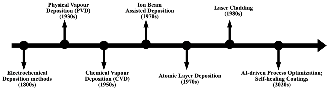
Figure 2.
Schematic of conventional PVD processes: (a) sputtering and (b) evaporating using ionized Argon (Ar+) gas. Reprinted with permission from ref. [4].
Figure 2.
Schematic of conventional PVD processes: (a) sputtering and (b) evaporating using ionized Argon (Ar+) gas. Reprinted with permission from ref. [4].
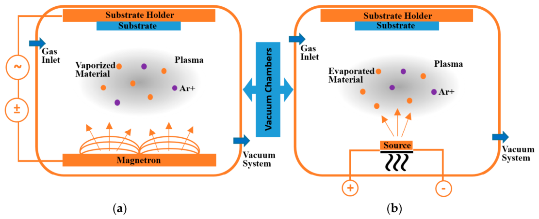
Figure 3.
Fracture cross-sectional SEM images (a–c), FIB secondary electron images of cross-sections (d–f), and FIB secondary electron top view images (g–i) of TiN coatings deposited by low-voltage electron beam evaporation (BAI), magnetron sputtering (CC7) and cathodic arc deposition techniques (AIP). Reprinted with permission from ref. [22]. Copyright 2020 AIP Publishing.
Figure 3.
Fracture cross-sectional SEM images (a–c), FIB secondary electron images of cross-sections (d–f), and FIB secondary electron top view images (g–i) of TiN coatings deposited by low-voltage electron beam evaporation (BAI), magnetron sputtering (CC7) and cathodic arc deposition techniques (AIP). Reprinted with permission from ref. [22]. Copyright 2020 AIP Publishing.
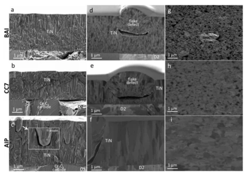
Figure 4.
Wear rates of BAI, CC7 and AIP coatings as a function of surface roughness Sa. The wear tests were performed in (a) nitrogen (b) ambient air and (c) oxygen atmospheres. Reprinted with permission from ref. [22].
Figure 4.
Wear rates of BAI, CC7 and AIP coatings as a function of surface roughness Sa. The wear tests were performed in (a) nitrogen (b) ambient air and (c) oxygen atmospheres. Reprinted with permission from ref. [22].
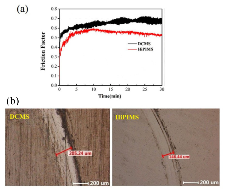
Figure 5.
(a) The friction coefficient and (b) wear groove width obtained from the friction and wear tests on CrN coatings prepared via HiPIMS and DCMS. Reprinted with permission from ref. [25].
Figure 5.
(a) The friction coefficient and (b) wear groove width obtained from the friction and wear tests on CrN coatings prepared via HiPIMS and DCMS. Reprinted with permission from ref. [25].
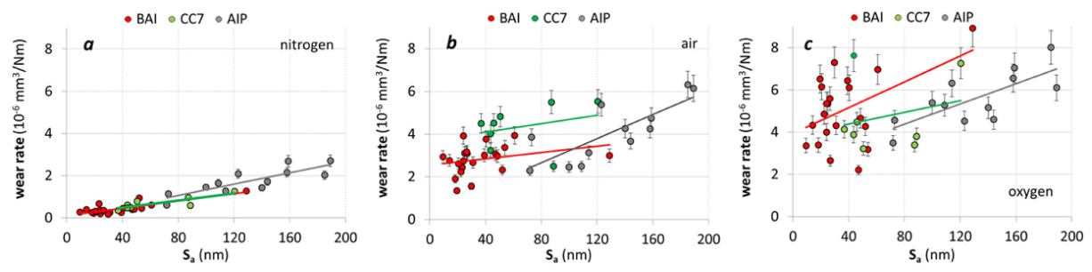
Figure 6.
Laser cladding using powdered feedstock. Adapted from webpage: https://www.laserline.com/en-int/laser-cladding/.
Figure 6.
Laser cladding using powdered feedstock. Adapted from webpage: https://www.laserline.com/en-int/laser-cladding/.
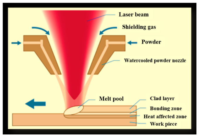
Figure 7.
Schematic of the main steps of the CVD process. Reprinted with permission from ref. [115].
Figure 7.
Schematic of the main steps of the CVD process. Reprinted with permission from ref. [115].
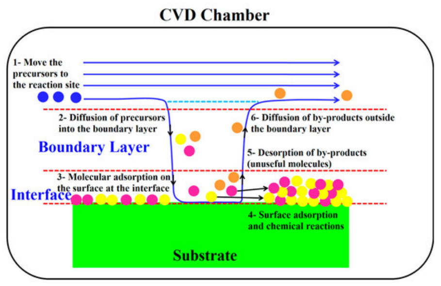
Figure 8.
Electron micrographs of conformal coverage of iCVD polymers over complex geometries. SEM images of TiO2 nanopillars (a) before and (b) after CSE95 deposition, TiO2 nanopores (c) before and (d) after CSE10 deposition, and CSE10 coated. Reprinted with permission from ref. [124]. Copyright 2019 American Chemical Society.
Figure 8.
Electron micrographs of conformal coverage of iCVD polymers over complex geometries. SEM images of TiO2 nanopillars (a) before and (b) after CSE95 deposition, TiO2 nanopores (c) before and (d) after CSE10 deposition, and CSE10 coated. Reprinted with permission from ref. [124]. Copyright 2019 American Chemical Society.
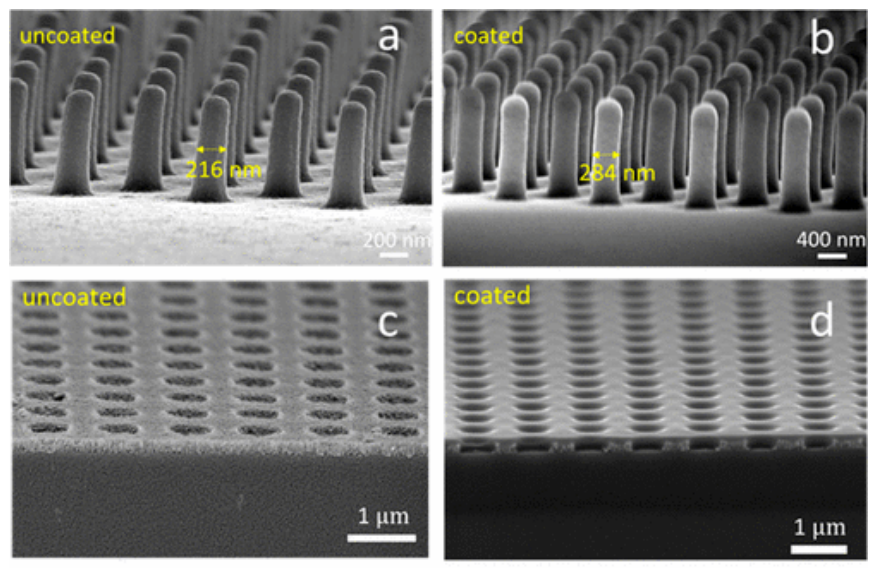
Figure 10.
Schematic of a three-staged deposition process of the layered degradable coating using iCVD. Sequentially deposited were PDE as the antibacterial layer, PMAH or its copolymer as the biodegradable layer, and another PDE antibacterial layer. Reproduced with permission from ref. [166]. Copyright 2021 American Chemical Society.
Figure 10.
Schematic of a three-staged deposition process of the layered degradable coating using iCVD. Sequentially deposited were PDE as the antibacterial layer, PMAH or its copolymer as the biodegradable layer, and another PDE antibacterial layer. Reproduced with permission from ref. [166]. Copyright 2021 American Chemical Society.
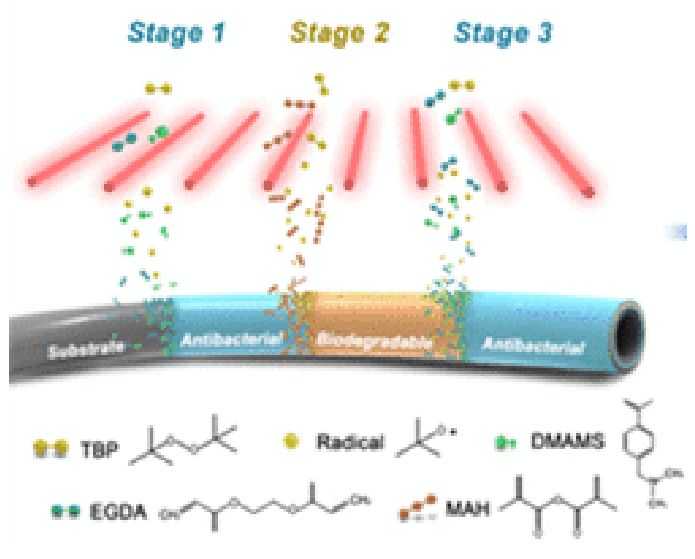
Figure 11.
Schematic illustration of a typical ALD cycle. Reprinted with permission from ref. [175]. Copyright 2026 Wiley-VCH GmbH.
Figure 11.
Schematic illustration of a typical ALD cycle. Reprinted with permission from ref. [175]. Copyright 2026 Wiley-VCH GmbH.
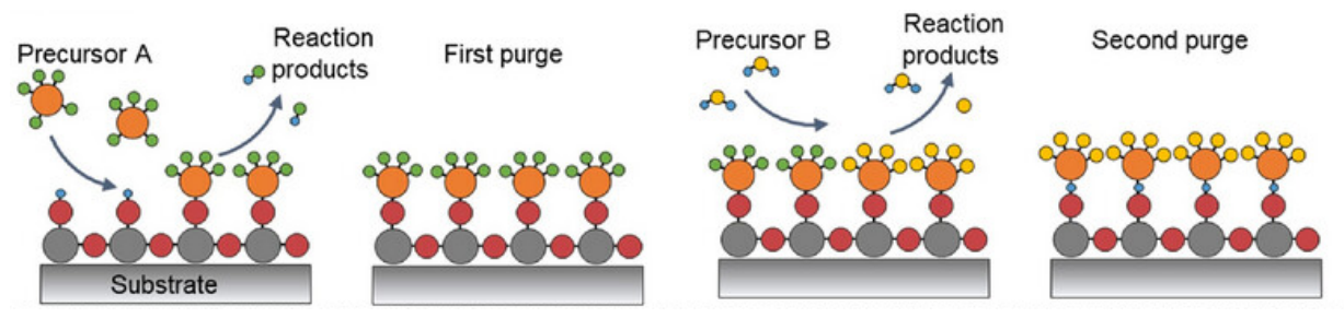
Figure 12.
Scanning electron microscopy image of an SiO2 film deposited using a bis(tert-butylamino)silane (SiH2(NHtBu)2, BTBAS) and O2 plasma ALD process at 400 °C on a nanostructure with an aspect ratio of ∼4.5. ref. [188]. Copyright 2018 Americal Chemical Society.
Figure 12.
Scanning electron microscopy image of an SiO2 film deposited using a bis(tert-butylamino)silane (SiH2(NHtBu)2, BTBAS) and O2 plasma ALD process at 400 °C on a nanostructure with an aspect ratio of ∼4.5. ref. [188]. Copyright 2018 Americal Chemical Society.
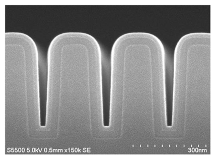
Figure 13.
(a) Low-temperature ALD-grown 10 cm × 10 cm sample with 2 cm × 2 cm reticles and (b) ZnO TFT array. ref. [189]. Copyright 2025 Americal Chemical Society.
Figure 13.
(a) Low-temperature ALD-grown 10 cm × 10 cm sample with 2 cm × 2 cm reticles and (b) ZnO TFT array. ref. [189]. Copyright 2025 Americal Chemical Society.
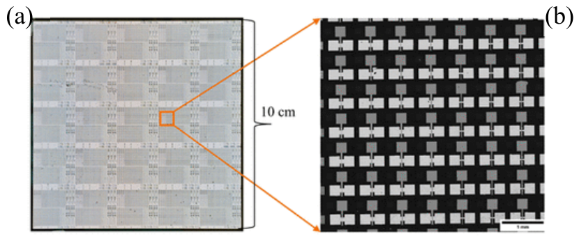
Figure 14.
Load vs displacement curves for (a) Cu (40 nm)/NbCx (2.6 nm)/SiO2 (100 nm) and (b) Ru (40 nm)/NbCx (2.6 nm)/SiO2 (100 nm) structures. (c) TEM image of the 3D trench substrate (depth: 400 nm; bottom width: ∼275 nm) coated by the PEALD-grown NbC layer. Reprinted with permission from ref. [190]. Copyright 2025 Americal Chemical Society.
Figure 14.
Load vs displacement curves for (a) Cu (40 nm)/NbCx (2.6 nm)/SiO2 (100 nm) and (b) Ru (40 nm)/NbCx (2.6 nm)/SiO2 (100 nm) structures. (c) TEM image of the 3D trench substrate (depth: 400 nm; bottom width: ∼275 nm) coated by the PEALD-grown NbC layer. Reprinted with permission from ref. [190]. Copyright 2025 Americal Chemical Society.
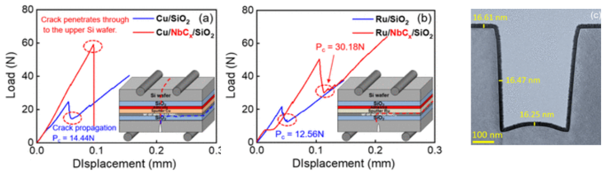
Figure 15.
a) Photograph of the highly transparent and flexible device in a bent state. (b) Schematic of the flexible ITO FeFET memory devices. (c) The key experimental method flow of HZO-based FeFET fabrication process. (d) HRTEM image of the Ni/ITO/HZO/W/Ti/Al2O3 gate stack. HRTEM shows clear crystallization of the HZO material and an ultra-thin 3.4 nm ITO channel. Reprinted with permission from ref. [191].
Figure 15.
a) Photograph of the highly transparent and flexible device in a bent state. (b) Schematic of the flexible ITO FeFET memory devices. (c) The key experimental method flow of HZO-based FeFET fabrication process. (d) HRTEM image of the Ni/ITO/HZO/W/Ti/Al2O3 gate stack. HRTEM shows clear crystallization of the HZO material and an ultra-thin 3.4 nm ITO channel. Reprinted with permission from ref. [191].
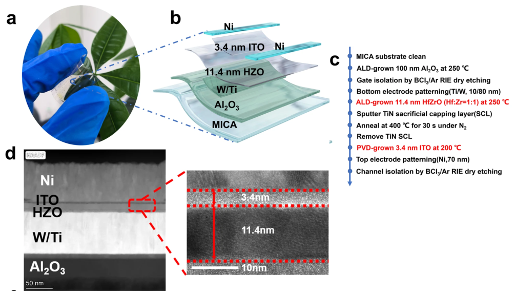
Figure 16.
XRF thickness maps of the Sn-Ru deposit. (a) direct current sample 1 A/dm2, (b) pulsed current 2 ms, (c) pulsed current 5 ms, (d) pulsed current 10 ms, (e) pulsed reverse current 2 ms, (f) pulsed reverse current 5 ms, (g) pulsed reverse current 10 ms. Reprinted with permission from ref. [269].
Figure 16.
XRF thickness maps of the Sn-Ru deposit. (a) direct current sample 1 A/dm2, (b) pulsed current 2 ms, (c) pulsed current 5 ms, (d) pulsed current 10 ms, (e) pulsed reverse current 2 ms, (f) pulsed reverse current 5 ms, (g) pulsed reverse current 10 ms. Reprinted with permission from ref. [269].
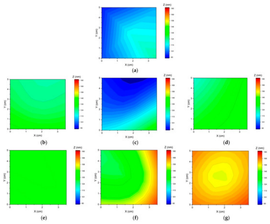
Disclaimer/Publisher’s Note: The statements, opinions and data contained in all publications are solely those of the individual author(s) and contributor(s) and not of MDPI and/or the editor(s). MDPI and/or the editor(s) disclaim responsibility for any injury to people or property resulting from any ideas, methods, instructions or products referred to in the content. |
© 2026 by the authors. Licensee MDPI, Basel, Switzerland. This article is an open access article distributed under the terms and conditions of the Creative Commons Attribution (CC BY) license (http://creativecommons.org/licenses/by/4.0/).
Copyright: This open access article is published under a Creative Commons CC BY 4.0 license, which permit the free download, distribution, and reuse, provided that the author and preprint are cited in any reuse.


