
Submitted:
07 July 2026
Posted:
08 July 2026
You are already at the latest version
Abstract
In this work, we present a methodology for determining the interface-state density distribution in metal-insulator-semiconductor (MIS) AlGaN/GaN heterostructures using sub-bandgap illumination. First, we discuss the electronic transitions that occur during sub-bandgap illumination of MIS AlGaN/GaN heterostructures. In particular, we show how these transitions can induce a threshold-voltage shift in MIS AlGaN/GaN HEMT structures and, consequently, lead to a completely erroneous interpretation of the results. In this context, we experimentally demonstrate that the interface-state density distribution can be significantly overestimated due to, for example, free-hole generation resulting from electronic transitions via interface states at the AlGaN/insulator interface and/or deep levels in the GaN buffer layer. Finally, we provide guidelines for the accurate determination of the interface-state density in MIS AlGaN/GaN heterostructures using sub-bandgap illumination, including detailed measurement and analysis procedures.
Keywords:
GaN
; Interface states
1. Introduction
The interface states at insulator/AlxGa1−xN interfaces have a significant impact on the operation of AlGaN/GaN high electron mobility transistors (HEMTs)[1,2,3] as well as on the GaN MOSFETs[4,5]. In particular, high interface state density may cause a strong "current collapse" effect, threshold voltage instability, and high leakage current[6,7,8,9,10,11,12,13,14,15,16] Therefore, to improve the performance of AlGaN/GaN HEMTs, it is important to control the interface traps at insulator/AlGaN interfaces. In this context, the quantitative characterization of their electronic properties is one of the main goals of research. However, in the case of wide bandgap semiconductors like AlGaN, standard electric methods like the Terman method fail because of an extremely long electron emission time () to the conduction ban (CB) at room temperature. For example, for a trap located at 1 eV, can be estimated as 28 h[17].
To address this issue, several groups proposed non-standard photoelectric methods based on above or/and sub-band gap illumination of AlGaN/GaN metal-insulator-semiconductor (MIS) structures[18,19,20,21,22,23,24,25,26]. Although these methods can provide information on the interface states located at midgap, their require specific experimental conditions and their accuracy (in most cases) were not verified yet. In this work, we present a unified methodology for characterizing interface states in these heterostructures using sub-band gap light. Specifically, we describe measurement and analysis procedures for determining the interface state density and demonstrate how to avoid common errors in the interpretation of photo-assisted capacitance-voltage (C-V) curves for MIS AlGaN/GaN heterostructures.
The paper is organized as follows. In Sec. 2, we briefly describe the fabrication process of the MIS AlGaN/GaN heterostructures used in this study and the experimental details of the photo-assisted capacitance-voltage (C-V) measurements. In Sec. 3, we discuss sub-band gap electronic transitions and their role in the threshold voltage shift. In Sec. 4, we present our methodology for determining the interface state density using sub-band gap illumination. Finally, in Sec. 5, we conclude with a short discussion of the main points of this paper.
2. Sample Structure and Sub-Band Gap Illumination Experimental Details
For the purpose of this paper, we used the MIS and Schottky AlGaN/GaN HEMT structures, which are shown schematically in Figure 1. The epitaxial AlGaN/GaN heterostructure was grown on a 3-in. semi-insulating SiC substrate using a horizontal flow metalorganic vapor phase epitaxy (MOVPE) reactor. In detail, the epi-structure contains a 5 nm GaN cap layer, a 14-nm Al0.22Ga0.78N barrier, a 1000-nm GaN channel, and a 300 nm Fe-doped GaN buffer. For passivation, we used the following dielectric stack: SiN: (50 nm) + SiON: (20 nm) grown by plasma-enhancement chemical vapor deposition. The deposition temperature for SiN was 250 oC. The SiON layer was formed from SiO2 by adding NH3 during growth of SiO2. Regarding the experiment, photo-assisted C–V curves were obtained at 1 MHz using an impedance analyzer at room temperature. A 150 W halogen lamp with bandpass filters was applied as a light source[17].
3. Sub-Band Gap Electronic Transitions and Threshold Voltage of MIS AlGaN/GaN HEMTs
This section includes a description of the sub-band gap electronic transitions in AlGaN/GaN heterostructures and their impact on the threshold voltage of MIS AlGaN/GaN HEMTs.
3.1. Absorption of Sub-Band Gap Light at Interface States
Before discussing sub-bandgap electronic transitions, we need to address a challenge that is typically overlooked in most approaches to characterizing interface states in MIS AlGaN/GaN heterostructures. Most methods assume that sub-band gap light is mainly absorbed at the insulator/AlGaN interface. In other words, sub-band gap illumination of a MIS AlGaN/GaN structure is thought to lead to the excitation of electrons primary from interface states, while the excitation of electrons from GaN buffer layer is largely ignored. However, there are no reports on the optical cross section of interface states at the insulator/AlGaN interface. Furthermore, surface photovoltage studies from non-passivated GaN surface show that the optical cross-sections of surface states are very low[27]– on the order of 10−18cm−2 (for a light energy of 2.3 eV)– which is several orders of magnitude lower than for bulk states[28]. This suggests that the surface states are practically optically inactive compared to deep-level states in the GaN. Therefore, to avoid the issue of sub-bandgap light absorption at deep levels, any proposed photoelectric method must clearly distinguish between the contributions from deep levels in the GaN buffer layer and those from interface states at the insulator/AlGaN interface.
3.2. Electronic Transitions Leading to the Generation of Free Holes in AlGaN/GaN Heterostructures
The first kind of sub-bandgap electronic transitions- and perhaps the most important- are those that generate free holes in MIS AlGaN/GaN HEMT structures. As shown below, these transitions can lead to a completely erroneous interpretation of the threshold voltage shift in these devices under sub-bandgap illumination.
Figure 2(a) shows the band diagram of an MIS AlGaN/GaN heterostructure biased at (below the threshold voltage (Vth) and illuminated with sub-bandgap light. Such experimental conditions, i.e. illumination of an MIS AlGaN/GaN heterostructure polarized below the threshold, are typically applied in various photoelectric methods[19,29]. In the conventional model (optimistic scenario), the sub-bandgap light is absorbed at interface states, leading to the excitation of an electron to CB (process 1). Due to this process, the occupation of interface states is changed, and a threshold voltage shift (Vth) is induced during a C-V sweep from reverse to forward bias, as shown in the inset of Figure 2(a). However, the same light can also lead to the excitation of electrons from the valence band (VB) to empty interface state (process 2, Figure 2(b)) and the generation of free holes in the valance band. Subsequently, the electrons excited to the empty interface states can be thermally excited to CB (process 3, Figure 1(b)). Consequently, the interface states due to process 2 and 3 do not change their occupation, but remaining holes in VB cause a similar Vth as that in process 1 (inset of Figure 2(a)).
In the next scenario, light can induce an internal transition between the interface states (Figure 2(c). This process can be particularly important when interface states are continuously distributed within the band gap. In particular, sub-bandgap light can induce a transition of an electron from a donor-like state to an acceptor-like sate (process 4, Figure 2(c)). Subsequently, the electron from the acceptor-like state can be thermally excited to CB (process 5, Figure 2(c)), while the empty donor-like state can be reoccupied by an electron from VB (process 6, Figure 2(c)). Because of these processes, as previously described, a free hole remains in VB leading to a similar Vth as in process 1 (inset of Figure 2(a)).
The processes described in Figure 2(a)-(c) demonstrate that it is challenging to identify which interface state is responsible for Vth after illumination. Therefore, linking Vth obtained under illumination of an MIS AlGaN/GaN heterostructure biased below the threshold voltage to a specific interface state energy distribution () can be questionable. In particular, the following equation, often applied for determining , may not be appropriate[19]:
where is difference between two C–V curves with two photon energies hv1 and hv2, is the series capacitance of insulator and AlGaN, hv is the energy difference between hv1 and hv2 and is the average interface energy.
In addition to the free holes generated via interface states, transition through deep levels in GaN can also induce the free holes and cause the Vth in C-V curves. As shown in Figure 3, sub-bandgap light excites electrons from deep acceptors located in the GaN buffer layer (process 7). This excitation empties the acceptor states, allowing electrons from VB to occupy them (process 8), which leaves holes in VB. Consequently, these free holes are attracted to the AlGaN/GaN interface (process 9, Figure 3) or/and to the insulator/AlGaN interface (process 10) where they accumulate if is sufficiently negative. The additional positive charge at the AlGaN/GaN and insulator/AlGaN interface resulting from the accumulation of free holes, can lead to the Vth shift in C-V curves, as shown in the inset of Figure 3. This shift may occur in the same direction as that arising from process 1 (inset of Figure 1(a)) assuming that acceptor-like states are depopulated during process 1. Consequently, processes 7, 8, 9, and 10 can lead not only to an overestimation of the interface state density calculated from Eq. 1 but also to a completely incorrect interpretation of the Vth shift in C-V curves.
To illustrate the effect of free-hole generation on the threshold voltage of the AlGaN/GaN MIS structure and the determination of from Eq. 1, we performed the following experiment. The AlGaN/GaN MIS structure was illuminated for 60 s at gate bias, VGL, (below the threshold voltage of the AlGaN/GaN MIS structure) with light at an energy of 2.2 eV. After switching off the light, the gate bias was swept toward +2 V under dark conditions and Vth (i.e., the difference of threshold voltage between the post-illumination C-V curve and the dark one) was obtained (Figure 4(a)). This process was repeated for different VGL values, and the results are summarized in Figure 4(b). As can be seen from this figure, when VGL becomes more negative, Vth increases. It should be noted that this effect is not related to the shift of C-V curves due to the bias stress at VGL, since the dark C-V curves do not change their position after holding the bias at VGL for 60 s (see Figure 4(a) and curve A after the bias stress at VGL = -20 V under dark conditions). The only explanation for this effect is that when VGL becomes more negative, more free holes (generated due to electronic transitions via deep levels in the GaN buffer layer; see Figure 3) are attracted toward the AlGaN/GaN and insulator/AlGaN interfaces (see Figure 3), thereby increasing the positive charge at these interfaces and, consequently, Vth. In this context, it is interesting to note that the observed behavior of Vth vs. VGL for the AlGaN/GaN MIS structure is quite different from that of the AlGaN/GaN Schottky barrier diode (SBD). In the case of AlGaN/GaN SBD structure, we observed a decrease in Vth when VGL become more negative. This is consistent with the free-hole explanation, since for AlGaN/GaN SBD structure, free holes generated due to electronic transitions via deep levels in the GaN buffer layer flow directly to the gate metal if VGL is negative enough and no additional positive charge remains in the structure.
Next, we performed the same experiment but with a light energy of 2.4 eV. The results of this experiment were summarized in Figure 4(b). Similar to the previous case, the Vth increases as VGL becomes more negative. However, in this case, the dependence of Vth vs. VGL is different - significantly stronger (likely due to the generation of more free holes at 2.4 eV). Consequently, when we applied Eq. 1 (with the determined Vth for 2.2 eV and 2.4 eV and =110 nF/cm2), we obtain different values of vs. VGL, as shown in Figure 4(c). It should be noted that these determined values vary by an order of magnitude, from 1012 to 1013cm−2eV−1, depending on VGL. This experiment clearly shows that it is difficult to accurately determine the interface state density at the insulator/AlGaN interface when the AlGaN/GaN MIS structure is illuminated at a gate bias below the threshold voltage.
3.3. Electronic Transitions Witch Does Not Change the Interface-State Charge
In some cases, Vth cannot be observed under illumination at a certain energy. This effect is commonly attributed to a low interface state density or a discrete distribution of interface states. However, as we show below, this effect can be related to internal transitions between the interface states. Similarly to Figure 1(c), the sub-bandgap light causes an electron transition from donor-like state to acceptor-like state (see process 11, Figure 5(a)). However, in this scenario the transition occurs between the states around the mid-gap. For such states, the thermal energy is insufficient to excite an electron from VB to empty donor-like state, or from an acceptor-like state to CB, as in Figure 1(c). As a consequence, the total charge of the interface states does not change, since the donor-like states become positive and the acceptor-like states become negative due to the electron transition. Consequently, Vth may not be observed, as shown in the inset of Figure 5(a).
3.4. Transitions from Deep Levels in the AlGaN Barrier to Interface States
Another type of transition that can also lead to Vth and is not related to the depopulation of interface states is the electronic transition of electron from deep levels in the AlGaN barrier to empty interface states. In this case, electrons from defect states in the AlGaN barrier are excited to higher energies within CB due to sub-bandgap illumination (process 12, Figure 5(b)). Due to process 12, the electrons can overcome the surface potential barrier and be trapped in the empty interface states (process 13, Figure 5(b)), leading to an increase in the negative interface state charge and Vth. However, in this scenario, Vth will be in opposite direction to that shown in the inset of Figure 1(a). This kind of transition is commonly observed in surface photovoltage measurements and should be significant in the case of long-wavelength illumination.
4. Guidelines for Determination of Interface State Density in MIS AlGaN/GaN Structures
We now provide our methodology for the determination of interface state density in AlGaN/GaN MIS structures. The proposed methodology allows us to avoid the problems described in Sec. III. In particular, by using this technique, we can obtain a direct photo-response from the interface states at the insulator/AlGaN interface, while ignoring effects from deep levels in the GaN buffer layer.
Contrary to the experimental conditions commonly applied in photo-assisted C-V experiments, in our methodology, the AlGaN/GaN MIS structure is illuminated at a gate bias (VG1) at which a two-dimensional (2D) electron gas is present at the AlGaN/GaN interface[24,30]. As we show below, only under such experimental conditions, we obtain Vth related to the interface states at the insulator/AlGaN interface. Figure 6(a) shows the band diagram of the AlGaN/GaN MIS heterostructure polarized at VG1 and illuminated with sub-bandgap light. We assumed that sub-bandgap light leads to the excitation of electrons from interface states at the insulator/AlGaN interface, as well as to the generation of free holes from bulk deep levels in the GaN buffer layer via electronic transitions described in Sec. III (see Figure 3). However, in this case, instead of being attracted toward the insulator/AlGaN interface, like in Figure 3, the free holes are repelled into the bulk (process 14, Figure 6(a)), since the structure is polarized at VG1 where accumulation in GaN is present. Consequently, the generated free holes from the deep levels do not participate in Vth. Therefore, we can obtain Vth related mainly to the depopulation of the interface states at the insulator/AlGaN interface.
The detailed experimental procedure is the following. Before illumination, we swept the gate voltage from negative to positive bias to fill the interface states with electrons (step 1 in Figure 6(b)). Next, the gate bias was swept from accumulation to (step 2 in Figure 6(b)) (for which a 2D electron gas is present at the AlGaN/GaN interface). Keeping the bias , the AlGaN/GaN MIS heterostructure was illuminated by the sub-bandgap light (in this case 2.2 eV) for approximately 10 min (previous experiments show that such time is suitable for saturation of ). After turning off the light, the gate bias was swept from to depletion (step 3, Figure 6(b)) and Vth was obtained. We then repeated all the above steps for different VG1 (between 0 to threshold voltage), and the results, i.e., dependencies of Vth vs. VG1, were summarized in Figure 7(a) and (b). Compared to the previous case (see Figure 4(b)), here Vth practically does not depend on VG1 (see Figure 7(a)). Similar results were obtained for light with an energy of 2.4 eV (Figure 7(b)), i.e., independent Vth on the bias at which illumination occurs. This indicates that free holes generated in the GaN buffer do not participate as previously in Vth. Now, if we use Eq. 1 with determined Vth for 2.2 eV and 2.4 eV (Figure 7(b)), we get a very reasonable value of = 8×1011cm−2eV−1(Figure 7(c)), independent on the gate bias at which illumination occurs.
Finally, it remains only to verify whether the obtained Vth does not originate from holes generated by electronic transitions via interface states at the AlGaN/insulator (see Figure 1(b)). The minimal criterion to exclude this possibility is to check the position of the threshold voltage after illumination. If, after illumination, the threshold voltage returns to its initial position, we can conclude that free holes were likely not generated at the AlGaN/insulator interface. In the opposite case- i.e., when the threshold voltage does not return to its original value- it is likely that free holes were formed at the AlGaN/insulator interface. From a physical point of view, free holes accumulated at the AlGaN/insulator interface can tunnel into the insulator, especially at large negative biases (after illumination, the gate bias is swept toward negative values below the threshold voltage, see Figure 6(b)). As a result, they may remain in the insulator, and the threshold voltage might not return to the original position even after many restarts. In our case, the threshold voltage always returns to its original position prior to illumination, as shown in Figure 7(b). Therefore, we can conclude that the obtained Vth mainly originates from the excitation of electrons from interface states to CB due to process 1 (see Figure 1(a)).
All the above procedures are summarized in the flowchart shown in Figure 8. First, we select a gate bias, (from the range between 0 V and the threshold voltage) at which sub-bandgap illumination is applied. Subsequently, we perform photo-assisted C–V measurements using light with photon energy (as shown in Figure 6(b)) to determine . We then repeat the above steps for different values of (but at the same photon energy, ) to obtain the dependence of on . If this dependence is constant, i.e., if does not depend on , free holes most likely do not contribute to . Conversely, if (i) increases with , free holes affect , or (ii) decreases with , electron emission from interface states in the dark state occurs during variations of . Regardless of which scenario [(i) or (ii)] is observed, all measurements should be repeated using a different incident photon energy.
After verifying that the dependence of Vth vs. VG1 is constant, we check whether the threshold voltage returns to its original position prior to illumination (like in Figure 7(b)). If so, we can conclude that the obtained Vth originates from the excitation of electrons from the interface state to CB due to process 1 (see Figure 1(a)), and we can use this value to determine from Eq. 1. If not, the situation is unclear, and obtained Vth cannot be used to determine .
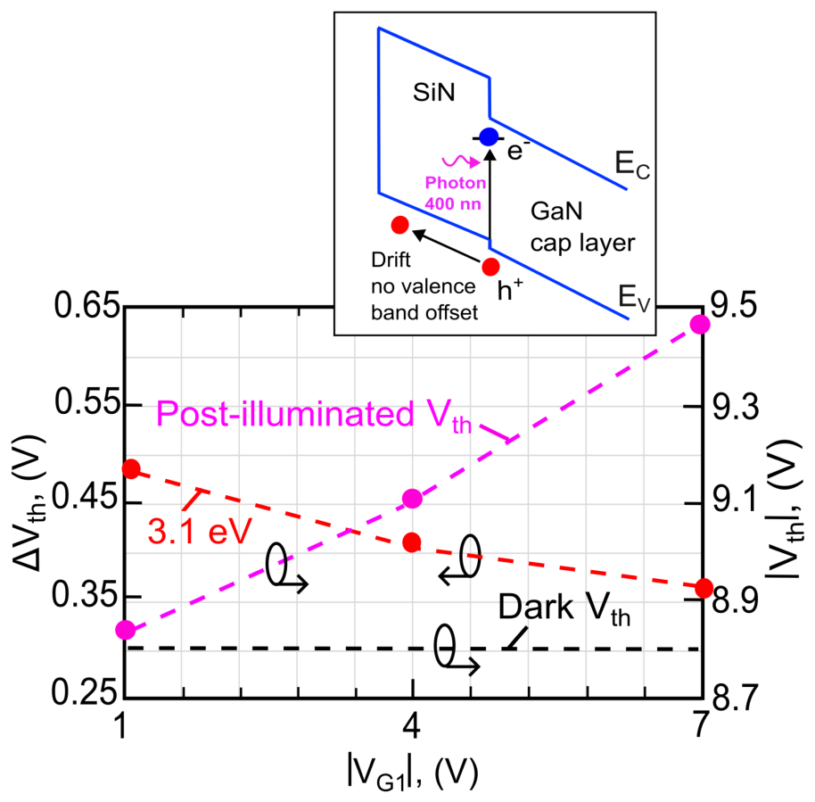
It is also interesting to verify what happens when shorter wavelengths, i.e., wavelengths closer to the GaN band edge, are applied while the AlGaN/GaN heterostructure is illuminated at a gate bias , at which a two-dimensional electron gas (2DEG) is formed at the AlGaN/GaN interface. Figure 9 shows the dependence of on for a photon energy of 3.1 eV (400 nm). In this case, decreases with increasing , and the threshold voltage does not return to its initial value after illumination, as shown in Figure 9. These results can be understood as follows. Under sub-bandgap illumination with a wavelength close to the GaN band edge, free holes are generated at the SiN/GaN interface, in a manner similar to that illustrated in Figure 2(b) and 2(c). Subsequently, these holes are attracted toward the gate metal (as schematically shown in the inset of Figure 9) because the valence-band offset between SiN and GaN is zero or negative [32]. Therefore, according to the proposed methodology (Figure 8), illumination at 400 nm fails the verification steps. Consequently, the algorithm would conclude that the obtained data, i.e., under 400 nm illumination cannot be used to determine the interface-state density, , from Eq. (1).
4.1. Discussion and Conclusions
Most of the problems related to free-hole generation can be addressed using the methodology described in Sec. IV. In particular, by applying this approach, it is not necessary to consider the issue of optical absorption (see Sec. IIIA), since the contribution of deep levels in the GaN buffer layer can be clearly distinguished from that of interface states at the insulator/AlGaN interface. However, the proposed methodology cannot exclude transitions from deep levels to interface states [Figure 5(b)]. Nevertheless, we believe that such transitions should induce a shift in the opposite direction to that shown in Figure 1(a).
In this paper, we also neglect other effects that may contribute to under sub-bandgap illumination. For example, long-wavelength light may excite hot electrons from the 2DEG at the AlGaN/GaN interface, leading to a threshold-voltage shift through self-heating effects [31]. In the discussion presented in Sec. III, we likewise omitted effects associated with the insulator, such as the excitation of border traps and bulk traps by sub-bandgap illumination. These processes can clearly contribute to . However, the influence of bulk insulator traps can be excluded by measuring the product [24] for different insulator thicknesses (d). If bulk insulator traps are excited by sub-bandgap illumination, the product should exhibit a strong dependence on d. Conversely, if is nearly independent of d, the contribution of bulk insulator traps to can be considered negligible. In conclusion, the main findings of this work are summarized as follows:
I. Sub-bandgap illumination of an AlGaN/GaN MIS heterostructure biased below the threshold voltage (see Figure 1) does not provide information about the interface states at the insulator/AlGaN interface; rather, it reflects the concentration of free holes generated in the GaN buffer layer through electronic transitions via deep levels (see Figure 3 and Figure 4). This effect becomes particularly significant when the photon energy exceeds one-half of the GaN bandgap energy.
II. For an accurate estimation of the interface-state density at the insulator/AlGaN interface, the AlGaN/GaN MIS heterostructure should be illuminated at gate biases for which a 2DEG is present at the AlGaN/GaN interface (see Figure 6(a)). Only under these conditions can the contribution of free holes generated in the GaN buffer layer to the threshold-voltage shift, , be eliminated.
III. By applying the developed methodology (Sec. IV and Figure 8), most errors associated with the interpretation of sub-bandgap-light-induced threshold-voltage shifts in AlGaN/GaN MIS-HEMTs can be avoided, enabling the accurate determination of at the insulator/AlGaN interface.
Data Availability Statement
The data that support the findings of this study are available from the corresponding author upon reasonable request.
Acknowledgments
The authors expresses gratitude to Norikazu Nakamura for his kind support and discussions. This work is part of the patent application number:
References
- T. Hashizume, K. Nishiguchi, S. Kaneki, J. Kuzmik, and Z. Yatabe, Mater. Sci. Semicond. Process. 78, 85–95 (2018). [CrossRef]
- U. K. Mishra, L. Shen, T. E. Kazior, and Y. F. Wu, Proc. IEEE 96, 287–305 (2008). [CrossRef]
- M. Meneghini, C. De Santi, I. Abid, M. Buffolo, M. Cioni, R. A. Khadar, L. Nela, N. Zagni, A. Chini, F. Medjdoub, G. Meneghesso, G. Verzellesi, E. Zanoni, and E. Matioli, J. Appl. Phys. 130, 181101 (2021). [CrossRef]
- T. Kachi, Appl. Phys. Express 19, 010103 (2026). [CrossRef]
- T. Narita et al., Jpn. J. Appl. Phys. 63, 120801 (2024). [CrossRef]
- P. Lagger, C. Ostermaier, G. Pobegen, and D. Pogany, in IEDM Technical Digest (2012), pp. 13.1.1–13.1.4. [CrossRef]
- T.-L. Wu, IEEE Trans. Electron Devices 63, 1853–1860 (2016). [CrossRef]
- M. Meneghini, IEEE Electron Device Lett. 37, 474–477 (2016). [CrossRef]
- C. Ostermaier, P. Lagger, M. Reiner, and D. Pogany, Microelectron. Reliab. 82, 62–83 (2018). [CrossRef]
- P. Lagger et al., Appl. Phys. Lett. 105, 033512 (2014). [CrossRef]
- D. Bisi, Appl. Phys. Lett. 108, 112104 (2016). [CrossRef]
- R. Vetury, N.-Q. Zhang, S. Keller, and U. K. Mishra, IEEE Trans. Electron Devices 48, 560–566 (2001). [CrossRef]
- M. Fagerlind, F. Allerstam, E. Ö. Sveinbjörnsson et al., J. Appl. Phys. 108, 014508 (2010).
- Y. Hori, Z. Yatabe, and T. Hashizume, J. Appl. Phys. 114, 244503 (2013). [CrossRef]
- D. Bisi, M. Meneghini, M. Van Hove, D. Marcon, S. Stoffels, T. Wu, S. Decoutere, G. Meneghesso, and E. Zanoni, Phys. Status Solidi A 212, 1122–1129 (2015). [CrossRef]
- M. Meneghini, C. De Santi, I. Abid, M. Buffolo, M. Cioni, R. A. Khadar, L. Nela, N. Zagni, A. Chini, F. Medjdoub, G. Meneghesso, G. Verzellesi, E. Zanoni, and E. Matioli, J. Appl. Phys. 130, 181101 (2021). [CrossRef]
- M. Matys, A. Yamada, Y. Kamada, and T. Ohki, APL Electron. Devices 1, 036111 (2025). [CrossRef]
- R. Yeluri, X. Liu, B. L. Swenson et al., J. Appl. Phys. 114, 083703 (2013).
- C. Mizue et al., Jpn. J. Appl. Phys. 50, 021001 (2011). [CrossRef]
- Y. Hori, C. Mizue, and T. Hashizume, Phys. Status Solidi C 9, 1356–1360 (2012). [CrossRef]
- C. M. Jackson, A. R. Arehart, E. Cinkilic et al., J. Appl. Phys. 113, 204505 (2013). [CrossRef]
- M. Ťapajna, M. Jurkovič, L. Válik, Š. Haščík, D. Gregušová, F. Brunner, E.-M. Cho, T. Hashizume, and J. Kuzmík, J. Appl. Phys. 116, 104501 (2014).
- M. Matys, B. Adamowicz, and T. Hashizume, Appl. Phys. Lett. 101, 231608 (2012). [CrossRef]
- M. Matys, B. Adamowicz, A. Domanowska, A. Michalewicz, R. Stoklas, M. Akazawa, Z. Yatabe, and T. Hashizume, J. Appl. Phys. 120, 225305 (2016). [CrossRef]
- Y. Irokawa, T. Nabatame, K. Yuge et al., AIP Adv. 9, 085311 (2019).
- B. Adamowicz, in 2021 IEEE International Meeting for Future Electron Devices, Kansai (IMFEDK) (IEEE, Kyoto, Japan, 2021), pp. 1–4. [CrossRef]
- M. A. Reshchikov, M. Foussekis, and A. A. Baski, J. Appl. Phys. 107, 113535 (2010). [CrossRef]
- T. Narita and Y. Tokuda, “Deep Levels in GaN,” in Characterization of Defects and Deep Levels for GaN Power Devices, edited by T. Narita and T. Kachi (AIP Publishing, Melville, NY, 2020), Chap. 3, pp. 3-1–3-36.
- B. Hou et al., IEEE Electron Device Lett. 39, 397–400 (2018). [CrossRef]
- M. Matys, R. Stoklas, J. Kuzmík, B. Adamowicz, Z. Yatabe, and T. Hashizume, J. Appl. Phys. 119, 205304 (2016). [CrossRef]
- M. Matys, A. Yamada, T. Ohki, and K. Tsunoda, Adv. Photonics Res. 6, 2500130 (2025). [CrossRef]
- M. Matys, B. Adamowicz, Z. R. Zytkiewicz, A. Taube, R. Kruszka, and A. Piotrowska, Appl. Phys. Lett. 109, 051106 (2016). [CrossRef]
Figure 1.
Schematic illustration of the epitaxial structure used in this study.
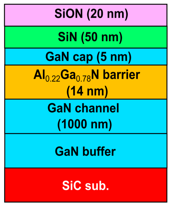
Figure 2.
Band diagrams of the MIS AlGaN/GaN structure biased under , showing various scenarios of electronic transitions via interface states at the insulator/AlGaN interface: (a) sub-bandgap illumination induces electron emission from interface states to the conduction band (CB) (process 1, conventional scenario); (b) light induces electron excitation from the valence band (VB) to an empty interface state (process 2), leaving a hole in the VB, followed by thermal excitation of the electron from the interface state to the CB (process 3); and (c) light induces an internal transition between interface states (process 4), while thermal excitation induces electron emission from an interface state to the CB (process 5) and from the VB to an empty interface state (process 6). The inset of Figure 1(a) schematically illustrates the light-induced shift in .
Figure 2.
Band diagrams of the MIS AlGaN/GaN structure biased under , showing various scenarios of electronic transitions via interface states at the insulator/AlGaN interface: (a) sub-bandgap illumination induces electron emission from interface states to the conduction band (CB) (process 1, conventional scenario); (b) light induces electron excitation from the valence band (VB) to an empty interface state (process 2), leaving a hole in the VB, followed by thermal excitation of the electron from the interface state to the CB (process 3); and (c) light induces an internal transition between interface states (process 4), while thermal excitation induces electron emission from an interface state to the CB (process 5) and from the VB to an empty interface state (process 6). The inset of Figure 1(a) schematically illustrates the light-induced shift in .
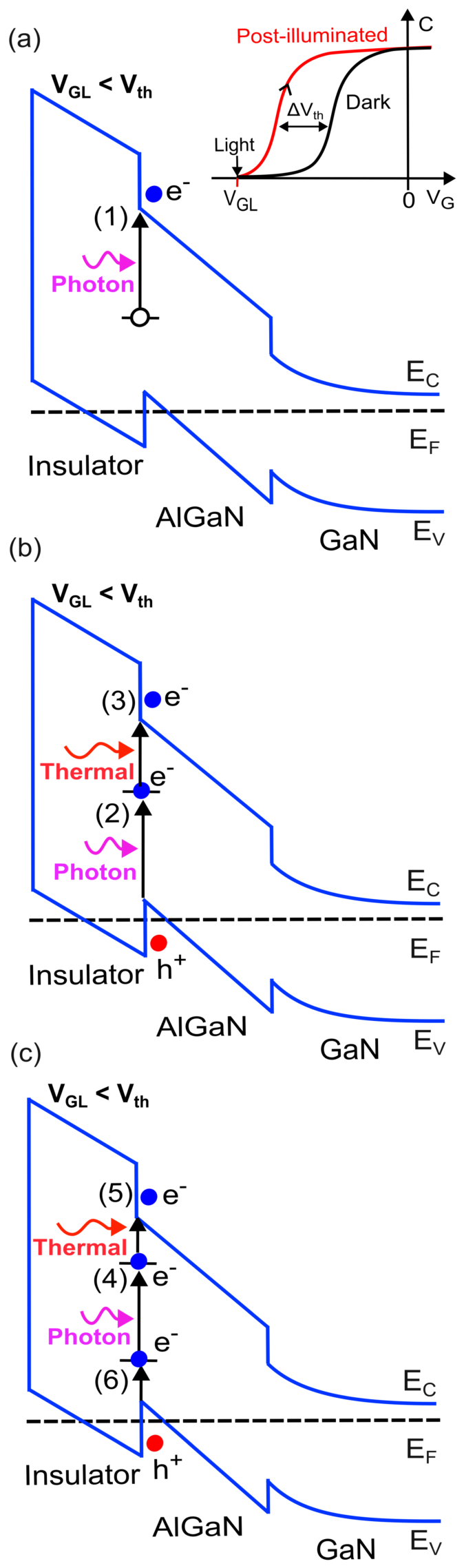
Figure 3.
Band diagram of the MIS AlGaN/GaN structure biased under , showing electronic transitions via deep levels in the GaN buffer layer. The indicated processes are as follows: process 7—light-induced excitation of an electron from an acceptor state in the GaN buffer layer to the conduction band (CB); process 8—thermal excitation of an electron from the valence band (VB) to an empty acceptor state previously depopulated by process 7; process 9—drift of free holes generated by process 8 toward the AlGaN/GaN interface; and process 10—drift of free holes toward the insulator/AlGaN interface when is sufficiently negative. The inset of Figure 2 schematically illustrates the possible shifts in the C-V curves induced by processes 9 and 10.
Figure 3.
Band diagram of the MIS AlGaN/GaN structure biased under , showing electronic transitions via deep levels in the GaN buffer layer. The indicated processes are as follows: process 7—light-induced excitation of an electron from an acceptor state in the GaN buffer layer to the conduction band (CB); process 8—thermal excitation of an electron from the valence band (VB) to an empty acceptor state previously depopulated by process 7; process 9—drift of free holes generated by process 8 toward the AlGaN/GaN interface; and process 10—drift of free holes toward the insulator/AlGaN interface when is sufficiently negative. The inset of Figure 2 schematically illustrates the possible shifts in the C-V curves induced by processes 9 and 10.
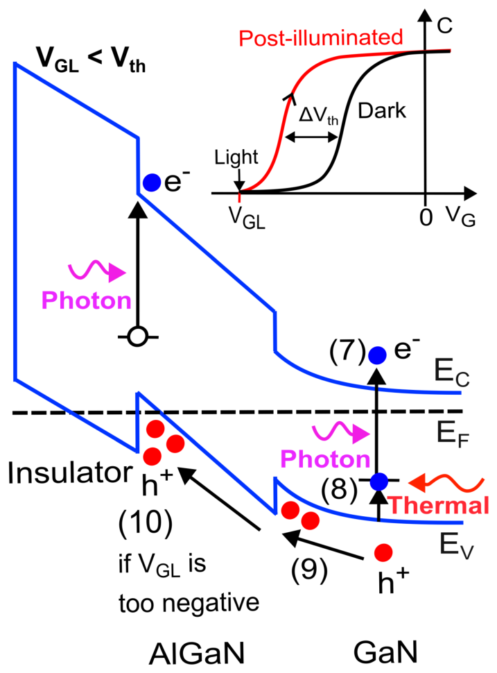
Figure 4.
(a) C-V characteristics of the investigated MIS AlGaN/GaN heterostructure measured in the dark and under illumination with light of photon energy 2.2 eV for different gate biases, V, V, and V. Curve A in Figure 3(a) shows the C–V characteristic obtained after stressing the device at V under dark conditions. (b) Dependence of on and (c) corresponding dependence of on , calculated from Figure 4(b) using Eq. (1).
Figure 4.
(a) C-V characteristics of the investigated MIS AlGaN/GaN heterostructure measured in the dark and under illumination with light of photon energy 2.2 eV for different gate biases, V, V, and V. Curve A in Figure 3(a) shows the C–V characteristic obtained after stressing the device at V under dark conditions. (b) Dependence of on and (c) corresponding dependence of on , calculated from Figure 4(b) using Eq. (1).
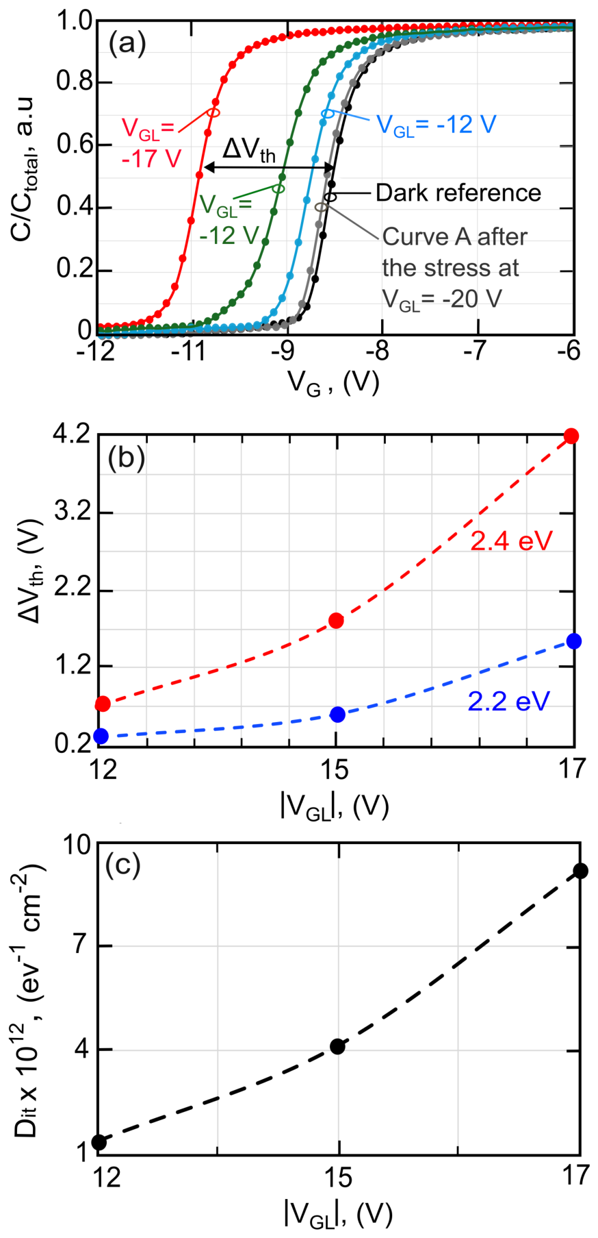
Figure 5.
Band diagrams of the MIS AlGaN/GaN structure biased under showing (a) internal electronic transitions via interface states at the insulator/AlGaN interface, which do not change the total density of interface states, and (b) electronic transitions via deep levels in the AlGaN barrier. The indicated processes are as follows: process 11—light-induced internal transition of an electron from a donor-like state to an acceptor-like state; process 12—light-induced electron transition from a deep level in the AlGaN barrier to the conduction band (CB); and process 13—trapping of the electron excited by process 12 at an interface state. The insets in Figure 5 schematically illustrate the possible shifts in the C-V curves induced by the processes described above.
Figure 5.
Band diagrams of the MIS AlGaN/GaN structure biased under showing (a) internal electronic transitions via interface states at the insulator/AlGaN interface, which do not change the total density of interface states, and (b) electronic transitions via deep levels in the AlGaN barrier. The indicated processes are as follows: process 11—light-induced internal transition of an electron from a donor-like state to an acceptor-like state; process 12—light-induced electron transition from a deep level in the AlGaN barrier to the conduction band (CB); and process 13—trapping of the electron excited by process 12 at an interface state. The insets in Figure 5 schematically illustrate the possible shifts in the C-V curves induced by the processes described above.
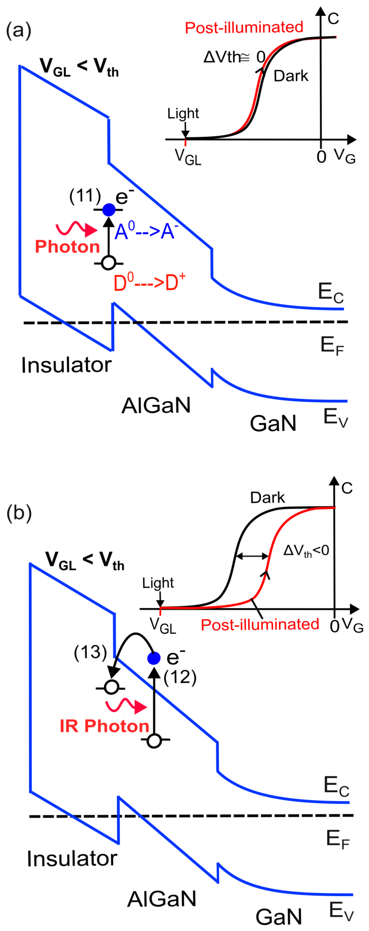
Figure 6.
(a) Band diagram of the MIS AlGaN/GaN structure biased in the range , illustrating electronic transitions via deep levels in the GaN buffer layer. Most processes are identical to those shown in Figure 3, except for process 14, which represents the drift of free holes toward the bulk GaN layer. (b) Proposed procedure for light-assisted C-V measurements.
Figure 6.
(a) Band diagram of the MIS AlGaN/GaN structure biased in the range , illustrating electronic transitions via deep levels in the GaN buffer layer. Most processes are identical to those shown in Figure 3, except for process 14, which represents the drift of free holes toward the bulk GaN layer. (b) Proposed procedure for light-assisted C-V measurements.
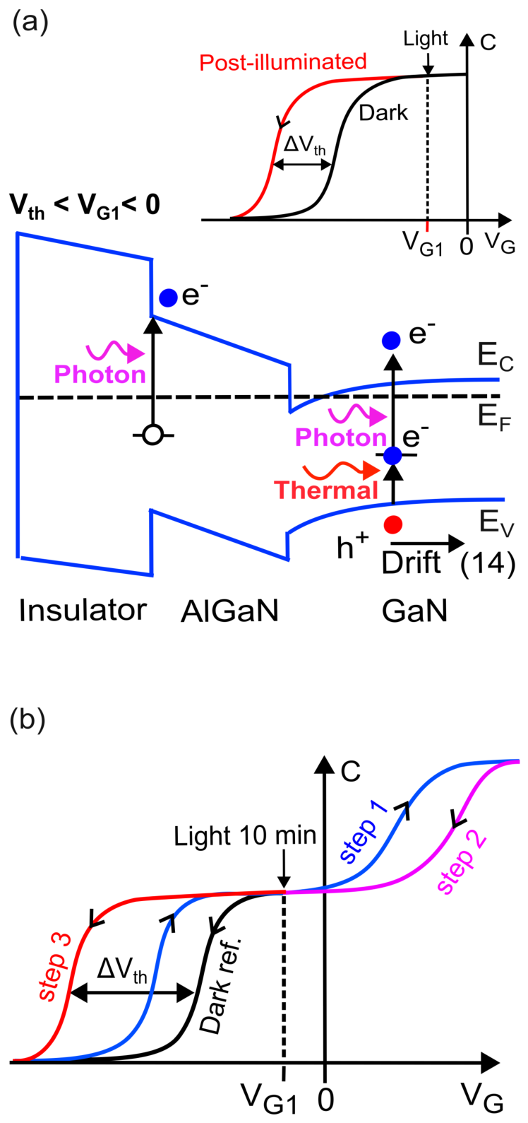
Figure 7.
(a) C-V characteristics of the investigated MIS AlGaN/GaN heterostructure measured under dark and illuminated conditions with light of photon energy 2.2 eV at different gate biases, V and V. (b) Dependence of and post-illimianted on and (c) dependence of on , calculated from Figure 7(b) using Eq. (1).
Figure 7.
(a) C-V characteristics of the investigated MIS AlGaN/GaN heterostructure measured under dark and illuminated conditions with light of photon energy 2.2 eV at different gate biases, V and V. (b) Dependence of and post-illimianted on and (c) dependence of on , calculated from Figure 7(b) using Eq. (1).
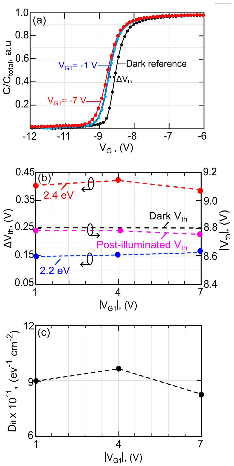
Figure 8.
Flowchart of the proposed procedure for estimation of at the insualtor/AlGaN interface.
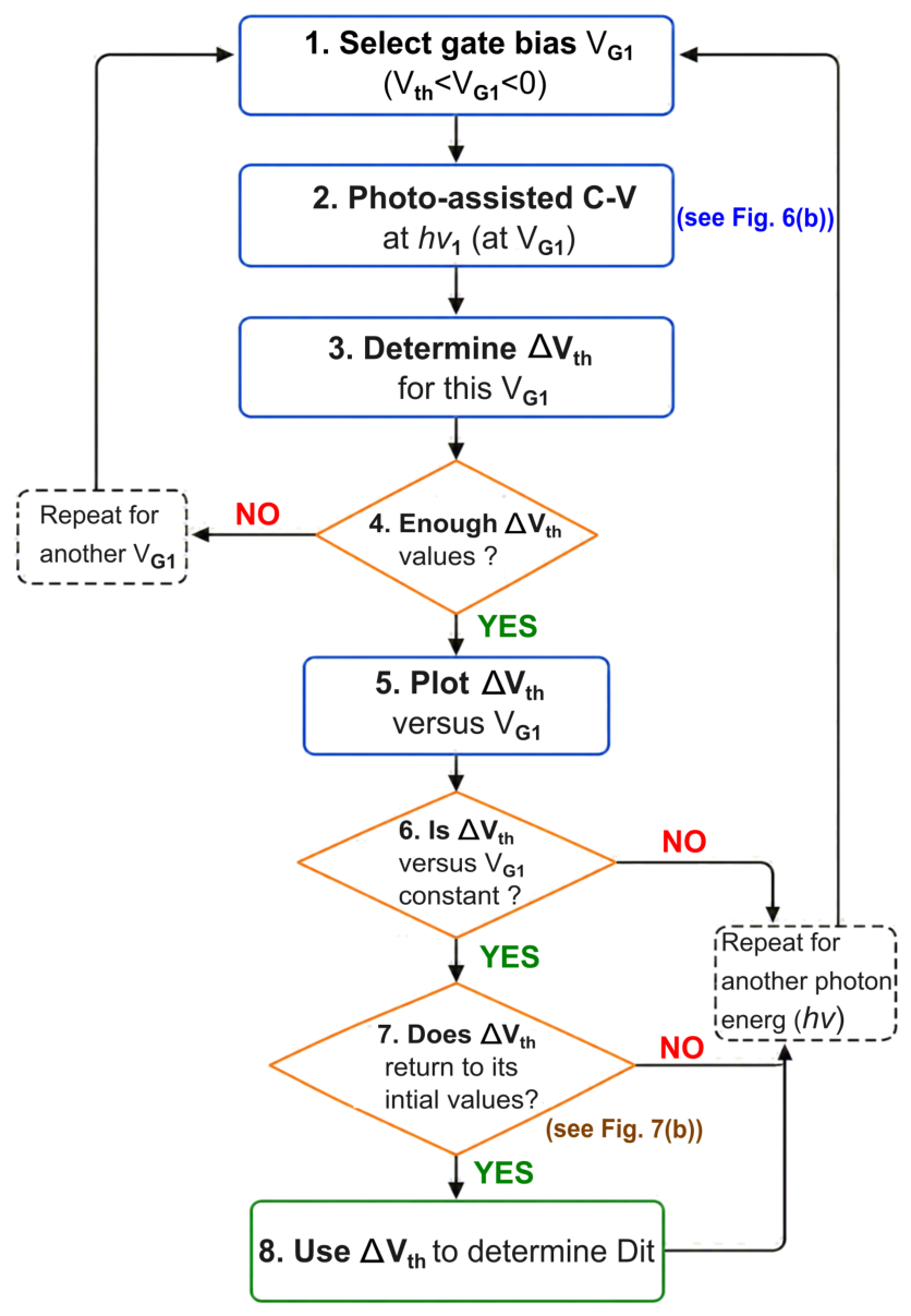
Figure 9.
Dependence of and the post-illuminated on for a photon energy of 3.1 eV. The inset schematically shows the flow of free holes from GaN into the SiN insulator.
Figure 9.
Dependence of and the post-illuminated on for a photon energy of 3.1 eV. The inset schematically shows the flow of free holes from GaN into the SiN insulator.
Disclaimer/Publisher’s Note: The statements, opinions and data contained in all publications are solely those of the individual author(s) and contributor(s) and not of MDPI and/or the editor(s). MDPI and/or the editor(s) disclaim responsibility for any injury to people or property resulting from any ideas, methods, instructions or products referred to in the content. |
© 2026 by the authors. Licensee MDPI, Basel, Switzerland. This article is an open access article distributed under the terms and conditions of the Creative Commons Attribution (CC BY) license (http://creativecommons.org/licenses/by/4.0/).
Copyright: This open access article is published under a Creative Commons CC BY 4.0 license, which permit the free download, distribution, and reuse, provided that the author and preprint are cited in any reuse.


