

Submitted:
24 June 2026
Posted:
25 June 2026
You are already at the latest version
Abstract
Semi-transparent electrodes are a key enabling component for optoelectronic and photovoltaic architectures requiring light coupling through the top contact. Here, copper ultrathin films were deposited by thermal evaporation on glass substrates, systematically varying the thickness (40, 100 and 250 nm), and assessed through a combined structural, morphological, chemical and optoelectronic characterization. X-ray diffraction shows the formation of polycrystalline fcc Cu with the expected (111), (200), and (220) peaks, while scanning electron microscopy reveals compact, nanogranular morphologies whose continuity increases with homogeneity. X-ray photoelectron spectroscopy indicates the presence of surface oxidation/adsorbates in air-exposed films, highlighting the relevance of surface chemistry for contact engineering. Electrical measurements show a strong reduction of sheet resistance with thickness (from ∼30 Ω/□ at 40 nm to ∼0.5 Ω/□ at 250 nm), while optical transmittance in the visible decreases accordingly, making the thinnest film the most suitable compromise for semi-transparent operation. These results provide practical design guidelines and quantitative benchmarks for implementing evaporated copper as a cost-effective semi-transparent electrode in PV-related and general optoelectronic devices.
Keywords:
copper
; semi-transparent electrode
; thermal evaporation
; ultrathin metal films
; sheet resistance
; optical transmittance
; ellipsometry
; XPS
; morphology
; PV-related optoelectronics
1. Introduction
Semi-transparent electrodes are a central building block in many optoelectronic platforms where light must be coupled through an electrical contact, including semi-transparent photovoltaics[1], tandem architectures, transparent displays, smart windows, and wearable devices. In perovskite solar cells (PSCs) in particular[2,3], the rapid maturation of absorber and interface engineering has shifted part of the bottleneck toward scalable, stable, and cost-effective contact technologies, especially for architectures that require optical access through the top electrode [4,5]. In this context, the electrode must simultaneously provide low sheet resistance (to limit series losses) and high visible transmittance (to preserve photon flux), while maintaining compatibility with temperature-sensitive layers and long-term chemical stability.
Conventional transparent conductive oxides (TCOs), with indium tin oxide (ITO) as the archetype, dominate transparent-electrode applications thanks to their favorable optoelectronic properties and industrial maturity [6,7]. However, the reliance on scarce and costly elements (notably indium), together with process and mechanical limitations (e.g., brittle behavior under bending, damage induced by energetic sputtering on underlying organic layers), has motivated intense research into alternative transparent conductive electrodes (TCEs) [6,8]. These alternatives include conductive polymers, carbon-based materials, metallic nanowire networks, and ultrathin metal films, each offering a distinct trade-off among conductivity, transparency, surface roughness, and stability [7,8].
Among metal-based approaches, ultrathin metallic films are particularly attractive because they can combine excellent intrinsic conductivity with straightforward vacuum processing and broad substrate compatibility. Their performance, however, is governed by thickness-driven morphological evolution: as the film approaches the percolation/continuity threshold, conductivity can degrade abruptly due to island formation, grain-boundary scattering, and discontinuities, while optical losses remain significant because metals absorb and reflect visible light [7,8]. This intrinsic coupling between optical and electrical figures of merit makes a quantitative, thickness-dependent assessment essential. A widely adopted way to compare TCEs is through figures of merit that combine transmittance and sheet resistance, such as the Haacke metric , which emphasizes transparency while penalizing resistive contacts [9]. Such metrics are particularly useful for ranking candidate electrodes for semi-transparent operation and for defining realistic target windows for integration into devices.
Copper is an especially compelling candidate for cost-effective electrodes because of its high conductivity, earth abundance, and well-established use in large-scale electrical technologies. At the same time, copper is intrinsically more challenging than noble metals when used as an ultrathin semi-transparent contact, primarily because of its propensity to oxidize and the sensitivity of its optoelectronic response to surface chemistry and microstructure [8,10]. Strategies such as oxide/metal/oxide stacks and controlled partial oxidation have been shown to improve continuity and oxidation resistance while retaining high transmittance [10]. Nevertheless, for applications where simplicity, throughput, and low materials cost are paramount, it remains valuable to establish quantitative benchmarks for single-layer evaporated copper films and to clarify how structural, morphological, and chemical features evolve across the thickness range relevant to semi-transparent operation.
In this framework, the synthesis of low-cost semi-transparent copper thin films via physical vapor deposition (PVD), and in particular thermal evaporation from a commercial copper pellet source, represents a highly attractive route for scalable manufacturing of optoelectronic coatings on glass substrates. This approach enables precise control over film thickness—a key parameter governing morphology, surface chemistry, and optoelectronic figures of merit—through careful tuning of evaporation conditions such as source temperature and deposition rate.
Despite these advantages, current implementations of thermally evaporated Cu electrodes still face several technological limitations that hinder their performance and scalability. First, open bell-jar or single-chamber configurations expose substrates to residual gases, particulates, and ambient moisture during loading and unloading, promoting copper oxidation, contamination, and degraded surface morphology (e.g., increased roughness exceeding ∼5 nm RMS). Second, conventional resistive boat or simple filament heating often leads to unstable evaporation rates (typically in the 0.1–10 Å/s range, with fluctuations exceeding 20%), resulting in non-uniform films and promoting pinhole formation or island-like growth in the ultrathin regime (<20 nm), ultimately compromising both optical transmittance (e.g., <60%) and electrical conductivity (e.g., ). Third, the largely omnidirectional vapor flux characteristic of basic evaporation geometries leads to significant parasitic deposition on chamber walls (material utilization often limited to 30–50%), frequent maintenance cycles, and limited scalability to large-area substrates (e.g., >6-inch wafers), where thickness non-uniformities of ±20–30% are commonly observed due to shadowing and geometric effects. These constraints often necessitate post-deposition treatments such as thermal annealing or encapsulation layers, thereby increasing process complexity and cost.
In contrast, the deposition approach adopted in this work relies on a dedicated evaporation module integrated within a multi-chamber cluster tool, featuring dual evaporation chambers and load-lock/transfer sections that enable substrate handling under controlled atmosphere conditions. This architecture minimizes exposure to ambient contaminants and moisture, significantly reducing unintended copper oxidation and preserving pristine surface chemistry. Furthermore, the strict line-of-sight geometry between source and substrate, combined with improved thermal and flux stability, enables the growth of highly uniform films (thickness variation <5%) with reduced defect density and enhanced reproducibility. Such a configuration effectively overcomes the limitations of conventional systems, enabling optoelectronic figures of merit that are otherwise difficult to achieve with standard low-cost evaporation setups.
In this work, we investigate semi-transparent copper electrodes deposited by thermal evaporation on glass substrates, systematically varying the film thickness (40, 100, and 250 nm). We combine X-ray diffraction (XRD), scanning electron microscopy (SEM), X-ray photoelectron spectroscopy (XPS), four-point-probe sheet resistance measurements, and spectroscopic ellipsometry/transmittance characterization to build a consistent structure–chemistry–optoelectronic picture of evaporated Cu ultrathin films. By explicitly correlating thickness with crystallinity, morphology, surface oxidation/adsorbates, sheet resistance, and optical transparency, we provide design guidelines and quantitative benchmarks to support the implementation of evaporated copper as a cost-effective semi-transparent electrode for PV-related and general optoelectronic devices.
2. Materials and Methods
2.1. Copper Film Deposition
Copper thin films were deposited on glass substrates by physical vapour deposition (PVD) via thermal evaporation using a commercial copper source (pellet). The deposition was carried out in a dedicated evaporation module integrated in a multi-chamber cluster tool, featuring two evaporation chambers connected to a load-lock/transfer section for substrate handling under controlled atmosphere and with minimized particulate/ambient exposure during loading and unloading. Figure 1.
Vacuum and Chamber Layout
Prior to each deposition, the substrates were introduced through the load-lock and transferred to the evaporation chamber under vacuum/inert conditions by a gate-valve/transfer architecture. Each evaporation module is equipped with a dedicated pumping line (turbomolecular pump backed by a primary pump) and independent vacuum instrumentation to monitor both the roughing and high-vacuum regimes. This configuration enables fast pump-down, stable pressure during evaporation, and reduced cross-contamination between chambers and transfer sections. Process repeatability was further supported by the use of internal shielding/baffles (Figure 1), which define a line-of-sight geometry between source and substrate and limit parasitic deposition on chamber components.
Evaporation Source and Thermal Management
The copper source was heated up to ∼1290 °C to promote evaporation. Copper was evaporated using a hot-lip effusion cell (HL Series, SVT Associates), specifically designed for materials that require elevated temperatures at the crucible outlet. The source employs a full-length resistive filament that surrounds the crucible and provides a nearly uniform temperature distribution along its body while maintaining a slightly higher temperature at the crucible lip. This configuration prevents condensation of evaporated material at the crucible aperture and ensures a stable and continuous flux during deposition. The cell is operated using a single power supply combined with a temperature controller, enabling precise regulation of the evaporation temperature. The source is mounted on a CF flange compatible with standard vacuum systems, with optional water-cooled shielding available to limit radiative heating of the surrounding chamber components.
Substrate Mounting and Deposition Geometry
Substrates were mounted, at room temperature, on a dedicated holder facing the source along the line-of-sight axis. The chamber design includes an actuated holder (vertical approach/retraction) and a motorized rotation capability to improve thickness uniformity across the substrate area and to mitigate local shadowing effects; deposition occurs by ballistic transport of evaporated Cu atoms and subsequent condensation on the substrate surface, yielding a continuous metallic film once the percolation threshold is exceeded.
Thickness Control and Process Protocol
Film thickness was controlled by varying the deposition time while keeping the remaining deposition conditions unchanged. Three nominal thicknesses were investigated: 40, 100, and 250 nm. After reaching the target thickness, the source power was reduced and the samples were allowed to cool under vacuum before transfer back to the load-lock. Where available, in-situ metrology (e.g., quartz-crystal microbalance and/or chamber pressure readouts) was used to maintain run-to-run consistency and to promptly detect deviations linked to source condition or pumping performance.
Integration with Inert Handling (Optional)
When required by downstream processing, the cluster tool can be interfaced to a glovebox to keep substrates in a controlled environment during transfer, thus avoiding ambient exposure between handling and subsequent steps. The glovebox-interface design employs high-integrity elastomeric seals (high-temperature Kalrez O-ring on the reactor side; Buna-N gasket on the glovebox side) and an IP67-rated sealed electronic door connector, supporting robust isolation between the glovebox atmosphere and the vacuum environment during repeated docking/undocking operations.
2.2. Scanning Electron Microscopy
Surface morphology of the evaporated copper films was investigated by plan-view scanning electron microscopy (SEM) using a Zeiss Supra35 FE-SEM. Images were acquired at multiple locations on each sample to assess film continuity and the uniformity of the nanogranular morphology.
2.3. X-Ray Diffraction Analysis
X-ray diffraction (XRD) measurements were performed with a SmartLab (Rigaku) diffractometer equipped with a 9 kW rotating-anode Cu X-ray source operated at 45 kV and 100 mA, and a HyPix-3000 detector. Patterns were recorded with a step size of 0.01° and an acquisition rate of 0.1° min−1.
2.4. X-Ray Photoelectron Spectroscopy
Surface chemical composition and bonding configurations were characterized by X-ray photoelectron spectroscopy (XPS). Spectra were acquired with a Thermo Scientific K-Alpha system equipped with a monochromatic Al K source (1486.6 eV), operating in constant analyzer energy (CAE) mode. High-resolution spectra were collected with a pass energy of 20 eV and a spot size of 400 m. Data analysis was carried out using the Avantage software; core-level components were fitted using Gauss–Lorentzian line shapes with a common full width at half maximum (FWHM) of 1.4 eV across the considered sub-bands.
2.5. Spectroscopic Ellipsometry and Optical Transmittance
Optical measurements were carried out by spectroscopic ellipsometry (SE) using a J.A. Woollam VASE instrument. To obtain ellipsometric and transmittance data simultaneously on transparent substrates, measurements were performed in vertical configuration. Optical transmittance spectra were acquired from 190 to 2500 nm with a wavelength step of 10 nm [11,12,13].
2.6. Four-Point Probe Measurements
Sheet resistance was measured using a four-point probe system (Jandel Engineering Ltd., Leighton Buzzard). For each thickness, measurements were performed on multiple spots across the sample to obtain representative values.
3. Results and Discussion
3.1. Crystal Structure (XRD)
The crystallographic structure of the evaporated Cu films was investigated by X-ray diffraction (XRD) in a conventional – configuration, which primarily probes lattice planes parallel to the substrate surface and is therefore well-suited to assess phase purity and out-of-plane texture in thin metallic films [14,15]. Figure 2 shows the diffractograms of Cu layers with nominal thicknesses of 40, 100, and 250 nm deposited on glass.
All patterns display the characteristic features of face-centered cubic (fcc) copper, with peaks indexed to the (111), (200), and (220) planes. The observed peak positions are consistent with reference data for metallic Cu (fcc, space group ), confirming that thermal evaporation yields polycrystalline copper with no detectable secondary crystalline phases within the instrumental sensitivity [14]. This assignment is in agreement with previous studies on polycrystalline Cu films, where the main reflections are observed at ∼43.3° and ∼50.5° corresponding to the (111) and (200) planes, respectively [16]. A very weak diffraction feature around 36–37° may be attributed to the (111) contribution of Cu2O, suggesting the presence of a thin native oxide formed upon air exposure [14,17,18].
A clear preferential contribution of the 111 family is evidenced by the relatively higher intensity of the (111) peak compared to other fcc peaks. Such [111]-oriented texture is frequently reported for vapor-deposited fcc metals, including Cu, and is commonly associated with the minimization of surface and interface energies during nucleation and growth (the (111) plane being the densest-packed surface in fcc lattices) [19,20]. Consistently, an evolution of the relative intensity of the (111) peak with processing conditions has been reported in Cu thin films, reflecting changes in crystallinity, grain growth, and texture development driven by thermally activated grain densification mechanisms [16].
Overall, the XRD results confirm that all films consist of polycrystalline fcc Cu and that increasing thickness does not introduce additional crystalline phases, supporting a consistent growth mechanism across the explored thickness range.
3.2. Surface Morphology (SEM)
Figure 3 shows representative plan-view SEM micrographs of the evaporated Cu film (40 nm). The surface displays a compact nanogranular texture with coalesced grains and no macroscopic pinholes in the observed area (details with enhanced contrast as an inset), suggesting that a continuous conductive pathway is established at this thickness. This morphological continuity is consistent with the uniformity in sheet resistance reported in Table 2. Thicker films are expected to further improve connectivity and reduce grain-boundary contributions to transport; this trend is reflected in the strong decrease of with thickness (Section 3.4).
3.3. Surface Chemistry (XPS)
X-ray photoelectron spectroscopy (XPS) wide-scan analysis was performed on the as-deposited copper thin films to assess their surface elemental composition. The survey spectrum (Figure 4) is dominated by the characteristic Cu core-level peak (Cu 2p), confirming the prevalence of metallic copper at the surface. We also observe minor contributions from O 1s and C 1s signals, which are attributed to surface oxidation and adventitious carbon contamination, respectively. Quantitative analysis (see Table 1 for details) of the survey spectrum yields atomic concentrations of Cu 80.63%, O 5.38%, and C 13.99%, indicating that the film surface is primarily composed of copper with a thin native oxide layer and a limited amount of carbonaceous species typical of air-exposed samples.

Table 1.
XPS survey quantification for the as-deposited Cu film after air exposure (atomic concentrations from the survey spectrum).
Table 1.
XPS survey quantification for the as-deposited Cu film after air exposure (atomic concentrations from the survey spectrum).
| Name | FWHM (eV) | Area(P) (CPS·eV) | Atomic (%) |
|---|---|---|---|
| Cu 2p | 1.59 | 789151.34 | 80.63 |
| C 1s | 2.06 | 8582.42 | 13.99 |
| O 1s | 4.62 | 8428.21 | 5.38 |
3.4. Electrical vs Thickness
The electrical performance of the evaporated Cu layers was evaluated in terms of sheet resistance using a standard four-point probe (4PP) configuration, which minimizes the influence of contact resistance and is therefore the preferred technique for thin-film conductors [21,22]. The measured values for the three nominal thicknesses are summarized in Table 2. A pronounced decrease of is observed as thickness increases.
This trend is fully consistent with the well-known thickness-dependent transport of ultrathin metal films. At low thickness, thermally evaporated metals initially form discontinuous or weakly percolated morphologies (Volmer–Weber island growth on many substrates), so current flow is limited by inter-island tunneling/necking and by a high density of grain boundaries and voids. As deposition proceeds, islands coalesce and a continuous network forms once the percolation threshold is exceeded; beyond this point, the effective cross-sectional area for conduction increases and the dominant resistive contributions shift toward grain-boundary scattering and surface/interface scattering, leading to a rapid reduction in [22,23]. In thicker films, continuity is improved and the resistivity approaches (though typically remains above) the bulk value due to residual microstructural disorder, finite grain size, and electron scattering at surfaces and interfaces, as described by classical size-effect models (e.g., Fuchs–Sondheimer for surface scattering and Mayadas–Shatzkes for grain-boundary scattering) [24,25,26].
From a practical standpoint, the 100–250 nm Cu films already reach sheet resistances well below , which is attractive for applications requiring low series resistance (e.g., current-collecting electrodes). However, this electrical gain must be balanced against optical losses (Figure 5), since metals become increasingly opaque with thickness. For comparison, commercial indium tin oxide (ITO) coatings typically exhibit – at ∼100 nm thickness (depending on process and substrate), i.e., a range comparable to or higher than the 40 nm Cu film but far above the thicker Cu layers [27,28,29,30,31]. Therefore, Cu provides a clear conductivity advantage at sufficient thickness, while ITO generally preserves higher visible transparency at a given .
Table 2.
Sheet resistance and calculated resistivity of evaporated Cu films as a function of nominal thickness.
Table 2.
Sheet resistance and calculated resistivity of evaporated Cu films as a function of nominal thickness.
| Copper thickness (nm) | Sheet resistance () | Resistivity (cm) |
|---|---|---|
| 40 | 30 | 120 |
| 100 | 1.5 | 15 |
| 250 | 0.5 | 12.5 |
A clear thickness-dependent reduction in resistivity was observed (Table 2), with decreasing from 120 to 12.5 cm as the Cu thickness increased from 40 to 250 nm. This behavior reflects the progressive transition toward a more continuous and better-connected metallic network that facilitates charge transport. The resistivity values remain higher than that of bulk copper (∼1.7 cm), which is commonly observed in evaporated metallic thin films and is generally attributed to additional electron scattering mechanisms at surfaces and grain boundaries, as described by the classical Fuchs–Sondheimer and Mayadas–Shatzkes models [24,26]. Similar size-effect-induced conductivity limitations have also been widely reported for Cu thin films used in microelectronic interconnects [32].
3.5. Optical Transmittance/Ellipsometry
The optical transparency of the evaporated Cu films was assessed by recording spectral transmittance curves on glass substrates. Measurements were carried out by spectroscopic ellipsometry (SE) equipped with a transmission configuration, which allows collecting the wavelength-dependent transmitted intensity through the glass/Cu stack while maintaining a well-defined optical geometry. In addition to its conventional use for retrieving complex refractive index and thickness via the ellipsometric angles , SE instrumentation can provide highly reproducible transmission spectra in the UV–Vis–NIR range after referencing to a bare-substrate baseline [33,34].
For each nominal thickness (40, 100, and 250 nm), the transmittance was obtained by normalizing the transmitted signal of the coated sample to that of an uncoated glass substrate measured under identical conditions. This procedure removes the spectral response of the lamp/detector and accounts for the intrinsic absorption of the glass, thus isolating the effect of the Cu layer. The resulting transmittance curves are reported in Figure 5. From these spectra, the value was extracted as a representative transparency metric in the visible range and used for the transparent-conductor figure of merit (Table 3), consistently with the widely adopted Haacke approach [35].
As expected for metallic layers, increasing thickness leads to a marked reduction of across the visible range due to the combined effect of free-electron absorption and reflection losses. In this dataset, films with thickness nm show very limited transparency, whereas the 40 nm layer retains a significantly higher transmittance and is therefore more suitable when optical throughput is a key requirement (e.g., for semi-transparent electrodes). In the remainder of this work, is used as a concise descriptor of visible transparency to enable a direct trade-off analysis against electrical performance.
3.6. Optoelectronic Trade-Off and Electrode Figure-of-Merit
For semi-transparent electrodes, electrical conductivity and optical transparency are intrinsically coupled. To quantify the thickness-dependent compromise between these two requirements, we combine the measured sheet resistance (Section 3.4) with the optical transmittance spectra (Figure 5) through a transparent-conductor figure of merit (FoM). In particular, we adopt the Haacke metric [9]:
where T is the optical transmittance (dimensionless, i.e., for 50%) and is expressed in .
In this work, T was extracted at nm from the experimental transmittance curves in Figure 5, a representative wavelength within the visible range frequently used for benchmarking transparent electrodes. The exponent in Equation 1 strongly rewards transparency, making particularly suitable for ranking electrodes intended for semi-transparent operation.
As thickness increases from 40 to 250 nm, decreases by nearly two orders of magnitude (Table 2), reflecting improved film continuity and reduced resistive losses. Conversely, visible transmittance decreases markedly with thickness, with films thicker than 100 nm becoming poorly transmitting, consistent with the intrinsic absorption/reflectance of metals[36]. Consequently, the Haacke FoM identifies the thinnest copper film (40 nm) as the most favorable compromise for semi-transparent electrode operation, whereas thicker films (100–250 nm) are better suited for applications prioritizing low over optical access.
For clarity and reproducibility, the extracted values and the corresponding for each thickness are summarized in Table 3. This quantitative framework provides a straightforward guideline for selecting evaporated copper thickness according to the targeted balance between transparency and electrical conduction.
4. Conclusions
In this work, thermally evaporated copper thin films with nominal thicknesses of 40, 100, and 250 nm were systematically assessed as cost-effective electrodes spanning the spectrum from semi-transparent conductors to highly conductive metallic coatings. A complementary set of structural, morphological, chemical, electrical, and optical analyses was employed to establish clear thickness–property relationships and to provide quantitative guidelines that are directly applicable to device integration.
XRD patterns confirmed that all samples crystallize as polycrystalline fcc Cu, with peaks indexed to the (111), (200), and (220) planes and with a preferential contribution of the (111) family, as commonly observed in vapor-deposited Cu. SEM images revealed a compact nanogranular morphology consistent with film coalescence, supporting the progressive evolution toward a more continuous conducting network with increasing thickness. Surface-sensitive XPS measurements performed on the as-deposited films after air exposure evidenced Cu together with O and C in the near-surface region, indicating the presence of native surface oxidation and adventitious contamination—a realistic condition for Cu electrodes handled under ambient atmosphere and therefore relevant to practical deployment.
From a functional standpoint, the electrical and optical data highlight an intrinsic trade-off that can be engineered through thickness selection. The sheet resistance decreased sharply with increasing thickness, from (40 nm) to (100 nm) and (250 nm), demonstrating that evaporated Cu rapidly reaches very low resistive losses once film continuity is fully established. Conversely, the visible transmittance at 550 nm dropped from (40 nm) to (100 nm) and (250 nm), reflecting the increasingly metallic (opaque) character of thicker layers. When conductivity and transparency are combined through the Haacke figure of merit, the 40 nm Cu film emerges as the most favorable compromise for semi-transparent operation, whereas 100–250 nm layers are better suited to applications where optical access is secondary and ultra-low is the priority (e.g., current-collecting electrodes and low-loss interconnects).
Overall, these results demonstrate that simple thermal evaporation enables reproducible Cu electrodes whose performance can be predictably tuned by thickness, offering a scalable, low-cost alternative (or complement) to conventional transparent conductors depending on the targeted operating regime. The quantitative benchmarks reported here provide a practical selection of possible schemes for PV-related architectures and, more broadly, for optoelectronic devices requiring tailored trade-offs between transparency and conductivity.
Author Contributions
Conceptualization, C.S.; methodology, C.S., E.F., and A.A; validation, A.A., C.S. and E.F.; formal analysis, C.S.; investigation, C.S.; resources, A.A. and E.F.; data curation, C.S.; writing—original draft preparation, C.S.; writing—review and editing, E.F., G.M. and A.A.; supervision, A.A., S.P. and E.F.; project administration, A.A., S.P. and E.F.; funding acquisition, A.A. and E.F. All authors have read and agreed to the published version of the manuscript.
Institutional Review Board Statement
Not applicable.
Informed Consent Statement
Not applicable.
Data Availability Statement
The data presented in this study are available on request from the corresponding author.
Acknowledgments
The authors wish to thank the FSE (Fondo Sociale Europeo) and the “Programma Operativo Nazionale” (PON) for Sicily 2014-2020 and nuovi Concetti, mAteriali e tecnologie per l’iNtegrazione del fotoVoltAico negli edifici in uno scenario di generazione diffuSa” [CANVAS]/Italian Ministry of the Environment and the Energy Security CUPB53C22005670005. We thank Kenosistec srl for the hospitality and support during the internship period.
Conflicts of Interest
The authors declare no conflicts of interest.
Sample Availability
Samples are available from the authors.
Abbreviations
The following abbreviations are used in this manuscript:
| FoM | Figure of merit |
| SE | Spectroscopic ellipsometry |
| SEM | Scanning electron microscopy |
| TCE | Transparent conductive electrode |
| TCO | Transparent conductive oxide |
| XPS | X-ray photoelectron spectroscopy |
| XRD | X-ray diffraction |
References
- Spampinato, C.; Valastro, S.; Smecca, E.; Arena, V.; Mannino, G.; La Magna, A.; Corsaro, C.; Neri, F.; Fazio, E.; Alberti, A. Spongy TiO2 layers deposited by gig-lox sputtering processes: Contact angle measurements. Journal of Vacuum Science & Technology B, Nanotechnology and Microelectronics: Materials, Processing, Measurement, and Phenomena 2023, 41, 012802. [Google Scholar]
- Spampinato, C.; Calogero, G.; Mannino, G.; Valastro, S.; Smecca, E.; Arena, V.; La Magna, P.; Bongiorno, C.; Fazio, E.; Alberti, A. A sputtered Gig-Lox TiO2 sponge integrated with CsPbI3: EuI2 for semitransparent perovskite solar cells. J. Phys. Chem. C 2025, 129, 16338–16346. [Google Scholar]
- Spampinato, C.; La Magna, P.; Valastro, S.; Smecca, E.; Arena, V.; Bongiorno, C.; Mannino, G.; Fazio, E.; Corsaro, C.; Neri, F.; et al. Infiltration of cspbi3: Eui2 perovskites into tio2 spongy layers deposited by gig-lox sputtering processes. Proc. Solar. MDPI 2023, Vol. 3, 347–361. [Google Scholar]
- Schmidt-Mende, L.; Dyakonov, V.; Olthof, S.; Ünlü, F.; Lê, K.M.T.; Mathur, S.; Karabanov, A.D.; Lupascu, D.C.; Herz, L.M.; Hinderhofer, A.; et al. Roadmap on organic–inorganic hybrid perovskite semiconductors and devices. Apl. Mater. 2021, 9, 109202. [Google Scholar] [CrossRef]
- Patil, P.; Sangale, S.S.; Kwon, S.N.; Na, S.I. Innovative Approaches to Semi-Transparent Perovskite Solar Cells. Nanomaterials 2023, 13, 1084. [Google Scholar] [CrossRef] [PubMed]
- Ellmer, K. Past achievements and future challenges in the development of optically transparent electrodes. Nat. Photonics 2012, 6, 809–817. [Google Scholar] [CrossRef]
- Granqvist, C.G. Transparent conductors as solar energy materials: A panoramic review. Sol. Energy Mater. Sol. Cells 2007, 91, 1529–1598. [Google Scholar] [CrossRef]
- Hecht, D.S.; Hu, L.; Irvin, G. Emerging Transparent Electrodes Based on Thin Films of Carbon Nanotubes, Graphene, and Metallic Nanostructures. Adv. Mater. 2011, 23, 1482–1513. [Google Scholar] [CrossRef] [PubMed]
- Haacke, G. New figure of merit for transparent conductors. J. Appl. Phys. 1976, 47, 4086–4089. [Google Scholar] [CrossRef]
- Zhao, G.; Wang, W.; Bae, T.S.; Lee, S.G.; Mun, C.; Lee, S.; Yu, H.; Lee, G.H.; Song, M.; Yun, J. Stable ultrathin partially oxidized copper film electrode for highly efficient flexible solar cells. Nat. Commun. 2015, 6, 8830. [Google Scholar] [CrossRef] [PubMed]
- Tauc, J.; Menth, A.; Wood, D. Optical and magnetic investigations of the localized states in semiconducting glasses. Phys. Rev. Lett. 1970, 25, 749. [Google Scholar] [CrossRef]
- Jellison, G., Jr.; Modine, F. Erratum:‘‘Parameterization of the optical functions of amorphous materials in the interband region’’[Appl. Phys. Lett. 69, 371 (1996)]. Appl. Phys. Lett. 1996, 69, 2137–2137. [Google Scholar]
- Capper, P.; Willoughby, A.; Kasap, S.O. Optical Properties of Materials and Their Applications; John Wiley & Sons, 2020. [Google Scholar]
- Cullity, B.D.; Stock, S.R. Elements of X-Ray Diffraction, 3 ed.; Prentice Hall: Upper Saddle River, NJ, 2001. [Google Scholar]
- Klug, H.P.; Alexander, L.E. X-Ray Diffraction Procedures for Polycrystalline and Amorphous Materials, 2 ed.; John Wiley & Sons: New York, 1974. [Google Scholar]
- Cafra, B.; Alberti, A.; Calogero, G.; Deretzis, I.; Landi, A.; Pagano, D.; Sanzaro, S.; La Magna, A. Mechanism of Grain Densification in Nano- and Poly-Crystalline Cu Films and Its Impact in Advanced Metallization Processes. Crystals 2024, 14, 125. [Google Scholar] [CrossRef]
- Warren, B.E. X-Ray Diffraction; Dover Publications: New York, 1990. [Google Scholar]
- Nakamura, D.; et al. X-ray diffraction study of Cu2O thin films. Thin Solid Films 2000, 376, 92–97. [Google Scholar]
- Thornton, J.A. Influence of apparatus geometry and deposition conditions on the structure and topography of thick sputtered coatings. J. Vac. Sci. Technol. 1974, 11, 666–670. [Google Scholar] [CrossRef]
- Abadias, G.; Chason, E.; Keckes, J.; Sebastiani, M.; Thompson, G.B.; Barthel, E.; Doll, G.L.; Murray, C.E.; Stoessel, C.H.; Martinu, L. Stress, strain and microstructure of sputter-deposited thin films: A review. J. Vac. Sci. Technol. A 2018, 36, 020801. [Google Scholar] [CrossRef]
- Smits, F.M. Measurement of Sheet Resistivities with the Four-Point Probe. Bell Syst. Tech. J. 1958, 37, 711–718. [Google Scholar] [CrossRef]
- Schroder, D.K. Semiconductor Material and Device Characterization, 3 ed.; John Wiley & Sons: Hoboken, NJ, 2006. [Google Scholar]
- Thompson, C.V. Structure evolution during processing of polycrystalline films. Annu. Rev. Mater. Sci. 2000, 30, 159–190. [Google Scholar] [CrossRef]
- Fuchs, K. The conductivity of thin metallic films according to the electron theory of metals. Proc. Camb. Philos. Soc. 1938, 34, 100–108. [Google Scholar] [CrossRef]
- Sondheimer, E.H. The mean free path of electrons in metals. Adv. Phys. 1952, 1, 1–42. [Google Scholar] [CrossRef]
- Mayadas, A.F.; Shatzkes, M. Electrical-resistivity model for polycrystalline films: the case of arbitrary reflection at external surfaces. Phys. Rev. B 1970, 1, 1382–1389. [Google Scholar] [CrossRef]
- Ginley, D.S. (Ed.) Handbook of Transparent Conductors; Springer: New York, 2010. [Google Scholar] [CrossRef]
- Ellmer, K. Past achievements and future challenges in the development of optically transparent electrodes. Nat. Photonics 2012, 6, 809–817. [Google Scholar] [CrossRef]
- Pokaipisit, A.; Horprathum, M.; Limsuwan, P. Effect of films thickness on the properties of ITO thin films prepared by electron beam evaporation. Kasetsart J. (Nat Sci) 2007, 41, 255–261. [Google Scholar]
- Hao, L.; Diao, X.; Xu, H.; Gu, B.; Wang, T. Thickness dependence of structural, electrical and optical properties of indium tin oxide (ITO) films deposited on PET substrates. Appl. Surf. Sci. 2008, 254, 3504–3508. [Google Scholar] [CrossRef]
- Ossila. Ossila marketplace. 2025. Available online: https://www.ossila.com/products/ito-glass-substrates-unpatterned.
- Rossnagel, S.M.; Kuan, T.S. Alteration of Cu conductivity in the size effect regime. J. Vac. Sci. Technol. B 2004, 22, 240–247. [Google Scholar] [CrossRef]
- Fujiwara, H. Spectroscopic Ellipsometry: Principles and Applications; John Wiley & Sons: Chichester, 2007. [Google Scholar]
- Azzam, R.M.A.; Bashara, N.M. Ellipsometry and Polarized Light; North-Holland: Amsterdam, 1987. [Google Scholar]
- Haacke, G. New figure of merit for transparent conductors. J. Appl. Phys. 1976, 47, 4086–4089. [Google Scholar] [CrossRef]
- Spampinato, C.; Valastro, S.; Calogero, G.; Smecca, E.; Mannino, G.; Arena, V.; Balestrini, R.; Sillo, F.; Ciná, L.; La Magna, A.; et al. Improved radicchio seedling growth under CsPbI3 perovskite rooftop in a laboratory-scale greenhouse for Agrivoltaics application. Nat. Commun. 2025, 16, 2190. [Google Scholar] [PubMed]
Figure 1.
Photographs of the thermal evaporation chamber used for Cu deposition. (a) View of the chamber interior showing the substrate holder and the evaporation zone. (b) Top view highlighting the source region and internal shielding/baffles employed to define the line-of-sight deposition geometry and minimize parasitic deposition on chamber components.
Figure 1.
Photographs of the thermal evaporation chamber used for Cu deposition. (a) View of the chamber interior showing the substrate holder and the evaporation zone. (b) Top view highlighting the source region and internal shielding/baffles employed to define the line-of-sight deposition geometry and minimize parasitic deposition on chamber components.
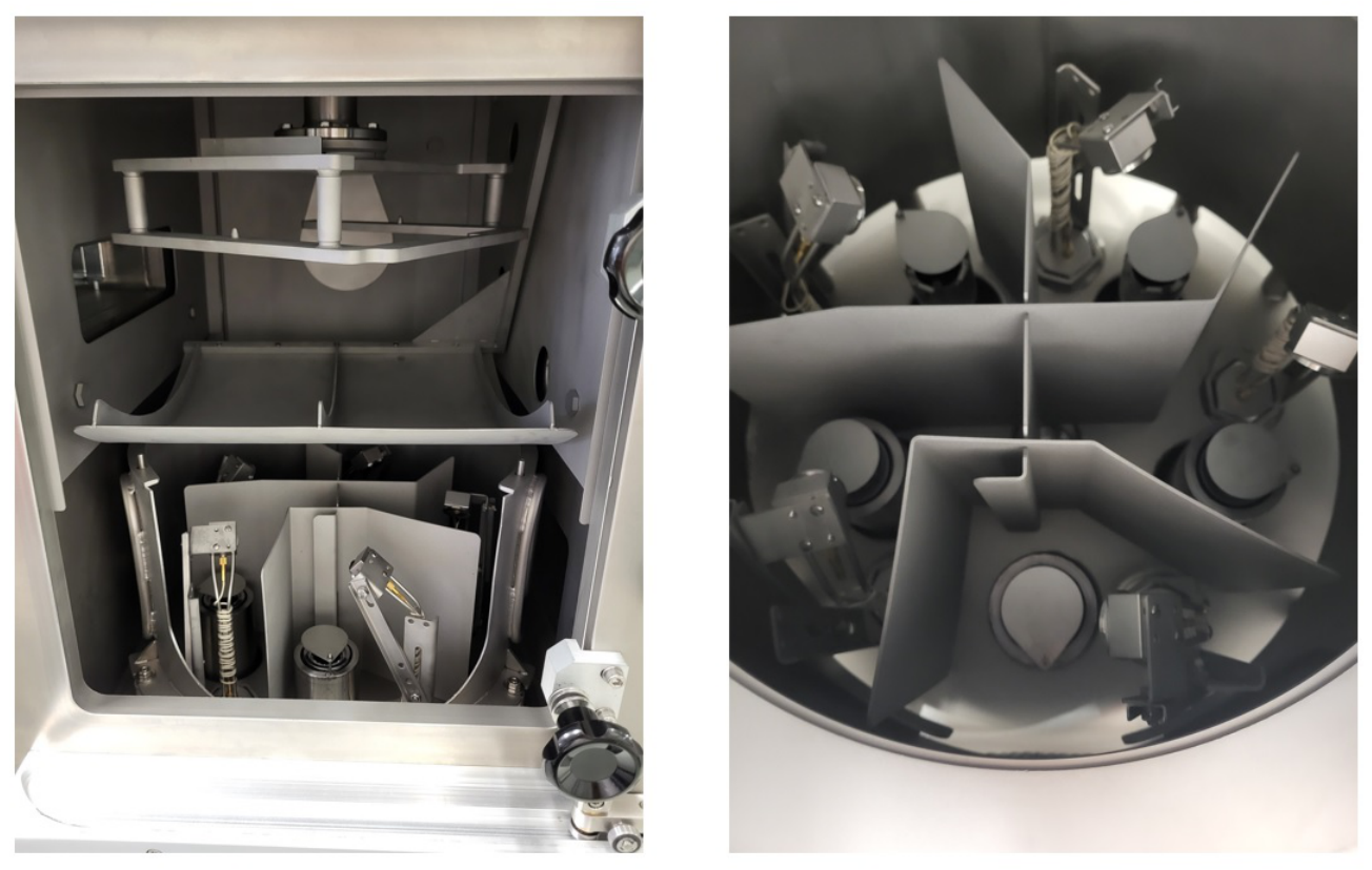
Figure 2.
XRD patterns of evaporated Cu films with nominal thicknesses of 40, 100, and 250 nm deposited on glass substrates. The main peaks are indexed to fcc Cu and can be assigned to the (111), (200), and (220) planes.
Figure 2.
XRD patterns of evaporated Cu films with nominal thicknesses of 40, 100, and 250 nm deposited on glass substrates. The main peaks are indexed to fcc Cu and can be assigned to the (111), (200), and (220) planes.
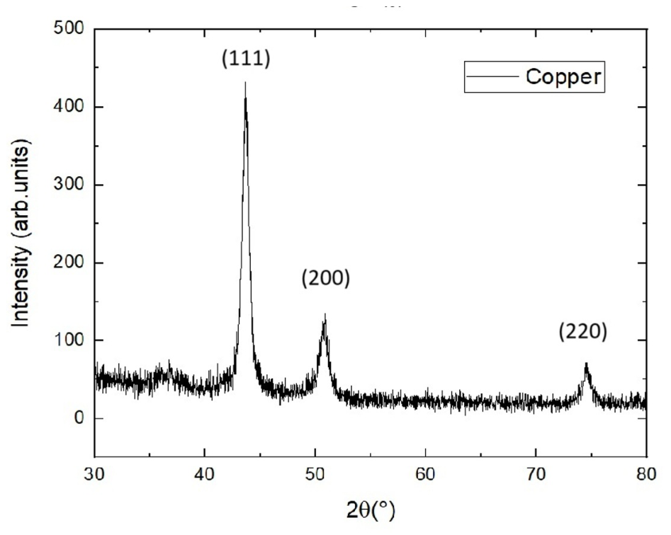
Figure 3.
Representative plan-view SEM micrograph of the evaporated Cu film with nominal thickness of 40 nm, showing a compact nanogranular morphology. Scale bar: 30 nm. Grain size details with enhanced contrast as inset.
Figure 3.
Representative plan-view SEM micrograph of the evaporated Cu film with nominal thickness of 40 nm, showing a compact nanogranular morphology. Scale bar: 30 nm. Grain size details with enhanced contrast as inset.
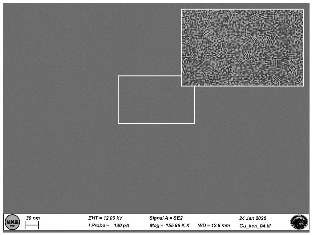
Figure 4.
XPS survey spectrum acquired on the as-deposited Cu film after air exposure, highlighting the main detected elements (Cu, O, and C).
Figure 4.
XPS survey spectrum acquired on the as-deposited Cu film after air exposure, highlighting the main detected elements (Cu, O, and C).
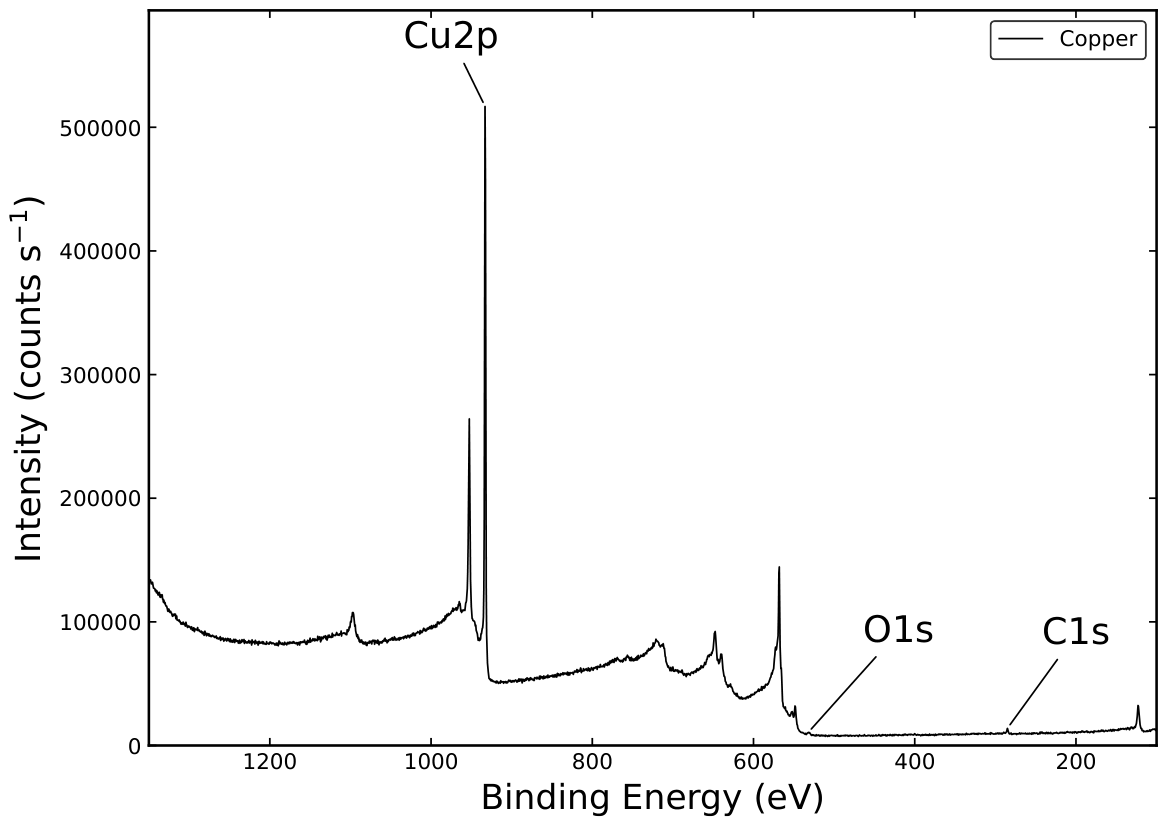
Figure 5.
Optical transmittance spectra of evaporated Cu films with nominal thicknesses of 40, 100, and 250 nm deposited on glass. The transmittance at nm, , was extracted from each curve and used to evaluate the transparent-conductor figure of merit reported in Table 3.
Figure 5.
Optical transmittance spectra of evaporated Cu films with nominal thicknesses of 40, 100, and 250 nm deposited on glass. The transmittance at nm, , was extracted from each curve and used to evaluate the transparent-conductor figure of merit reported in Table 3.
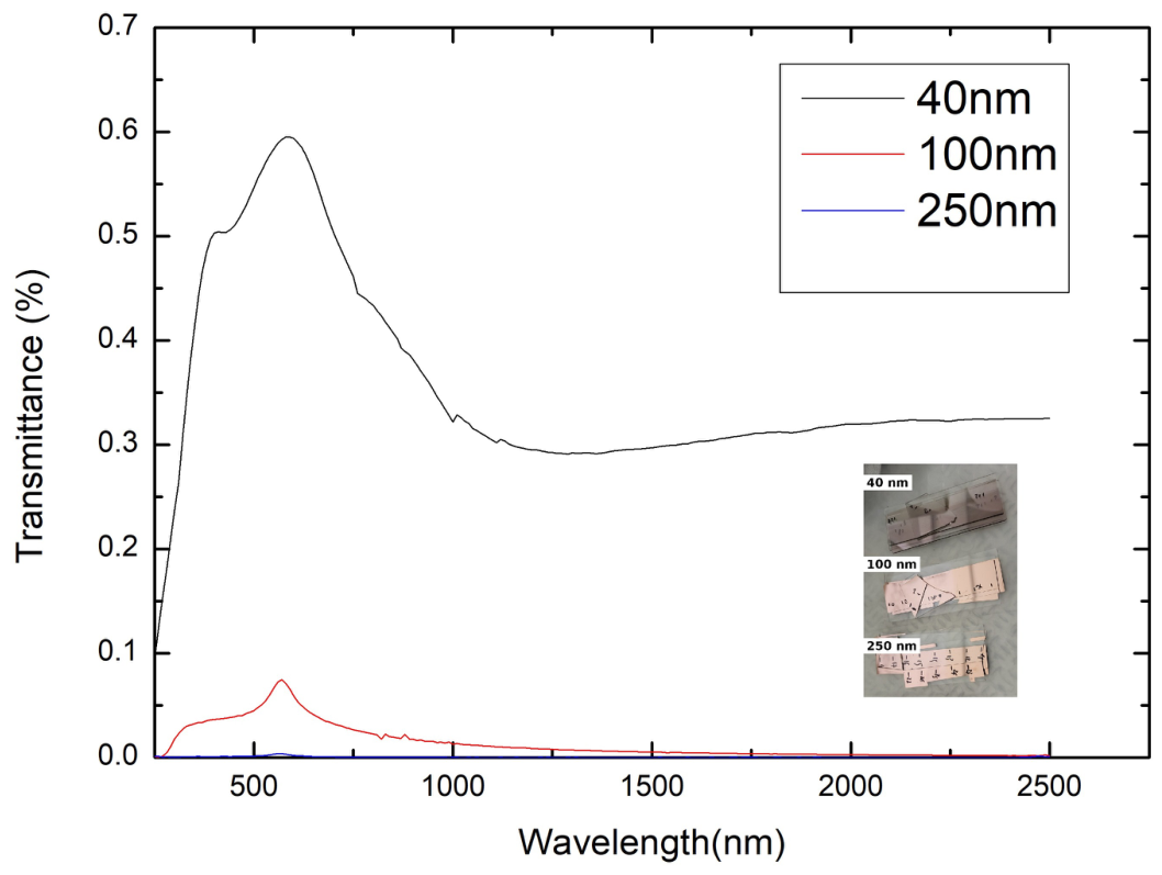
Table 3.
Summary of thickness-dependent optoelectronic properties of evaporated Cu films and corresponding transparent-conductor figure of merit (Haacke), evaluated using T at nm.
Table 3.
Summary of thickness-dependent optoelectronic properties of evaporated Cu films and corresponding transparent-conductor figure of merit (Haacke), evaluated using T at nm.
| Thickness (nm) | () | (%) | () | |
|---|---|---|---|---|
| 40 | 30.0 | 0.58526 | 58.526 | |
| 100 | 1.5 | 0.06693 | 6.693 | |
| 250 | 0.5 | 0.00297 | 0.297 |
Disclaimer/Publisher’s Note: The statements, opinions and data contained in all publications are solely those of the individual author(s) and contributor(s) and not of MDPI and/or the editor(s). MDPI and/or the editor(s) disclaim responsibility for any injury to people or property resulting from any ideas, methods, instructions or products referred to in the content. |
© 2026 by the authors. Licensee MDPI, Basel, Switzerland. This article is an open access article distributed under the terms and conditions of the Creative Commons Attribution (CC BY) license (http://creativecommons.org/licenses/by/4.0/).
Copyright: This open access article is published under a Creative Commons CC BY 4.0 license, which permit the free download, distribution, and reuse, provided that the author and preprint are cited in any reuse.


