

Submitted:
22 June 2026
Posted:
24 June 2026
You are already at the latest version
Abstract
InGaN/GaN quantum wells on polar substrates exhibit a pronounced quan-tum-confined Stark effect, which significantly limits their efficiency as light emitters. Surprisingly, this detrimental effect is significantly reduced when wider wells (above 10 nm) are used; their emission kinetics are the central focus of this work. A time range spanning 9 orders of magnitude, from picoseconds to milliseconds, is explored through various experiments. This includes experiments on the optical visualization of slow decays of charge in the ground states (called “dark charge”) in the millisecond range, experiments on radiative recombination of excited states in the nanosecond range and on the relaxation of hot carriers in the picosecond range. All data are explained within the framework of qualitative and semi-quantitative models. The highly diverse kinet-ics of ground and excited states is due to the fact, that the ground states of electrons and holes have negligible overlap and screen the built-in field, are optically inactive, and recombine nonradiatively in milliseconds. Meanwhile, when the field is screened, the excited states recombine radiatively in the picosecond/nanosecond range. The pulses of photo- and electro-luminescence depend strongly on the excitation period. The application of negative-voltage pulses allows to deplete the well from charge and generates short pulses of light.
Keywords:
wide InGaN quantum wells
; dark charge
; time-resolved photoluminescence and electroluminescence
; InGaN LEDs and LDs
; hot-carrier PL
1. Introduction
It was initially believed [1] that efficient InGaN/GaN emitters (LEDs and LDs) must have narrow (below 4 nm) quantum wells in the active area, since strong electric field in the well (1-2MV/cm) leads to huge Quantum Confined Stark Effect (reduction of the overlap of electron and hole states and red shift of emission energy). Further studies of wide (8-25 nm) quantum well [QW] emitters have shown, that the electric field may be screened by high carrier concentration and efficient LEDs (Light Emitting Diodes) and LDs (Laser Diodes) have been demonstrated [2,3,4,5,6]. It is generally accepted that the emission from wide wells is dominated by excited-state transitions while charge in the ground state screens the built-in field very efficiently. Since this charge does not contribute to emission, it was often called “dark charge”. The screening of electric fields increased the interest in wide-QW structures, since the detrimental effects of built-in fields are hard to eliminate. Alternatives, such as growth on nonpolar substrates resulted in lower structural quality, high doping of the barriers increased nonradiative recombination etc. Another advantage of wide wells is the stability of their emission wavelength with applied bias or varying excitation power.
Dark charge may appear in the well as a result of optical or electrical excitation. However, it looks like even without excitation there is finite concentration of dark charge in the well. The origin of dark charge may be the thermal generation of electrons and holes, followed by their separation by strong electric field, preventing recombination. This would create some concentration of electrons and holes screening the field in the well, increasing nonradiative recombination until generation equals recombination. The extreme situation occurs, when the voltage drop in the well exceeds the bandgap in the well. In that case the Fermi level crosses both the edge of the conduction band and of the valence band, so that electrons and holes appear at the two interfaces of the well.
2. Materials and Methods
The studies which we review were all performed on MBE samples grown on bulk GaN substrates at the Institute of High Pressure Physics in Poland. We shall focus on well widths of 10.4 nm, 15 nm, and 25 nm. Reference samples with narrow (2.6 nm well) have also been grown for comparison. The composition of indium in the wells was 17%. In Figure 1 we show the typical structure of LED and LD with 10-25 nm well. The barriers in LEDs were 20-40 nm wide and contained 2% indium. In case of laser structures the 110 nm barriers contained 4% indium. For LEDs the tunnel junction was grown above the structure, followed by 110 nm n-type cap layer for better electric contacts and current spreading. Metal contacts covered only a fraction of the LED surface, allowing for effective illumination or emission of light.
The experimental setups used for the time-dependent measurements were of three types.
For the picosecond/nanosecond resolution the time-resolved PL system in Max Born Institute has been used with femtosecond 400 nm laser used for excitation (80 MHz frequency), monochromator, and streak camera for PL detection [8,9]. This means that the separation of laser pulses was only 12.5 ns. The resolution of the setup was better than 15 ps. The temperature of the sample was varied from 5K up to 300K.
The system for time resolved electroluminescence in Chemnitz University of Technology used 80-800 ns current pulses for excitation with 20 kHz frequency, monochromator and streak camera for detection of the electroluminescence spectrum [10,11]. The temporal resolution was below 1 ns. The temperature was set to 300K.
In both studies with streak camera the period (frequency) of excitation was fixed.
The third type of time-resolved experiments was based on a photomultiplier with photon counting, having 5 ns resolution. The emission was excited by pulses (from 10 s up to 1 ms) of a 405 nm LD operated CW and passed through acousto-optic modulator (or driven by pulse generator). The detection of emitted light was by a gated photomultiplier attached to the monochromator. The time gate of the photomultiplier was selected between 10 ns up to 1 s, and it was shifted with respect to the excitation pulse to measure the time evolution of the PL emission [12,13,14]. This method allows to vary all parameters: the excitation power, duration, and period. Fast and slow decays (from 100 ns up to seconds) can be measured.
In each case the excitation by 400-405 nm light was resonant, i.e. it generated electrons and holes only in the well.
Another experimental method used to determine (and reduce) the amount of charge in the quantum well was to apply Negative Voltage Pulses (NVPs) [11,12,13,14]. After the excitation pulse (by light or by current) the voltage applied to the diode was switched to negative (reverse) value, reducing the field in the well and facilitating recombination (radiative and nonradiative). These pulses of negative voltage (from 1 s up to 1 ms) were accompanied by Short Pulses of Light (SPLs) with about 10-20 ns duration, as shown in the following.
3. Theoretical background
In order to understand the peculiar properties of wide well emitters it is worth to look at the active layer of these structures as a function of external bias (Figure 2) and of carrier concentrations in the well (achieved by optical or electrical pumping) – Figure 3.
We can see that a negative voltage reduces the field in the well and increases the probability of recombination.
Somewhat different reduction of the field can be achieved by increasing the carrier concentration in the well. The calculations in [10] were based on a 6x6 Hamiltonian for the valence states and the self-consistent solution of the Schrodinger and Poisson equations. The resulting potential profiles of the 10.4 nm and the 25 nm In0.17Ga0.83N/GaN quantum wells are shown in Figure 3 as a function of carrier concentration, together with several eigenstates in the valence and conduction bands.
The wavefunctions plotted in Figure 3 demonstrate the transition from a 2D spectrum in a triangular well (at low carrier concentration) to the almost zero-field 3D spectrum (at high carrier concentration, discussed in [10]. This simulation also demonstrates that the ground states in the well remain spatially separated even when the field is zero in most of the well. This is why they do not contribute to emission but screen the built-in field effectively.
Based on this model the emission spectra have been calculated, also as a function of carrier concentration in the well (Figure 4).
These spectra show huge shifts of the emission lines, from yellow to blue. However, they are normalized and the normalization factors are not shown. In fact, such shifts have never been experimentally observed in wide wells. On the contrary, we already mentioned the stability of the emission energy as a function of excitation power. This stability, however, is seen only at high carrier concentrations. The emission at low concentrations is simply not observable.
Another calculation interpreting the stability of emission wavelength (with current) in wide wells was presented in [15], where it was shown that the stable emission energy occurs at nonzero electric field in the well, but different pairs of excited states contribute to emission, keeping the average energy constant (Figure 5), even when the field is varying.
The intensity of the interband transitions depends on the overlap of the electron and hole wavefunctions, and on the occupation of the two states involved. An important factor is the sensitivity of the detector i.e. what is the threshold intensity observable. The transitions shown for low carrier concentrations in Figure 4 have never been observed. It is difficult to compare the results in Figure 4 and Figure 5 since the former is as a function of concentration and the latter as a function of current density.
4. Experimental Results
4.1. Emission from Wide Wells in the Picosecond/Nanosecond Range
In Refs [8,9] the time-resolved PL spectra from the 25 nm well have been measured from 5K up to 300K (Figure 6).
The above spectra cover approximately one nanosecond range, and the signal below t=0 comes from the previous pulse (12.5 ns before the current pulse).
Some analysis of the wavelength-resolved 5K spectra is shown in Figure 7. The main conclusions of this data can be summarized as follows:
a) wide QW structures show an almost exponential ns-kinetics (Figure 7b, dotted line) and behave like dominated by radiative recombination (since decay times increase with temperature)
b) at low excitation densities the dark charge forms first. This leads to the appearance of a threshold of the PL (and PL) due to excited states (Figure 7d).
c) a very broad spectrum of time constants (from ps to ns) is found when PL is spectrally resolved. At low temperatures, PL decays as fast as 16 ps were found. This PL is assigned to hot carrier PL within the bulklike quasi-continuum of states. At low temperature the carriers photogenerated high in the bands recombine mainly through interactions with acoustic phonons, which is a fairly slow process. This is why interband transitions at higher energies are possible. At higher temperatures the tails of the Fermi distribution allow for the recombination with the emission of optical phonons, which is very fast. Therefore, the “phonon bottleneck” seems to be the reason for the observation of higher-energy transitions at low temperature.
4.2. Electroluminescence from Wide Wells in the Nanosecond Range
In Ref.[10] the electroluminescence emission from wide wells (10.4 and 25 nm) has been studied using 80 ns current pulses of varying current density j (Figure 8)
Similar results have been obtained for the 25 nm well. The emission starts with some delay with respect to the excitation pulse. This delay decreases with increasing current density, which is consistent with the requirement of a sufficient concentration of dark charge filling the ground states and screening the built-in field. For low current densities the emission shows a low-intensity (50 times lower) peak at 470 nm and for higher densities it saturates at 455 nm. In CW experiments such longer wavelength emission at low excitation has not been observed [16].
Using the same experimental setup it was shown in [11] that bright emission occurs at the trailing edge of the excitation pulse, if the voltage is rapidly switched from positive (3.3V) to negative (reverse) value (Figure 9). In this case the excitation pulse (at 3.3V) was long (800 ns) so as to obtain stationary carrier concentration in the well.
The figure shows the last 100 ns of the pulse. At the end of the pulse we can see a strong increase of emission for the 10.4 nm well, and the appearance of short pulse of light in case of the 25 nm well. This effect has been also observed and studied in more detail in time resolved studies in the microsecond range, described later. In Figure 10 the emission intensity is shown vs. time. These short pulses appear due to the reduction of the electric field by reverse bias, so that the charge trapped in the well recombines through excited states (due to rapid transfer of dark charge to excited states).
These short pulses were observed in laser structures so there was a discussion in [14] if they could be made strong enough to generate lasing.
We shall now review some time-dependent studies in the microsecond (and above) range showing very slow decay and “regeneration” effects of dark charge.
4.3. PL Emission from Wide Wells in the Microsecond Range
The evidence for the existence of dark charge was supplied by the study of PL emission excited by 10-30 ms pulses of 405 nm LD in 15 and 25 nm wells [12]. It was found that the shape and intensity of PL emission was dependent on the temporal separation (fill factor) of exciting pulses (Figure 11). In narrow quantum wells the PL emission decays in nanoseconds and the separation of the pulses does not matter.
In [12] a simple model of PL emission from two coupled states explained some of the observed features but also predicted slow decay of PL pulses, contrary to the experiment.
A more detailed study of PL pulses as a function of their separation was performed in [13]. In addition, negative voltage pulses (NVPs) were applied after the laser pulses, reducing the dark charge concentration. The periodic excitation without NVPs revealed a monotonic decrease of PL pulses when their separation was increased, up to about 30 ms. Above 30 ms the intensity and shape of the PL pulses stabilized (Figure 12a). This reflects slow decay of dark charge.
When the NVPs were applied 3 ms after the laser pulse (-10V for 10 s) the intensity of PL pulses increased with increasing separation of PL pulses (Figure 12b). This effect (called “regeneration of dark charge”) demonstrated, that after depleting the well from dark charge, its concentration slowly increases with time and saturates at around 30 ms. This implies that there is some equilibrium population of „dark charge” in wide well. This charge is present in the QW without any excitation. If we reduce the population of „dark charge” (by NVP) below this equilibrium value, it will increase (or “regenerate”) towards the equilibrium population within tens of milliseconds. In Figure 12c the integral of PL pulses is shown as a function of excitation period. It looks that the decay curve and the regeneration curve tend to the same limit. The initial changes (up to about 1 ms) are much faster than those above 1 ms.
The NVPs applied after the laser pulse lead to the appearance of SPLs (Short Pulses of Light), as discussed before. Those SPLs can be observed up to 100 s after the laser pulse (Figure 13b). The SPLs are indeed short (10 ns) but the effect of NVPs on PL pulses persists up to its duration of 10 s or more (Figure 13a). After the application of negative voltage the electric field is reduced in the well and some dark charge is “promoted” to excited states. That gives a short pulse of emission, followed by slower nonradiative decay of dark charge. In the following it will be shown that the decay of dark charge during the NVP may be observed for milliseconds.
Similar effects were observed for a 25 nm well. Another demonstration of the NVPs reducing the dark charge was obtained by fixing the excitation period at 30 ms, and varying the position of NVP (Figure 14).
The data in Figure 12, Figure 13 andFigure 14 were obtained for the diode at V=0 (closed circuit). When the reverse bias was applied to the diode, the PL pulses increased, but the effects of delay and regeneration (changes with excitation period) decreased. This is due to the fact, that reverse bias lowers the field in the well and the effect of NVPs (switching to -10V) is reduced.
Figure 15.
Integrated PL intensity for LED with 15 nm well (a) and for LED with 25 nm well (b) as a function of excitation period (for different CW voltages from 0V down to -5V). The excitation was with 405 nm, 3 mW, 30 s laser pulses in (a) and 10 s pulses in (b). Solid lines show the decay of PL pulses with increasing separation. Dashed lines show the regeneration of the PL signal after the application of NVP with 10 s duration and -10V voltage. The NVP was applied 3 s after the laser excitation pulse. (reprinted with permission from [13]).
Figure 15.
Integrated PL intensity for LED with 15 nm well (a) and for LED with 25 nm well (b) as a function of excitation period (for different CW voltages from 0V down to -5V). The excitation was with 405 nm, 3 mW, 30 s laser pulses in (a) and 10 s pulses in (b). Solid lines show the decay of PL pulses with increasing separation. Dashed lines show the regeneration of the PL signal after the application of NVP with 10 s duration and -10V voltage. The NVP was applied 3 s after the laser excitation pulse. (reprinted with permission from [13]).
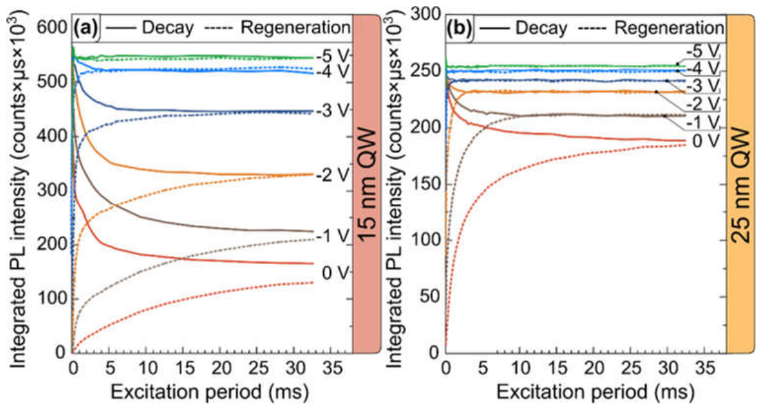
Figure 16.
Examples of fits of PL decay (a) and regeneration (b) for LED with 25 nm well at V=-1V. The data below 1 ms (fitted with blue line) show fast decay/regeneration, while the data above 1 ms (fitted with red line) show much slower variation, (c) lifetime of “dark charge” vs reverse voltage obtained from the fits for the 25 nm well. (reprinted with permission from [13]).
Figure 16.
Examples of fits of PL decay (a) and regeneration (b) for LED with 25 nm well at V=-1V. The data below 1 ms (fitted with blue line) show fast decay/regeneration, while the data above 1 ms (fitted with red line) show much slower variation, (c) lifetime of “dark charge” vs reverse voltage obtained from the fits for the 25 nm well. (reprinted with permission from [13]).
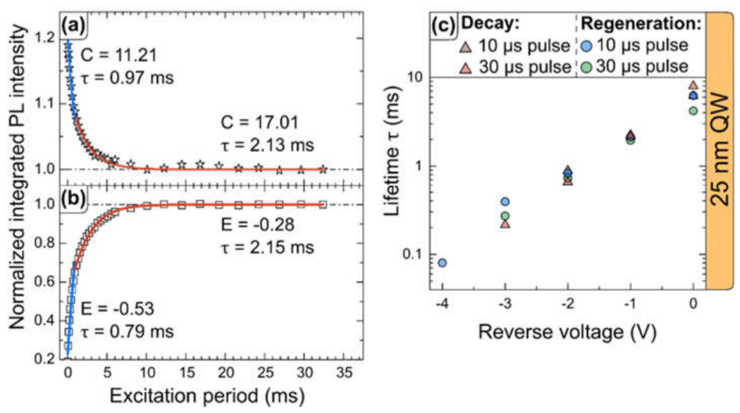
A simple kinetic model with exponential decay and regeneration of dark charge was presented in [13]. However, since during the first 0.5-1 ms the decay/regeneration is fast and it slows down for longer times, it was necessary to fit the data in two regions: up to 1 ms and above 1 ms. The decay/regeneration times obtained from the fits (in the range above 1 ms) for the 15 nm well sample are shown in Figure 13 (c) as a function of reverse voltage. The scatter of values for is large, but the strong reduction with voltage is clear. The decay and regeneration times have similar values.
Long lifetimes of dark charge may be attractive for charge-coupled or memory devices where information is stored in long-lived carrier populations.
4.4. Electroluminescence from Wide Wells in the Microsecond Range
Pulses of positive voltage (current) in the 800 ns range, followed by negative voltage, resulted in SPLs at the trailing edge of the pulse, as shown in [11]. The separation of the excitation pulses (and their duration) was fixed in these experiments. Using the photomultiplier for detection and a pulse generator for excitation, it was possible to perform a similar experiment using NVPs ([14]). All parameters could be varied in a wide range; duration of NVPs, period of NVPs, and voltages. The experiment consisted in driving the diode with low CW positive voltage (below the threshold for emission, typically 1-3V) and applying periodically NVPs. Depending on the period of NVPs and on the value of the positive voltage, the diode started to emit SPLs at the beginning (leading edge) of each negative voltage pulse. There was no emission in-between the NVPs (Figure 17). This experiment is somewhat similar to the regeneration of PL in [13].
The NVPs deplete the QW from dark charge (partially or completely, depending on their voltage and duration). If their separation is short, dark charge does not recover sufficiently till the next NVP and the emission (SPL) is absent. If the separation of NVPs is long enough and the current pumping the well is sufficient, the emission appears at the beginning (leading edge) of each NVP.
The dependence of the integrated intensity of SPLs on the positive voltage and on the period of NVPs is shown in Figure 18 (for the LED with 25 nm well). The separation between subsequent NVPs is increased (from 10s up to 10ms) so that the charging time of the well is increased. The integrated intensity of SPLs is shown as a function of this separation (for several forward voltages), see Figure 18(a). For low voltages up to 1.25V there is no measurable emission from the sample. At 1.4V the SPLs start to appear if the separation of NVPs (charging time) is above 1ms. For increasing voltage (current) this “threshold separation” is reduced. Above the “threshold separation” the intensity of SPLs increases and saturates. The saturation intensity of SPLs increases with forward voltage (current).
Similar experiments performed for lower NVP voltages (-5V and -3V) showed lower intensity of SPLs and longer charging times required for their appearance (Figure 18b,c).
Increasing the duration of NVPs (from 100 ns up to 1 ms) requires longer charging times for the SPLs to appear (Figure 19). This means that during the NVP there is nonradiative recombination of dark charge for a much longer time than the duration of SPLs (10 ns). The duration of NVP to achieve maximum depletion of the well from dark charge depends on the negative voltage of NVP; for -10V it is about 1-10 s, for -5V around 100 s, and for -3V it is longer than 1 ms.
5. Numerical Simulation of Transient Electroluminescence
In Refs [14,17] a transient one-dimensional drift-diffusion model has been used to simulate the time-dependent evolution of emission from a 25 nm well, subject to periodic NVPs. In Figure 20 the band profiles of the active layer of the diode are shown at four steps of the experimental procedure.
At moment t1 (right after NVP, at positive voltage of 2.75V) the well contains very little charge, located close to its edges. Both wavefunctions (of ground and excited states) for electrons and holes show negligible overlap. It is important to note that the well is not in equilibrium, because the carriers were depleted during the NVP. Therefore, during the time between t1 and t2 the well is charged by low intensity current and the field becomes partly screened. The inflow of carriers is balanced by nonradiative recombination (Shockley-Read-Hall). The total current densities of electrons and holes approach each other but there is still no detectable emission from the well. Now, when we apply negative voltage of -10V (moment t3) the field in the well is rapidly reduced (we assume that the switch of voltage is much shorter than the recombination time of carriers). The wavefunctions of electrons and holes spread into the well, but the ground states still have very small overlap compared to excited states. The excited states with high overlap generate short emission pulses (SPLs) followed by some nonradiative recombination. The recombination during the NVP leads to reduced charge density (and increased electric field) at moment t4. The charge density remaining in the QW depends on the duration of the NVP.
The accumulation of dark charge after the NVP (moment t1) under positive bias until the next NVP (moment t2) calculated in [14] is shown in Figure 21.
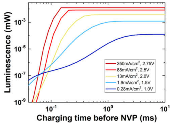
Finally, the dependence of emission peaks (SPLs) on the charging time before NVP has been calculated (Figure 22). The structure is initially set in the depleted-charge state, then the transient simulation starts with low forward bias imposed, which is not sufficient to turn-on the normal LED operation. After some time, which is varied from 0.1ms up to 10ms, the -10V NVP is applied for 10 µs, then the forward bias is restored for a short time and simulation ends. The results agree qualitatively with the experimental data, shown in Figure 18. In theory the emission is always present (though at extremely low levels), while in experiment it appears at some threshold level, depending on the sensitivity of the detector.
6. Summary and Conclusions
The transient properties of wide InGaN QWs in different time domains reveal some specific effects not encountered in regular, i.e. narrow wells. In picosecond TRPL experiments, fast radiative recombination from a hot-carrier plasma has been observed at low temperatures. The power dependence of emission showed a threshold behavior, attributed to the presence of dark charge. Electroluminescence in the nanosecond range showed a delay of emission with respect to the current pulse, decreasing with increasing current. Fast switching from positive to negative voltage revealed SPLs (with about 10 ns duration).
In these experiments the period of excitation was fixed. In the experiments using gated photomultiplier in the microsecond range both PL and EL pulses have been studied as a function of their separation. The presence of dark charge caused a decay of PL (or EL) pulses while increasing their separation up to 30 ms. The application of NVPs allowed to decrease the population of dark charge, generating SPLs at the beginning of the pulse, and slow recovery of dark charge population until the next NVP.
Electroluminescence studies with the application of NVPs determined the conditions for the appearance of SPLs, in agreement with numerical simulation. The duration of NVPs up to 1 ms affected the appearance and intensity of SPLs, showing the slow recombination of dark charge due to nonradiative transitions (Shockley-Read-Hall). The possibility of achieving lasing during SPLs remains an open question.
The effective screening of built-in field by dark charge (allowing for the emission between excited states) and the stability of emission energy make wide well LEDs and LDs worth further research. Long lifetime of dark charge could be interesting for charge-coupled or memory devices. And, above all, wide InGaN quantum wells provide new interesting physical effects.
Author Contributions
For research articles with several authors, a short paragraph specifying their individual contributions must be provided. The following statements should be used “Conceptualization, W.T. and A.B.; methodology, A.B. and J.T.; software, K.S.; validation, J.T., G.M. and M.H.; investigation, A.B. and J.T.; resources, G.M. and M.H.; data curation, K.S.; writing—original draft preparation, W.T.; writing—review and editing, W.T. and J.T.; visualization, M.H.; supervision, W.T.; All authors have read and agreed to the published version of the manuscript.”
Funding
Please add: “This research received no external funding”
Institutional Review Board Statement
“Not applicable”
Data Availability Statement
This is a review so no new data were created.
Conflicts of Interest
“The authors declare no conflicts of interest.”
References
- Bai, J.; Wang, T.; Sakai, S. “Influence of the quantum-well thickness on the radiative recombination of InGaN/GaN quantum well structures”. J. Appl. Phys. 2000, 88, 4729–4733. [Google Scholar] [CrossRef]
- Gardner, N. F.; Müller, G. O.; Shen, Y. C.; Chen, G.; Watanabe, S.; Götz, W.; Krames, M. R. “Blue-emitting InGaN–GaN double-heterostructure light-emitting diodes reaching maximum quantum efficiency above 200 A/cm2”. Appl. Phys. Lett. 2007, 91, 243506. [Google Scholar] [CrossRef]
- Maier, Markus; Köhler, Klaus; Kunzer, Michael; Pletschen, Wilfried; Wagner, Joachim. “Reduced nonthermal rollover of wide-well GaInN light emitting diodes”. Appl. Phys. Lett. 2009, 94, 041103. [Google Scholar] [CrossRef]
- Laubsch, Ansgar; Bergbauer, Werner; Sabathil, Matthias; Strassburg, Martin; Lugauer, Hans; Peter, Matthias; Meyer, Tobias; Brüderl, Georg; Wagner, Joachim; Linder, Norbert; Streubel, Klaus; Hahn, Berthold. Luminescence properties of thick InGaN quantum-wells. Phys. Status Solidi 2009, 6, S885. [Google Scholar] [CrossRef]
- Muziol, Grzegorz; Turski, Henryk; Siekacz, Marcin; Szkudlarek, Krzesimir; Janicki, Lukasz; Baranowski, Michal; Zolud, Sebastian; Kudrawiec, Robert; Suski, Tadeusz; Skierbiszewski, Czeslaw. “Beyond Quantum Efficiency Limitations Originating from the Piezoelectric Polarization in Light-Emitting Devices”. ACS Photonics 2019, 6(8), 1963–1971. [Google Scholar] [CrossRef]
- Muziol, G.; Hajdel, M.; Siekacz, M.; Turski, H.; Pieniak, K.; Bercha, A.; Trzeciakowski, W.; Kudrawiec, R.; Suski, T.; Skierbiszewski, C. “III-nitride optoelectronic devices containing wide quantum wells—unexpectedly efficient light sources”. Jpn. J. Appl. Phys. 2022, 61, SA0801. [Google Scholar] [CrossRef]
- Bercha, A.; Chlipala, M.; Hajdel, M.; Muziol, G.; Siekacz, M.; Muziol, G.; Turski, H.; Trzeciakowski, W. Photoluminescence and Photocurrent from InGaN/GaN Diodes with Quantum Wells of Different Widths and Polarities. Nanomaterials 2025, 15(2). [Google Scholar] [CrossRef] [PubMed]
- Tomm, Jens W.; Bercha, Artem; Muzioł, Grzegorz; Piprek, Joachim; Trzeciakowski, Witold. “Recombination in Polar InGaN/GaN LED Structures with Wide Quantum Wells”. Phys. Status Solidi RRL 2023, 17, 2300027. [Google Scholar] [CrossRef]
- Tomm, Jens W.; Sakowski, Konrad; Bercha, Artem; Muzioł, Grzegorz; Becht, Conny; Schwarz, Ulrich T.; Trzeciakowski, Witold. “Fast non-equilibrium carrier dynamics in polar InGaN/GaN structures with wide quantum wells”. Appl. Phys. Lett. 2025, 126, 161103. [Google Scholar] [CrossRef]
- Uhlig, Lukas; Tepaß, Jannina; Hajdel, Mateusz; Muziol, Grzegorz; Schwarz, Ulrich T. Transition between quantum confinement and bulklike behavior in polar quantum wells. Phys. Rev. B 2023, 108, 045304. [Google Scholar] [CrossRef]
- Tepaß, Jannina; Uhlig, Lukas; Hajdel, Mateusz; Muziol, Grzegorz; Schwarz, Ulrich T. Bright Emission at Reverse Bias After Trailing Edge of Driving Pulse in Wide InGaN Quantum Wells. Phys. Status Solidi A 2023, 220, 2300042. [Google Scholar] [CrossRef]
- Bercha, A.; Trzeciakowski, W.; Muzioł, G.; Tomm, J. W.; Suski, T. “Evidence for “dark charge” from photoluminescence measurements in wide InGaN quantum wells”. Opt. Express 2023, Vol. 31, 3227–3236. [Google Scholar] [CrossRef] [PubMed]
- Bercha, Artem; Muziol, Grzegorz; Chlipala, Mikolaj; Trzeciakowski, Witold. “Long-Lived Excitations in Wide (In,Ga)N/GaN Quantum Wells”. Phys. Rev. Appl. 20, 034040. [CrossRef]
- Bercha, Artem; Sakowski, Konrad; Muziol, Grzegorz; Hajdel, Mateusz; Trzeciakowski, Witold. “Light emission at reverse voltage in a wide-well (In,Ga)N/GaN light-emitting diode”. Phys. Rev. Appl. 2023, 21, 054030. [Google Scholar] [CrossRef]
- Hajdel, Mateusz; Gołyga, Krzysztof; Siekacz, Marcin; Feduniewicz-Żmuda, Anna; Skierbiszewski, Czesław; Schwarz, Ulrich Theodor; Muziol, Grzegorz. “Distinctness of Electroluminescence and Optical Gain in Laser Diodes with Wide Polar Quantum Wells”. ACS Photonics 2025, 12, 1515−1523. [Google Scholar] [CrossRef] [PubMed]
- Hajdel, Mateusz; Chlipała, Mikolaj; Siekacz, Marcin; Turski, Henryk; Wolny, Paweł; Nowakowski-Szkudlarek, Krzesimir; Feduniewicz-Żmuda, Anna; Skierbiszewski, Czeslaw; Muziol, Grzegorz. “Dependence of InGaN QuantumWell Thickness on the Nature of Optical Transitions in LEDs”. Materials 2022, 15, 237. [Google Scholar] [CrossRef] [PubMed]
- Sakowski, Konrad; Bercha, Artem; Muziol, Grzegorz; Hajdel, Mateusz; Trzeciakowski, Witold. “Simulations of Light Emission at Reverse Voltage of Wide-Well InGaN Light-Emitting Diodes”. Conf. Pap. NUSOD 2025. [Google Scholar] [CrossRef]
Figure 1.
Structure of the typical wide-well LED sample (a) and LD sample (b). QW thicknesses were dQW=10.4, 15, or 25 nm (adapted with permission from [12] © Optica Publishing Group).
Figure 1.
Structure of the typical wide-well LED sample (a) and LD sample (b). QW thicknesses were dQW=10.4, 15, or 25 nm (adapted with permission from [12] © Optica Publishing Group).
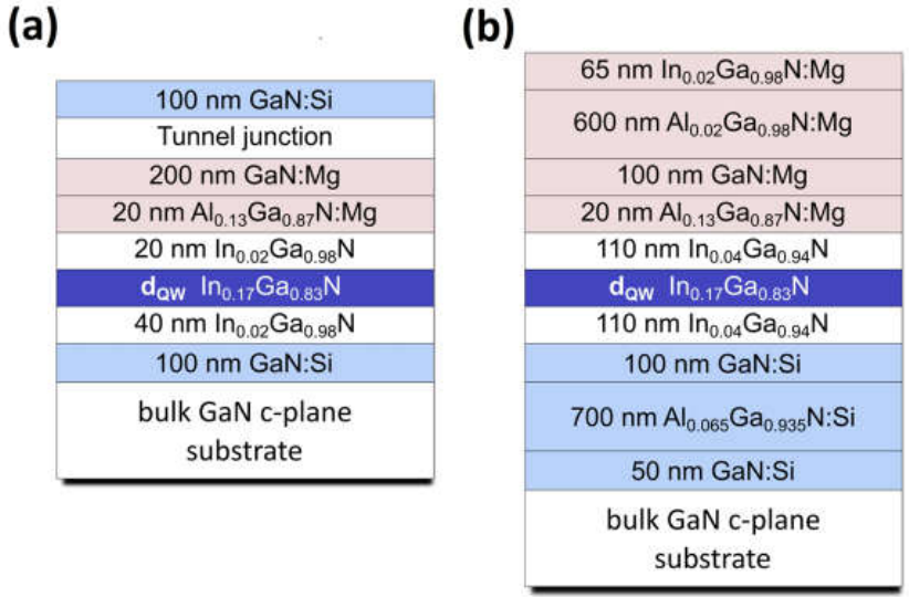
Figure 2.
Potential profile of a LED with 25-nm well at zero voltage (a) and at −10-V reverse voltage (b). Quasi-Fermi levels are marked by dotted lines; solid blue lines show the electric field profile. In (a), the Fermi level crosses the edges of the quantum well, which means that, at zero voltage, both electrons and holes are present in the well without any external excitation. This is not the case at −10 V (b) (reprinted with permission from [13]).
Figure 2.
Potential profile of a LED with 25-nm well at zero voltage (a) and at −10-V reverse voltage (b). Quasi-Fermi levels are marked by dotted lines; solid blue lines show the electric field profile. In (a), the Fermi level crosses the edges of the quantum well, which means that, at zero voltage, both electrons and holes are present in the well without any external excitation. This is not the case at −10 V (b) (reprinted with permission from [13]).
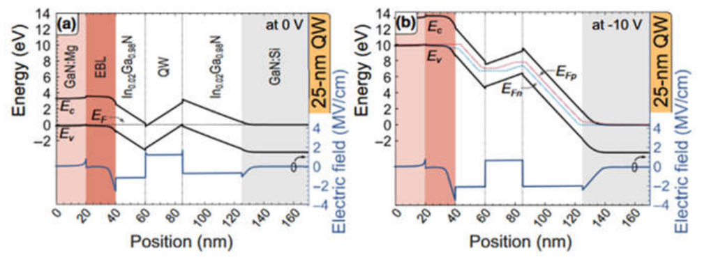
Figure 3.
Potential, squared wave functions and energy states for conduction and valence bands in (a) 10.4-nm and (b) 25-nm-wide QWs, shown for different charge carrier densities N. The orange lines show conduction band electron wave functions, whereas the heavy hole, light hole, and crystal-field split-off states are drawn in red, green, and blue, respectively. For clarity, only the three lowest states of each type are shown. Heavy- and light-hole wave functions are almost identical (green lines hide red lines), whereas the split-off states are barely involved in recombination. (reprinted with permission from [10]).
Figure 3.
Potential, squared wave functions and energy states for conduction and valence bands in (a) 10.4-nm and (b) 25-nm-wide QWs, shown for different charge carrier densities N. The orange lines show conduction band electron wave functions, whereas the heavy hole, light hole, and crystal-field split-off states are drawn in red, green, and blue, respectively. For clarity, only the three lowest states of each type are shown. Heavy- and light-hole wave functions are almost identical (green lines hide red lines), whereas the split-off states are barely involved in recombination. (reprinted with permission from [10]).
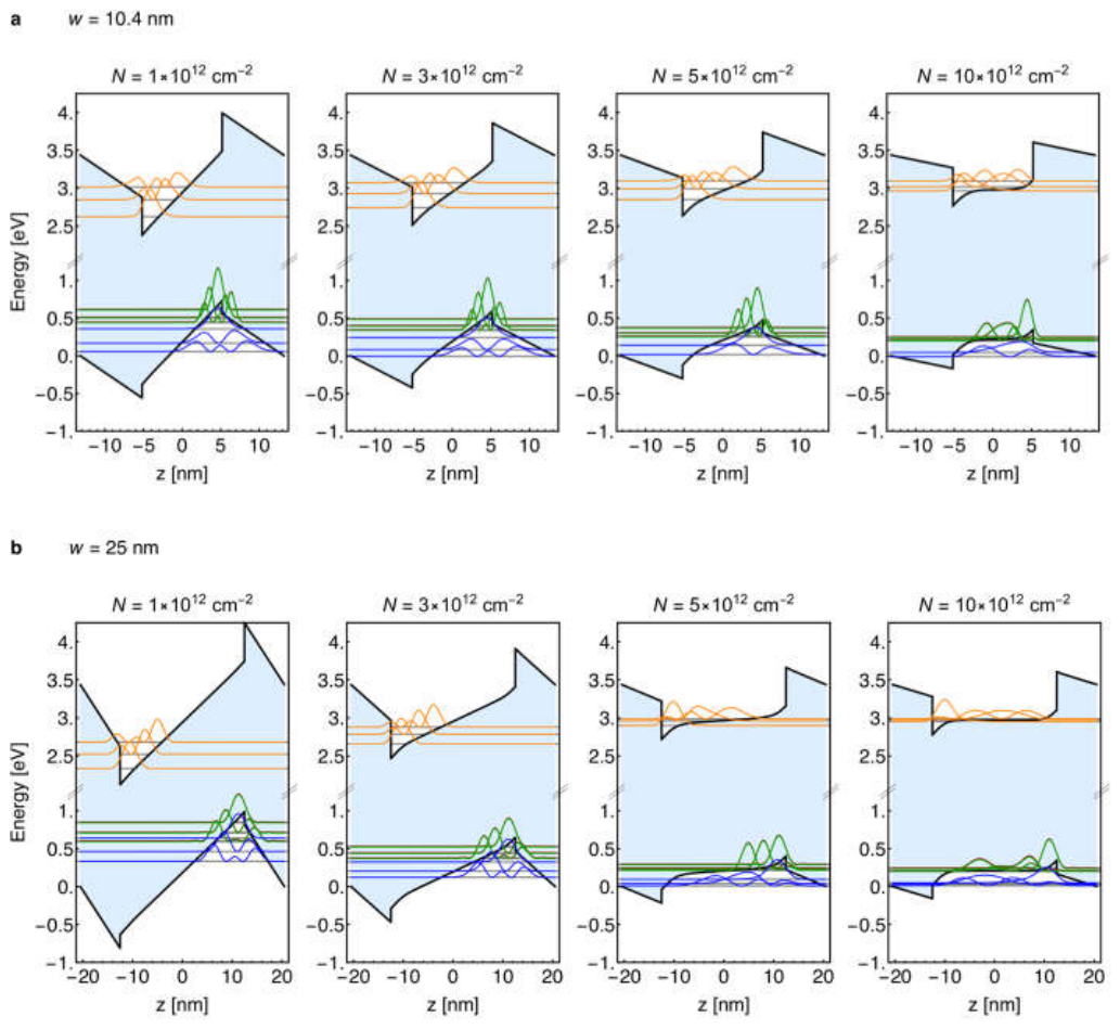
Figure 4.
Normalized spontaneous emission spectra calculated for (a) 10.4-nm- and (b) 25-nm-wide QWs at different carrier densities. ((reprinted with permission from [10]).
Figure 4.
Normalized spontaneous emission spectra calculated for (a) 10.4-nm- and (b) 25-nm-wide QWs at different carrier densities. ((reprinted with permission from [10]).
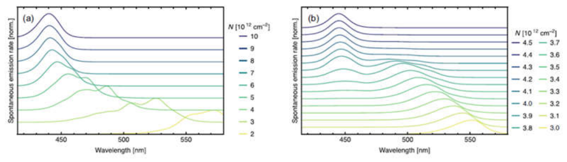
Figure 5.
Simulated band structure of a 25 nm wide QW at (a) j = 1 A cm−2 and (b) j = 1000 A cm−2 with wave functions of the first seven heavy hole and four electron levels. Energy values are indicated by base lines, and wave functions are normalized and scaled for better visibility. (c) Calculated dependence of partial intensity of the most important transitions on current density. (d) Dependence of transition energies for transitions presented in (c) on current density. The color scale represents the contribution to total intensity and is identical to that in panel (c). (e) Dependence of the electric field in the middle of the 25 nm wide QW on current density. The dashed vertical lines in panels (c), (d), and (e) indicate the excitation levels, which correspond to band structures shown in panels (a) and (b). (reprinted with permission from [15]).
Figure 5.
Simulated band structure of a 25 nm wide QW at (a) j = 1 A cm−2 and (b) j = 1000 A cm−2 with wave functions of the first seven heavy hole and four electron levels. Energy values are indicated by base lines, and wave functions are normalized and scaled for better visibility. (c) Calculated dependence of partial intensity of the most important transitions on current density. (d) Dependence of transition energies for transitions presented in (c) on current density. The color scale represents the contribution to total intensity and is identical to that in panel (c). (e) Dependence of the electric field in the middle of the 25 nm wide QW on current density. The dashed vertical lines in panels (c), (d), and (e) indicate the excitation levels, which correspond to band structures shown in panels (a) and (b). (reprinted with permission from [15]).
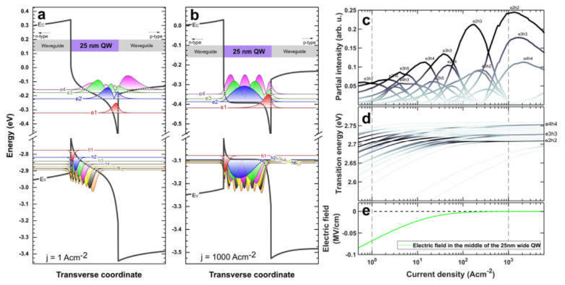
Figure 6.
(a)–(f) Normalized transient PL spectra from the 25 nm QW sample recorded at (a) and (b) T=5 K, (c) and (d) T=80 K, and (e) and (f) T=300 K for an excitation of 1011 carrier pairs per pulse and cm2 with 400-nm photons. While (a), (c), (e) show spectra time-averaged over the entire 12.5-ns period between two excitation pulses as full lines, (b), (d), (f) display maps of the spectral-temporal behavior during only 1 ns including t=0 (position of the excitation pulse that is not shown) and the initial 850 ps of the PL decay. The dotted spectrum in (a) is time averaged in the time interval of -200 to -100 ps, i.e., the PL just before the pulse. (reprinted with permission from [9]).
Figure 6.
(a)–(f) Normalized transient PL spectra from the 25 nm QW sample recorded at (a) and (b) T=5 K, (c) and (d) T=80 K, and (e) and (f) T=300 K for an excitation of 1011 carrier pairs per pulse and cm2 with 400-nm photons. While (a), (c), (e) show spectra time-averaged over the entire 12.5-ns period between two excitation pulses as full lines, (b), (d), (f) display maps of the spectral-temporal behavior during only 1 ns including t=0 (position of the excitation pulse that is not shown) and the initial 850 ps of the PL decay. The dotted spectrum in (a) is time averaged in the time interval of -200 to -100 ps, i.e., the PL just before the pulse. (reprinted with permission from [9]).
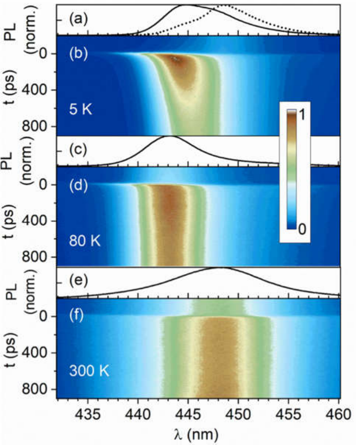
Figure 7.
(a) PL transients at different wavelengths at T=5 K and an excitation of 1011 carrier pairs per pulse and cm-2 taken as vertical cuts from PL maps as shown in Figure 6(b). (b) The same dataset but normalized and in a logarithmic plot. The dotted line represents the wavelength-integrated transient. (c) The same as (b) on a shorter timescale. The gray bar visualizes the time resolution. The color code of the temperatures in the top panel applies to (a)–(c). (d) Power dependences of the PL signal averaged in time over the full 12.5 ns period between two excitation pulses (black) and wavelength-integrated PL taken in the 200–650 ps time window (red) at T=5 K. The dotted line marks the threshold excitation. (reprinted with permission from [9]).
Figure 7.
(a) PL transients at different wavelengths at T=5 K and an excitation of 1011 carrier pairs per pulse and cm-2 taken as vertical cuts from PL maps as shown in Figure 6(b). (b) The same dataset but normalized and in a logarithmic plot. The dotted line represents the wavelength-integrated transient. (c) The same as (b) on a shorter timescale. The gray bar visualizes the time resolution. The color code of the temperatures in the top panel applies to (a)–(c). (d) Power dependences of the PL signal averaged in time over the full 12.5 ns period between two excitation pulses (black) and wavelength-integrated PL taken in the 200–650 ps time window (red) at T=5 K. The dotted line marks the threshold excitation. (reprinted with permission from [9]).
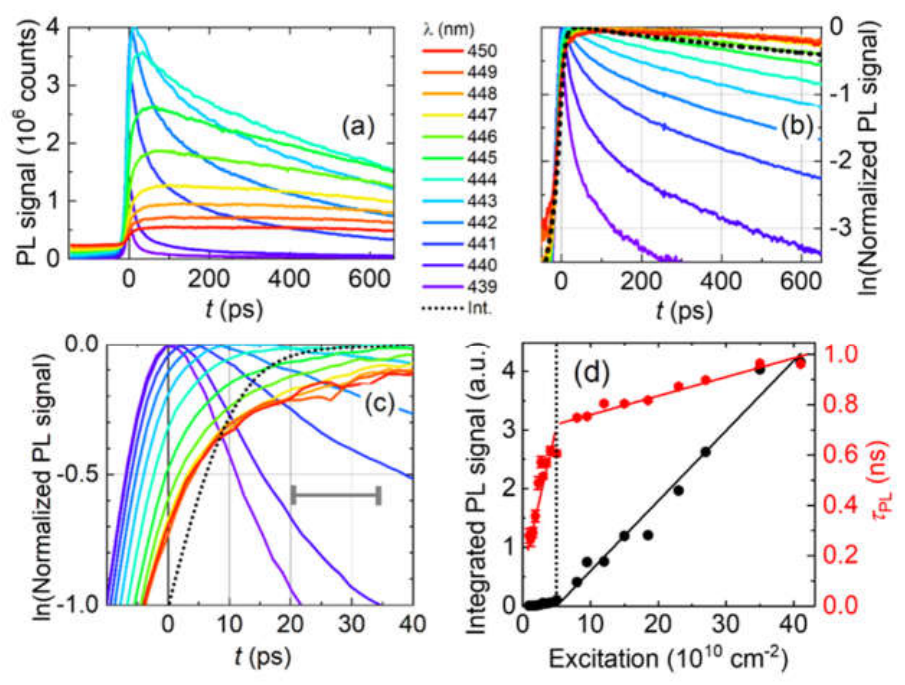
Figure 8.
Streak camera measurements on the 10.4-nm-thick QW. (a)–(d) Spectral-temporal dynamics and (e) time-integrated normalized spectra for different pulse currents. The 80-ns-long driving pulse starts at t = 0 ns. Images (a) and (b) have been measured using photon counting and (c) and (d) in analog integration mode. (reprinted with permission from [10]).
Figure 8.
Streak camera measurements on the 10.4-nm-thick QW. (a)–(d) Spectral-temporal dynamics and (e) time-integrated normalized spectra for different pulse currents. The 80-ns-long driving pulse starts at t = 0 ns. Images (a) and (b) have been measured using photon counting and (c) and (d) in analog integration mode. (reprinted with permission from [10]).
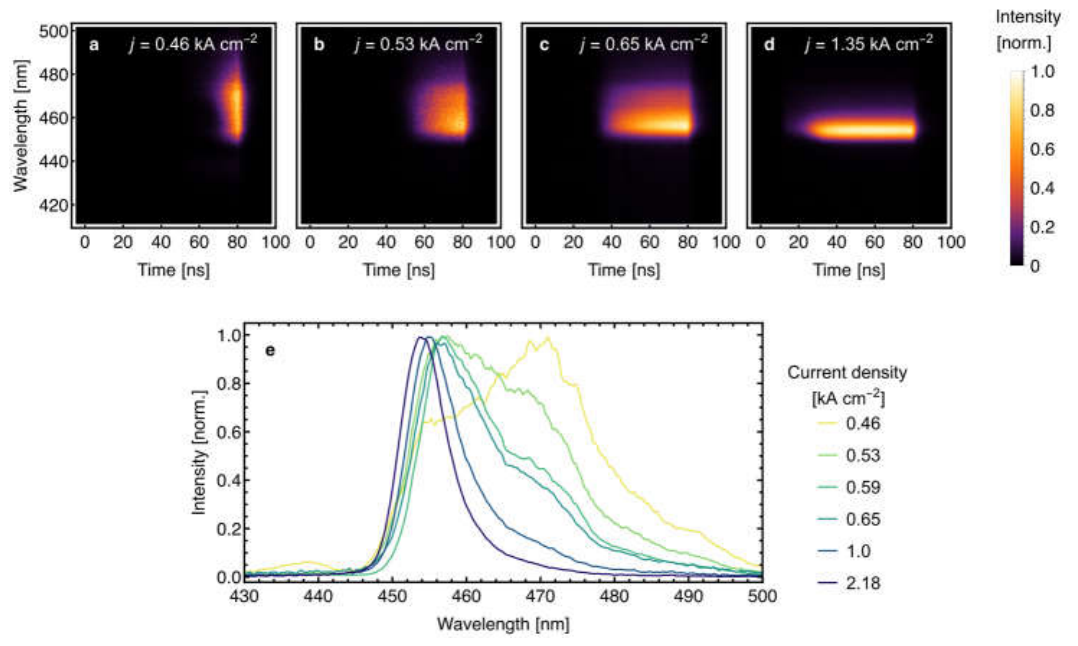
Figure 9.
Streak camera images for the measurement on a laser diode with a 10.4 nm wide QW (left) and a 25 nm wide QW (right). The values of negative bias are shown. (reprinted with permission from [11]).
Figure 9.
Streak camera images for the measurement on a laser diode with a 10.4 nm wide QW (left) and a 25 nm wide QW (right). The values of negative bias are shown. (reprinted with permission from [11]).
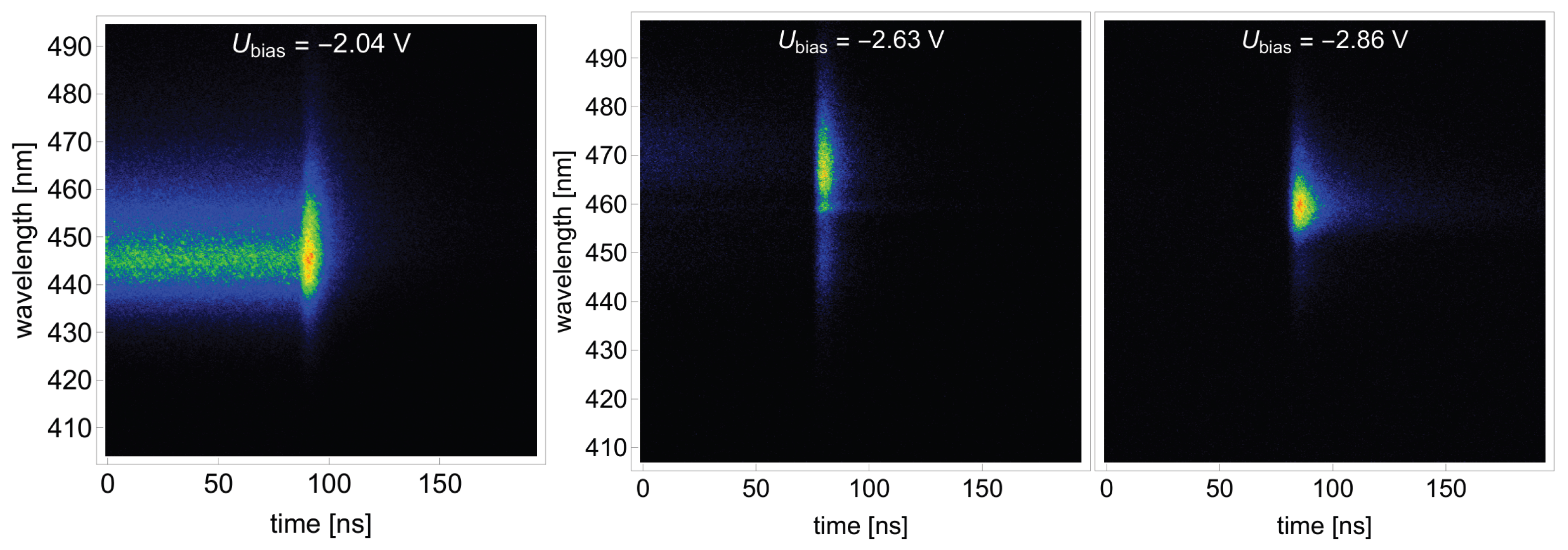
Figure 10.
Time dependence of EL intensity for several values of applied reverse bias for 10.4 nm (left) and 25 nm wide QW(right). The values of negative bias are shown. (reprinted with permission from [11]).
Figure 10.
Time dependence of EL intensity for several values of applied reverse bias for 10.4 nm (left) and 25 nm wide QW(right). The values of negative bias are shown. (reprinted with permission from [11]).
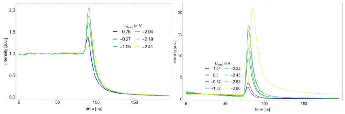
Figure 11.
The effect of different spacing (fill factor) of 30 μs pulses (15 nm well, spacing from 3.3 μs to 29970 μs) for excitation power of 7 mW. (Reprinted with permission from [12] © Optica Publishing Group).
Figure 11.
The effect of different spacing (fill factor) of 30 μs pulses (15 nm well, spacing from 3.3 μs to 29970 μs) for excitation power of 7 mW. (Reprinted with permission from [12] © Optica Publishing Group).
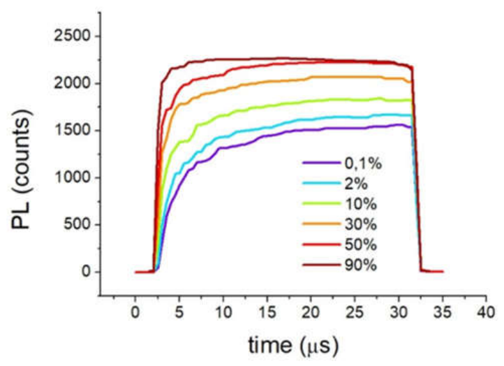
Figure 12.
PL pulses from LED with 15 nm well (excited by 3-mW 30-μs pulses of 405-nm LD) as a function of excitation period (from 50 μs to 32.65 ms) (a) without NVP, (b) with NVP (−10 V, 10-μs duration) applied 3 μs after the laser pulse; (c) integrated intensity of PL shown in (a) and (b).(reprinted with permission from [13]).
Figure 12.
PL pulses from LED with 15 nm well (excited by 3-mW 30-μs pulses of 405-nm LD) as a function of excitation period (from 50 μs to 32.65 ms) (a) without NVP, (b) with NVP (−10 V, 10-μs duration) applied 3 μs after the laser pulse; (c) integrated intensity of PL shown in (a) and (b).(reprinted with permission from [13]).
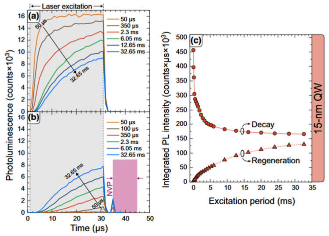
Figure 13.
PL pulses excited by 3 mW, 30 s pulses of the 405 nm LD (10% fill factor): (a) as a function of duration of NVP applied 3 s after the laser pulse (duration of NVP increases from 0 to 10 s), (b) as a function of delay of 1 s NVP with respect to the laser pulse (NVP applied at increasing time delay after the excitation pulse). (reprinted with permission from [13]).
Figure 13.
PL pulses excited by 3 mW, 30 s pulses of the 405 nm LD (10% fill factor): (a) as a function of duration of NVP applied 3 s after the laser pulse (duration of NVP increases from 0 to 10 s), (b) as a function of delay of 1 s NVP with respect to the laser pulse (NVP applied at increasing time delay after the excitation pulse). (reprinted with permission from [13]).
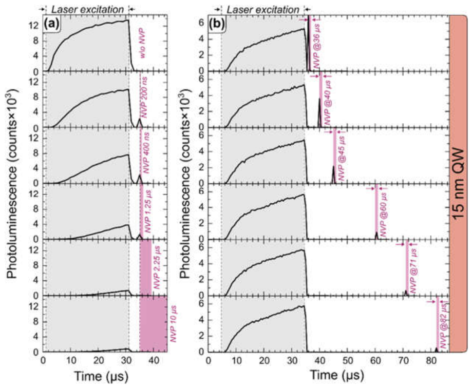
Figure 14.
(a) PL pulses from LED with 25 nm well for different positions of NVP (-10V, 10 s) relative to the laser pulse (given in the inset), black dashed line shows the PL pulse without NVP, (b) integrated PL intensity versus position of NVP with respect to the laser pulse. The dash-dotted line corresponds to the integrated PL intensity without NVP. The excitation was by 30 s pulses of 2 mW, 405 nm laser diode, and the excitation period was fixed at 30 ms. (reprinted with permission from [13]).
Figure 14.
(a) PL pulses from LED with 25 nm well for different positions of NVP (-10V, 10 s) relative to the laser pulse (given in the inset), black dashed line shows the PL pulse without NVP, (b) integrated PL intensity versus position of NVP with respect to the laser pulse. The dash-dotted line corresponds to the integrated PL intensity without NVP. The excitation was by 30 s pulses of 2 mW, 405 nm laser diode, and the excitation period was fixed at 30 ms. (reprinted with permission from [13]).
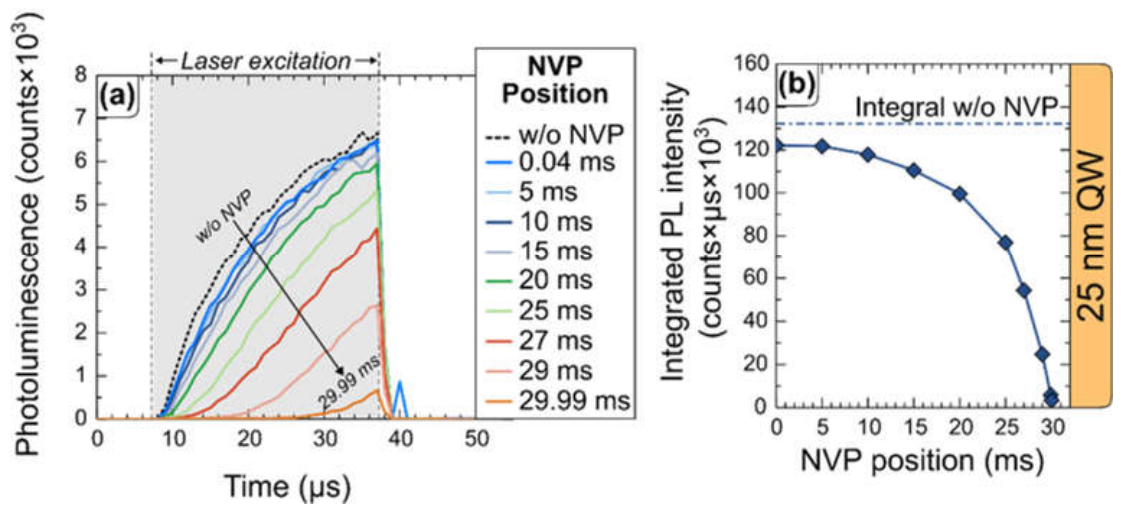
Figure 17.
(a) Schematic structure of the LED, (b) voltage applied to the diode and (c) emission intensity from LED as a function of time (for forward voltage of +2.5V and the period of NVPs equal to 100s), (d) magnified SPL intensity vs time, (e) normalized emission spectrum of SPL at -10V (solid line) and the normalized electroluminescence spectrum of LED at 3.5V (dashed line). (reprinted with permission from [14]).
Figure 17.
(a) Schematic structure of the LED, (b) voltage applied to the diode and (c) emission intensity from LED as a function of time (for forward voltage of +2.5V and the period of NVPs equal to 100s), (d) magnified SPL intensity vs time, (e) normalized emission spectrum of SPL at -10V (solid line) and the normalized electroluminescence spectrum of LED at 3.5V (dashed line). (reprinted with permission from [14]).
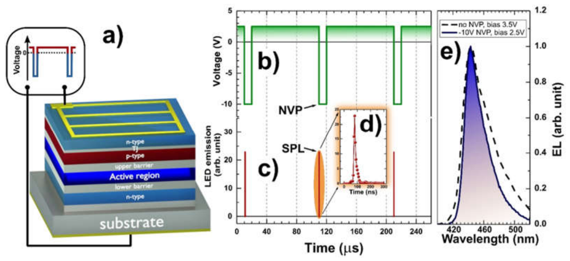
Figure 18.
Integrated intensity of SPLs as a function of separation of 10s NVPs, for different forward voltages applied to the LED and three values of negative NVP voltage: (a) -10V, (b) -5V, (c) -3V. SPLs appear at some threshold separations of NVPs and saturate. They increase for increased forward voltages (currents) between NVPs and for increased negative voltages during NVPs. (reprinted with permission from [14]).
Figure 18.
Integrated intensity of SPLs as a function of separation of 10s NVPs, for different forward voltages applied to the LED and three values of negative NVP voltage: (a) -10V, (b) -5V, (c) -3V. SPLs appear at some threshold separations of NVPs and saturate. They increase for increased forward voltages (currents) between NVPs and for increased negative voltages during NVPs. (reprinted with permission from [14]).
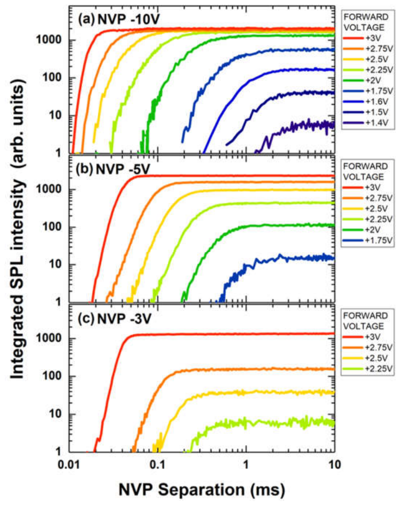
Figure 19.
SPL intensity as a function of NVP separation (charging time) for three values of negative voltage applied during NVP: (a) -10V, (b) -5V, (c) -3V and for increasing duration of NVP (from 100ns up to 1ms). Here the forward voltage applied to LED was 2.5V and only the parameters of NVP (voltage and duration) were varied. When NVP duration is long enough, dark charge is depleted during NVP and SPL intensity vs charging time stabilizes. (reprinted with permission from [14]).
Figure 19.
SPL intensity as a function of NVP separation (charging time) for three values of negative voltage applied during NVP: (a) -10V, (b) -5V, (c) -3V and for increasing duration of NVP (from 100ns up to 1ms). Here the forward voltage applied to LED was 2.5V and only the parameters of NVP (voltage and duration) were varied. When NVP duration is long enough, dark charge is depleted during NVP and SPL intensity vs charging time stabilizes. (reprinted with permission from [14]).
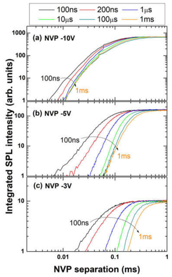
Figure 20.
Band diagrams for LED at four moments (t1, t2, t3, t4) of the periodic experimental procedure (marked in (a)), starting from top left: (b) depleted well at 2.75V, (c) charged well after 1.5ms charging time at 2.75V, (d) charged well just after application of NVP at -10V, (e) discharged well at the end of NVP pulse at -10V. Quasi-Fermi levels are shown with dashed lines for electrons (blue) and for holes (red). Expanded band diagrams in the well region (together with electron and hole charge densities) are shown in the inserts. (reprinted with permission from [14]).
Figure 20.
Band diagrams for LED at four moments (t1, t2, t3, t4) of the periodic experimental procedure (marked in (a)), starting from top left: (b) depleted well at 2.75V, (c) charged well after 1.5ms charging time at 2.75V, (d) charged well just after application of NVP at -10V, (e) discharged well at the end of NVP pulse at -10V. Quasi-Fermi levels are shown with dashed lines for electrons (blue) and for holes (red). Expanded band diagrams in the well region (together with electron and hole charge densities) are shown in the inserts. (reprinted with permission from [14]).
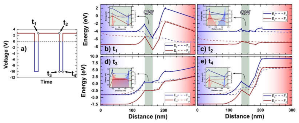
Figure 21.
Concentration of electrons in the quantum well for different dc forward voltages applied to LED (as indicated in the legend). This simulation starts right after NVP at t1 moment. Corresponding current densities (in mA/cm2) are also listed in the legend. (reprinted with permission from [14]).
Figure 21.
Concentration of electrons in the quantum well for different dc forward voltages applied to LED (as indicated in the legend). This simulation starts right after NVP at t1 moment. Corresponding current densities (in mA/cm2) are also listed in the legend. (reprinted with permission from [14]).
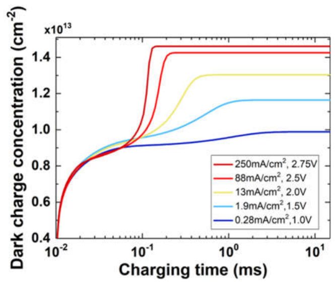
Figure 22.
Simulated intensity of SPLs (generated by 10s, -10V NVPs) as a function of charging time before NVP, for different forward voltages applied to the LED (indicated in the legend, together with corresponding current densities in mA/cm2). (reprinted with permission from [14]).
Figure 22.
Simulated intensity of SPLs (generated by 10s, -10V NVPs) as a function of charging time before NVP, for different forward voltages applied to the LED (indicated in the legend, together with corresponding current densities in mA/cm2). (reprinted with permission from [14]).
Disclaimer/Publisher’s Note: The statements, opinions and data contained in all publications are solely those of the individual author(s) and contributor(s) and not of MDPI and/or the editor(s). MDPI and/or the editor(s) disclaim responsibility for any injury to people or property resulting from any ideas, methods, instructions or products referred to in the content. |
© 2026 by the authors. Licensee MDPI, Basel, Switzerland. This article is an open access article distributed under the terms and conditions of the Creative Commons Attribution (CC BY) license (http://creativecommons.org/licenses/by/4.0/).
Copyright: This open access article is published under a Creative Commons CC BY 4.0 license, which permit the free download, distribution, and reuse, provided that the author and preprint are cited in any reuse.