

Submitted:
18 June 2026
Posted:
22 June 2026
You are already at the latest version
Abstract
The present research work compares graphene/PMMA-based nanocomposites prepared with various modified graphene nanoparticles to develop polymer-based nanocomposites with enhanced electromagnetic interference (EMI) shielding efficiency. A metal-decorated graphene (G/Ag) nanostructure was compared with an irradiated hybrid carbon nanostructure comprising graphene and multi-walled carbon nanotubes (G/CNTs). Three representative composites with varying filler loadings (15–20 wt%), thicknesses (0.208–0.48 mm), and an e-beam irradiation dose of 50 kGy were systematically characterized using SEM, FTIR, TGA/DSC, and vector network analyzer (VNA) measurements in the S-band (2.65–3.90 GHz). The effects of these different modifications (metal decoration or e-beam irradiation) on conductive network construction, interface engineering, and the resulting porous or layered structures on EMI shielding performance are discussed. All tested composites exhibited a strongly absorption-dominant behavior. Better EMI shielding effectiveness (SE) results were obtained for the irradiated PMMA/АМ1 (50 kGy) sample (d = 0.48 mm) and the PMMA/AH50 sample (d = 0.28 mm), reaching up to 11–13 dB compared to the metal-decorated PMMA/G/Ag nanocomposite. The obtained results confirmed that by increasing the sample thickness and the G/CNT hybrid content, the EMI shielding performance was significantly enhanced due to a greater absorption volume and denser conductive networks. This demonstrates the potential of irradiated graphene/CNT–PMMA nanocomposites as lightweight EMI shielding materials for various electronic and biomedical devices.
Keywords:
electrical properties
; graphene
; G-MWCNT hybrid
; nanocomposites
; PMMA
; EMI shielding
Introduction
In the last decade, due to the rapid development of telecommunications and the increased application of wireless communications, the human population has been increasingly exposed to electromagnetic radiation from various electronic devices incorporated into smart buildings. Because this electromagnetic pollution causes serious operational and health-related problems, electromagnetic interference (EMI) shielding has attracted great interest. Practically, EMI shielding is achieved by minimizing the signal transfer through a system via surface reflections and/or the absorption of the radiated power. Different metal-based EMI shielding materials have been developed and are widely available on the market. In recent years, intensive research has focused on the design and development of new polymer-based composite materials filled with various conductive graphene nanostructures, aimed at producing more efficient EMI shielding materials and protection [1,2]. Generally, polymer nanocomposites filled with graphene, multi-walled carbon nanotubes (MWCNTs), or their hybrids are attractive alternatives due to their unique combination of electrical, thermal, dielectric, magnetic, and mechanical properties. The main challenges are related to the application of specific graphene nanostructures with higher electrical conductivity, as well as the optimization of processing techniques to obtain a uniform dispersion within the polymer matrix. By combining two-dimensional (2D) graphene sheets with one-dimensional (1D) MWCNTs, the 1D tubes can physically bridge adjacent 2D graphene layers, constructing a more robust three-dimensional interconnected conductive network that effectively lowers the percolation threshold. Therefore, the main research goals focus on the design and development of thin, lightweight, highly flexible, next-generation smart materials capable of absorbing strong electromagnetic (EM) radiation over a wide frequency range [3,4].
Since its discovery in 2004, graphene has become one of the most attractive carbon-based nanostructures. Graphene is the foundational structural unit of all graphitic materials, giving it enormous application potential in various sectors, from the electrical industry, nanoelectronics, and environmental nanosensors to medicine and diagnostics [1,2]. Due to the sp2-hybridized carbon atoms in the monolayer graphene lattice, it has a very low mass density compared to conventional fillers and possesses high electrical and thermal conductivity. Besides its very efficient conductivity, graphene exhibits superior mechanical behavior and is estimated to be significantly stronger than steel. Due to this superior electrical conductivity (higher than 107 S m-1), excellent mechanical properties (exceptional mechanical strength and flexibility), and high specific surface area (resulting in a light and durable structure), graphene has been intensively tested as an ideal nanofiller in polymer nanocomposites for efficient electromagnetic shielding applications. Graphene can very effectively dissipate absorbed electromagnetic radiation, reducing overheating risks and ensuring device reliability [4,5]. However, some critical factors that affect the EMI shielding efficiency in graphene-based polymer nanocomposites include the filler loading, uniform graphene dispersion, and the resulting morphology of the graphene and modified graphene nanostructures inside the polymer matrices [6,7].
In order to improve the absorption performance of the EMI shielding effectiveness (SE) of graphene/polymer nanocomposites, some of the latest research trends are directed towards the modification of graphene by the incorporation of dielectric and/or magnetic nanoparticles. The incorporation of dielectric nanoparticles into graphene nanostructures has become one of the most efficient strategies to extend loss mechanisms beyond conduction alone. Dielectric nanoparticles, including titanium dioxide (TiO2), barium titanate (BaTiO3), nickel oxide (NiO), aluminum oxide (Al2O3), and silicon carbide (SiC), can introduce interfacial polarization, dipole relaxation, and space-charge accumulation [8,9]. As a result of the formation of heterojunctions between the graphene layers and dielectric fillers, Maxwell–Wagner–Sillars (MWS) polarization is induced [10], thereby enhancing dielectric loss within the microwave frequency range. Furthermore, these dielectric fillers disrupt the continuity of the graphene conductive network, resulting in increased internal scattering and improved impedance matching—critical factors for maximizing absorption while minimizing specular reflection. Similar effects have also been achieved through the irradiation treatment of graphene nanostructures [11,12]. Specifically, electron-beam irradiation can induce controlled structural defects, cross-linking, and localized charge centers within the carbon nanostructures, which alter their complex permittivity and create additional sites for polarization loss. For instance, Yuchang et al. worked on tailoring the EMI shielding properties of graphene nanosheets incorporated with BaTiO3 ceramics [13]. Their results showed that both the real and imaginary components of the complex permittivity increased with higher graphene nanosheet (GN) content. The results regarding EMI shielding effectiveness indicated that the absorption mechanism was the primary contributor to the overall EMI SE. The total EMI SE surpassed 40 dB in the X-band at a thickness of 1.5 mm, suggesting that GN/BaTiO3 ceramics are excellent candidates for highly efficient EMI shielding materials throughout the X-band [13]. Bhaskaran et al. analyzed the EMI shielding effectiveness of epoxy nanocomposites with graphene nanoplatelets (GNPs) and Fe3O4 nanoparticles, referred to as Fe3O4/GNP hybrids, in the frequency range of 8–12.4 GHz. A series of epoxy nanocomposites with different ratios of Fe3O4/GNP, GNPs, and/or Fe3O4 nanoparticles was developed and assessed for their EMI SE. Overall, the incorporation of Fe3O4/GNP hybrids resulted in enhanced EMI shielding performance compared to samples containing only GNPs or Fe3O4 in equivalent amounts [14]. Additionally, Q. Lu investigated the application of e-beam and neutron-irradiation effects on the EMI SE of nanocomposite materials [15]. They studied MWCNT-based composites irradiated to fluence levels of 1016 electrons/cm2 with 500 keV electrons. An increase in EMI SE and conductivity was observed following electron irradiation in two of the tested epoxy-based systems.
However, a direct comparative assessment of how chemical metal decoration versus high-energy physical e-beam irradiation modifies the local interface and porous topology within a PMMA matrix for S-band attenuation remains largely unexplored. This paper reports a comparative study of the EMI SE of PMMA-based nanocomposite materials reinforced with two different treated graphene nanostructures: metal-modified graphene (G/Ag) and an e-beam-irradiated graphene/MWCNT hybrid, designated as AM1 and AH50, respectively.
Experiment
In this work, polymer nanocomposites were prepared using poly(methyl methacrylate) (PMMA) as the polymer matrix and various modified carbon-based nanostructures comprising graphene (G) and a hybrid of graphene and multi-walled carbon nanotubes (graphene/MWCNTs) (commercially supplied from China) as fillers. The graphene nanoplatelets were chemically modified with silver nanoparticles to form a G/Ag hybrid. The hybrid graphene/MWCNT nanostructures (designated as AH50 and AM1) were irradiated with an electron beam (e-beam) at a dose of 50 kGy at the Institute of Applied Radiation Chemistry, Lodz University of Technology, Poland. The corresponding polymer nanocomposite films were fabricated via the solvent casting method.
Characterization of the modified graphene nanostructures and the resulting PMMA composites was performed using several analytical methods. The morphologies of the pristine and irradiated carbon hybrid nanostructures, as well as the composite films, were observed by scanning electron microscopy (SEM) (JEOL, model JSM-1200). Transmission electron microscopy (TEM) observation of the prepared samples was performed using a FEI Tecnai G2 Spirit TWIN transmission electron microscope equipped with a LaB6 cathode.
Thermogravimetric analysis (TGA) and differential scanning calorimetry (DSC) measurements were performed on composite samples (approx. 20 mg) using a simultaneous TGA/DSC thermal analyzer (Themis One+, SETARAM–Keep Technologies, France) under a nitrogen atmosphere, at a heating rate of 10 °C min-1 over a temperature range of 30–800 °C. Fourier-transform infrared spectroscopy with attenuated total reflection (FTIR-ATR) spectra were recorded in the 3500–400 cm-1 wavenumber range using a Varian 660 FT-IR spectrometer (Agilent Technologies, USA). Electrical conductivity was determined by the four-probe method using a Jandel RM3000 instrument.
The electromagnetic interference shielding effectiveness (EMI SE) measurements were performed using a Keysight P9370A vector network analyzer (VNA). The dimensions of the test samples matched the internal dimensions of the standard WR-90 waveguide adapters used for electromagnetic shielding measurements. The scattering and transmission coefficients were evaluated in the frequency ranges of 1.70–2.60 GHz and 2.60–3.95 GHz. The WR-90 waveguide adapters were connected to ports 1 and 2 of the VNA using precision RF coaxial cables. The samples were placed securely between the two waveguide adapters, and the values of the S21 scattering coefficients were collected. All measurements were performed at room temperature.
Results and Discussion
Characterization of Modified Graphene
Different modification treatments of the pristine graphene-based nanostructures resulted in distinct morphological forms of the graphene microstructure. The observed microstructural changes are presented in Figure 1. As seen in Figure 1a, the pristine graphene (G0) exhibits a highly aggregated, layered, and wrinkled sheet morphology typical of unmodified nanoplatelets. co-network.
Silver (Ag) nanoparticles are successfully decorated mainly on the surface of the graphene nanoplatelets (Figure 1b), where bright, spherical nanoparticles are uniformly anchored across the flakes, preventing restacking and creating additional interfacial heterojunctions. In the non-irradiated hybrid (Figure 1c), the 1D multi-walled carbon nanotubes are intertwined and distributed among the 2D graphene sheets, forming an initial entangled. Due to the e-beam irradiation of the hybrid graphene/MWCNT nanostructure, additional exfoliation of the graphene sheets was induced, accompanied by structural defects (Figure 1d). The high-energy electron beam induces radiolysis and structural displacement, which lead to a more porous, loosely packed network with visible uncoiling and fragmentation of the tubes. This expanded, highly defective porous topology is highly beneficial for EMI shielding, as it enhances multi-internal reflections and impedance matching within the PMMA matrix.
A comparison of the TGA and DSC thermograms of the metal-modified graphene and e-beam-irradiated graphene/MWCNTs is shown in Figure 2 and Figure 3, respectively. The TGA thermograms of the modified graphene nanostructures showed three temperature zones with distinctive mass loss steps: the first region (~100 °C) usually associated with the loss of adsorbed moisture, the second region (100–360 °C) associated with the breakdown of thermally labile oxygen-containing groups, and the third region (360–700 °C) associated with the decomposition of the carbon lattice. Evidently, the applied modifications induced significant changes in the graphene carbon lattice, leading to a decrease in thermal stability. The decoration of graphene with Ag (30 wt.%) induces structural defects within the graphene sheets, which lowers the onset decomposition temperature. An analogous trend, though significantly more pronounced, was observed for the e-beam-irradiated graphene/MWCNT sample (AM1). Specifically, the TGA curve of the AM1 sample (Figure 2) reveals a multi-step weight loss profile starting below 150 °C, which corresponds to the thermal desorption of radiation-induced functional groups and the accelerated decomposition of highly defective carbon networks. Correspondingly, the DSC thermograms (Figure 3) exhibit distinct exothermic and endothermic transitions between 300 °C and 450 °C, confirming altered crystalline phases and phase transition kinetics due to decoration and irradiation.
Characterization of G/PMMA Nanocomposites
The typical microstructure of the obtained PMMA-based nanocomposites is shown in Figure 4. In all prepared nanocomposite samples, microstructural inhomogeneity was observed due to the presence of residual micropores. These pores were induced by solvent evaporation during the solvent casting fabrication process.
The TGA thermograms, presented in Figure 5, show that the incorporation of modified carbon nanostructures (specifically graphene and graphene/MWCNT hybrids) into the PMMA matrix improved the overall thermal stability of the resulting nanocomposites. This enhancement is attributed to the uniform dispersion of the carbon-based fillers within the polymer macromolecular network, which acts as a physical barrier to volatile degradation products. However, the highest thermal stability was registered for the PMMA nanocomposite reinforced with the irradiated hybrid nanostructure sample, PMMA/AH50 (50 kGy).
The DSC thermograms are shown in Figure 6. These curves complement the TGA data, confirming the influence of the variously modified graphene and graphene/MWCNT hybrid nanostructures on the thermal transitions of the matrix. Specifically, the characteristic degradation peak temperatures of the PMMA matrix were shifted to higher temperatures in the nanocomposites, indicating a higher activation energy for thermal decomposition due to restricted polymer chain mobility near the nanofiller interfaces.
The FTIR spectra of modified graphene/PMMA nanocomposites, scanned in the range from 500 to 3500 cm-1, are shown in Figure 7. Interpretation of the FTIR spectra in polymer nanocomposite systems can be challenging because the characteristic vibrational bands of the polymer matrix and the graphene-based nanostructures often overlap, potentially leading to broad or merged signals. From Figure 7, it is evident that no new absorption peaks appear upon the incorporation of the variously treated graphene fillers into the PMMA matrix. This suggests an absence of new covalent bonding between the PMMA and the graphene nanostructures, indicating that the metal-functionalized and irradiated carbon nanostructures were predominantly physically dispersed or intercalated within the polymer matrix.
All spectra exhibit the characteristic C–H stretching band of the methylene groups at 2996 cm-1 and 2947 cm-1, C–H bending vibration peaks around 1447 cm-1 and 1388 cm-1, and C–O–C stretching modes of the PMMA ester groups showing multiple peaks in the 1300 and 1000 cm-1 region. Notably, the C=O stretching band exhibits a slight drop in intensity and a minor shift, suggesting a physical interaction between the ester carbonyl groups of PMMA and the surface functional groups or π -electron networks of the graphene sheets. This interface adhesion, governed by physical adsorption or weak van der Waals forces, induces alterations in the local chemical environment, leading to the observed intensity variations and shifts in both the C–H and C–O–C structural zones. These changes confirm that the conformation of the PMMA matrix is influenced by the incorporation of the graphene-based nanostructures, which is favorable for enhancing subsequent mechanical and electrical characteristics.
Theoretically, the incorporation of graphene-based nanostructures leads to the formation of conductive pathways within the polymer matrix, thereby significantly improving the electrical conductivity (σ) of the fabricated nanocomposite films. Graphene's high aspect ratio and extensive surface area facilitate the establishment of a continuous conductive network within the PMMA matrix, which enhances the dielectric properties through improved polarization and charge transfer mechanisms. This interfacial interaction promotes the creation of numerous micro-capacitors by trapping migrating charge carriers at the heterogeneous interfaces between the graphene phases and the insulating PMMA matrix—a phenomenon known as interfacial (or Maxwell–Wagner–Sillars) polarization.
The measured data for the electrical conductivity of the obtained composites are given in Table 1. As expected, neat PMMA exhibits an insulating behavior with a conductivity of 2.3 × 10⁻¹³ S/m. Upon the introduction of the modified carbon nanostructures, the electrical conductivity increases sharply by several orders of magnitude, indicating that the filler loading exceeds the electrical percolation threshold. The highest conductivity value is observed for the PMMA/AM1 sample (3.41 × 10^-1 S/m), which can be attributed to the efficient e-beam-induced network restructuring and dense local connectivity of the graphene/MWCNT hybrid.
The measured electromagnetic interference shielding effectiveness (EMI SE) of the fabricated PMMA-based nanocomposite films is presented in Figure 8 and Figure 9. The obtained results demonstrate that both types of modified graphene-based nanostructures (the silver-decorated G/Ag and the irradiated graphene/MWCNT hybrid) confer an absorption-dominant shielding mechanism to the composites. These nanocomposites exhibit shielding performance suitable for moderate-attenuation electronic applications. Significantly better results were obtained for the irradiated PMMA/AM1 sample (d = 0.48 mm) and the PMMA/AH50 sample (d = 0.28 mm), which exhibited the highest shielding performance, reaching up to 11–13 dB across the evaluated S-band frequency range. In contrast, the pure PMMA reference provided minimal attenuation (< 1 dB), confirming the critical role of the carbonaceous network from the G-CNT filler. The enhanced performance of the irradiated hybrid systems, particularly at greater sample thicknesses, underscores the synergy between network density and volume interaction. These results confirm that increasing the sample thickness and graphene/MWCNT hybrid content directly enhances EMI shielding efficiency by expanding the effective absorption volume and establishing denser conductive networks. Furthermore, the positive effect of e-beam irradiation is attributed to improved filler dispersion, the generation of localized structural defects that promote polarization losses, and enhanced interfacial bonding with the surrounding PMMA matrix.
The PMMA/G/Ag nanocomposite sample exhibited relatively poor EMI shielding efficiency. Namely, at 2 GHz, the difference in the amplitude of the transmission coefficient (S21) was around 5 dB, which corresponds to approximately 31.6% of the radiofrequency (RF) power being transmitted through the sample (or an attenuation leaving only ~15% of the initial signal power). Consistent with the findings of Stefanović A., et al. [16], and in contrast to the PMMA/G/Ag composites, both composites reinforced with irradiated graphene/MWCNT nanostructures showed enhanced EMI shielding capabilities. The highest value was achieved for the PMMA/graphene/MWCNT composite with a thickness of 0.48 mm.
Conclusions
This study successfully evaluated and compared the effects of different nanostructure modifications, specifically chemical silver-decoration (G/Ag) and high-energy electron-beam (e-beam) irradiation, on conductive network construction, interface engineering, and the resulting network morphology on the EMI shielding performance of PMMA-based nanocomposites. The structural characterizations confirmed that these modifications induced significant microstructural alterations in the carbon fillers. These changes directly influenced the macromolecular network of the host PMMA matrix, culminating in enhanced thermal stability, improved electrical conductivity, and efficient charge transfer due to intensified Maxwell–Wagner–Sillars interfacial polarization. All tested nanocomposite films exhibited a strongly absorption-dominant shielding behavior. Superior EMI SE results were obtained for the irradiated hybrid samples, namely the PMMA/AM1 (50 kGy) sample (d = 0.48 mm) and the PMMA/AH50 sample (d = 0.28 mm), which achieved attenuation levels of 11–13 dB, significantly outperforming the silver-decorated PMMA/G/Ag nanocomposites. The obtained results confirmed that by increasing both the sample thickness and the graphene/MWCNT hybrid content, the EMI shielding effectiveness was enhanced. This improvement is attributed to an expanded absorption volume and the formation of denser, more interconnected conductive networks, demonstrating the high potential of irradiated graphene/MWCNT–PMMA nanocomposites as lightweight, absorption-driven EMI shielding materials for electronic devices.
Funding
The Ministry of Science and Education of the Republic of North Macedonia has financially supported this investigation in the frame of the project Graphene-polymer based nanocomposites for EMI shielding in smart buildings (2025-2026, Grant No. 05-923).
Data Availability Statement
The original contributions presented in this study are included in the article. Further inquiries can be directed to the corresponding author.
Acknowledgments
We acknowledge the use of Grammarly software for grammar checking and language enhancement to improve the clarity and readability of this manuscript.
Conflicts of Interest
The authors declare no conflicts of interest.
References
- Bakr, A. M.; Darwish, A.; Azab, A. A.; Elzwawy, A. Polym. Bull. 2025, 82, 5771–5795. [CrossRef]
- Grozdanov, A.; Paunovic, P.; Dimitrievska, I.; Proseva, M.; Gorgieva, A.; Castaldo, R.; Gentile, G. J. of Nanotechnology 2026, 8823129. [CrossRef]
- Ruiqi, N.; Jinying, L.; Guibin, W.; Shuling, Z. RSC Adv. 2018, 8, 3296.
- Kumar, R. B.; Gopu, J.; Bhaskaran, K.; Verma, A.; Chavali, M.; Etika, K. C. Nanoscale Adv. 2024, 6, 5773. [CrossRef]
- Sebastian, A.; Raghavan, A. International Res. J. Adv. Eng. Hub (IRJAEH) 2024, 2(5), 1334–1340. [CrossRef]
- Kausar, A.; Ahmad, I.; Zhao, T.; Aldaghri, O.; Lam, T. D. J. Compos. Sci. 2023, 7, 384. [CrossRef]
- Jovanović, S.; Huskić, M.; Kepić, D.; Yasir, M.; Haddadi, K. Graphene 2D Mater. 2023, 8, 59–80. [CrossRef]
- Kumar, P.; Narayan Maiti, U.; Sikdar, A.; Kumar Dasb, T.; Kumar, A.; Sudarsan, V. Polym. Rev. 2019, 59, 687–738. [CrossRef]
- Bagotia, N.; Choudhary, V.; Sharma, D. K. Polym. Adv. Technol. 2018, 29, 1547–1567. [CrossRef]
- Markovic, Z.; Budimir, M.; Kepic, D.; Holclajtner-Antunovic, I.; Marinovic-Cincovic, M.; Dramicanin, M.; Spasojevic, V.; Peruško, D.; Špitalský, Z.; Micušik, M. RSC Adv. 2016, 6, 39275–39283. [CrossRef]
- Paunović, P.; Grozdanov, A.; Makreski, P.; Gentile, G. J. Eng. Mater. Technol. 2020, 142, 0410031–0410036.
- Zagho, M. M.; Al Maadeed, M. A. A.; Majeed, K. Emergent mater. 2020, 3, 675–683. [CrossRef]
- Yuchang, Q.; Qinlong, W.; Fa, L.; Wancheng, Z.; Dongmei, Z. J. Mater. Chem. C 2016, 4, 371–375. [CrossRef]
- Bhaskaran, K.; Bheema, R. K.; Etika, K.C. Synth. Met. 2020, 265, 116374. [CrossRef]
- Lu, Q. PhD Thesis, Published. Air Force Institute of Technology, Nigeria Air Force University, Nigeria, 22 March 2012.
- Stefanovic, A.; Kepic, D.; Momcilovic, M.; Haddadi, K.; Sebbache, M.; Mead, J.L.; Huskic, M.; Todorovic Markovic, B.; Jovanovic, S. Nanomaterials 2024, 14, 912. [CrossRef] [PubMed]
Figure 1.
SEM micrographs showing the different morphological forms of the graphene-based nanostructures: (a) pristine graphene (G0); (b) silver-decorated graphene (G/Ag); (c) pristine graphene/multi-walled carbon nanotube hybrid (G/MWCNT); and (d) e-beam i-radiated hybrid nanostructure at 50 kGy (AH (G/MWCNT 50 kGy)).
Figure 1.
SEM micrographs showing the different morphological forms of the graphene-based nanostructures: (a) pristine graphene (G0); (b) silver-decorated graphene (G/Ag); (c) pristine graphene/multi-walled carbon nanotube hybrid (G/MWCNT); and (d) e-beam i-radiated hybrid nanostructure at 50 kGy (AH (G/MWCNT 50 kGy)).
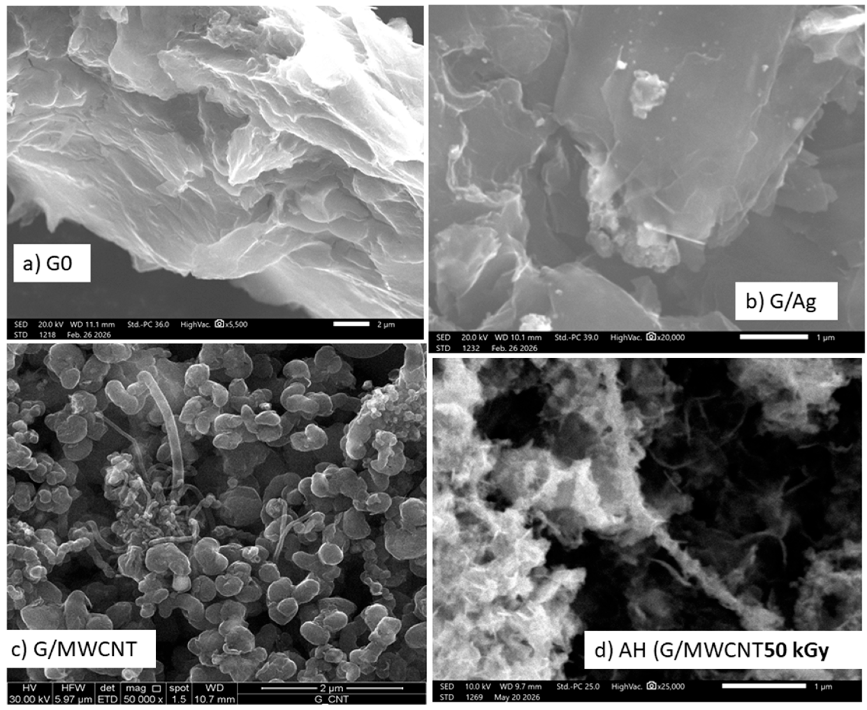
Figure 2.
TGA thermograms of pristine graphene (G), silver-decorated graphene (G+Ag(30%), and e-beam-irradiated hybrid carbon nanostructures (AM1(20%G+CNTs)).
Figure 2.
TGA thermograms of pristine graphene (G), silver-decorated graphene (G+Ag(30%), and e-beam-irradiated hybrid carbon nanostructures (AM1(20%G+CNTs)).
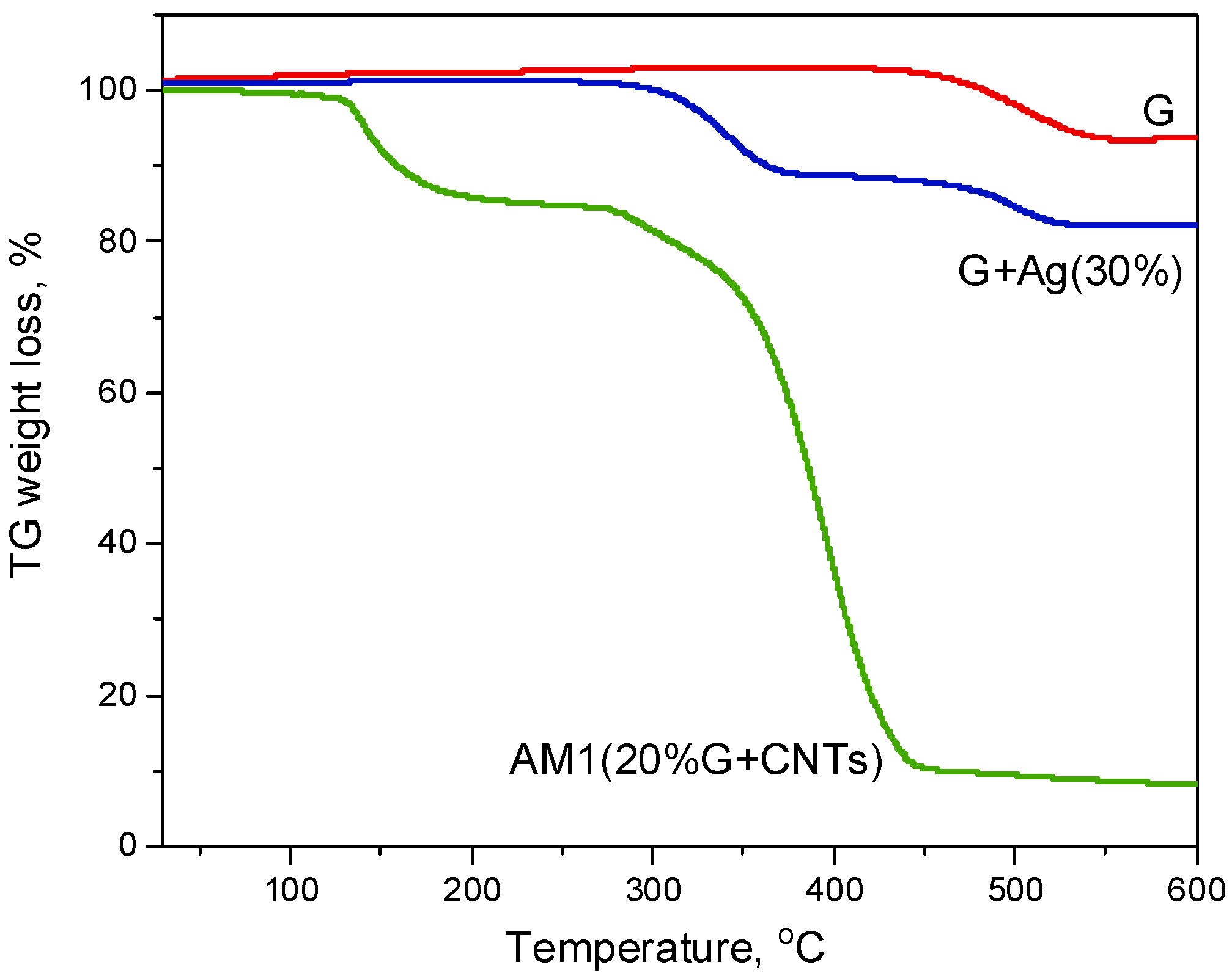
Figure 3.
DSC thermograms of pristine graphene (G), silver-decorated graphene (G+Ag(30%)), and e-beam irradiated hybrid carbon nanostructures (AM1(20%G+CNTs)).
Figure 3.
DSC thermograms of pristine graphene (G), silver-decorated graphene (G+Ag(30%)), and e-beam irradiated hybrid carbon nanostructures (AM1(20%G+CNTs)).
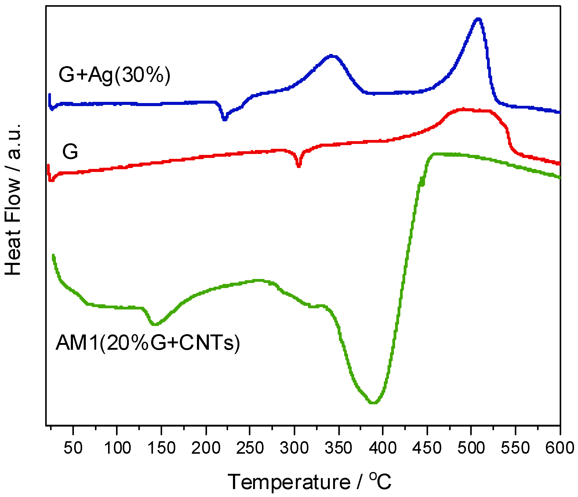
Figure 4.
SEM images of the PMMA-based nanocomposites with various treated graphene.
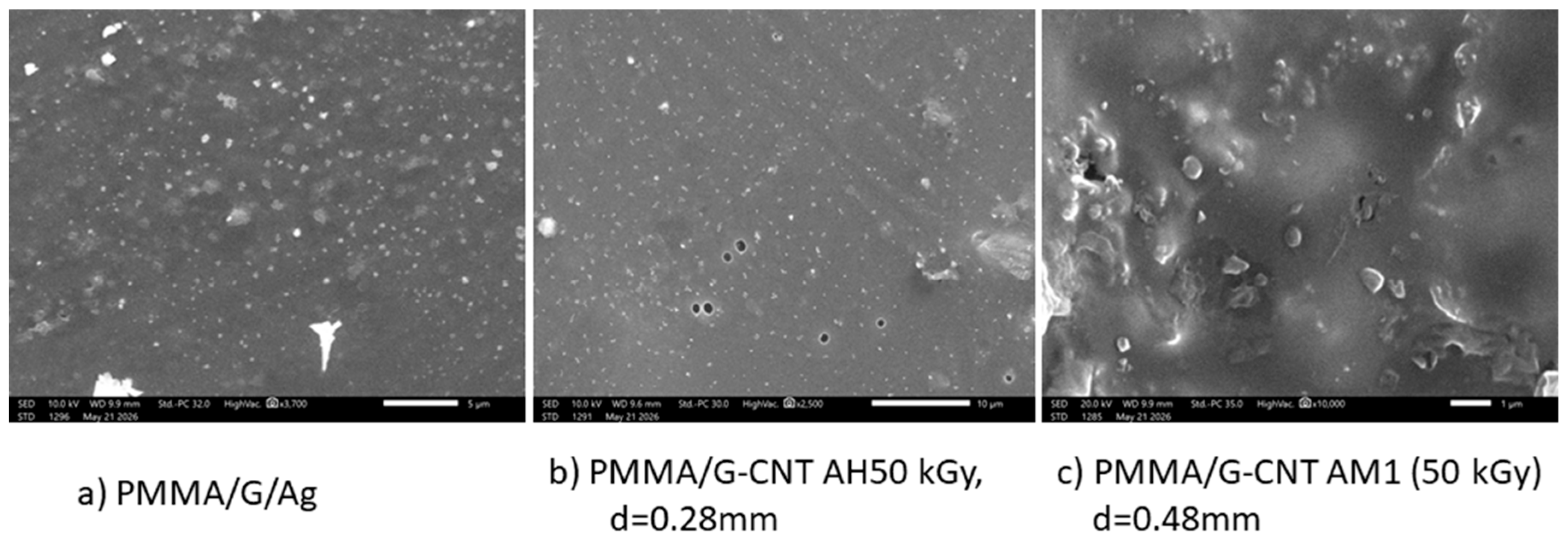
Figure 5.
TGA thermograms of neat PMMA and PMMA-based nanocomposites.
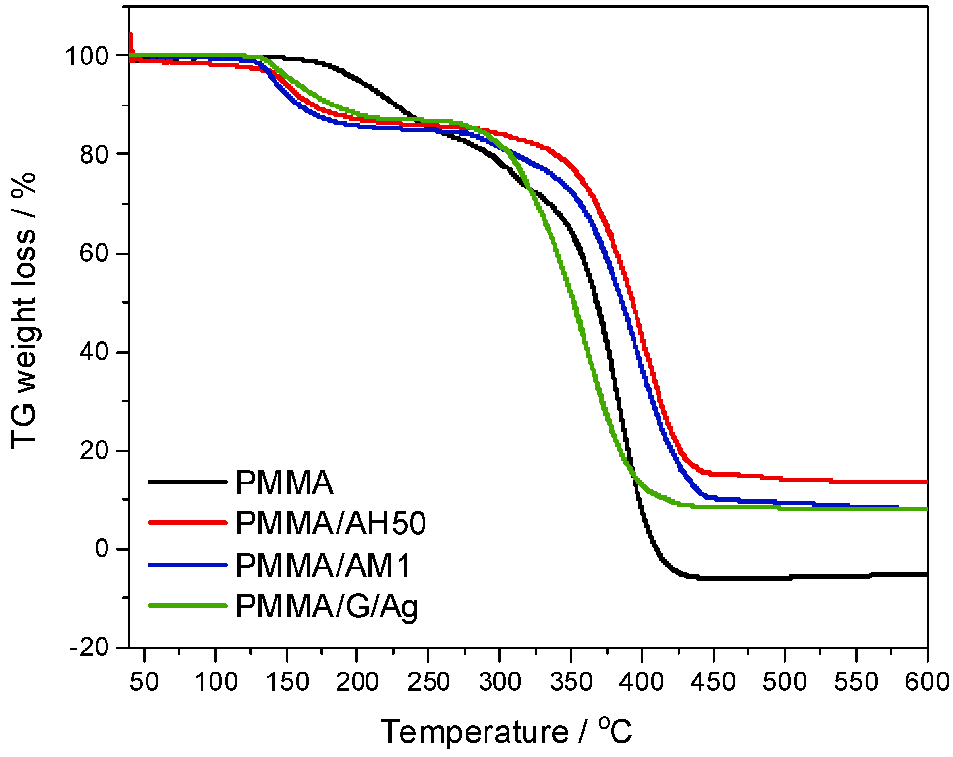
Figure 6.
DSC thermograms of neat PMMA and PMMA-based nanocomposites.
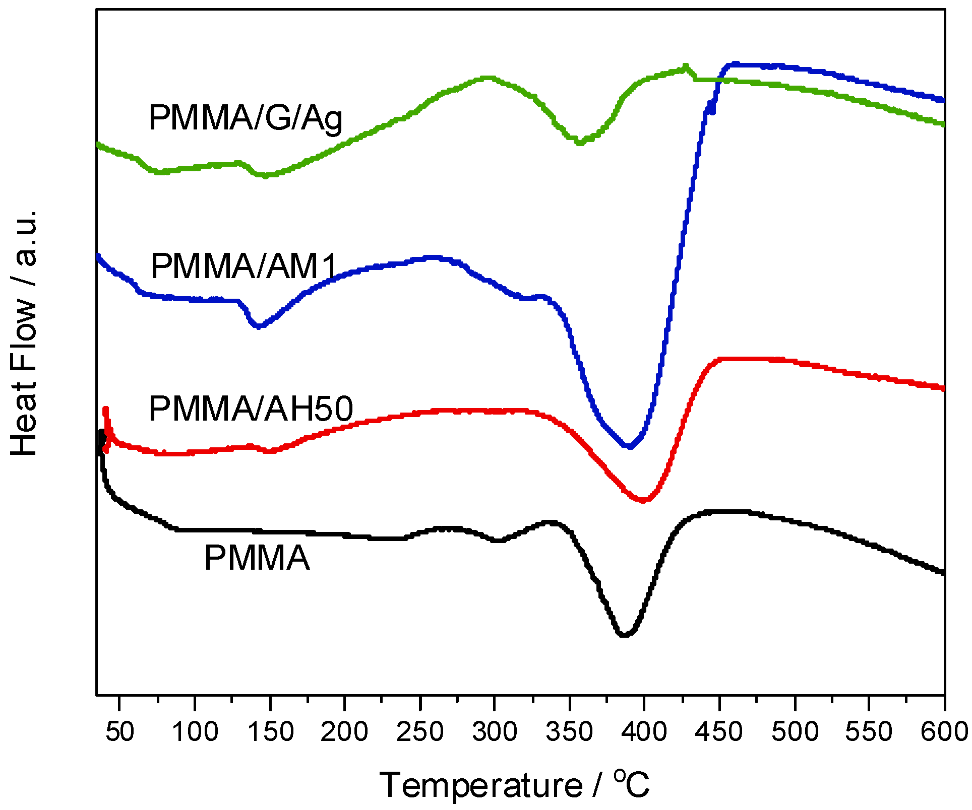
Figure 7.
FTIR spectra of neat PMMA and modified graphene/PMMA nanocomposite films.
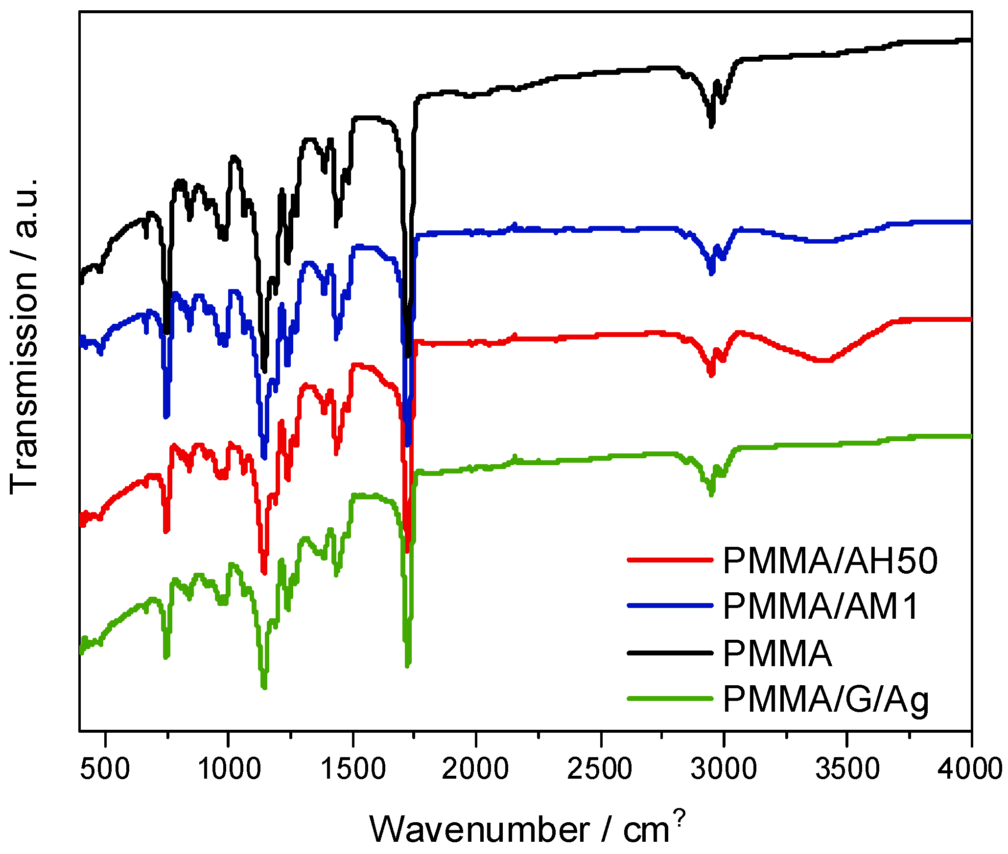
Figure 8.
Total EMI shielding effectiveness (SET) as a function of frequency in the S-band for neat PMMA, PMMA/G/Ag, and PMMA/G-CNT composites.
Figure 8.
Total EMI shielding effectiveness (SET) as a function of frequency in the S-band for neat PMMA, PMMA/G/Ag, and PMMA/G-CNT composites.
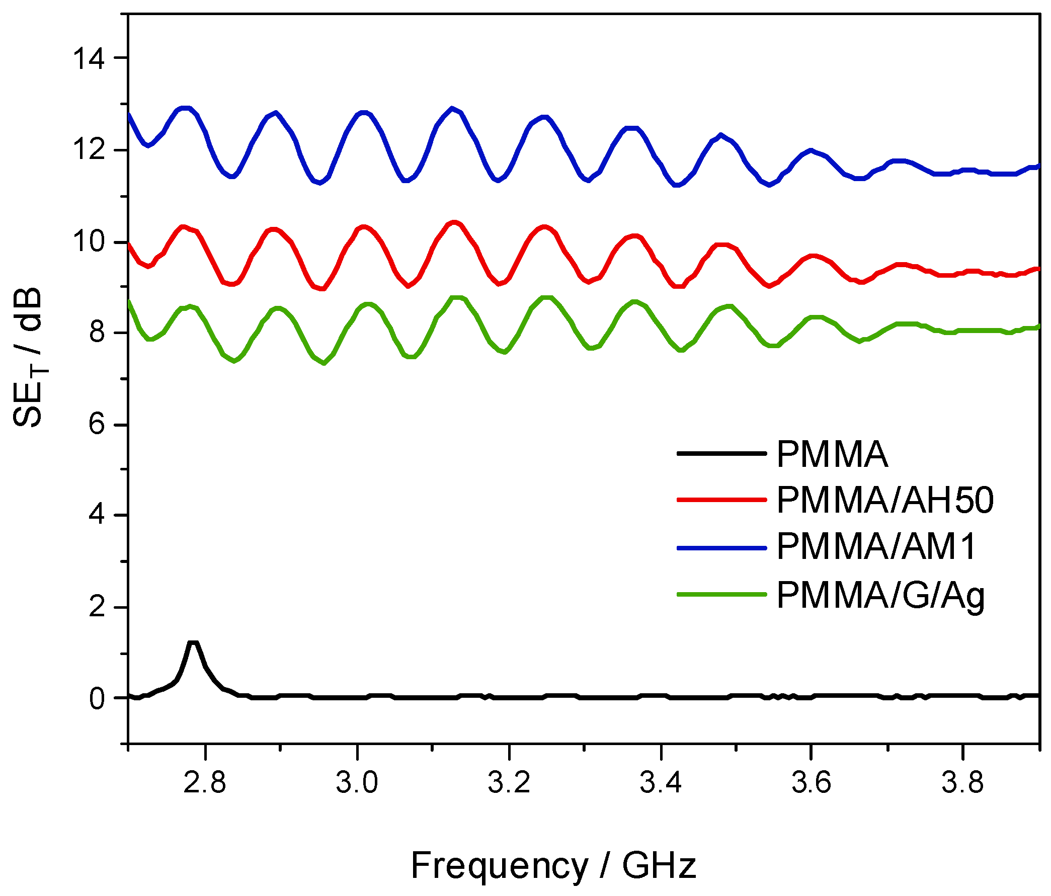
Figure 9.
EMI SE scattering parameters as a function of frequency: (a) S11 scattering coefficient in dB, (b) S21 scattering coefficient in dB, (c) S12 scattering coefficient in dB, (d) S22 scattering coefficient in dB for the studied materials.
Figure 9.
EMI SE scattering parameters as a function of frequency: (a) S11 scattering coefficient in dB, (b) S21 scattering coefficient in dB, (c) S12 scattering coefficient in dB, (d) S22 scattering coefficient in dB for the studied materials.
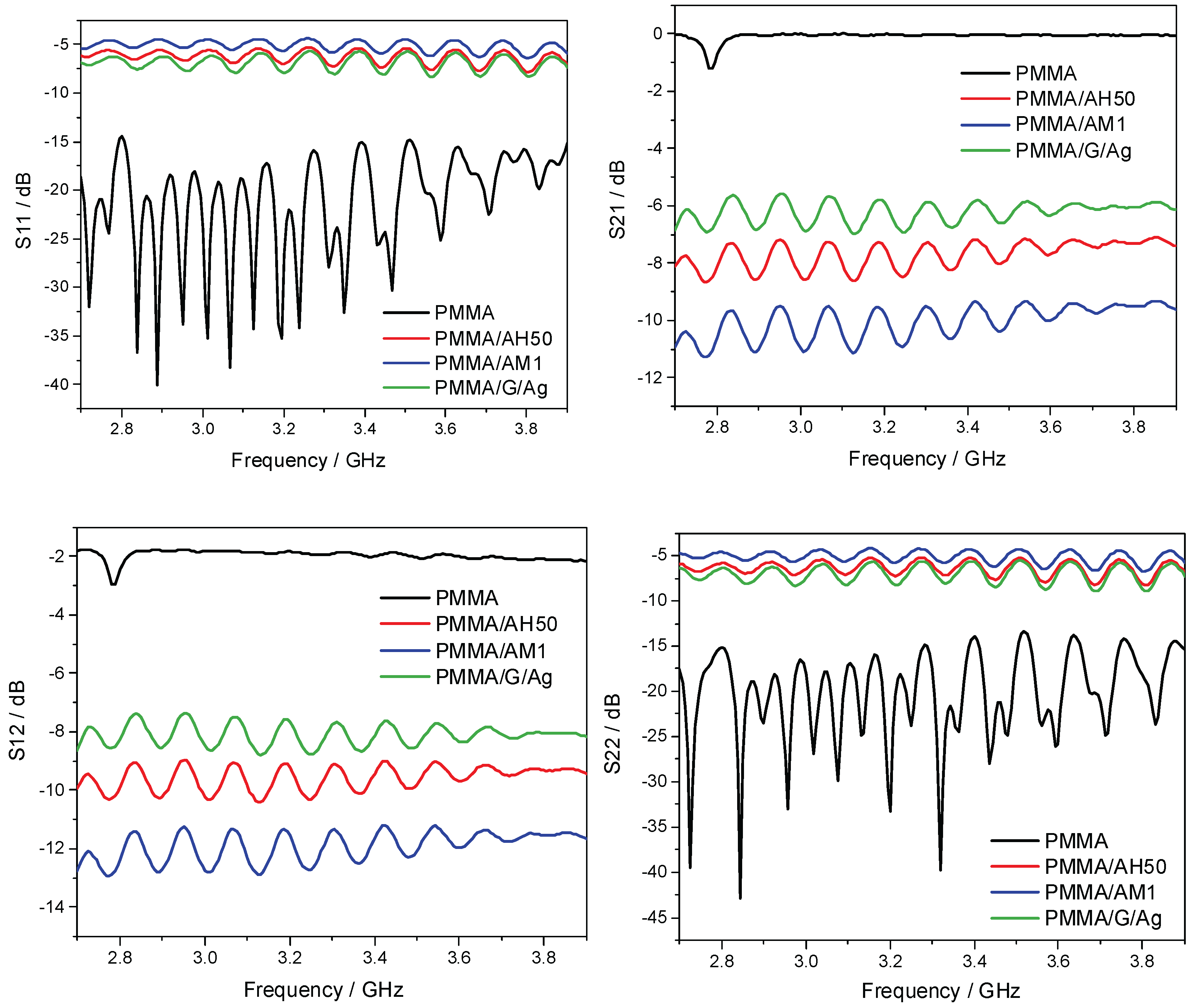

Table 1.
Electrical conductivity (σ) and thickness (d) of the neat PMMA and prepared nanocomposites.
Table 1.
Electrical conductivity (σ) and thickness (d) of the neat PMMA and prepared nanocomposites.
| Sample | d [mm] | σ [S/m] |
| PMMA | 0.19 | 2.3 × 10⁻¹³ |
| PMMA/G/Ag | 0.30 | 9.27 × 10⁻⁵ |
| PMMA/AH50 | 0.28 | 4.18 × 10⁻² |
| PMMA/AM1 | 0.48 | 3.41 × 10⁻¹ |
Disclaimer/Publisher’s Note: The statements, opinions and data contained in all publications are solely those of the individual author(s) and contributor(s) and not of MDPI and/or the editor(s). MDPI and/or the editor(s) disclaim responsibility for any injury to people or property resulting from any ideas, methods, instructions or products referred to in the content. |
© 2026 by the authors. Licensee MDPI, Basel, Switzerland. This article is an open access article distributed under the terms and conditions of the Creative Commons Attribution (CC BY) license (http://creativecommons.org/licenses/by/4.0/).
Copyright: This open access article is published under a Creative Commons CC BY 4.0 license, which permit the free download, distribution, and reuse, provided that the author and preprint are cited in any reuse.


