

Submitted:
14 June 2026
Posted:
15 June 2026
You are already at the latest version
Abstract
Aerosol-assisted chemical vapor deposition (AACVD) was used to prepare thin film of heterojunction WO3/MnO2 onto FTO glass substrate. The WO₃/MnO₂ heterojunction thin film exhibited a monoclinic WO₃ structure characterized by a nanorod-like shape and substantial interfacial bonding. The detected surface area of WO3/MnO2 thin film is 33.14 μm2, while the values of Ra and Rq are 24.8 nm and 31.3 nm, respectively, which are higher than pure MnO2 while lower than pure WO3 thin films. The UV-Vis spectra demonstrated extensive absorption in the visible to near-infrared range. The absorption spectrum of UV-vis (200–900 nm) displayed a distinct absorption edge under 400 nm. The band gab of the pure WO3 thin film equals 2.79 eV. Whereas, an effective band gap of WO3/MnO2 was observed equals 1.51 eV, that is significantly smaller than that of the individual oxides (MnO2 = 4.04 eV and WO3 = 2.79 eV). PL verified robust interfacial electronic interaction. The investigation of PEC performance exhibited the best performance and the greatest photocurrent under illumination than either pure component. Additionally, a good enhancement and improvement in charge separation due to the combining catalytic MnO2 thin film with photoactive WO3 owing to effective charge transfer and decreased recombination.
Keywords:
photoelectrochemical water splitting
; aerosol-assisted chemical vapour deposition (AACVD)
; WO3/MnO2 thin films
; heterojunction films
1. Introduction
The solar energy-driven water splitting via photoelectrochemical (PEC) reaction is the most attractive method for producing clean and renewable hydrogen fuel among the different choices for solar energy conversion [1]. The combination of both PEC process and solar energy exhibits a highly effective, environmentally friendly and secure operation energy technology [2,3]. PEC is one of the most promising methods that uses solar energy to break down water molecule into its components; oxygen and hydrogen. The fundamental idea of PEC water splitting involves the conversion of solar energy into hydrogen through the application of an external bias to photovoltaic materials submerged in an electrolyte containing a redox pair, through the presence of a light-absorbing semiconductor. The produced electricity is further used in water electrolysis [4].
The high efficiency of water splitting is controlled and governed by the electrical properties of electroanodes. The PEC of water splitting involves a two-step process namely; Z-scheme. This process offers a more efficient approach for absorbing visible light compared to a basic alteration. This system produces hydrogen by reducing protons with electrons from the conduction band, which in turn reduces the electron acceptor created by the H2 evolution photocatalyst. The source of electrons is oxidized by the valence band holes. Hence, water splitting is made feasibly by the redox pair cycle [4]. For effective water splitting process, semiconductors must possess a bandgap over 3 eV such as TiO2 and ZnO. Nevertheless, semiconductors with this bandgap only absorb ultraviolet light, which constitutes 2–5% of the solar spectrum. Consequently, adjusting the bandgap for the absorption of visible and near-infrared light is recommended [5].
There is no doubt that nanoscale dimensions are analogous to carrier scattering lengths, markedly decreasing the scattering rate and enhancing carrier collection efficiency. The band gap of nanomaterials (quantum dots) can be adjusted to absorb certain wavelengths by altering their size, potentially encompassing the entire solar spectrum [6]. Numerous photoelectrode materials, including TiO₂, Fe2O3, BiVO₄, ZnO, Cu₂O, and WO₃ have been widely studied for PEC water splitting due to their promising capabilities in solar energy conversion [7,8,9,10]. Nevertheless, certain materials are less favorable due to their large band gaps due to their crystal structures [11].
The rutile MnO2 is gaining significant interest because to its high specific capacitance and environmental sustainability, leading to the construction of various MnO2 nanostructures to attain exceptional electrochemical properties [12,13]. In terms of hydrogen production, MnO2 is chosen due to its economical nature, broad absorption over the visual spectrum, and little hydrogen overvoltage. It has an optical band gap of around 1.83 eV, near the optimal value for solar energy conversion [11]. It has been observed that Mn2+ behaves as shallow sites that can dissociate the (e-/h+) pairs on the surfaces of nanoscale materials, substantially reducing their recombination [14].
Another interesting photo anode material is tungsten trioxide (WO3), which has a band gap of around 2.6 - 2.8 eV. It exhibits high stability in acidic medium makes it an important candidate for PEC process. It is one of the most important photo anodes used in PEC water splitting for H2 production. WO3 possesses multiple advantages: exceptional stability, commendable electrical conductivity, and an optimal band gap for water oxidation [5]. WO3 can be coupled with other metal oxide for higher efficiency. For instance; the combination of TiO2 with WO3 to create a WO3/TiO2 heterojunction photo anode is documented to enhance the PEC water splitting efficiency. A last study established the development of multilayer WO3/TiO2 layers via magnetron sputtering. Diverse configurations of WO3/TiO2 films can be synthesized by modulating the sputtering pressures and depositing the films in a wedge formation. The porous WO3/TiO2 photo anode exhibited markedly improved photocurrent densities in comparison with the individual TiO2 and WO3 components [15]. Also, Luo et al. [16] synthesized a WO3/Fe2O3 heterostructure for PEC water oxidation using the sol-gel technique. The findings indicated that the photocurrent of the WO3/Fe2O3 film surpassed that of WO3 or Fe2O3 individually. The scientists posited that the photo generated electrons transported more efficiently in WO3/Fe2O3 than in either WO3 or Fe2O3 due to their distinctive conduction band topologies. Consequently, the contact between WO3 and Fe2O3 significantly enhanced the conversion efficiency.
One of the most important variations of conventional CVD is that aerosol-assisted chemical vapor deposition (AACVD), thus providing an opportunity to address precursor delivery issues and possibly increase control over film microstructure. The advantage of AACVD arises from its utilization of a nebulizer to generate aerosol droplets of precursor solution, instead of depending on the evaporation of volatile precursors to transport the precursor into the reaction chamber [17]. AACVD possesses a high interest due to its importance in synthesizing wide range of CVD products such as coating, films, nanotubes and powders, etc. [18]. A last study reported the synthesis of Mn2O3 and Ag-Mn2O3 composite thin films developed onto FTO substrate at 450˚C using AACVD technique. The compositions of the thin films were investigated by different techniques. The Ag-Mn2O3 composite film exhibited superior photocatalytic activity in PEC water splitting, generating a photocurrent of 3 mAcm-2 at 0.7 V relative to Ag/AgCl, which is 1.6 times greater than that of the pristine Mn2O3 film alone [19]. Another thin film of MnZnO3 was prepared by Mansoor et al. [20] using Mn-Zn complex via AACVD process. The film deposited at 500 °C has an agglomerated flower-like structure. In the presence of 0.6 M methanol, the photocurrent density of the MnZnO3 photoelectrode was 2.5 mA cm2, which is three times higher than when no methanol is present. Also, Mansoor et al. [21] used the precursor [Mn2Ti4(TFA)8(THF)6(OH)4(O)2].0.4 THF 1 (where TFA = trifluoroacetato and THF = tetrahydrofuran) for the synthesis of Mn2O3-4TiO2 thin films. The characterization demonstrated that the composite Mn2O3-4TiO2 electrodes displayed n-type semiconducting properties. The peak photocurrent density of 343 mA/cm² at 0.7 V relative to Ag/AgCl/ 3 M KCl (~1.23 V relative to RHE) was achieved for the Mn2O3-4TiO2 photoelectrode, which was deposited at 450 °C for 45 min from a 0.006 M precursor 1 solution in THF.
The aim of the present work is to develop innovative synthesis for heterojunction WO3/MnO2 thin film using AACVD. The study focuses on leveraging the high surface area and controlled morphology of these materials to create catalysts with exceptional performance in chemical reactions critical for PEC water splitting. In addition, studying the effect and influence of WO3 as a second layer onto chemical and physical properties of MnO2 thin film. Specifically, the performance of PEC splitting and comparing the efficiency of heterojunction WO3/MnO2 thin film with bare thin films; MnO2 and WO3.
2. Experimental
2.1. Chemicals and Reagents
All chemicals utilized were acquired from Sigma-Aldrich Chemical Co. and employed as received without further purification. The deposition was performed onto five pieces of a 2.5 × 2 mm2 FTO glass substrates. Before utilization, the FTO substrates were cleansed using isopropanol (99.9%), acetone (99%) and distilled water, followed by air drying. The deposition was conducted using a flow of N2 (BOC Ltd., 99.99% purity), bis(2,4-pentanedionato) manganese (II)dihydrate and methanol (99%). Tungsten hexacarbonyl were used to prepare tungstate solution.
2.2. Deposition Process
Regarding AACVD procedure, the furnace was firstly cleaned with methanol to remove any contaminants, and the precursor was dissolved in a solvent. Afterwards the aerosol was produced by an ultrasonic atomizer, followed by its moving to a reaction chamber over a heated substrate, where the reaction, nucleation, and film formation takes place, Figure 1 shows the setup of AACVD system. Thereafter, the solvent is evaporated and organic wastes were escaped from the chamber. The chosen precursor for the deposition of MnO2 thin film was bis(2,4-pentanedionato) manganese (II)dihydrate.
2.2.1. Deposition of First Layer of MnO2 Thin Film
For the preparation of MnO2 thin films, about 0.4 g (0.00138 mol) of bis(2,4-pentanedionato) manganese (II)dehydrate was dissolved in 80 mL of methanol. Afterwards, 12 mL of the prepared solution was placed in glass bubbler which was then ultrasonicated for 10 min using ultrasonic humidifier that contains a piezoelectric device (Johnson Matthey Liquifog), thus to ensure complete dissolution. The deposition procedure started by placing the FTO substrates inside the main chamber of the furnace and the temperature reached to 400 ᵒC. The flow of the precursor was set at 1 L/min in N2 atmosphere as a carrier gas, and the solution was left to vaporize in the tube. The deposition time of the taken amount of the precursor (12 mL) was 130 min, which was completely deposited in eight rounds. Subsequent to the transfer of the precursor solution, the bubblers were sealed, and the substrate was cooled under a nitrogen flow until it attained a temperature below 100 ᵒC prior to removal. Coated substrates were managed and stored in atmospheric conditions.
2.2.2. Synthesis of Heterojunction WO3/MnO2 Thin Film
After the deposition of MnO2 thin film onto FTO substrate, WO3 was deposited as a second layer onto to form of WO3/MnO2 heterojunction thin films. For the preparation of tungstate solution, 0.2 g of tungstate dissolved in 30 mL acetone and 15 mL methanol and the furnace was subjected to 400 ᵒC. Three aliquots each one with 10 mL was deposited onto MnO2 film, the deposition took about 9 min in each trial. After a day, the samples were calcined for 3 h at 500 ᵒC.
For comparison, a pure WO3 thin film was separately deposited onto FTO substrate. (0.2 g = 0.826 mmol) of tungstate dissolved in 30 mL acetone and 15 mL methanol and the furnace was subjected to 400 ᵒC. Three aliquots each one with 10 mL was deposited onto MnO2 film, the deposition took about 9 min in each trial. Resulting in the formation of pure WO3 thin films onto FTO.
2.3. Characterization of Thin Film Samples
We used a modified Bruker-Axs D8 diffractometer with parallel beam optics and a PSD LynxEye silicon strip detector to measure X-ray diffraction (XRD) patterns (Rigaku-Miniflex). This tool used a Cu Kα source that wasn’t monochromated and ran at 40 kV with a 30 mA emission current. There was a 0.5° incident beam angle, and the patterns were gathered from 10° to 2° to 65°, with a 0.05° step size and a count rate of 1 second per step. On the other hand, to find out about the surface shape and film thickness, a JEOL JSM-7100F Field Emission SEM with a 5 keV boosting voltage was used for scanning electron microscopy (SEM). The performance was carried out using a 5 keV boosting voltage. A PerkinElmer Fourier transform Lambda 950 spectrometer was used to get optical spectra from 300 to 2500 nm, which covers the ultraviolet (UV), visible (Vis), and near-infrared (NIR) ranges. The survey scans were done with a pass energy of 160 eV and a binding energy range of 0 to 1100 eV. When the pass energy was set to 20 eV, higher resolution scans of the main core lines were made. The peak points were set to 284.5 eV for adventitious carbon, and the data was plotted using CasaXPS software. The film thickness was measured by using surface Profiler (Dektak-150) systems.
2.4. Performance of Photoelectrochemical (PEC)
The progress of PEC process was carried out in a three-electrode electrochemical cell with 1.0 M of KOH electrolyte in Deionized water (DI) at a pH value = 5 using simulating sunlight (100 mW/cm2, AM 1.5 G). The used reference electrode was Ag/AgCl dipped in a solution of KCl, while a Pt wire as a counter electrode. The photoelectrode was governed by a potentiostat (Metrohm), however the RHE is obtained by Equation (1):
where, ERHE is the reversible hydrogen electrode, E◦ Ag/AgCl = 0.1976 V and at 25 ᵒC which acts as a reference electrode. The potential range was scanned at a rate of 50 mV/s and measured between −1.5 and 1.5 V. Sunlight was simulated using an Gamry Interface 1010E potentiostat/galvanostat (Gamry Instruments, USA) lamp as stated above (100 mW/cm2, AM 1.5 G). The light intensity was calibrated utilizing a silicon reference cell with an optical meter.
ERHE = EAg/AgCl+ 0.059pH + E◦ Ag/AgCl
3. Results & Discussions
Heterojunction WO3/MnO2 thin films were formed by the deposition of MnO2 thin film as the first layer followed by the deposition of WO3 as a second layer. The deposition of MnO2 carried out by dissolving 0.4 g (1.38 mmol) of bis(2,4-pentanedionato) manganese (II) dehydrate in 60 mL of methanol, and the same steps were completed. Then, WO3 thin film was deposited by dissolving 0.3 g of tungsten hexacarbonyl in 30 mL acetone and 15 mL methanol followed by its deposition onto FTO at 350 ᵒC. After the complete deposition of the second layer, the samples were calcined at 500 ᵒC for 3 h. The deposited thin films of WO3/MnO2 were characterized and subjected to PEC process for studying their efficiency using LSV, EIS and Mott-Shottky analysis. The formed heterojunction sample was compared with each of pure MnO2 and pure WO3 thin films.
3.1. Characterization of WO3/MnO2 Heterojunction Thin Film
XRD analysis was used to determine the crystalline and chemical composition. Figure 2 shows the difrractograms for pure MnO2, pure WO3 and WO3/MnO2 heterojunction thin films produced by AACVD deposited onto FTO at 400 ᵒC. The pure WO3 XRD patterns show a very intense and sharp peaks in the region 23–26° 2θ, these peaks are corresponding to highly crystalline monoclinic WO3. The main characteristic reflections are found at 20.4°, 23.6°, and 30.6° which are assigned to the Miller indices (002), (020), and (200) planes, respectively. Additional reflections are observed at 26.6°, 28.9°, 34.2°, 41.9°, 49.9°, and 55.9° which are corresponding to (120), (112), (202), (222), (400), and (420) that support the high crystallinity of WO3 [22]. The pure MnO2 thin films exhibited clean peaks with no detected impurities and high intensity indicating good crystallinity. The sharp diffraction peaks were obtained at 2θ of 28.10ᵒ, 32.78ᵒ, 39.20ᵒ, 43.95ᵒ, 62.81ᵒ and 66.73ᵒ which are corresponding to the planes (110), (130), (400), (111), (521) and (310), respectively. The results showed that the the produced MnO2 exists in different crystallographic structures; since the peaks are well-indexed to pure tetragonal structures of both α and β MnO2 [23,24]. Whereas, the angles 2θ of 35.25ᵒ, 52.91ᵒ and 56ᵒ are corresponding to the planes (200), (211) and (220) which are characterized peaks for FTO glass substrate [25,26].
For the heterojunction WO3/MnO2 thin film the characteristic peaks of FTO substrate are identical to SnO2 which are observed at 2θ of 35.11ᵒ, 52.83ᵒ and 55.93ᵒ corresponding to their Miller indices (200), (211) and (220), respectively [25,26]. The FTO is found in high dispersion state of fluorine atoms which was confirmed by the absence of any fluorine species in the pattern [27]. On the other hand, the resulting XRD data implied the presence of single phase of WO3 nanoparticles. The diffraction patterns show different diffraction intensities located at 2θ and their Miller indices of 20.4ᵒ (002), 28.02ᵒ (111), 30.06ᵒ (200), 32.71ᵒ (112), 52.83ᵒ (220), and 55.93ᵒ (310) [22,28]. The resulting peaks are corresponding to monoclinic crystal structure of WO3 as previously reported by a last study [22]
Regarding the patterns of MnO2, one observes that the resulting peaks implying the presence of α and β-MnO2 at 2θ of 28.028ᵒ, 32.71ᵒ, 39.17ᵒ, 55.93ᵒ, 62.80ᵒ and 66.73ᵒ which are corresponding to the crystallographic planes (110), (130), (400), (600), (521) and (310), respectively [23]. Additionally, the XRD patterns do not exhibit any likely crystalline impurities, including MnO and Mn3O4. Hence, we can infer that the methanol solution of the precursor has the ability to form a pure heterojunction thin film of WO3/MnO2 thin film using AACVD at 400 ᵒC [19]. Observably, there is an overlapped peak, which has contributions from each of MnO2, WO3 phases and FTO substrate, making a mixed signal appeared at 55.93ᵒ. Similarly, the peaks at 2θ of 28.02ᵒ and 32.71ᵒ appeared overlapped as a single peak for both MnO2 and WO3 phases, whereas the peak at 2θ 52.83ᵒ is an overlapped one for WO3 and FTO.
The microarchitectures and surface morphologies of synthesized heterojunction WO2/MnO2 thin film deposited at 400 °C using AACVD were analyzed using SEM as displayed in Figure 3 while mapping is illustrated in Figure 4. One can note aligned and vertically nanostructured morphology. The nanostructures appeared with densely nanorod-like structure in shape, which is characteristic for WO3 structure [29]. The surface shows rough and branched surface texture.
The surface compositions of the thin films was investigated using energy dispersive analysis (EDS). Figure 3c illustrates the EDS spectra of WO3/MnO2 thin film obtained from a randomly chosen specimen. The EDS result indicates that both WO3 and MnO2 layers have been successfully deposited. The spectrum shows the presence of O, Sn, Mn and W with percentage 24%, 3.2%, 3.4% and 69.3%, respectively. The high content of O is expected due to the presence of oxides (WO3, MnO2 and SnO2). A significant high amount of WO3 compared to MnO2 is detected, suggesting the uniform surface coverage and deposition of WO3 as a second layer onto MnO2 layer.
The structure and surface morphology of as-deposited and calcined samples of pure MnO2, WO3 and WO3/MnO2 thin films produced by AACVD deposited onto FTO at 400 ᵒC are examined using AFM and displayed in Figure 5. The AFM images of pure MnO2 thin film illustrated in Figure 5 a and b, notably a dense and uniform distribution of MnO2 is observed over the FTO substrate. Figure 5 c and d show the images of pure WO3 thin films. The 3D AFM image (Figure 5 d) shows larger and more rounded nanostructures with observed agglomeration of WO3 compared to MnO2. The surface comprises granules and spaces of diameters in the nanoscale range. Apparently, the thin film of WO3 has enhanced surface roughness and increased grain coarseness, showing grain structure characterized with well-defined grain boundaries. This aligns with its propensity to develop bigger crystallites. Figure 5 e and f illustrating the WO3/MnO2 thin film that shows a hybrid film exhibiting a more advance and concentrated dispersion of nanoparticles. The surface texture possesses more uniformity with less roughness compared to the pure WO3 layer. The combination between the two oxides; WO3 and MnO2, shows an intermediate roughness and grain size compared to pure WO3 and MnO2 thin films.
Table 1 lists the AFM measurements; the average surface roughness (Ra), Root mean square roughness (Rq) and surface area of the samples. Notably, the pure MnO2 thin film exhibited relatively low surface area (27.97 μm2) and the lowest surface roughness; 13.0 nm and 16.3 nm for Ra and Rq, respectively. On the other hand, the pure sample of WO3 thin film shows the highest surface area and surface roughness values in between all samples. The surface area equals 43.55 μm2, while the values of Ra and Rq are 68.8 nm and 88.4 nm, respectively, these values are comparably agree with a last study [30]. It was previously reported that films with high roughness values possess increased surface area. From the literature one can observe that the increased value of Rq was detected at high temperature (400 ᵒC) as the enhanced morphology and grain growth is noticeable at this temperature. This might be attributed to the presence of additional nucleation sites with comparatively high thermal energy [31]. By the combination of the two oxides; WO3 and MnO2, an intermediate surface area and roughness values were observed which are higher than pure MnO2 while lower than pure WO3 thin films. The detected surface area of WO3/MnO2 thin film is 33.14 μm2, while the values of Ra and Rq are 24.8 nm and 31.3 nm, respectively, indicating enhanced uniformity and interfacial cohesion between the two oxides.
The optical characteristics of pure WO3 and heterojunction WO3/MnO2 thin films were examined using UV-vis absorption spectroscopy and Tauc analysis [32]. Figure 6 shows the UV-vis spectral absorbance and Tauc plot for pure WO3 and heterojunction WO3/MnO2 thin films. The UV-vis absorption spectrum of pure WO3 is illustrated in Figure 6 a, the spectrum (300-800 nm) shows a strong absorption band in the ultraviolet region (around 320-380 nm), while a steep decline in absorbance after 400 nm indicating a wide band gap semiconductor nature, with minimal absorption in the visible region. These values are in agreement with previously reported values for monoclinic WO3 [33]. The absorption spectrum of WO3/MnO2 heterojunction is illustrated in Figure 6 b (200–900 nm) displaying a distinct absorption edge under 400 nm that is attributed to the transitions of WO3. In addition, a broad absorption band was observed extending across the visible and near-infrared regions. This prolonged absorption (400-800 nm) is ascribed to the creation of interfacial electronic states and defect levels at the MnO₂/WO₃ interface, together with charge transfer mechanisms between the two layers. The direct deposition of MnO2 onto the FTO substrate followed by the application of WO3, facilitates robust electronic coupling inside the heterojunction structure.
The Tauc plot, which graphs (αhv)¹ᐟ² against photon energy (hv), are illustrated in Figure 6 c and d for pure WO₃ and WO₃/MnO2 thin films, respectively. The band gab of the pure WO3 thin film equals 2.79 eV as shown in Figure 6 c. Whereas, Figure 6 d reveals an effective band gap of WO3/MnO2 equals 1.51 eV, that is significantly smaller than that of the individual oxides (MnO2 = 4.04 eV and WO3 = 2.79 eV). This reduction in the band gap of heterojunction film can be ascribed to effective interfacial coupling, the generation of defect states, and orbital hybridization between MnO2 and WO3, which provide mid-gap states that facilitate sub-bandgap transitions [33,34].
The PL spectra of pure MnO2, pure WO3 and WO3/MnO2 thin films are displayed in Figure 7. Notably, the three films possess broadly peaks around 395-405 nm with long tails. The highest peak emission was achieved by pure WO3 film, followed by WO3/MnO2 heterojunction thin films, and finally pure MnO2. The photoluminescence mostly originates from oxygen vacancies and W⁵⁺ centers, which serve as sites for radiative recombination. Oxygen vacancies are widely recognized as the predominant deficiencies. They often serve as radiative centers in luminescence processes and can operate as deeply trapped holes within the semiconductor [35]. The pristine WO3 film, characterized by a comparatively narrow band gap (~2.7 eV) [33], exhibits the maximum PL intensity with a peak at approximately 390 nm, signifying an elevated rate of electron–hole recombination. Conversely, the pure MnO2 film, exhibiting a broader band gap of 4.47 eV, displays the lowest PL intensity and a minor red shift (~395-400 nm), indicating inhibited recombination attributed to improved charge separation and the existence of deeper defect states. In the heterojunction structure (FTO/MnO2/WO3), photons are absorbed preferentially by the top layer of WO3, while photogenerated e- move to the bottom MnO₂ layer. This charge transfer decreases recombination relative to pure WO3, as observed by the intermediate PL intensity of the heterojunction. The decreased PL intensity in MnO2 and the heterojunction signifies enhanced charge carrier separation, advantageous for photocatalytic and optoelectronic applications, whereas the pronounced photoluminescence in WO3 underscores its inadequate capacity to prevent electron-hole recombination.
3.2. PEC Performances for Heterojunction WO3/MnO2 Thin Film
3.2.1. Linear Sweep Voltammetry (LSV)
The effect and efficiency of the heterojunction WO3/MnO2 thin film for charge transfer was highlighted by comparing the PEC water splitting activity of pure WO3, pure MnO2 and heterojunction WO3/MnO2 thin films photoelectrodes. Measuring photocurrent density in a PEC water splitting system is crucial for assessing its performance. This parameter is linked to the redox reaction of water. The increased photocurrent density of photocatalyst is related to its high ability for the photocatalytic activity that consequently results in increased production of H2 and O2. Hence, the photocatalyst can be evaluated in terms of PEC water splitting using the values of photocurrent density [36].
The comparison between the three samples was conducted to investigate the advantages of the integration of MnO2 as an under layer with bare WO3 as a second layer onto FTO. Figure 8 shows the LSV curves for these photoelectrodes under simulated sunlight (100 mW/cm2, AM 1.5 G) conducted in a 1.0 M KOH solution as an electrolyte at pH value equals 13.4. Generally, all samples exhibited a remarkable photocurrent density responsiveness, indicating that the production and recombination of charge carriers under light on/off illumination occurs rapidly. The photocurrent from the lighted semiconductor photoelectrode depends on how well excited electrons move from the semiconductor to the FTO and how quickly they recombine at the interface double layer [28].
All samples possessed different photocurrent density values, at illumination (Light) the photocurrent is noticeably higher than in the dark for the three samples. It is observed in Figure 8 a under simulated light circumstances, the pure MnO2 thin film resulted in a photocurrent density approximately 1.05 and 0.90 mA/m2 in light and dark, respectively, achieved at 1.3 V vs. VREH. However, the pure WO3 thin film showed photoresponse activities with 0.25 and 0.005 mA/m2 under light and dark, respectively, as shown in Figure 8 b. The heterojunction exhibited the best performance and the greatest photocurrent under illumination than either pure components, particularly in comparison with pure MnO₂. A collaborative improvement in photocurrent response was obtained resulting in 1.44 and 0.72 mA/m2 in light and dark, respectively (Figure 8 c). The improved photocurrent on the heterojunction film photocathode indicates that WO3 coupling could enhance the photoelectrochemical water splitting activity of MnO2. Apparently, the coupling of WO3 onto MnO2 could increase the photocurrent density for 1.37-fold compared with pure MnO2, while increased about 5.8-fold compared with pure WO3 thin film. On the other hand, the greatest difference between light and dark was also achieved by the heterojunction sample WO3/MnO2 thin film; ΔJ = 0.72 mA/cm2. While the bare thin films showed lower values; ΔJ = 0.15 and 0.23 mA/cm2 for MnO2 and WO3 thin films, respectively. This suggests a strong photoelectrochemical synergy between WO3 and MnO2, possibly attributable to efficient charge separation. In addition, a good enhancement and improvement in charge separation due to the combining catalytic MnO2 thin film with photoactive WO3 functionalities. Since the development of the heterojunction can enhance effective electron-hole separation, hence reducing the chance of energy-consuming electron-hole recombination [37].
The improved charge separation in the heterojunction thin film could be attributed to the presence of WO3 and the good designation of WO3 with MnO2 to form a heterostructure for PEC water splitting applications. WO3 as a potential choice in heterojunction strategy revealed an optimal function of extending the light absorption of MnO2 by creating acceptable band gaps, appropriate band alignments and facilitating improved charge carriers transfer, so enabling the bare film for successfully involving in uphill water processes [38].
Figure 9 illustrates the proposed mechanism for PEC water splitting using WO3/MnO2 heterojunction thin film under visible light illumination. WO3 is an n-type semiconductor with a small bandgap (Eg = 2.79 eV), that lies well below the water oxidation potential (+1.23 V vs. NHE) [37]. Thus making it an ideal photoelectrode semiconductor for PEC water splitting with electronic structure promoting the electron capture. Nonetheless, WO3 is incapable of facilitating complete water splitting due to its conduction band potential being inferior to the H+/H2 reduction potential [36,37]. On the other hand, MnO2 is an n-type semiconductor that possesses a band gap 4.0 – 4.4 eV [39,40]. The photogenerated e- is excited from the VB to CB of WO3, while leaving the holes in its VB. The thermodynamic condition favors the injection of photo-generated e- from the CB of WO3 to the CB of MnO2 layer which then transfer across the interface to the FTO substrate [37]. These e- afterwards are introduced to water resulting in water reduction and production of hydrogen [41]. On the other hand, the holes still remain onto the VB of WO3 to successfully drive the oxygen evolution reaction [41]. These results clearly demonstrate that the WO3/MnO2 heterojunction promotes charge transfer, reduces electron-hole recombination, and improves hole-electron separation. Moreover, it minimizes carrier transport distance, allowing photoinduced electrons to migrate from the CB of WO3 to the CB of MnO2.
3.2.2. Mott–Schottky
Figure 8 (d, e and f) show the Mott –Schottky plots for the samples pure (d) MnO2, (e) pure WO3 and (f) WO3/MnO2 thin films. The flat band potential (Vfb) of thin films was determined from Mott-Schottky plots by projecting the linear segment of the 1/C² against potential graph to the x-axis using Equation (2) [42]:
) (2)
where Csc the capacity of the space charge layer (F), A is the active area, e is electron charge, ε is the dielectric constant of MnO2 = 32, εο is the permittivity of a vacuum (8.85 × 10⁻¹⁴ F cm−1) [43], T is the absolute temperature, kB is the Boltzmann constant and E is the applied potential. The flat band potential (Vfb) serves in determining the energy positions of the valence and conduction band edges of a certain semiconductor material [44]. Notably, the flat band potential for the heterostructure was found to be more negative than those reported in the two pure films. The value of Vfb for WO3/MnO2 equals -0.356 V which is more negative than both pure components; MnO2 and WO3 (-0.271 V and 0.618 V, respectively), as shown in Figure 8. This indicating a negative shift by -0.085 V with respect to the pure MnO2; the shift from -0.271 V (MnO₂) to -0.356 V (heterojunction) indicates the increased e- accumulation at the FTO interface as a result of the heterojunction field. The flat band potential of the pure WO3 film is in a good agreement with a previous study [38]. From the LSV results, it is concluded that the new modified band gap of heterojunction promotes the transfer of electrons from the conduction band of WO3 layer to MnO2. Given that the CB of MnO2 is higher than WO3, electrons can pass across the electrical circuit to the counter electrode (Pt) and participate in the water reduction process [38]. Additionally, the negative flat band potential indicates significant band bending at the semiconductor/electrolyte interface. This allows for efficient separation of photo-generated e⁻/h⁺ pairs during illumination.
3.2.3. Electrochemical Impedance Spectroscopy (EIS)
The EIS approach was employed to get comprehensive information on the array of resistances and capacitances that characterize the dynamics of electrochemical reaction kinetics, ohmic conduction processes, and mass transport limits affecting PEC cell performance. EIS measurements were performed in dark using a three-electrode setup. This setup facilitates comprehension of the processes at the semiconductor/electrolyte interface, since the potential is measured relative to a fixed reference potential, short-circuited with the counter electrode [45]. Figure S1 displays the EIS curves for (a) pure MnO2, (b) pure WO3 and (c) heterojunction WO3/MnO₂ thin films, showing the imaginary and real components of the EIS plots (Zʹ vs Zʺ) under simulated sunlight conditions (AM 1.5 G, 100 mW/cm2). Under illumination, it is evident that the green curve (light) demonstrates a substantial increase in impedance compared with the blue curve (dark condition). Figure S1a shows that pure MnO2 thin film possesses a poor light responsiveness due to its law impedance (Z’) (~ 45 – 49 Ω) that consequently signifying a comparatively low charge transfer and fast recombination of photogenerated carriers. On the other hand, higher values of Z’ (~ 0 – 200 Ω) were observed in case of pure WO3 thin films with larger semicircle, which indicating the good photoresponse of WO3 as illustrated in Figure S1b. In case of the heterojunction WO3/MnO2 thin film (Figure S1c) a quit semicircle appeared exhibiting the lowest charge transfer resistance. The reduced charge transfer resistance indicates an improved separation and transmission of photo generated carriers. These results show the synergistic improvement in surface catalysis and light absorption due to the coupling of WO3 and MnO2 nanostructures. This observable reduced surface state recombination and charge transfer resistance as inferred from EIS plots might be attributed to the increased electrical conductivity of WO3 as previously reported [46,47]. The coupling of WO3/MnO2 heterostructure creates band bending which generates a built-in potential resulting in inducing a high internal electric field that promotes charge drifts. This leads to a homogeneous charge distribution on the WO3 surface and throughout the interface, promoting fast electron transport to the collector thin film, while holes move to the oxidation site. As a result, trap states are reduced, electrochemical overpotential is lowered, photocurrent density is optimized, and the onset potential shifts negatively, as confirmed by the light-enhanced impedance reduction observed in EIS tests [38].
The distance between the surface of thin film and the electrode was measured in terms of resistance, the best performance showed the lower distance value. The pure MnO2, pure WO3 and WO3/MnO2 exhibited the values 0.39 Ω/1.58 Ω, 2.52 Ω/3.77 Ω and 0.75 Ω/9.68 Ω, in light and dark, respectively. The best performance was noted by the heterojunction WO3/MnO2.
3.3. Stability Test for Heterojunction WO3/MnO2 Thin Film
Although the WO3/MnO2 heterojunction demonstrated enhanced photo electrochemical performance, its operational stability remained limited, with sustained activity observed for only ~10 s. This indicates that the WO3 overlayer did not provide a substantial improvement in the long-term stability of the MnO2 film. Nevertheless, these findings offer valuable insight into the limitations of the current heterojunction design and emphasize the necessity for additional surface passivation or structural optimization in future work.
4. Conclusions
Heterojunction WO3/MnO2 thin film formed by the deposition of MnO2 thin film as the first layer followed by the deposition of WO3 as a second layer onto FTO substrate was properly used as a catalyst for PEC water splitting. The XRD patterns confirmed the presence of monoclinic crystal structure of WO3, in addition to both α and β-MnO2 phases. The SEM images of WO3/MnO2 thin film showed aligned and vertically nanostructured morphology. The nanostructures appeared with densely nanorod-like structure in shape, which was characteristic for WO3 structure. Interestingly, AFM confirmed that the combination between the two oxides; WO3 and MnO2, showed an intermediate roughness and grain size compared to pure MnO2 and WO3 thin films. Moreover, enhanced uniformity and interfacial cohesion between the two oxides were detected. The optical characteristics of the heterojunction WO3/MnO2 thin film were examined using UV-vis absorption spectroscopy and PL spectra. The absorption spectrum of UV-vis (200–900 nm) displayed a distinct absorption edge under 400 nm in addition to a broad absorption band extending across the visible and near-infrared regions. The results of both UV-vis and PL confirmed that the direct deposition of MnO₂ onto the FTO substrate, followed by the application of WO₃, facilitates robust electronic coupling inside the heterojunction structure. In comparison with the pure thin films, the investigation of PEC performance exhibited the best performance and the greatest photocurrent under illumination than either pure component. Additionally, a good enhancement and improvement in charge separation due to the combining catalytic MnO2 thin film with photoactive WO3. The photo generated e- was excited from the VB to CB of WO3, while leaving the holes in the VB of WO3. The thermodynamic condition favors the injection of photo-generated e- from the CB of WO3 to the CB of MnO2 layer, which was then quickly transfered to FTO to drive water reduction and generate hydrogen. The Mott –Schottky studies implied negative flat band potentials that indicate significant band bending at the semiconductor/electrolyte interface. This allows for efficient separation of photo-generated e⁻/h⁺ pairs during illumination.
Supplementary Materials
The following supporting information can be downloaded at the website of this paper posted on Preprints.org.
Acknowledgments
The authors would like to thank Mr. Hisham Khaled Ismail and Mr. Yaqoub Hakami for useful discussions on SEM and Mr. Ali Alanazi for useful discussion on PL results. This paper is derived from a research grant funded by the Research, Development, and Innovation Authority (RDIA) - Kingdom of Saudi Arabia - with grant number (12866-KACST-2023-KACST-R-2-1-EI-).
References
- Najaf, Z.; Nguyen, D.L.T.; Chae, S.Y.; Joo, O.-S.; Shah, A.U.H.A.; Vo, D.-V.N.; Nguyen, V.-H.; Van Le, Q.; Rahman, G. Recent trends in development of hematite (α-Fe2O3) as an efficient photoanode for enhancement of photoelectrochemical hydrogen production by solar water splitting. Int. J. Hydrogen Energy 2021, 46, 23334–23357. [Google Scholar] [CrossRef]
- Chang, J.-H.; Kumar, M.; Nayak, A.K. Chapter 1 Fundamentals of photoelectrochemical water splitting, Nanostructured materials for photoelectrochemical water splitting; IOP Publishing Ltd., 2021. [Google Scholar]
- Samylingam, L.; Aslfattahi, N.; Kok, C.K.; Kadirgama, K.; Schmirler, M.; Yusaf, T.; Ramasamy, D.; Ghazali, M. Underlying Developments in Hydrogen Production Technologies: Economic Aspects and Existent Challenges. Korean J. Chem. Eng. 2024, 1–24. [Google Scholar] [CrossRef]
- Aslam, S.; Awais, M.; Ahmed, S.; Safdar, M.; Buksh, A.A.; Haroone, M.S. Photoelectrochemical water splitting by using nanomaterials: a review. J. Electron. Mater. 2024, 53, 1–15. [Google Scholar] [CrossRef]
- Raub, A.A.M.; Bahru, R.; Nashruddin, S.N.A.M.; Yunas, J. Advances of nanostructured metal oxide as photoanode in photoelectrochemical (PEC) water splitting application. Heliyon 2024, 10, 1–22. [Google Scholar] [CrossRef]
- Joy, J.; Mathew, J.; George, S.C. Nanomaterials for photoelectrochemical water splitting–review. Int. J. Hydrogen Energy 2018, 43, 4804–4817. [Google Scholar] [CrossRef]
- Wang, M.; Ren, F.; Zhou, J.; Cai, G.; Cai, L.; Hu, Y.; Wang, D.; Liu, Y.; Guo, L.; Shen, S. N doping to ZnO nanorods for photoelectrochemical water splitting under visible light: engineered impurity distribution and terraced band structure. Sci. Rep. 2015, 5, 12925. [Google Scholar] [CrossRef] [PubMed]
- Iwase, A.; Kudo, A. Photoelectrochemical water splitting using visible-light-responsive BiVO4 fine particles prepared in an aqueous acetic acid solution. J. Mater. Chem. 2010, 20, 7536–7542. [Google Scholar] [CrossRef]
- Pan, L.; Kim, J.H.; Mayer, M.T.; Son, M.-K.; Ummadisingu, A.; Lee, J.S.; Hagfeldt, A.; Luo, J.; Grätzel, M. Boosting the performance of Cu2O photocathodes for unassisted solar water splitting devices. Nat. Catal. 2018, 1, 412–420. [Google Scholar] [CrossRef]
- Zhang, Z.; Wang, P. Highly stable copper oxide composite as an effective photocathode for water splitting via a facile electrochemical synthesis strategy. J. Mater. Chem. 2012, 22, 2456–2464. [Google Scholar] [CrossRef]
- Belhadi, A.; Boudjellal, L.; Boumaza, S.; Trari, M. Hydrogen production over the hetero-junction MnO2/SiO2. Int. J. Hydrogen Energy 2018, 43, 3418–3423. [Google Scholar] [CrossRef]
- Li, Z.; Liu, Z.; Li, D.; Li, B.; Li, Q.; Huang, Y.; Wang, H. Facile synthesis of α-MnO2 nanowires/spherical activated carbon composite for supercapacitor application in aqueous neutral electrolyte. J. Mater. Sci. Mater. Electron. 2015, 26, 353–359. [Google Scholar] [CrossRef]
- Misnon, I.I.; Abd Aziz, R.; Zain, N.K.M.; Vidhyadharan, B.; Krishnan, S.G.; Jose, R. High performance MnO2 nanoflower electrode and the relationship between solvated ion size and specific capacitance in highly conductive electrolytes. Mater. Res. Bull. 2014, 57, 221–230. [Google Scholar] [CrossRef]
- Liu, M.; Du, Y.; Ma, L.; Jing, D.; Guo, L. Manganese doped cadmium sulfide nanocrystal for hydrogen production from water under visible light. Int. J. Hydrogen Energy 2012, 37, 730–736. [Google Scholar] [CrossRef]
- Khare, C.; Sliozberg, K.; Meyer, R.; Savan, A.; Schuhmann, W.; Ludwig, A. Layered WO3/TiO2 nanostructures with enhanced photocurrent densities. Int. J. Hydrogen Energy 2013, 38, 15954–15964. [Google Scholar] [CrossRef]
- Luo, W.; Yu, T.; Wang, Y.; Li, Z.; Ye, J.; Zou, Z. Enhanced photocurrent–voltage characteristics of WO3/Fe2O3 nano-electrodes. J. Phys. D. Appl. Phys. 2007, 40, 1091. [Google Scholar] [CrossRef]
- Marchand, P.; Hassan, I.A.; Parkin, I.P.; Carmalt, C.J. Aerosol-assisted delivery of precursors for chemical vapour deposition: expanding the scope of CVD for materials fabrication. Dalton Trans. 2013, 42, 9406–9422. [Google Scholar] [CrossRef]
- Hou, X.; Choy, K.L. Processing and applications of aerosol-assisted chemical vapor deposition. Chem. Vap. Depos. 2006, 12, 583–596. [Google Scholar] [CrossRef]
- Naeem, R.; Ehsan, M.A.; Yahya, R.; Sohail, M.; Khaledi, H.; Mazhar, M. Fabrication of pristine Mn2O3 and Ag–Mn2O3 composite thin films by AACVD for photoelectrochemical water splitting. Dalton Trans. 2016, 45, 14928–14939. [Google Scholar] [CrossRef]
- Mansoor, M.A.; Lim, S.P.; Yusof, F.B.; Ming, H.N. Propitious Escalation in Photocurrent Response from MnZnO 3 Thin Films Using Methanol as Sacrificial Agent. J. Electron. Mater. 2019, 48, 4375–4380. [Google Scholar] [CrossRef]
- Mansoor, M.A.; Mazhar, M.; McKee, V.; Arifin, Z. Mn2O3–4TiO2 semiconducting composite thin films for photo-electrochemical water splitting. Polyhedron 2014, 75, 135–140. [Google Scholar] [CrossRef]
- Popescu, A.G.M.; Tudose, I.V.; Romanitan, C.; Popescu, M.; Manica, M.; Schiopu, P.; Vladescu, M.; Suchea, M.P.; Pachiu, C. Raman study of novel nanostructured WO3 thin films grown by spray deposition. Nanomaterials 2024, 14, 1227. [Google Scholar] [CrossRef] [PubMed]
- Özcan, Ş.; Güler, A.; Cetinkaya, T.; Guler, M.O.; Akbulut, H. Freestanding graphene/MnO2 cathodes for Li-ion batteries. Beilstein J. Nanotechnol. 2017, 8, 1932–1938. [Google Scholar] [CrossRef]
- Guo, X.; Bi, X.; Zhao, J.; Yu, X.; Dai, H. Tunnel structure enhanced polysulfide conversion for inhibiting “shuttle effect” in lithium-sulfur battery. Nanomaterials 2022, 12, 2752. [Google Scholar] [CrossRef]
- Adjimi, A.; Zeggar, M.L.; Attaf, N.; Aida, M.S. Fluorine-doped tin oxide thin films deposition by sol-gel technique. J. Cryst. Process Technol. 2018, 8, 89. [Google Scholar] [CrossRef]
- Koirala, M.P.; Joshi, L.P. Structural and optical properties of fluorine doped tin oxide thin film deposited by home built spray pyrolysis unit. Himal. Phys. 2017, 58–60. [Google Scholar] [CrossRef]
- Yu, W. Development of nanostructured materials based on manganese oxides and produced by an electrochemical method for water electrolysis. in, Université Pierre et Marie Curie-Paris VI, 2016. [Google Scholar]
- Yoon, H.; Mali, M.G.; Kim, M.-w.; Al-Deyab, S.S.; Yoon, S.S. Electrostatic spray deposition of transparent tungsten oxide thin-film photoanodes for solar water splitting. Catal. Today 2016, 260, 89–94. [Google Scholar] [CrossRef]
- Shankar, N.; Yu, M.-F.; Vanka, S.; Glumac, N.G. Synthesis of tungsten oxide (WO3) nanorods using carbon nanotubes as templates by hot filament chemical vapor deposition. Mater. Lett. 2006, 60, 771–774. [Google Scholar] [CrossRef]
- Qadri, M.U. Tungsten Oxide nanostructures and thin films for optical gas sensors. PhD thesis, Department of Chemistry, Universitat Rovira I Virgili, Tarragona, 2014. [Google Scholar]
- Ganbavle, V.; Kim, J.; Rajpure, K. Effect of substrate temperature on the properties of sprayed WO3 Thin films using peroxotungstic acid and ammonium tungstate: a comparative study. J. Electron. Mater. 2015, 44, 874–885. [Google Scholar] [CrossRef]
- Zou, Y.; Zhang, Y.; Lou, D.; Wang, H.; Gu, L.; Dong, Y.; Dou, K.; Song, X.; Zeng, H. Structural and optical properties of WO3 films deposited by pulsed laser deposition. J. Alloys Compd. 2014, 583, 465–470. [Google Scholar] [CrossRef]
- Wang, J.; van Ree, T.; Wu, Y.; Zhang, P.; Gao, L. Metal oxide semiconductors for solar water splitting. In Metal Oxides in Energy Technologies; Elsevier, 2018; pp. 205–249. [Google Scholar]
- Wang, C.; Yin, L.; Zhang, L.; Xiang, D.; Gao, R. Metal oxide gas sensors: sensitivity and influencing factors. sensors 2010, 10, 2088–2106. [Google Scholar] [CrossRef]
- Petruleviciene, M.; Juodkazyte, J.; Parvin, M.; Tereshchenko, A.; Ramanavicius, S.; Karpicz, R.; Samukaite-Bubniene, U.; Ramanavicius, A. Tuning the photo-luminescence properties of WO3 layers by the adjustment of layer formation conditions. Materials 2020, 13, 2814. [Google Scholar] [CrossRef]
- Zheng, G.; Wang, J.; Li, H.; Li, Y.; Hu, P. WO3/Cu2O heterojunction for the efficient photoelectrochemical property without external bias. Appl. Catal. B Environ. 2020, 265, 118561. [Google Scholar] [CrossRef]
- Xia, L.; Bai, J.; Li, J.; Zeng, Q.; Li, X.; Zhou, B. A highly efficient BiVO4/WO3/W heterojunction photoanode for visible-light responsive dual photoelectrode photocatalytic fuel cell. Appl. Catal. B Environ. 2016, 183, 224–230. [Google Scholar] [CrossRef]
- Alruwaili, M.; Roy, A.; Alhabradi, M.; Yang, X.; Chang, H.; Tahir, A.A. Heterostructured WO3–TiVO4 thin-film photocatalyst for efficient photoelectrochemical water splitting. Heliyon 2024, 10. [Google Scholar] [CrossRef]
- Chiam, S.-L.; Pung, S.-Y.; Yeoh, F.-Y. Recent developments in MnO2-based photocatalysts for organic dye removal: a review. Environ. Sci. Pollut. Res. 2020, 27, 5759–5778. [Google Scholar] [CrossRef]
- Li, X.; Fang, G.; Qian, X.; Tian, Q. Z-scheme heterojunction of low conduction band potential MnO2 and biochar-based g-C3N4 for efficient formaldehyde degradation. Chem. Eng. J. 2022, 428, 131052. [Google Scholar] [CrossRef]
- Alotaibi, A.M.; Muayqil, E.; Al Abass, N.; Alhajji, M.A.; Bubshait, A.A.; Alhazmi, N.E.; Almuqhim, A.A. Surface engineering of CuO-Cu2O heterojunction thin films for improved photoelectrochemical water splitting. Renew. Energy 2024, 235, 121326. [Google Scholar] [CrossRef]
- Sivula, K. Mott–Schottky analysis of photoelectrodes: sanity checks are needed, in; ACS Publications, 2021; pp. 2549–2551. [Google Scholar]
- Moulai, F.; Fellahi, O.; Messaoudi, B.; Hadjersi, T.; Zerroual, L. Electrodeposition of nanostructured γ-MnO 2 film for photodegradation of Rhodamine B. Ionics 2018, 24, 2099–2109. [Google Scholar] [CrossRef]
- Xiang, P.; Li, X.; Wang, H.; Liu, G.; Shu, T.; Zhou, Z.; Ku, Z.; Rong, Y.; Xu, M.; Liu, L. Mesoporous nitrogen-doped TiO2 sphere applied for quasi-solid-state dye-sensitized solar cell. Nanoscale Res. Lett. 2011, 6, 1–5. [Google Scholar] [CrossRef] [PubMed]
- Dias, P.; Lopes, T.; Meda, L.; Andrade, L.; Mendes, A. Photoelectrochemical water splitting using WO3 photoanodes: the substrate and temperature roles. Phys. Chem. Chem. Phys. 2016, 18, 5232–5243. [Google Scholar] [CrossRef]
- Choi, J.; Sudhagar, P.; Kim, J.H.; Kwon, J.; Kim, J.; Terashima, C.; Fujishima, A.; Song, T.; Paik, U. WO3/W: BiVO4/BiVO4 graded photoabsorber electrode for enhanced photoelectrocatalytic solar light driven water oxidation. Phys. Chem. Chem. Phys. 2017, 19, 4648–4655. [Google Scholar] [CrossRef] [PubMed]
- Choi, M.-J.; Kim, T.L.; Choi, K.S.; Sohn, W.; Lee, T.H.; Lee, S.A.; Park, H.; Jeong, S.Y.; Yang, J.W.; Lee, S. Controlled band offsets in ultrathin hematite for enhancing the photoelectrochemical water splitting performance of heterostructured photoanodes. ACS Appl. Mater. Interfaces 2022, 14, 7788–7795. [Google Scholar] [CrossRef]
Figure 1.
Schematic illustration of the used AACVD technique.
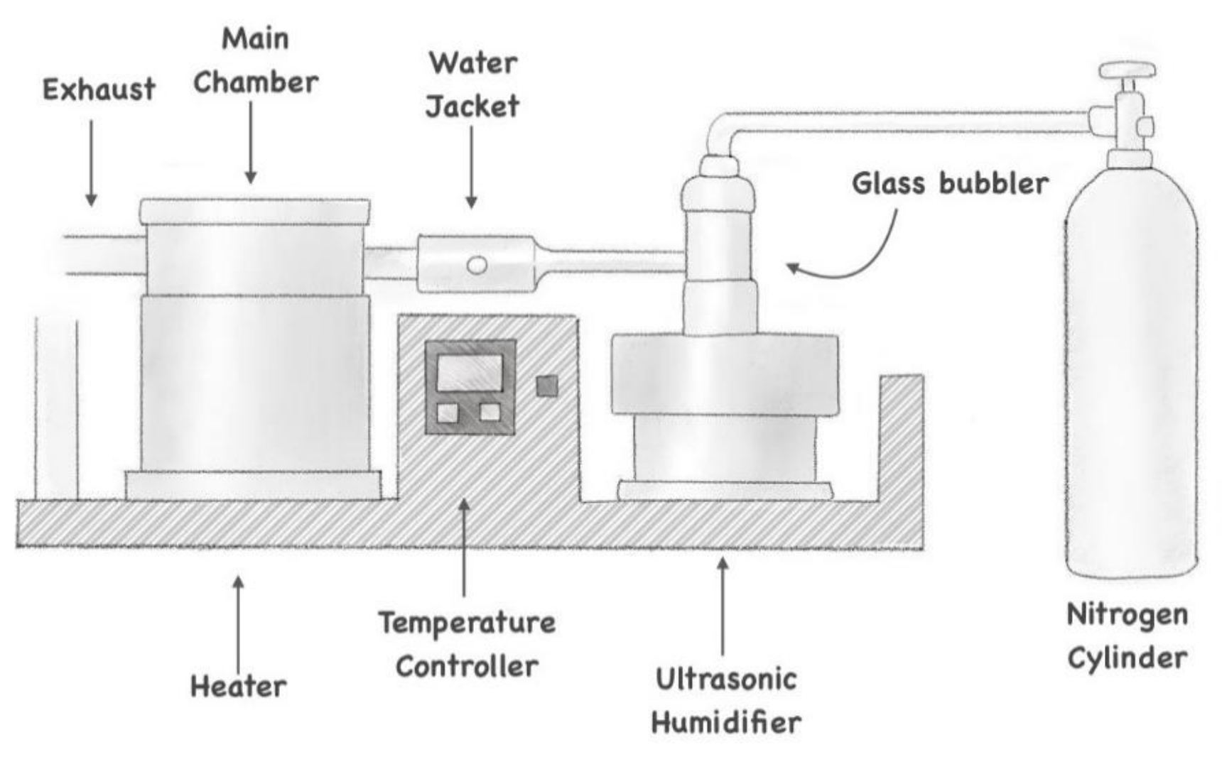
Figure 2.
XRD of pure MnO2, pure WO3 and WO3/MnO2 heterojunction thin film produced by AACVD deposited onto FTO at 400 ᵒC.
Figure 2.
XRD of pure MnO2, pure WO3 and WO3/MnO2 heterojunction thin film produced by AACVD deposited onto FTO at 400 ᵒC.
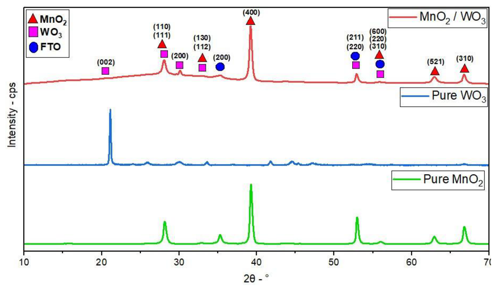
Figure 3.
SEM images of (a) pure WO3, (b) pure MnO2 (c) WO3/MnO2 and (d) EDS spectrum of WO3/MnO2 thin film produced by AACVD deposited onto FTO at 400 ᵒC.
Figure 3.
SEM images of (a) pure WO3, (b) pure MnO2 (c) WO3/MnO2 and (d) EDS spectrum of WO3/MnO2 thin film produced by AACVD deposited onto FTO at 400 ᵒC.
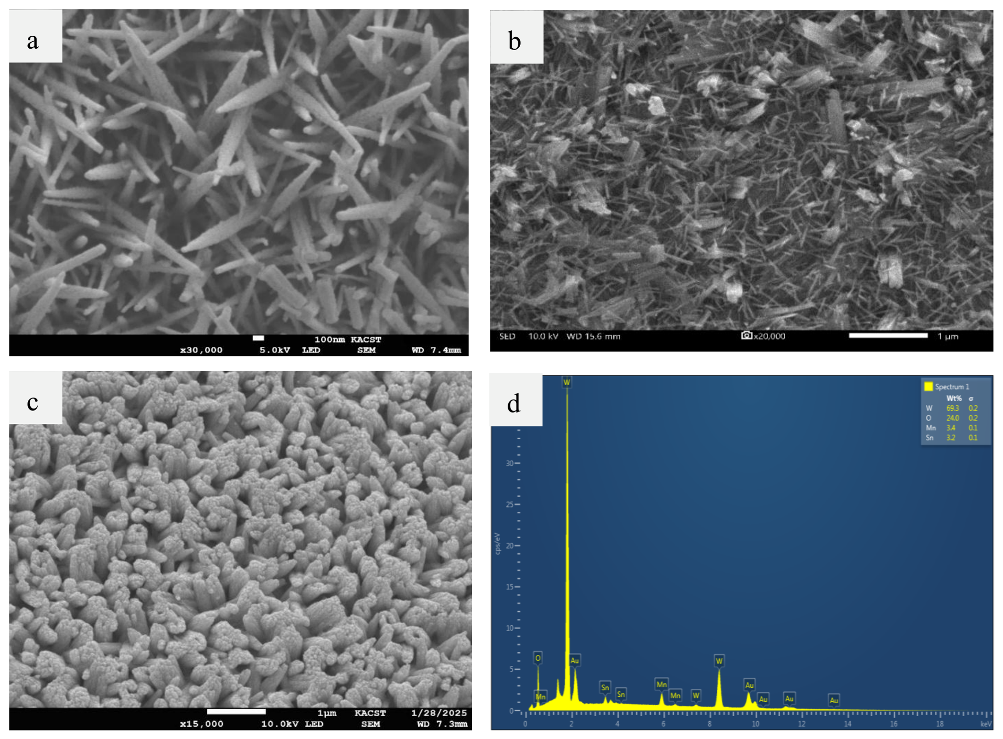
Figure 4.
SEM mapping for WO3/MnO2 thin films produced by AACVD deposited onto FTO at 400 ᵒC.
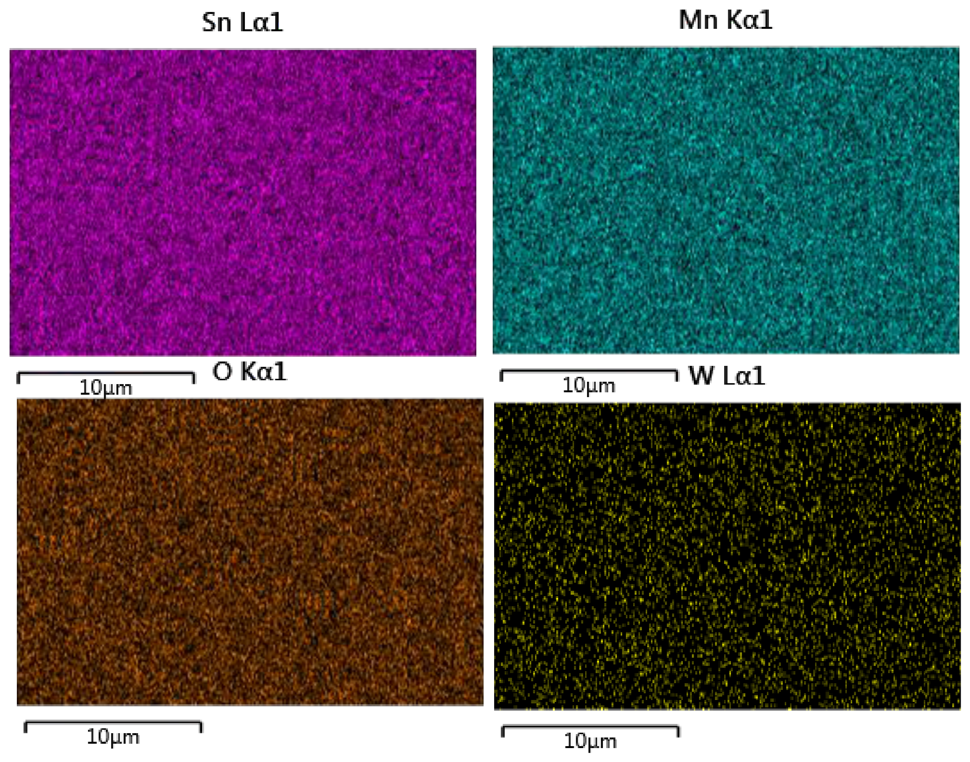
Figure 5.
AFM images of (a and b) pure MnO2, (c and d) pure WO3 and (e and f) WO3/MnO2 thin film produced by AACVD deposited onto FTO at 400 ᵒC.
Figure 5.
AFM images of (a and b) pure MnO2, (c and d) pure WO3 and (e and f) WO3/MnO2 thin film produced by AACVD deposited onto FTO at 400 ᵒC.
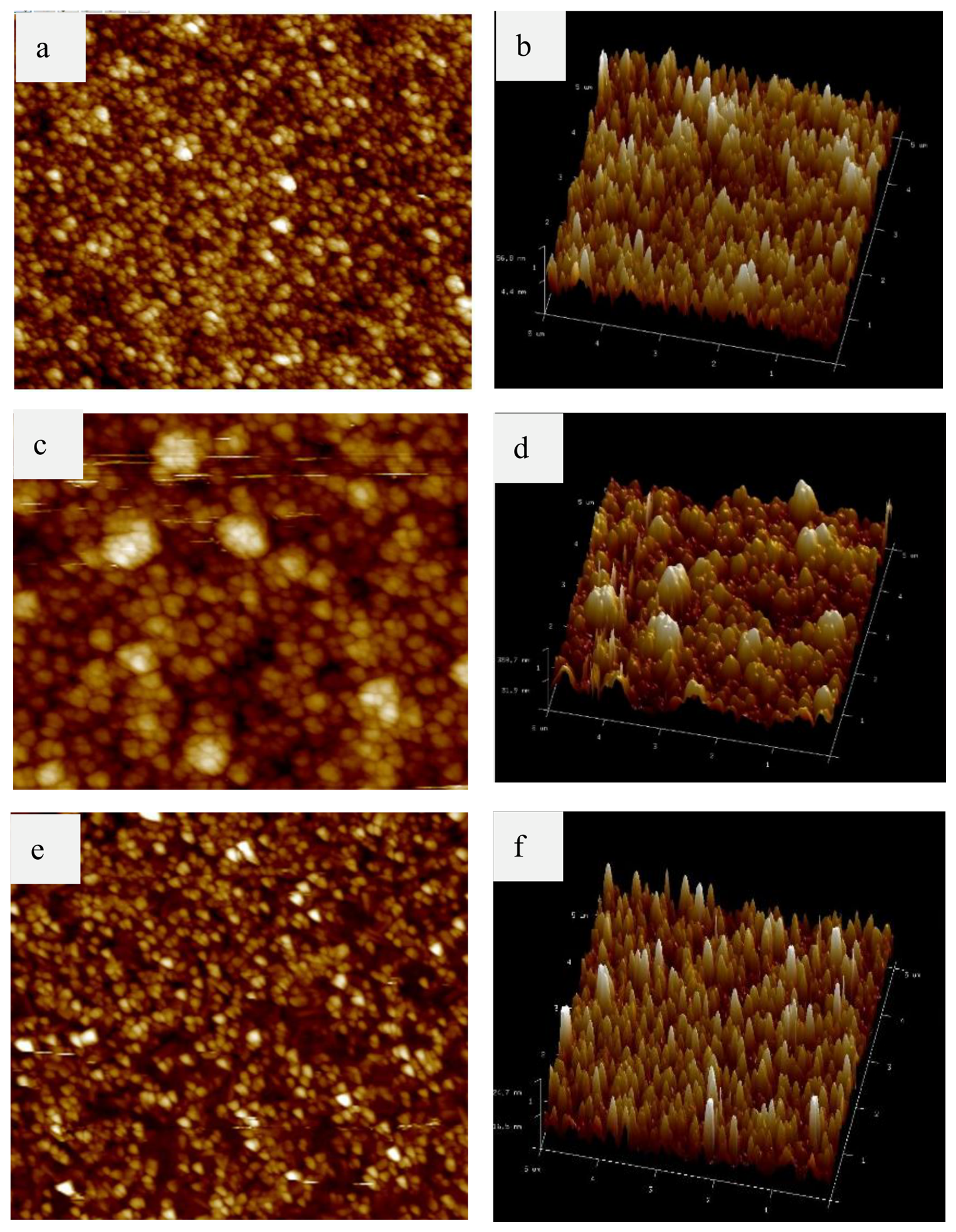
Figure 6.
The absorbance of (a) pure WO3 and (b) WO3/MnO2 thin films and Tauc plot of (c) pure WO3 and (d) WO3/MnO2 representing the values of energy band gap (Eg) for produced thin films by AACVD deposited onto FTO at 400 ᵒC.
Figure 6.
The absorbance of (a) pure WO3 and (b) WO3/MnO2 thin films and Tauc plot of (c) pure WO3 and (d) WO3/MnO2 representing the values of energy band gap (Eg) for produced thin films by AACVD deposited onto FTO at 400 ᵒC.
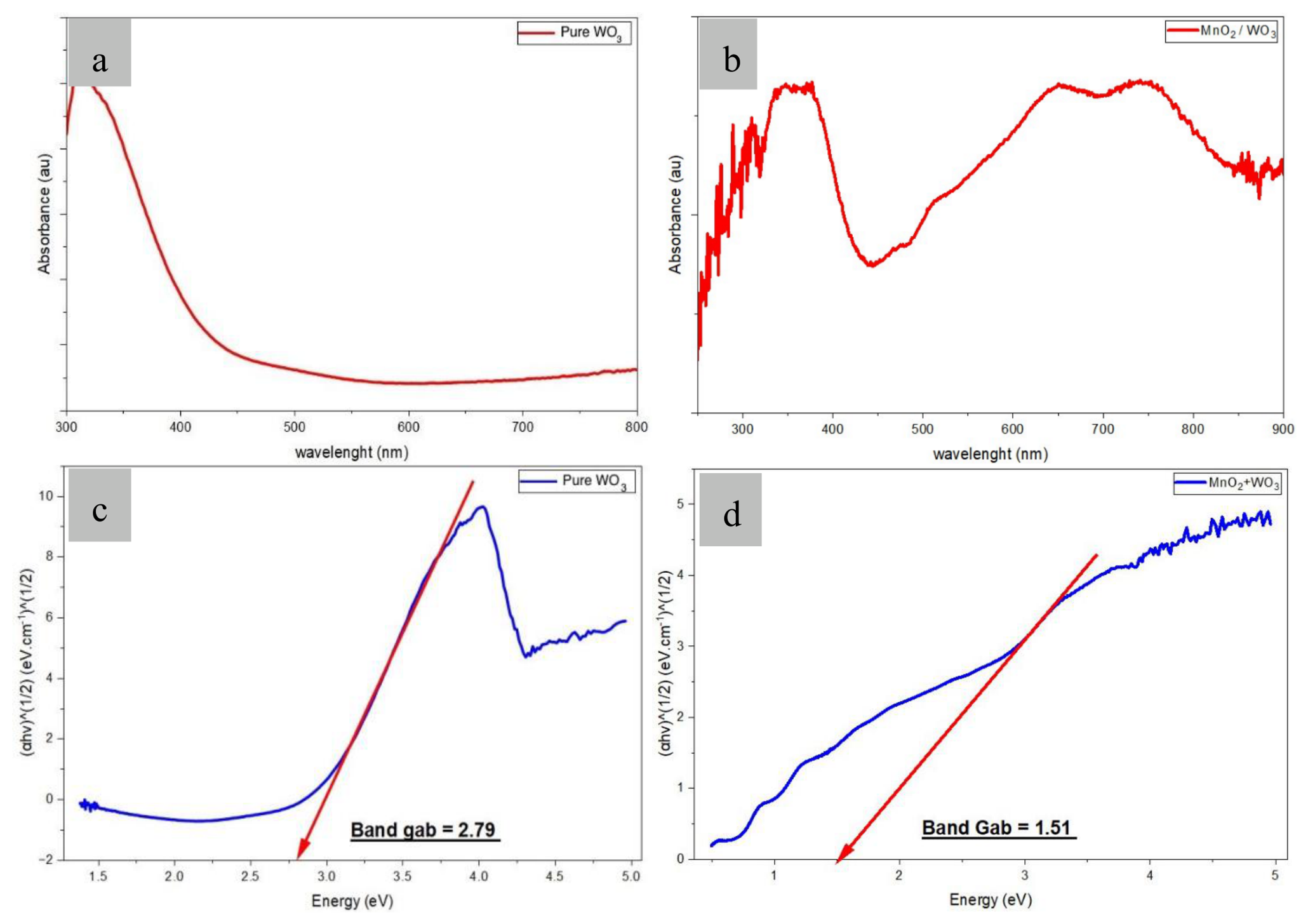
Figure 7.
PL of pure MnO2, pure WO3 and WO3/MnO₂ thin films produced by AACVD deposited onto FTO at 400 ᵒC.
Figure 7.
PL of pure MnO2, pure WO3 and WO3/MnO₂ thin films produced by AACVD deposited onto FTO at 400 ᵒC.
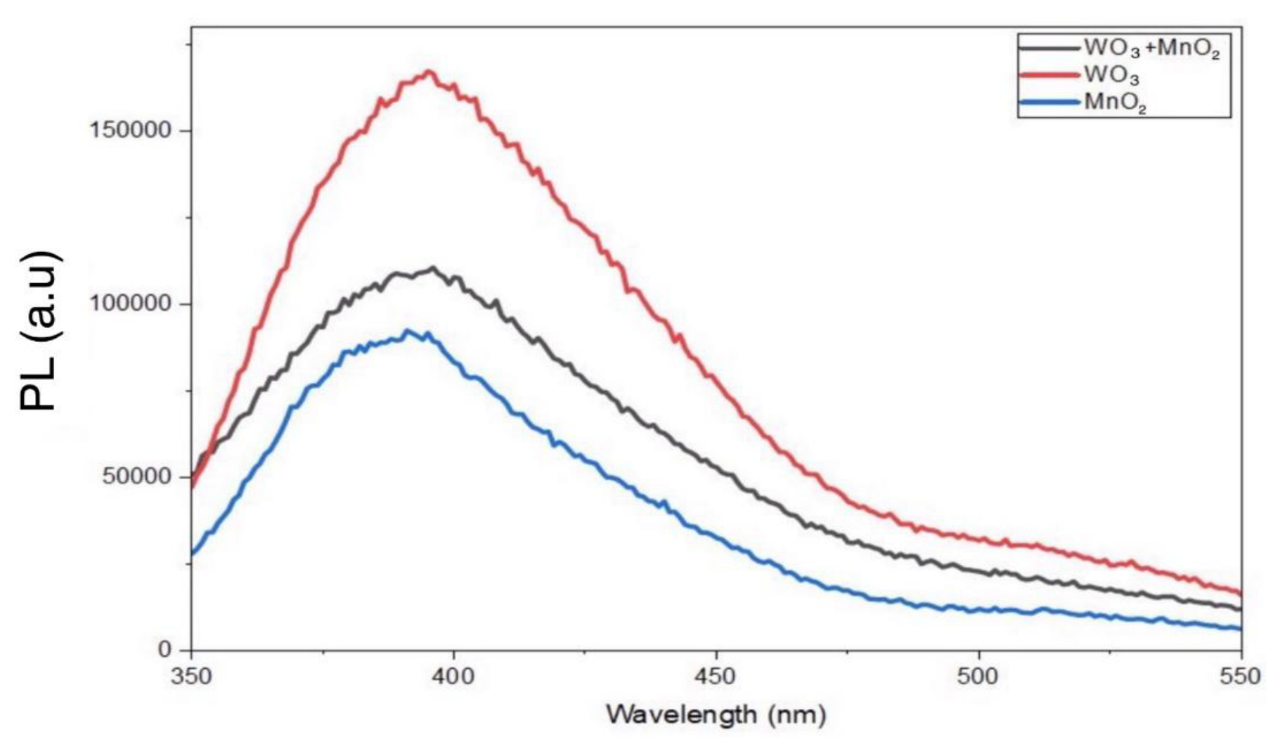
Figure 8.
Linear sweep voltammetry (LSV) of pure (a) MnO2, (b) pure WO3 and (c) WO3/MnO2 thin films as photoelectrons in 1.0 M KOH, and Mott –Schottky plots for three electrodes under simulated solar illumination (100 mW/cm2), using (d) pure MnO2, (e) pure WO3 and (f) WO3/MnO2 thin films as photoelectrons in 1.0 M KOH electrolyte. All films deposited onto FTO substrate using AACVD at 400 ᵒC.
Figure 8.
Linear sweep voltammetry (LSV) of pure (a) MnO2, (b) pure WO3 and (c) WO3/MnO2 thin films as photoelectrons in 1.0 M KOH, and Mott –Schottky plots for three electrodes under simulated solar illumination (100 mW/cm2), using (d) pure MnO2, (e) pure WO3 and (f) WO3/MnO2 thin films as photoelectrons in 1.0 M KOH electrolyte. All films deposited onto FTO substrate using AACVD at 400 ᵒC.
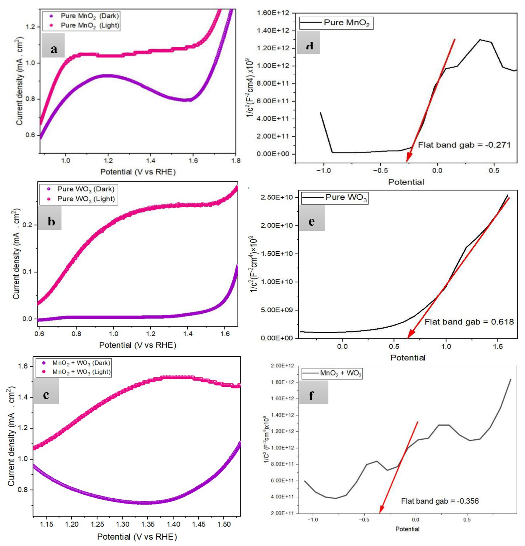
Figure 9.
Schematic representations depicting the mechanism of PEC water splitting in WO3/MnO2 heterojunction films on FTO substrates.
Figure 9.
Schematic representations depicting the mechanism of PEC water splitting in WO3/MnO2 heterojunction films on FTO substrates.
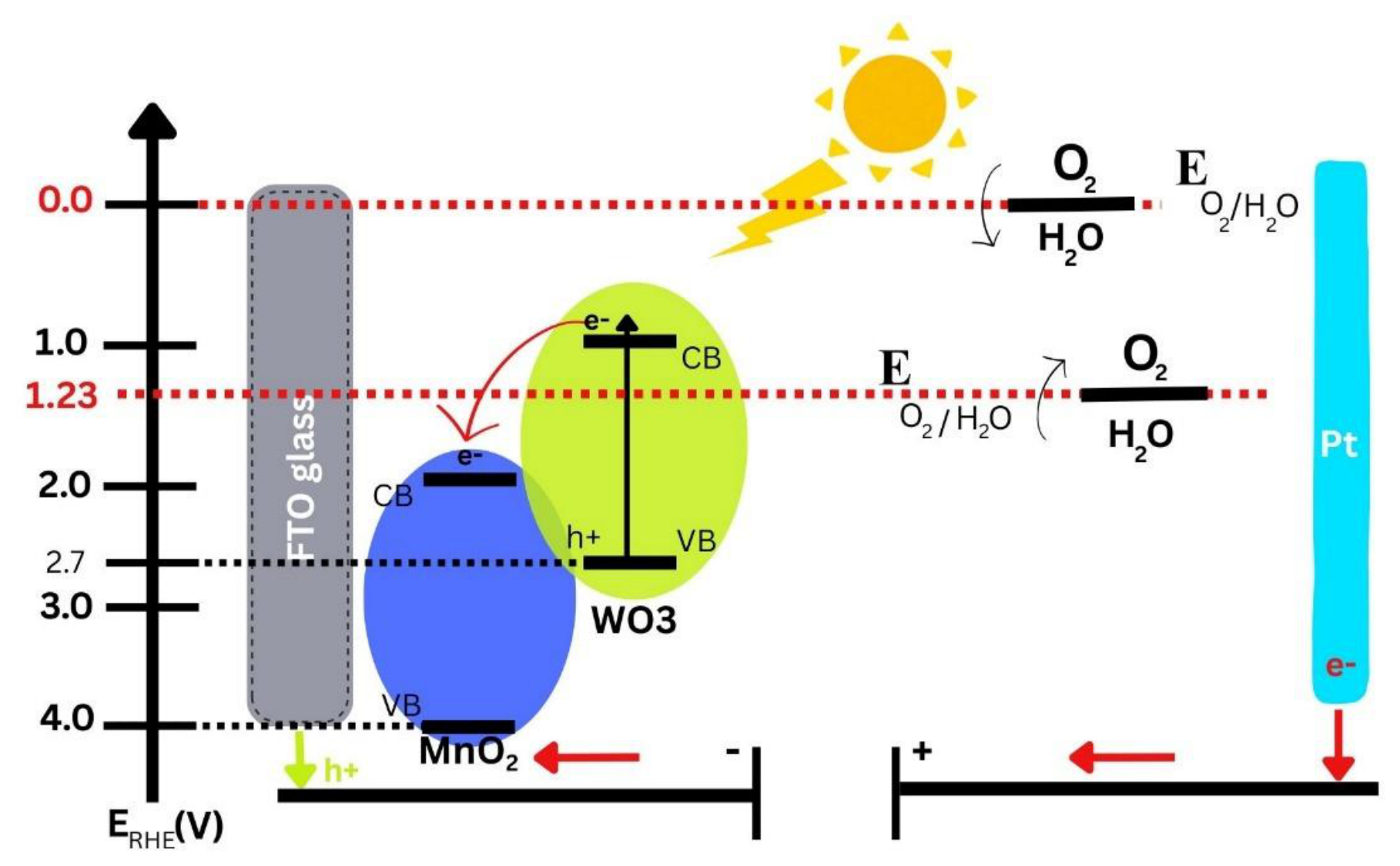

Table 1.
AFM measurements for pure MnO2, pure WO3 and WO3/MnO2 thin films produced by AACVD deposited onto FTO at 400 ᵒC.
Table 1.
AFM measurements for pure MnO2, pure WO3 and WO3/MnO2 thin films produced by AACVD deposited onto FTO at 400 ᵒC.
| Sample | Surface area μm2 |
Ra nm |
Rq nm |
|---|---|---|---|
| Pure MnO2 | 27.97 | 13.0 | 16.3 |
| Pure WO3 | 43.55 | 68.8 | 88.4 |
| WO3/MnO2 | 33.14 | 24.8 | 31.3 |
Disclaimer/Publisher’s Note: The statements, opinions and data contained in all publications are solely those of the individual author(s) and contributor(s) and not of MDPI and/or the editor(s). MDPI and/or the editor(s) disclaim responsibility for any injury to people or property resulting from any ideas, methods, instructions or products referred to in the content. |
© 2026 by the authors. Licensee MDPI, Basel, Switzerland. This article is an open access article distributed under the terms and conditions of the Creative Commons Attribution (CC BY) license (http://creativecommons.org/licenses/by/4.0/).
Copyright: This open access article is published under a Creative Commons CC BY 4.0 license, which permit the free download, distribution, and reuse, provided that the author and preprint are cited in any reuse.