

Submitted:
02 June 2026
Posted:
04 June 2026
You are already at the latest version
Abstract
Electrically small antennas (ESAs) relying on piezo-electric microelectromechanical-systems (MEMS) devices have attracted significant interest because they can deliver higher gains than conventional chip-scale antennas of comparable size. Most of the prior demonstrations for these ESAs rely on magnetostrictive (MS) thin films — soft ferromagnetic layers deposited using fabrication steps not performable in commercial foundries. Here, we propose an alternative ESA architecture that achieves a significant gain enhancement and excellent impedance matching to 50 Ω without requiring a MS layer. The architecture leverages an RF MEMS piezoelectric transformer (TRX) to enhance the intrinsic gain of a chip-scale radiator formed by an array of electrically small slot antennas. By providing passive voltage amplification, the transformer increases the tangential electric field in each slot and, consequently, the array’s equivalent magnetic-dipole moment, which scales with the square of the transformer’s voltage gain. To evaluate the performance improvement and validate the operating principle of the proposed ESA architecture, we built its first prototype on a YZ 0° X-cut LiNbO3 substrate. The prototype, manufactured using a single-mask microfabrication process, operates at 425 MHz and monolithically integrates a shear-horizontal (SH0) leaky surface acoustic wave (LSAW) transformer with a two-slot array. Its experimental characterization shows a maximum realized gain of -12.7 dBi. This gain value agrees with the value predicted by a simulation framework also presented in this work. Our findings pave the way toward future wireless tags for Internet-of-Things applications that combine chip-scale miniaturization with a scalable, single-lithography-step fabrication process compatible with the one commercially used to mass-produce RF Surface Acoustic Wave (SAW) filters.
Keywords:
electrically small antennas
; microelectromechanical systems
; YZ 0° X-cut bulk LiNbO3
; piezoelectric transformers
; monolithic integration
1. Introduction
The rapid expansion of the Internet of Things (IoT) continues to drive a demand for antennas that can be integrated into increasingly compact systems [1,2,3]. Fortunately, IoT links often tolerate reduced data rates in favor of a longer battery lifetime for wireless devices [4]. This enables the use of electrically small antennas (ESAs) in wireless sensor nodes [5,6,7,8]. Yet, using ESAs in wireless devices often yields reduced read range and increased bit-error-rate (BER) due to the ESAs’ low realized gain (). In practice, this low gain stems from the inability of matching the very small radiation resistance of ESAs to with conventional lumped components (i.e., inductors and capacitors) without introducing significant ohmic losses [9,10].
Motivated by this limitation and by the prospect of achieving chip-scale radiofrequency identification (RFID) tags operating in the Ultra-High-Frequency (UHF) range, a significant attention has been paid over the past decade to alternative electrically small antenna systems. Among them, those based on piezoelectric radio-frequency (RF) microelectromechanical systems (MEMS)-based devices have attracted particular interest because they can transform ESAs’ radiation impedances to without resorting to lossy inductors and capacitors. Currently, the most pursued RF MEMS-based approach for this purpose focuses on RF magnetoelectric (ME) antennas [11]. These devices, operating in the RF range, embed magnetostrictive (MS) thin films within RF MEMS bulk acoustic wave (BAW) [12,13,14] or surface acoustic wave (SAW) resonators [15,16]. Most RF ME antennas reported to date rely on RF MEMS devices based on Aluminum Nitride (AlN) or Aluminum Scandium Nitride (AlScN), with the latter enabling larger fractional bandwidths than AlN for the same device size [14]. These ESAs exploit the large strain generated when an RF MEMS device is driven at its mechanical resonance frequency to dynamically modulate the magnetization of the embedded MS layer, which enables intrinsic gains () orders of magnitude higher than those achievable by solely relying on the oscillating electric dipole moment generated by the piezoelectric layer. Moreover, exploiting an acoustic vibration mode naturally provides a pathway to excellent matching to without the need for lossy electronic lumped components. Altogether, these features enable RF ME antennas to achieve two orders of magnitude higher than those of conventional ESAs with comparable dimensions [11]. However, RF MEMS-based ME antennas require the integration of an MS layer, which complicates their fabrication in conventional RF MEMS foundries [17,18,19] and poses a major obstacle to scaling RF ME antenna technology toward large-scale manufacturing. For this reason, researchers have looked for alternative RF MEMS-based ESAs not relying on MS layers.
Recently, a new class of acoustically mediated piezoelectric (AMP) antennas has been reported [20,21,22]. Among them, in 2025, an RF MEMS-based ESA was presented, wherein a Rayleigh wave resonator built on a Y-cut substrate and fed using an asymmetrical ground-signal-pad structure has shown the ability to boost in an on-chip electrical dipole antenna by enabling improved matching to [21]. While this seminal demonstration has certainly paved a new pathway for RF MEMS devices to enable ESAs with higher than conventional electromagnetic counterparts without requiring MS layers, the device reported in [21] sees its performance limited by the low of the electrical dipole. Also, in its current form, it still shows modest matching to (it does not present a quantifiable -10 dB fractional bandwidth).
In this work, we report an alternative RF-MEMS-based ESA architecture with improved and smaller form factor than the previous AMP ESA in [21]. The reported architecture consists of a monolithically integrated RF MEMS piezoelectric transformer (TRX) driving an array of two ESAs. The TRX has two purposes: (1) enable good matching to and (2) provide a passive voltage amplification that effectively increases for the slot-array compared to what the slot-array achieves when connected directly to a source. From now on, we will refer to this system as TRX-ESA.
We also describe the first prototype of this architecture, built on a YZ X-cut substrate through a single-step lithographic fabrication process. The TRX-ESA prototype, operating at 425 MHz and relying on a shear-horizontal () mode transduced by a leaky surface acoustic wave (LSAW) TRX [23,24,25], shows a of -12.7 dBi, which, to the best of our knowledge, represents the highest gain ever recorded for RF MEMS-based ESAs. Such measured gain level closely matches the value we predicted using a simulation framework that we also present for the first time in this work. Our prototype also shows a large -10 dB bandwidth and greatly improved return loss compared to the previous AMP ESA in [21], thanks to the large electromechanical coupling coefficient () of the TRX device.
In the next sections, we describe the principle of operation of the reported TRX-ESA system, the simulation framework we developed to predict its achievable performance, and a study of the impact of the TRX’s quality factor (Q) and on the highest achievable gain enhancement. Next, we report on the design of the LSAW device, followed by a discussion on the measured performance of the TRX-ESA prototype designed and built in this work.
2. Principle of Operation
The TRX-ESA presented in this work comprises two on-chip slot antennas on a YZ X-cut substrate, driven by the output voltage of a UHF -mode LSAW piezoelectric transformer (TRX). The TRX is designed to maximize at a target frequency (). A top-view schematic of the TRX-ESA system, along with its in-plane dimensions, is reported in Figure 1. In the next subsections, we first examine the intrinsic radiation characteristics of the slot array using numerical and analytical methods. We then clarify the role of the LSAW device and show that its inclusion enhances both and for the slot array by acting as a piezoelectric transformer [26]. This is done first through a simplified analytical model and then through actual circuit simulations capturing more realistic electromechanical and RF models for the TRX-ESA prototype reported in this work.
2.1. Intrinsic Radiation Characteristics of the Array of Slots
The slot array integrated into the reported TRX-ESA system consists of two electrically small rectangular slots, which are created by opening two gaps in the metallic pad structure normally used to test an LSAW device with a ground–signal–ground (GSG) probe (Figure 1). Each slot has a width () of , accounting for the presence of lateral fringing fields, and a gap () of , resulting in an aperture area per slot () equal to and in an estimated capacitance of the slot () of . Moving forward, we will model the underside of the wafer as being backed by a metallic plane acting as a perfect electric conductor (PEC). This assumption reflects our measurement conditions, where the TRX-ESA system operates in close proximity to a conductor (i.e., the metallic chuck of our probe-station).
Following the standard aperture-antenna formalism, we analyze the radiation from each slot by defining an equivalent bounded volume (V) consisting of the slab within the slot’s aperture. By applying the equivalence principle [27], the tangential component of the electric field across each side of the slab can be replaced by an equivalent magnetic current density. Since the electric field in each slot, , is mainly oriented along and (i.e., the z-component of is negligible) and since we are assuming the presence of a PEC under the chip, the only equivalent magnetic current density that can contribute to the far field radiation is the one corresponding to the top surface of V. This magnetic current density has components along and with magnitude proportional to the magnitude of the components along (i.e., ) and (i.e., ) respectively. Now, since the reported TRX-ESA system is symmetric along the y-axis (Figure 1), the equivalent magnetic current densities along for the two slots are equal in magnitude but shifted by in phase. This implies that their contribution to the far-field power radiated can be neglected. Consequently, we retain only the x-component of the equivalent magnetic current density for the top surface of each slot, shown in Eq. (1).
The factor “2” in Eq. (1) comes from the image theorem [27] (i.e., the TRX-ESA system operates above a PEC). For best accuracy, we extract for different input voltages () applied to the signal pad of our GSG probing area directly from finite element analysis (FEM) simulations. To this end, we consider an ad-hoc simulated geometry in which the LSAW TRX is electrically replaced by an ideal short. Next, we simulate in each slot for a equal to 1 V (see Figure 2) and compute its spatial average () over the slot area. This allows us to approximate as [Eq. (2)]:
For each slot, we can then compute an equivalent magnetic moment () as [Eq. (3)]:
where is obtained by substituting Eq. (2) into Eq. (1). In Eq. (3), is the angular frequency and is the permeability of free space. Given Eq. (2) and the specific slot geometry, can be found to be approximately .
Since the two slots are electrically small, have identical equivalent magnetic current densities, and are separated by a distance (with being the electromagnetic wavelength), their contributions add coherently (in phase). Therefore, the equivalent magnetic dipole moment of the two-slot array () becomes:
We can now use the Larmor formula to compute the far-field power radiated in free space () by an electrically small magnetic dipole with moment [Eq. (5)] [27].
In Eq. (5), is the free-space wave impedance and is the free-space wavenumber. It is important to emphasize that is proportional to . Moreover, (and consequently ) is largely independent of for and grows linearly with , as reported in Figure 3 and Figure 4, respectively. This leads to an important design consideration: for a fixed , increasing requires using larger values, which can be achieved with minimal changes of by simultaneously increasing . As will be clear later, the ability to increase without varying permits to decouple the slot design from the design of the TRX, whose achievable voltage gain () depends heavily on .
Determining is the first step required to find the radiation efficiency () of the slot array. The second and last step consists in computing the power absorbed () by the two slots under ideal matching to a reference terminal impedance (), here set to . Under these conditions, coincides with the available power of a generator with Thevenin voltage equal to . Its value is reported for completeness in Eq. (6).
Eqs. (5)–(6) can now be used to compute as [Eq. (7)]:
It is worth mentioning that is independent of . By using the expression of in Eq. (4), we can estimate for =2 to be approximately (i.e., on a logarithmic scale).
The calculated value can now be used to quantify for the slot array at the targeted frequency of operation (i.e., for ). To do so, we use the expression reported in Eq. (8).
In Eq. (8), D is the slot array’s directivity, which can be estimated to be six (i.e., four times the directivity of an electrically small dipole). This directivity value considers the presence of two slots operating in close vicinity to a metallic ground plane parallel to the slots’ aperture.
2.2. Impact of the Piezoelectric Transformer on Realized and Intrinsic Gains
Having determined the intrinsic radiation characteristics of the slot array, we move on to quantify the impact of the LSAW TRX on and . We focus on two key figures of merit: the matching efficiency, , between a source and the TRX-ESA system, and (i.e., the voltage gain achievable when the LSAW device is terminated by a load capacitance, , equal to 2). Together, and set the maximum attainable values of and for the TRX-ESA system reported in this work.
We first derive and analytically by modeling the reported TRX-ESA system with the LSAW device’s Butterworth–Van Dyke (BVD) equivalent circuit [28] terminated by , as reported in Figure 5.
Later, in Section IV, we will extract the same metrics directly from circuit simulations when using the Modified Butterworth–Van Dyke (MBVD) model rather than the BVD model [29]. This allows to more accurately capture the operation of the actual LSAW device embedded in the prototype we built for this work. It is also worth pointing out that the two slots can be modeled by only using , because the slots’ radiation resistance (in the m-range) is too small to have a significant impact on the achievable and .
2.2.1. Calculation of
is defined as the fraction of the source’s available power that is delivered to the TRX-ESA system. For its analytical derivation, we represent the LSAW TRX in terms of the total admittance of its BVD equivalent circuit, [30]. is the parallel combination of the LSAW device’s motional branch—described by the complex impedance [Eq. (9)] (or, equivalently, by the admittance [Eq. (10)])—and the device’s static capacitance , with admittance .
In Eqs. (9)–(10), , , and denote the motional resistance, motional inductance, and motional capacitance, respectively. For any MEMS transformer with resonance angular frequency =, quality factor Q, static capacitance , and electromechanical coupling coefficient [31,32,33], these parameters are given by Eqs. (11)–(13):
can be written as [Eq. (14)]:
Eq. (14) can thus be rewritten by substituting Eq. (10) into Eq. (14) and then replacing , , and with their expressions from Eqs. (11)–(13). This yields the expression for in Eq. (15):
Next, we compute the return loss of the whole TRX-ESA system, which is equivalent to the of the LSAW device when terminated on the total capacitance of the slot-array (=2, see Figure 5). To this end, we can write the TRX-ESA system’s input reflection coefficient (i.e., its ) as [Eq. (16)]:
where is the reference admittance and is the TRX-ESA system’s input admittance (Figure 5); with regards to , we use , in line with what is typically done for -matched electronic components. can be computed as shown in Eq. (17), where =.
Its complete, fully developed expression is reported in Eq. (18). We can now use the computed expression for to evaluate the of the circuit in Figure 5 via Eq. (16). Then, from the computed , we can calculate via Eq. (19).
As a numerical example, Figure 6 reports as a function of and of the TRX’s resonance frequency (i.e., ), evaluated at when using experimentally extracted parameters for the LSAW device (i.e., and ) (refer to Section IV for more information on our experimental data). Evidently, the maximum value occurs when the LSAW transformer is designed with a value slightly below . This trend is expected because a capacitive load produces a stiffening effect that shifts the resonance of upward, with a shift proportional to and inversely proportional to [34,35]. Accordingly, selecting a slightly lower maximizes for .
2.2.2. Calculation of
Having completed the extraction of , we now turn to the extraction of . To this end, we analyze the two-port network in Figure 7, which includes the input generator’s reference impedance, . This formulation is convenient because can be obtained directly from the coefficients of the network’s Y-matrix reported in Eq. (20).
The complete, fully-developed expression for is reported in Eq. (21). From Eq. (20), we can compute as [Eq. (22)]:
We also show the extended derivation for as a function of in Eq. (23). As we did for in Figure 6, Figure 8 reports , numerically evaluated for as a function of and , when assuming the same Q and of the LSAW device in our built prototype (as we will discuss in Section IV). Evidently, a equal to maximizes , which is found to be 6.51. This voltage amplification arises because a two-port LSAW resonator, even with identical transducer geometries at both ports, behaves as a TRX when one port is terminated with a capacitive load [26]. Thus, the LSAW device can passively step-up the voltage level applied at its input port. Such step-up increases relative to the case without the LSAW device and, consequently, increases the radiated power by a factor equal to . In other words, the radiated power of the slot array is significantly enhanced when the array is driven through a TRX rather than being directly connected to a power source.
This enhancement can be interpreted as a boost in the slot array’s radiation efficiency: increases the electric-field distribution across the slots and, consequently, increases . An expression of the power radiated by the slot-array when using a TRX to drive it () is reported in Eq. (24), followed by the corresponding modified expression for the radiation efficiency () in Eq. (25).
Evidently, both the power radiated and the radiation efficiency of the slot-array are enhanced by a factor equal to when driven by a piezoelectric transformer.
2.2.3. Calculation of
Having determined both and , we are now ready to compute , which we can do by using the following equation [27]:
where
Evidently, is proportional not only to , as expected, but also to . It is worth emphasizing that, for any targeted operating frequency, and are maximized for different combinations of and values. It is therefore important to numerically identify the optimal and values to maximize . As an example, Figure 9 reports , numerically computed under the same assumptions used to generate Figure 6 and Figure 8. Evidently, an LSAW device with =425 MHz and a close to is ideal for maximizing at . The maximum value identified in this study shows that the adoption of an optimized design for the TRX can lead to a almost 36 times larger than , hence enabling a strong improvement of over when considering the actual slot-array geometry used in this work. Such optimal operating conditions correspond to a value equal to 0.8, thus approaching ideal matching conditions. Finally, we report a vs. frequency trend extracted using the analytical model discussed across this Section in Figure 10, along with the trend of for the slot-array when no TRX is used. Evidently, our reported TRX-ESA architecture enables a large boost of compared to when operating in the proximity of the resonance frequency of , allowing us to estimate a maximum gain of -15.9 dBi at . As mentioned earlier, is different from because of the presence of stiffening the TRX.
2.2.4. Impact of Q and on
It is also useful to study how the gain enhancement brought by the adoption of the TRX is related to its electromechanical performance. To do so, we conducted an additional analytical investigation where we searched for the maximum value for varying Q and values. The results of this analysis are plotted in Figure 11. Evidently, both the increases in Q and generally lead to enhanced values. However, beyond certain Q and values, a plateau emerges in the achievable enhancement, with a maximum value still attained for approaching . Our study also finds that adopting much smaller values [i.e., values for which ] can yield substantially larger when the slots are designed such that approaches , as reported in Figure 12. Consequently, can amplify the sensitivity of to increases in compared to the quadratic dependence on exhibited by . To this end, the weak dependence of on makes it possible to reduce by increasing without reducing at the same time. It is also worth pointing out that the enhancement in attained by using the TRX inevitably comes with a reduced fractional bandwidth. Finally, we note that we did not pursue low- designs in this work. Although such designs could yield higher , the optimal TRX (with approaching ) would be substantially smaller than the device we fabricated. This size reduction would likely increase the mismatch between the measured and simulated LSAW resonance frequency (see Section III) and could also add more spurious modes and reduce Q (i.e., a smaller active region typically leads to larger anchor dissipations compared with larger-area devices [36]).
3. LSAW TRX Design and Optimization
As mentioned earlier, the LSAW TRX was fabricated on a bulk YZ X-cut substrate. The choice of this cut allows to excites the -mode, which is characterized by an in-plane displacement perpendicular to the wave propagation direction, as confirmed by FEM simulations (Figure 13a). This mode exhibits an inherently large [25,37], making the proposed LSAW architecture highly attractive for achieving large and, consequently, strong enhancements in of chip-scale slot-arrays. Yet, the highly dispersive nature of the modes exploited by LSAW devices implies that the strongly depends on , with being the thickness of the metal electrodes and the acoustic wavelength. Since the associated mass loading concentrates the acoustic energy beneath the surface and reduces substrate leakage, denser electrode materials are preferred [38]. In this work, we select Gold (Au) as metal, as it offers an optimal combination between high density and low electrical resistivity, which minimizes the ohmic loading of the transducer [25]. In the limit of very thin electrodes (), the acoustic field is poorly confined beneath the interdigitated transducer electrodes (IDTs), resulting in significant energy leakage into the substrate. However, as increases, the acoustic energy is progressively concentrated in the region near the surface, improving .
To identify the optimal electrode thickness for the present design, we performed 3D FEM simulations on a unit cell of the YZ X-cut substrate with a pair of its Au IDTs. We used a section with thickness beneath the electrodes to approximate the semi-infinite bulk substrate, with periodic boundary conditions applied along the propagation direction of the acoustic wave and a perfectly matched layer (PML) at the bottom of the substrate, in order to absorb bulk-radiated energy. We simulate the behavior of as function of the ratio of the metal in Figure 13b. As evident, can be maximized when working at ratios between 0.025 and 0.05. For this reason, we designed our TRX with a ratio of 0.0375, aiming to a close to 35%.
The finalized TRX consists of 20 pairs of gold IDTs surrounded by electrically grounded reflectors, and the aperture of the IDTs is set to m for impedance matching purposes. The of the LSAW TRX is set by the IDT period , according to:
where is the phase velocity of the LSAW mode on X-cut . This term depends on the electrode material, on its thickness and on the chosen ratio, and can be obtained from FEM simulations.
4. Experimental Section
4.1. Fabrication Process
The one-mask fabrication process of the LSAW TRX is illustrated in Figure 14a. A 300 nm thick layer of Au was deposited on a YZ 0° X-cut wafer through e-beam evaporation. Subsequently, the Au-coated wafer was patterned via UV-photolithography and an ion beam etching (IBE) process to minimize fencing effects on the edges of the electrodes. The wafer was then diced in chips, from which we finally sub-diced a 2.5 by 2.5 mm chip hosting the fabricated TRX-ESA. Figure 14b,c show an optical micrograph of the chip hosting the device and a scanning electron microscope (SEM) close-up picture of the TRX’s IDT region. We could not acquire a single SEM image of the full device, because the charging effects under electron-beam exposure on bulk become prohibitive when imaging the entire chip area [39].
4.2. S-Parameters Characterization and MBVD Fitting
The fabricated TRX-ESA was characterized through on-chip S-parameter measurements using a Keysight N5221A Vector Network Analyzer and a m-pitch GSG probe. The measured response around the LSAW is reported in Figure 15. As evident, the TRX-ESA shows a good impedance matching at 425 MHz, showcasing a maximum return loss of 23 dB and a -10 dB bandwidth of 0.53%.
The measured vs. frequency trend was fitted by using a two-mode MBVD model [40]. The retrieved from our MBVD fitting is superimposed to the measured one in Figure 15. It is important to point out that the MBVD model used here considers an additional mode beyond the main one to better match the behavior. Also, the model considers two additional resistances ( and ) and a capacitor (). and capture the effect of the ohmic losses in the IDT and GSG probing pads, as well as dielectric dissipations in the film. , on the other hand, models the capacitance between the slots’ top metal strips and the signal pad. A schematic representation of the final MBVD circuit we used to match the measured response is reported in the inset of Figure 15. The various MBVD parameters that best fit the measured electrical response of our reported TRX-ESA system are reported in the caption of Figure 15. The fitted for the main mode of our LSAW TRX is .
Using the extracted MBVD parameters, we retrieved the experimental values of and , and computed based on the simulated of the slots. As seen in Figure 10, we expect a maximum of -15.9 dBi. This value is achieved at a frequency that is higher than due to the stiffening effect produced by .
4.3. Experimental Characterization of and Comparison with Other RF-MEMS ESA Systems
The value of for the fabricated TRX-ESA system was measured using the gain-comparison method [12,27]. The experimental setup for gain extraction is illustrated in Figure 16. We first placed a transmitting Log Periodic antenna (Aaronia HyperLOG® 4025) at a fixed distance from the device under test, and connected it to port 1 of the VNA. Port 2 was connected to the on-chip TRX-ESA via GSG probes. Then, we replaced the on-chip device with a reference antenna with fully characterized gain, . was computed as follows:
In Eq. (29), and are the transmission coefficients in linear scale measured with the TRX-ESA system and the reference antenna in place, respectively.
The resulting trend versus frequency is reported in Figure 17. We measured a maximum gain of -12.7 dBi, which, to the best of our knowledge, is the highest gain ever reported for RF MEMS based ESAs, and is in close agreement with the prediction of our analytical model shown in Figure 10. We believe that the ∼3 dB discrepancy between measured and analytically predicted gain values arises from slight underestimations of , which may stem from radiation contributions of secondary apertures, as well as from unmodelled variations in the dielectric characteristics of the substrate. In this regard, it is worth emphasizing that a 30% reduction of would be enough to cause an underestimation of (and consequently ) by 3 dB.
We finally compare the proposed TRX-ESA against previously reported on-chip antenna systems in Table 1. Our TRX-ESA architecture demonstrates exciting advantages across all key performance metrics. First, it shows a clear size reduction compared to its SAW-based counterparts in the same frequency range [15,21]. Even more importantly, the TRX-ESA architecture shows an improvement in the realized gain of approximately 4.5 dBi over the highest previously reported gain for an acoustically actuated device [21]. It is worth adding that the AMP-ESA reported in [21] operates at approximately the same frequency while being nearly two times larger in area, thus representing an ideal benchmark for our device. Our prototype also shows a -10 dB bandwidth of 0.53%.
Altogether, the high gain and wide fractional bandwidth of our TRX-ESA leads to a gain-bandwidth product of 28., which is almost an order of magnitude higher than the highest previously reported one for RF MEMS based ESAs [41].
5. Conclusion
In this work, we presented and experimentally characterized a TRX-ESA system, formed by the monolithic integration of an LSAW piezoelectric transformer with an ESA. The proposed architecture shows a significant gain enhancement, excellent impedance matching to and the highest gain-bandwidth product among previously demonstrated RF MEMS-based ESAs. The reported TRX-ESA architecture leverages for the first time the passive voltage amplification provided by an LSAW TRX, which increases the tangential electric field across an array of two slot antennas, thus boosting their radiated power and guaranteeing impedance matching despite their small electrical size. To model the acoustic and radiation behavior of the LSAW TRX, we built an ad-hoc simulation framework combining analytical and finite-element methods simulations, which reliably predicts the realized gain of the TRX-ESA system and provides a basis for design optimization.
Our findings demonstrate that monolithically integrated piezoelectric transformers offer a scalable and foundry-compatible route to UHF chip-scale ESAs with substantially improved performance, paving the way towards miniaturized passive wireless sensor tags for IoT applications.
Acknowledgments
We acknowledge the support of the National Science Foundation (NSF) under award No. 2414743.
References
- Khan, S.; Mazhar, T.; Shahzad, T.; Bibi, A.; Ahmad, W.; Khan, M.A.; Saeed, M.M.; Hamam, H. Antenna systems for IoT applications: a review. Discov. Sustain. 2024, 5, 412. [Google Scholar] [CrossRef]
- Jha, K.R.; Bukhari, B.; Singh, C.; Mishra, G.; Sharma, S.K. Compact planar multistandard MIMO antenna for IoT applications. IEEE Trans. Antennas Propag. 2018, 66, 3327–3336. [Google Scholar] [CrossRef]
- Wu, W.J.; Yin, Y.Z.; Zuo, S.L.; Zhang, Z.Y.; Xie, J.J. A new compact filter-antenna for modern wireless communication systems. IEEE Antennas Wirel. Propag. Lett. 2011, 10, 1131–1134. [Google Scholar] [CrossRef]
- Callebaut, G.; Leenders, G.; Van Mulders, J.; Ottoy, G.; De Strycker, L.; Van der Perre, L. The art of designing remote iot devices—technologies and strategies for a long battery life. Sensors 2021, 21, 913. [Google Scholar] [CrossRef]
- Peng, Q.; Zhang, C.; Zhao, X.; Sun, X.; Li, F.; Chen, H.; Wang, Z. A low-cost UHF RFID system with OCA tag for short-range communication. IEEE Trans. Ind. Electron. 2015, 62, 4455–4465. [Google Scholar] [CrossRef]
- Broutas, P.; Contopanagos, H.; Kyriakis-Bitzaros, E.D.; Tsoukalas, D.; Chatzandroulis, S. A low power RF harvester for a smart passive sensor tag with integrated antenna. Sens. Actuators A Phys. 2012, 176, 34–45. [Google Scholar] [CrossRef]
- Mugisha, A.J.; Rigi, A.; Tsiamis, A.; Podilchak, S.K.; Mitra, S. Electrically small antenna for RFID-based implantable medical sensor. IEEE J. Radio Freq. Identif. 2023, 7, 182–191. [Google Scholar] [CrossRef]
- Casilli, N.; Colombo, L.; Cassella, C. A UHF 1.3 cm 2 Passive Subharmonic Tag With a 13 m Read-Range. IEEE Microw. Wirel. Technol. Lett. 2023, 33, 939–942. [Google Scholar]
- Strachen, N.; Booske, J.; Behdad, N. Class-E, active electrically small antenna with enhanced bandwidth-efficiency product and high radiated power at the high-frequency (HF) band. J. Appl. Phys. 2024, 135. [Google Scholar]
- Hansen, R.C. Electrically small, superdirective, and superconducting antennas; John Wiley & Sons, 2006. [Google Scholar]
- Nan, T.; Lin, H.; Gao, Y.; Matyushov, A.; Yu, G.; Chen, H.; Sun, N.; Wei, S.; Wang, Z.; Li, M.; et al. Acoustically actuated ultra-compact NEMS magnetoelectric antennas. Nat. Commun. 2017, 8, 296. [Google Scholar] [CrossRef] [PubMed]
- Fu, Y.; Hu, R.; Li, J.; Li, D.; Song, Y.; Fang, B.; Lin, W.; Zeng, Z.; Zhu, X. XBAR-structured magnetoelectric antenna with magnetostrictive interdigital transducers. IEEE Electron Device Letters, 2025. [Google Scholar]
- Ma, M.; Chen, C.; Xu, H.; Liu, P.; Xiao, B.; Liang, S.; Fu, S.; Song, C.; Pan, F. High-frequency magnetoelectric antenna by acoustic excitation for 5G communication. IEEE Antennas Wirel. Propag. Lett. 2024, 23, 1518–1522. [Google Scholar] [CrossRef]
- Maietta, N.; Quaresima, S.; Liu, Y.; Kaya, O.; Dong, J.; Wu, M.; Zhang, X.; Cassella, C. Design, Multiphysics Modeling and Experimental Characterization of RF AlScN Magnetoelectric Antennas. 2026. [Google Scholar]
- Zhang, C.; Ji, Y.; Gu, H.; Zhang, P.; Liu, J.; Liang, X.; Yang, F.; Ren, T.; Nan, T. Surface acoustic wave actuated MEMS magnetoelectric antenna. IEEE Electron Device Lett. 2024, 45, 2009–2012. [Google Scholar] [CrossRef]
- Ma, M.; Chen, C.; Xu, H.; Cao, Y.; Han, L.; Xiao, B.; Liu, P.; Liang, S.; Zhu, W.; Fu, S.; et al. Enhanced radiation efficiency by resonant coupling in a large bandwidth magnetoelectric antenna. Adv. Funct. Mater. 2024, 34, 2408699. [Google Scholar] [CrossRef]
- López, J.L.; Verd, J.; Teva, J.; Murillo, G.; Giner, J.; Torres, F.; Uranga, A.; Abadal, G.; Barniol, N. Integration of RF-MEMS resonators on submicrometric commercial CMOS technologies. J. Micromechanics Microengineering 2009, 19, 015002. [Google Scholar] [CrossRef]
- Mansour, R.R. RF MEMS-CMOS device integration: An overview of the potential for RF researchers. IEEE Microw. Mag. 2013, 14, 39–56. [Google Scholar] [CrossRef]
- Qu, H. CMOS MEMS fabrication technologies and devices. Micromachines 2016, 7, 14. [Google Scholar] [CrossRef]
- Liu, J.; Zhang, C.; Li, K.; Ji, Y.; Ma, S.; Gu, H.; Zhang, P.; Liang, X.; Gao, H.; Guo, J.; et al. Acoustically mediated piezoelectric antenna for ultracompact biomedical electronics. IEEE Antennas Wirel. Propag. Lett. 2024, 24, 374–378. [Google Scholar] [CrossRef]
- Liu, J.; Zhang, C.; Li, K.; Ji, Y.; Ma, S.; Zhang, P.; Liang, X.; Gao, H.; Guo, J.; Ren, T.; et al. Acoustically Mediated Piezoelectric Antennas with Asymmetric Excitation Using Acoustic and Electromagnetic Co-simulation. IEEE Transactions on Antennas and Propagation, 2025. [Google Scholar]
- Cai, X.; Wan, R.; Ding, R.; Wu, J.; Li, J.; Zhang, K.; Lu, J.; Hazarika, D.; Xu, L.; Ni, J.; et al. Multi-mode piezoelectric radiation-based microantennas and miniaturized wireless sensing unit driven by bulk acoustic waves. Nat. Commun. 2026. [Google Scholar] [CrossRef]
- Shigetaka Tonami, S.T.; Atsuhiro Nishikata, A.N.; Yasutaka Shimizu, Y.S. Characteristics of leaky surface acoustic waves propagating on LiNbO 3 and LiTaO 3 substrates. Jpn. J. Appl. Phys. 1995, 34, 2664. [Google Scholar] [CrossRef]
- Plessky, V.; Makkonen, T.; Salomaa, M.M. Leaky SAW in an isotropic substrate with thick electrodes. Proc. 2001 IEEE Ultrason. Symp. Proceedings. An. Int. Symp. (Cat. No. 01CH37263) IEEE 2001, Vol. 1, 239–242. [Google Scholar]
- Colombo, L.; Guida, J.; Casilli, N.; Tetro, R.; Kaya, O.; Galanko-Klemash, M.E.; Bedair, S.S.; Ghosh, S.; Cassella, C.; Rinaldi, M. Monolithic integration of X-cut leaky SAWs and electrically small antennas for RF passive wireless sensors. In Proceedings of the 2023 IEEE International Ultrasonics Symposium (IUS); IEEE, 2023; pp. 1–4. [Google Scholar]
- Cassella, C.; Chen, G.; Qian, Z.; Hummel, G.; Rinaldi, M. RF passive components based on aluminum nitride cross-sectional Lamé-mode MEMS resonators. IEEE Trans. Electron Devices 2016, 64, 237–243. [Google Scholar] [CrossRef]
- Balanis, C.A. Antenna theory: analysis and design; John wiley & sons, 2016. [Google Scholar]
- Hashimoto, K.y.; Hashimoto, K.Y. Surface acoustic wave devices in telecommunications; Springer, 2000; Vol. 116. [Google Scholar]
- Larson, J.D.; Bradley, P.D.; Wartenberg, S.; Ruby, R.C. Modified Butterworth-Van Dyke circuit for FBAR resonators and automated measurement system. Proc. 2000 IEEE Ultrason. Symp. Proceedings. An. Int. Symp. (Cat. No. 00CH37121) IEEE 2000, Vol. 1, 863–868. [Google Scholar]
- Mason, W.P. Electromechanical transducers and wave filters. 1948.
- Giribaldi, G.; Colombo, L.; Bersano, F.; Cassella, C.; Rinaldi, M. Investigation on the Impact of Scandium-doping on the kt2 of ScxAl1-xN Cross-sectional Lamé Mode Resonators. In Proceedings of the 2020 IEEE International Ultrasonics Symposium (IUS); IEEE, 2020; pp. 1–4. [Google Scholar]
- Cassella, C.; Segovia-Fernandez, J. High kt2 Exceeding 6.4Nitride 2-D Mode Resonators. IEEE Trans. Ultrason. Ferroelectr. Freq. Control 2019, 66, 958–964. [Google Scholar] [CrossRef] [PubMed]
- Zhao, X.; Kaya, O.; Pirro, M.; Assylbekova, M.; Colombo, L.; Simeoni, P.; Cassella, C. A 5.3 GHz Al0.76Sc0.24N Two-Dimensional Resonant Rods Resonator With a kt2 of 23.9. J. Microelectromechanical Syst. 2022, 31, 561–570. [Google Scholar] [CrossRef]
- Abbaspour-Tamijani, A.; Dussopt, L.; Rebeiz, G.M. Miniature and tunable filters using MEMS capacitors. IEEE Trans. Microw. Theory Tech. 2003, 51, 1878–1885. [Google Scholar] [CrossRef]
- Matko, V.; Šafarič, R. Major improvements of quartz crystal pulling sensitivity and linearity using series reactance. Sensors 2009, 9, 8263–8270. [Google Scholar] [CrossRef]
- Piazza, G.; Stephanou, P.J.; Pisano, A.P. Piezoelectric aluminum nitride vibrating contour-mode MEMS resonators. J. Microelectromechanical Syst. 2006, 15, 1406–1418. [Google Scholar] [CrossRef]
- Drafts, B. Acoustic wave technology sensors. IEEE Trans. Microw. Theory Tech. 2001, 49, 795–802. [Google Scholar] [CrossRef]
- Soluch, W.; Brzozowski, E. Effect of metal electrodes on surface acoustic wave properties in bulk Z-cut GaN crystal. IEEE Trans. Electron Devices 2014, 61, 3395–3398. [Google Scholar] [CrossRef]
- Postek, M.T.; Vladár, A.E. Does your SEM really tell the truth? How would you know? Part 4: Charging and its mitigation. Proc. Scanning Microsc. 2015. SPIE 2015, Vol. 9636, 963605. [Google Scholar]
- Zou, Y.; Nian, L.; Cai, Y.; Liu, Y.; Tovstopyat, A.; Liu, W.; Sun, C. Dual-mode thin film bulk acoustic wave resonator and filter. J. Appl. Phys. 2020, 128. [Google Scholar] [CrossRef]
- Fu, Y.; Song, Y.; Li, J.; Li, D.; Hu, R.; Sui, J.; Fang, B.; Zeng, Z.; Zhu, X. A Novel Ultracompact Magnetoelectric Antenna: Focused SAW-Driven Micromagnet Array Radiation. IEEE Trans. Antennas Propag. 2025, 74, 362–373. [Google Scholar] [CrossRef]
Figure 1.
Model of the TRX-ESA system architecture described in this work, showing the piezoelectric transformer (green box) and array of on-chip slot antennas (red box). The architecture has been validated, both numerically and experimentally, when considering both the slots and the transformer built on a YZ X-cut substrate.
Figure 1.
Model of the TRX-ESA system architecture described in this work, showing the piezoelectric transformer (green box) and array of on-chip slot antennas (red box). The architecture has been validated, both numerically and experimentally, when considering both the slots and the transformer built on a YZ X-cut substrate.
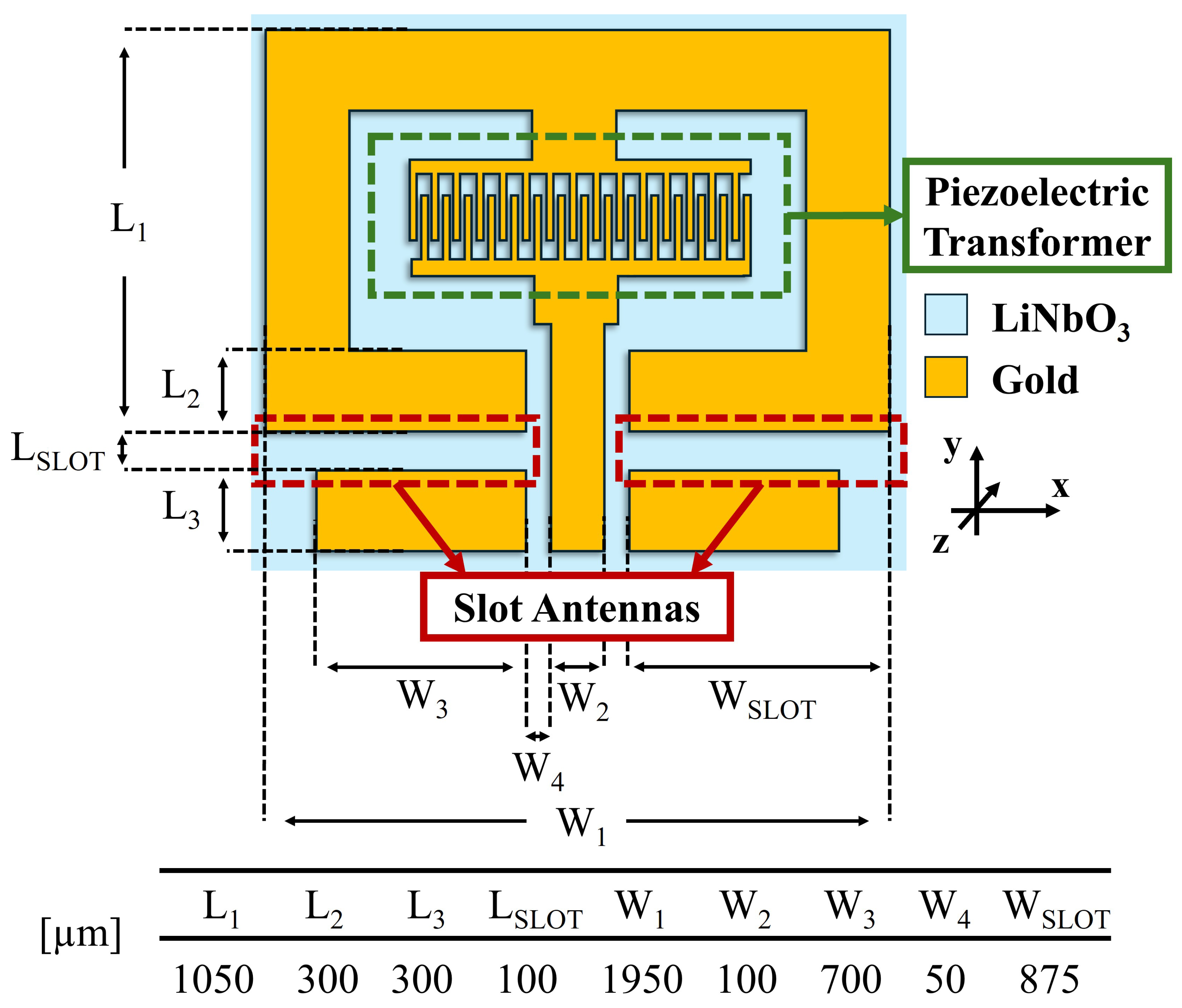
Figure 2.
Finite-element simulated distribution of the component of the electric field when the piezoelectric transformer is replaced by an ideal short and a unit voltage is applied between the signal and ground pads. The two slots exhibit -directed field components of equal magnitude and opposite sign; because of that, these contributions cancel and can be neglected when analyzing the overall radiated power and . The effective slot field in Eq. (2) is taken as the spatial average of the simulated field magnitude over the slot aperture, and is measured at V/m.
Figure 2.
Finite-element simulated distribution of the component of the electric field when the piezoelectric transformer is replaced by an ideal short and a unit voltage is applied between the signal and ground pads. The two slots exhibit -directed field components of equal magnitude and opposite sign; because of that, these contributions cancel and can be neglected when analyzing the overall radiated power and . The effective slot field in Eq. (2) is taken as the spatial average of the simulated field magnitude over the slot aperture, and is measured at V/m.
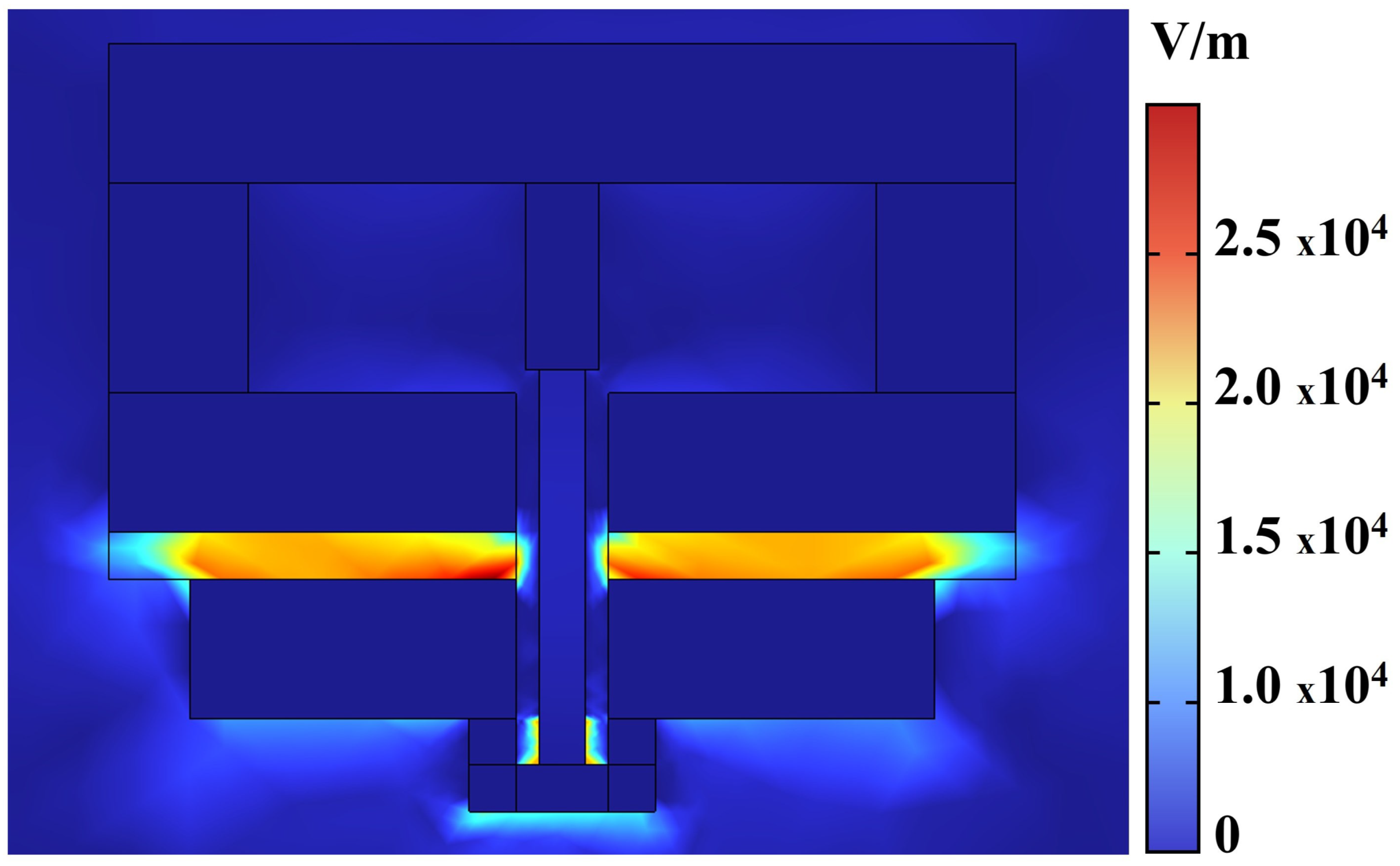
Figure 3.
Simulated trends of vs. for a fixed of 875m. Above a certain value of , saturates and becomes largely independent of further increases in .
Figure 3.
Simulated trends of vs. for a fixed of 875m. Above a certain value of , saturates and becomes largely independent of further increases in .
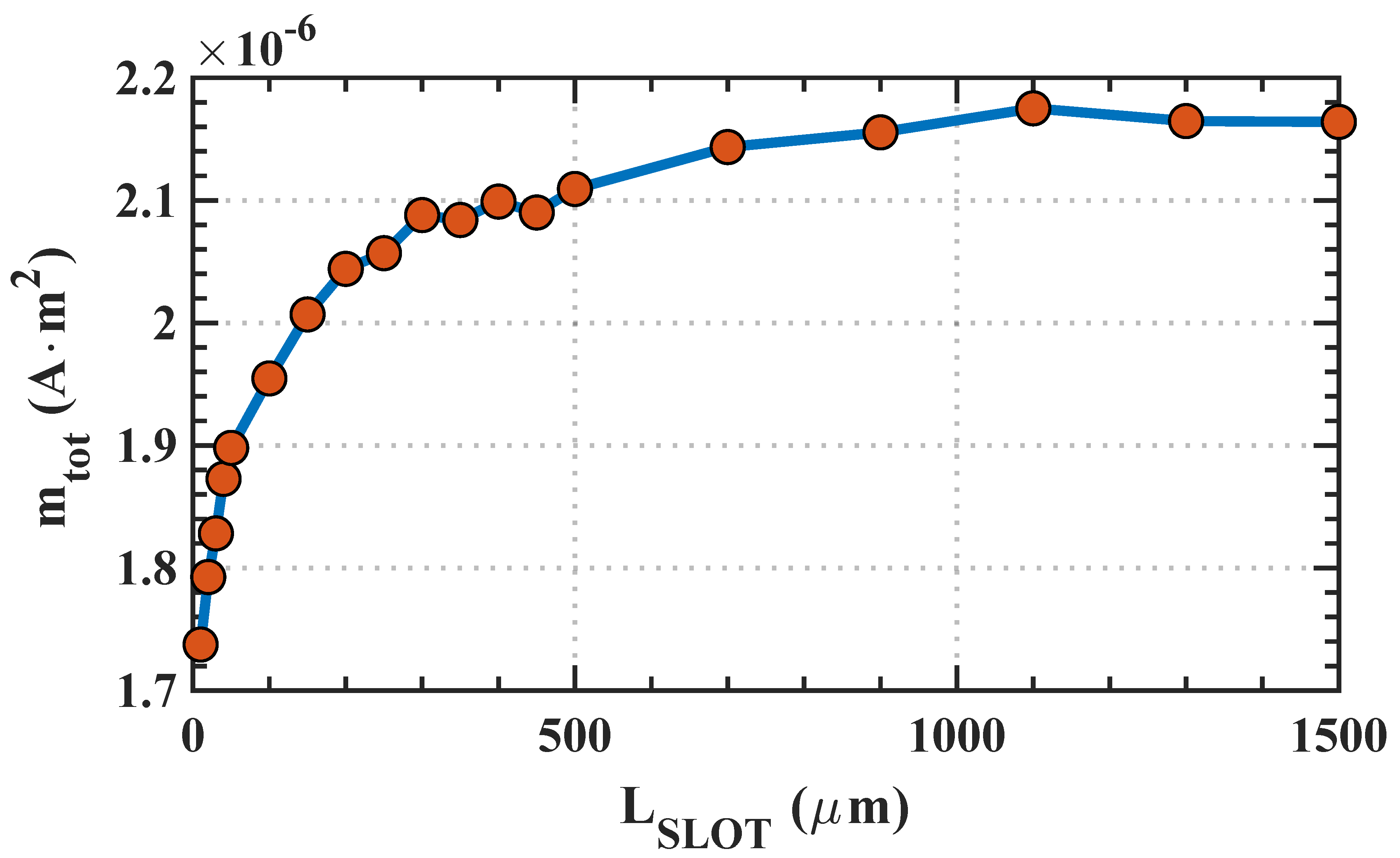
Figure 4.
Simulated trends of vs. for a fixed of 100m. It is evident that grows almost linearly with .
Figure 4.
Simulated trends of vs. for a fixed of 100m. It is evident that grows almost linearly with .
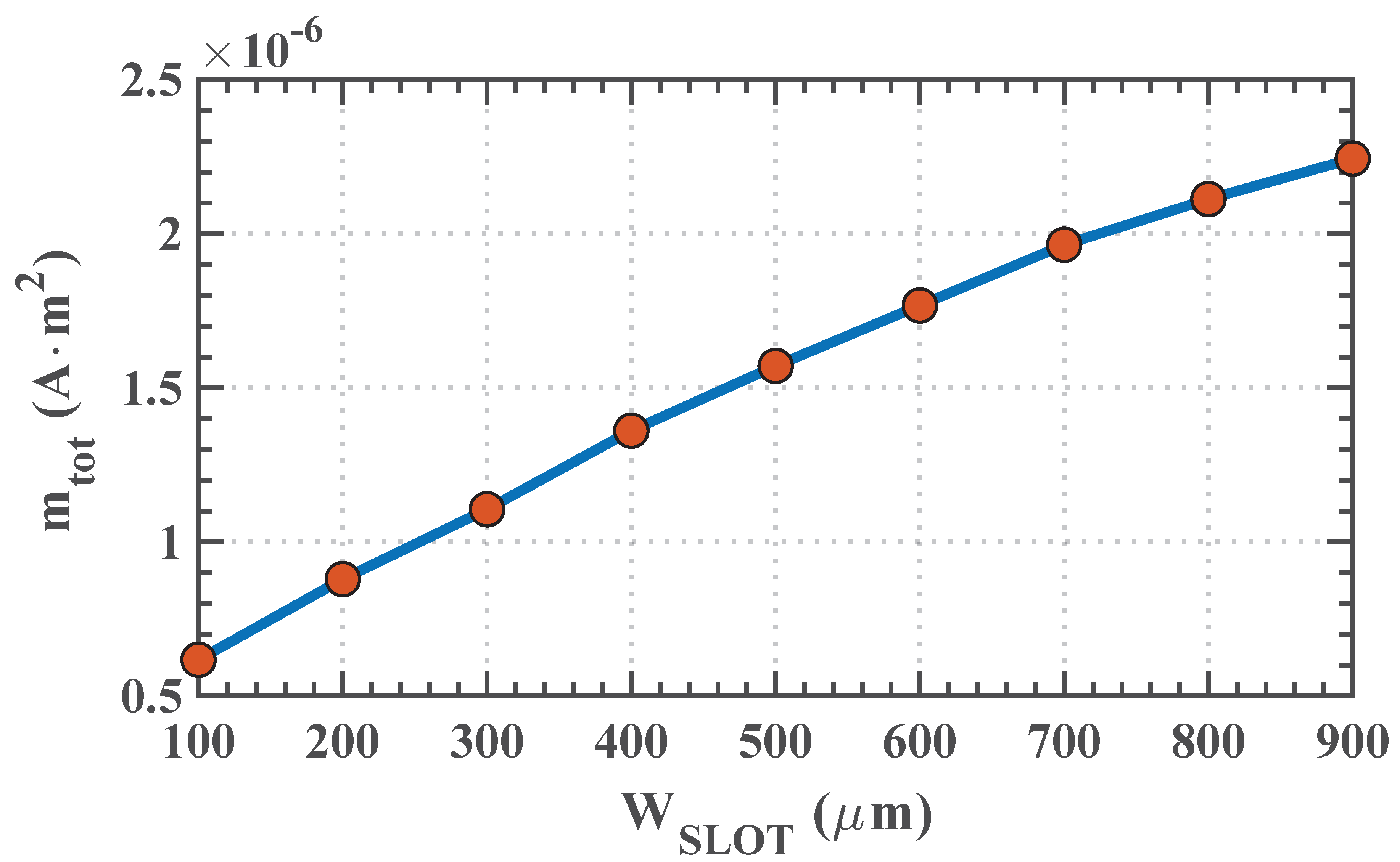
Figure 5.
Circuit schematic of the reported TRX-ESA system, where the LSAW device is modeled using its BVD model and the two slots are modeled by a capacitor, . It is worth emphasizing that the radiation conductance of the slot array is here neglected, since its contribution on and is expected to be negligible (because of the slot’s in-plane dimensions being electrically small).
Figure 5.
Circuit schematic of the reported TRX-ESA system, where the LSAW device is modeled using its BVD model and the two slots are modeled by a capacitor, . It is worth emphasizing that the radiation conductance of the slot array is here neglected, since its contribution on and is expected to be negligible (because of the slot’s in-plane dimensions being electrically small).
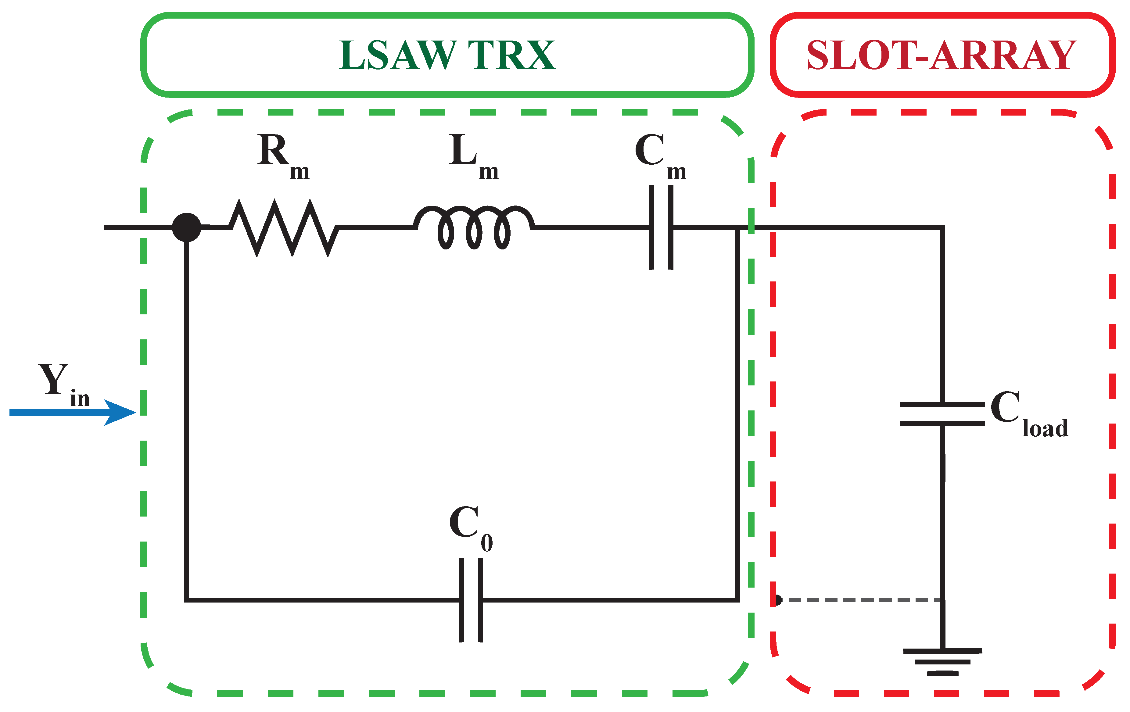
Figure 6.
Simulated trends of vs. the transformer’s and mechanical resonance frequency (i.e., =) when considering a target frequency () for the maximum gain of 425 MHz, as well as a quality factor (Q = 260) and electromechanical coupling coefficient ( = 35%) matching the ones we extracted for the LSAW TRX used in our experimental validation.
Figure 6.
Simulated trends of vs. the transformer’s and mechanical resonance frequency (i.e., =) when considering a target frequency () for the maximum gain of 425 MHz, as well as a quality factor (Q = 260) and electromechanical coupling coefficient ( = 35%) matching the ones we extracted for the LSAW TRX used in our experimental validation.
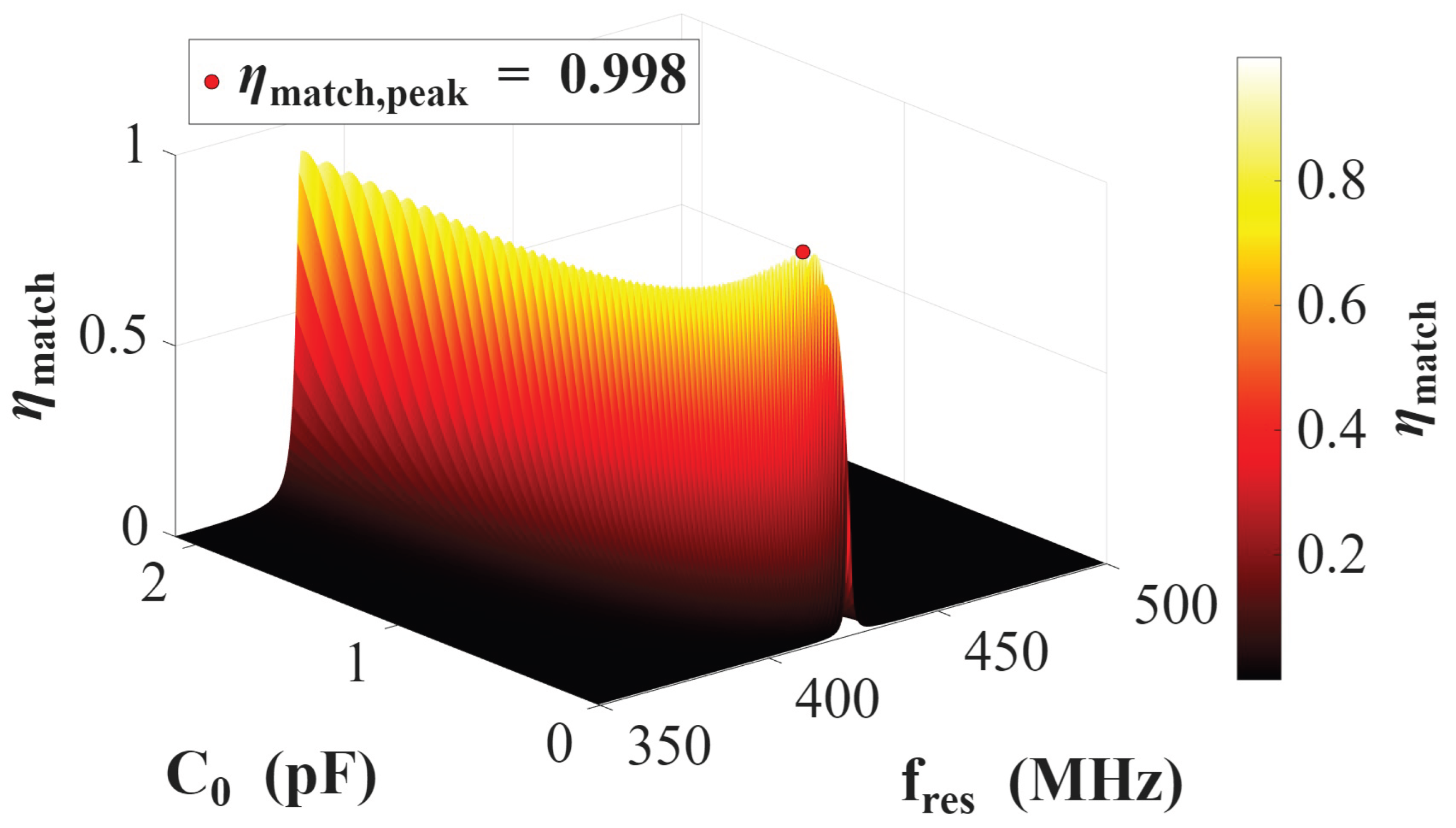
Figure 7.
Two-port network used to derive the voltage gain (). The transformer is represented through a BVD model, with the motional branch in parallel with the static capacitance .
Figure 7.
Two-port network used to derive the voltage gain (). The transformer is represented through a BVD model, with the motional branch in parallel with the static capacitance .
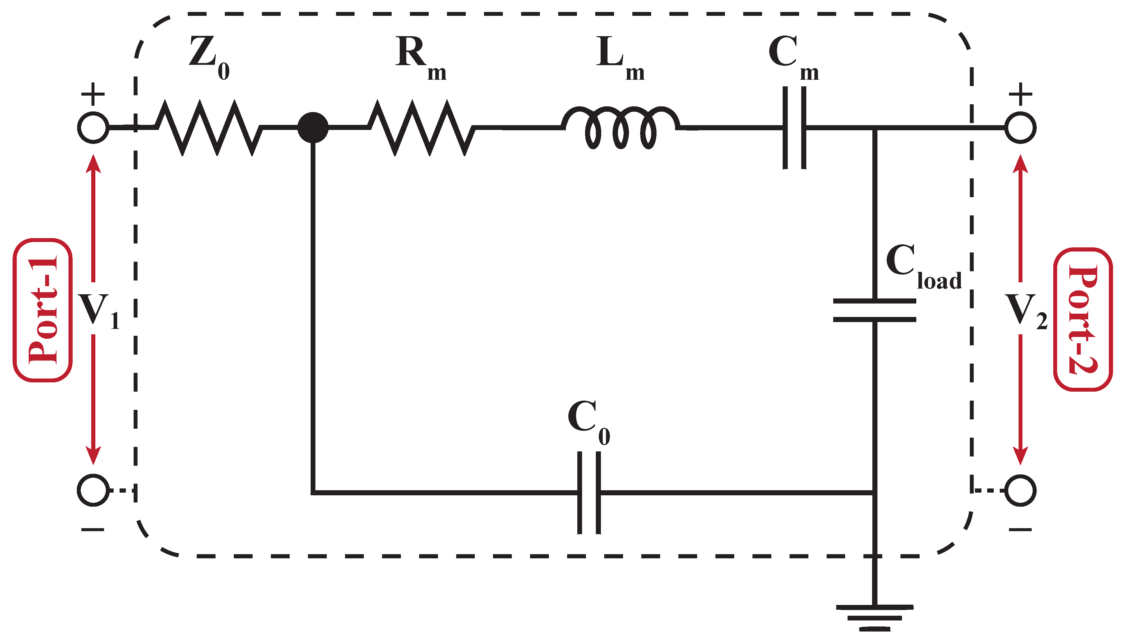
Figure 8.
Simulated trends of vs. the transformer’s and mechanical resonance frequency (i.e., =) when considering a of 425 MHz for the maximum gain, as well as a Q=260 and =35%, matching the ones we extracted for the LSAW TRX we used in our experimental validation.
Figure 8.
Simulated trends of vs. the transformer’s and mechanical resonance frequency (i.e., =) when considering a of 425 MHz for the maximum gain, as well as a Q=260 and =35%, matching the ones we extracted for the LSAW TRX we used in our experimental validation.
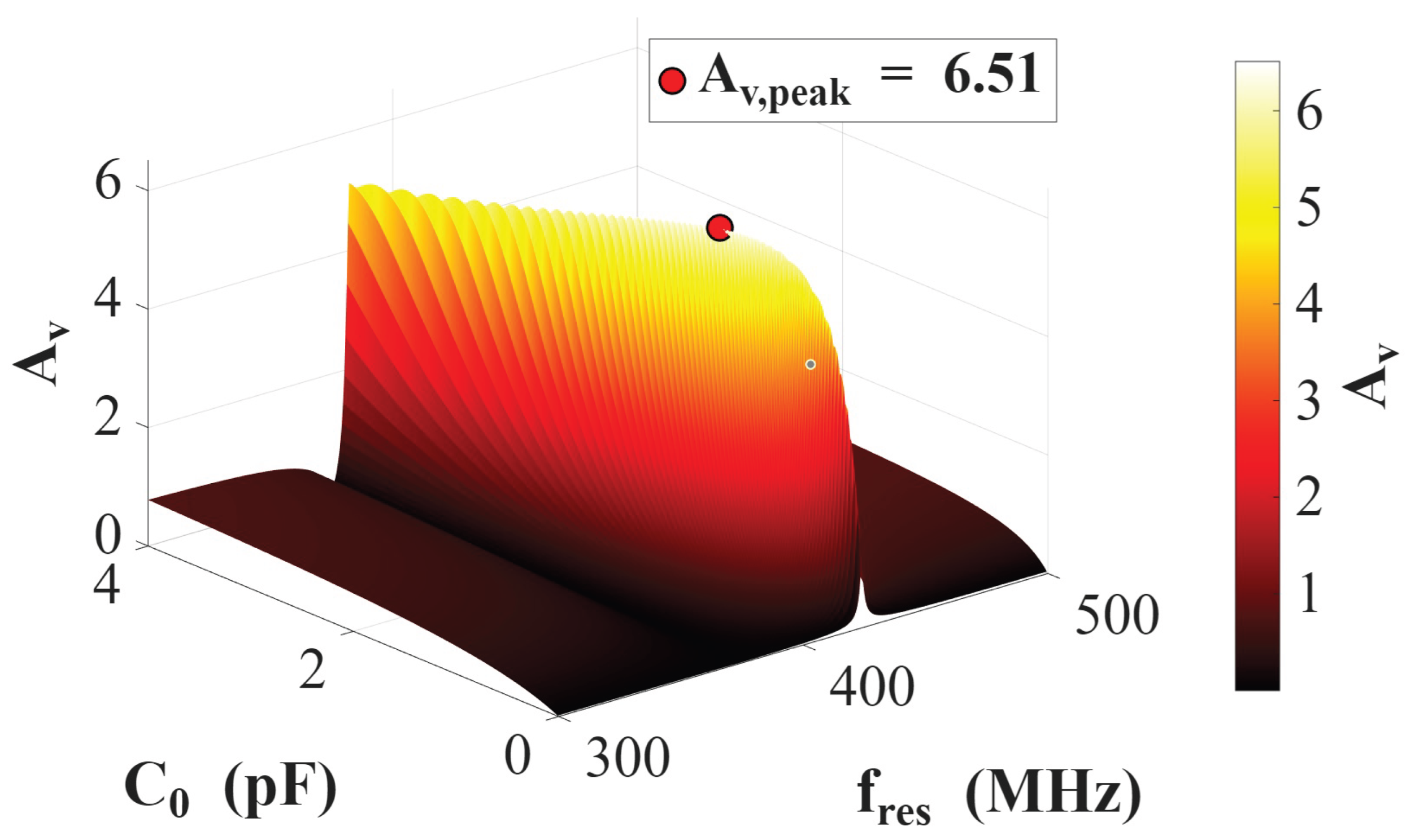
Figure 9.
Simulated trends of vs. the transformer’s and mechanical resonance frequency (i.e., =) when considering a of 425 MHz for the maximum gain, as well as a Q=260 and =35%, matching the ones we extracted for the LSAW TRX we used in our experimental validation.
Figure 9.
Simulated trends of vs. the transformer’s and mechanical resonance frequency (i.e., =) when considering a of 425 MHz for the maximum gain, as well as a Q=260 and =35%, matching the ones we extracted for the LSAW TRX we used in our experimental validation.
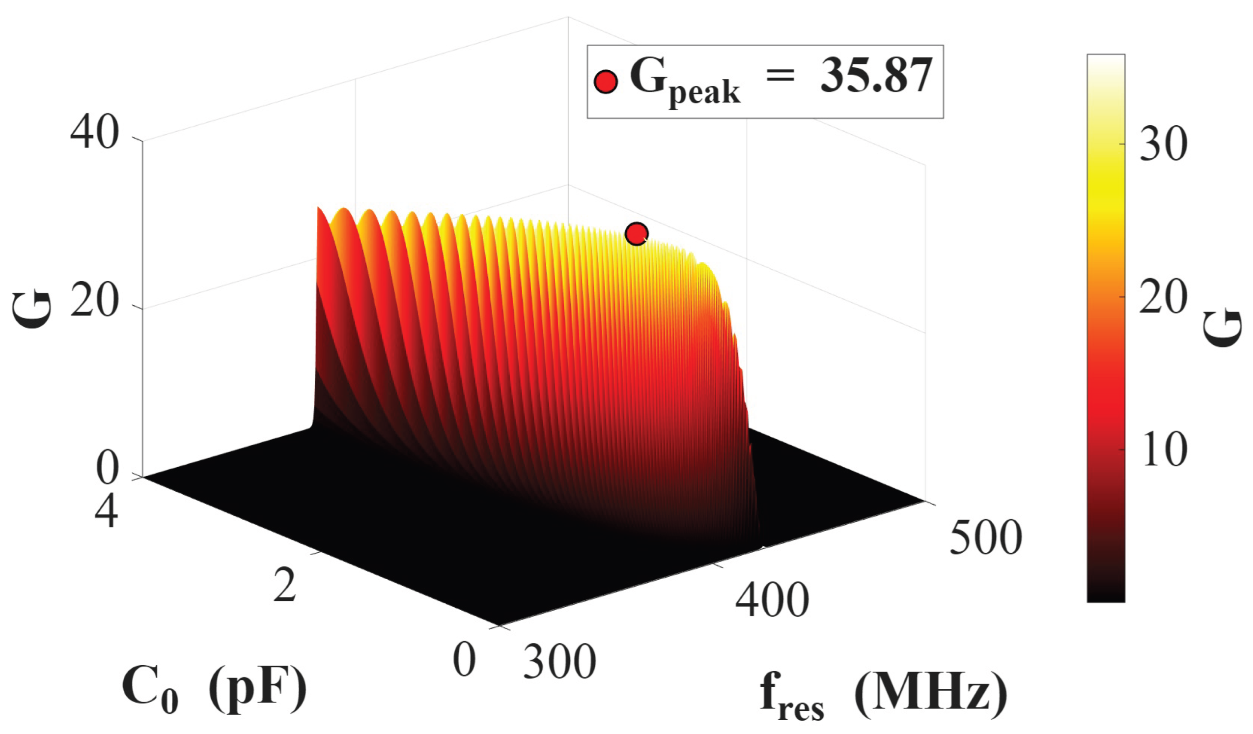
Figure 10.
Simulated and based on the dimensions of the slot array built in this work and on the BVD parameters of the LSAW TRX. is roughly constant within the considered frequency range and approximately equal to -32 dB (see Section II), while shows a peak at of the TRX-ESA system (i.e., at the resonance frequency of ), which differs from due to the stiffening effect of . The maximum gain at is expected to be -15.9 dBi.
Figure 10.
Simulated and based on the dimensions of the slot array built in this work and on the BVD parameters of the LSAW TRX. is roughly constant within the considered frequency range and approximately equal to -32 dB (see Section II), while shows a peak at of the TRX-ESA system (i.e., at the resonance frequency of ), which differs from due to the stiffening effect of . The maximum gain at is expected to be -15.9 dBi.
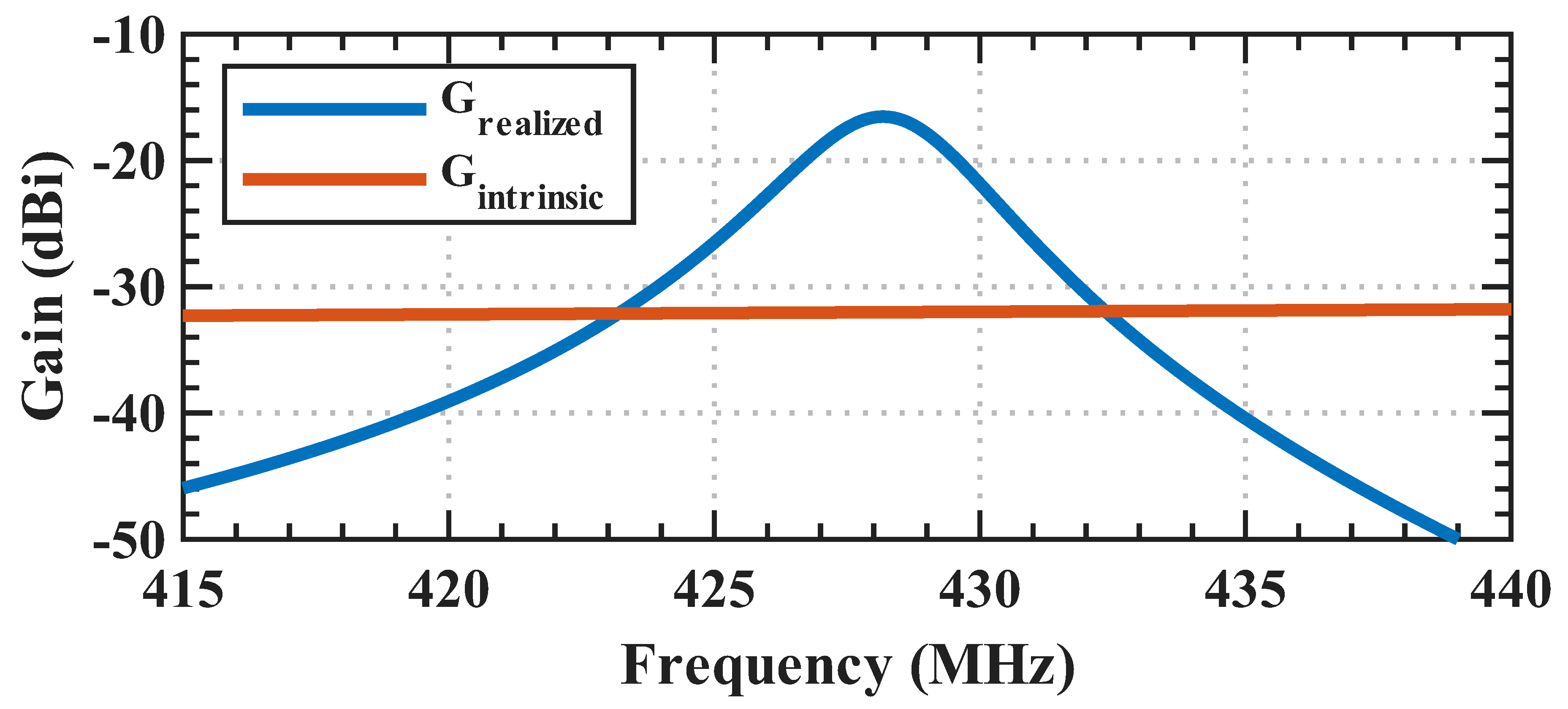
Figure 11.
Investigation of the impact of Q and of on at the experimental of 0.8 pF, showing that increases up to ∼39 with both variables, reaching a plateau for high Q and combinations.
Figure 11.
Investigation of the impact of Q and of on at the experimental of 0.8 pF, showing that increases up to ∼39 with both variables, reaching a plateau for high Q and combinations.
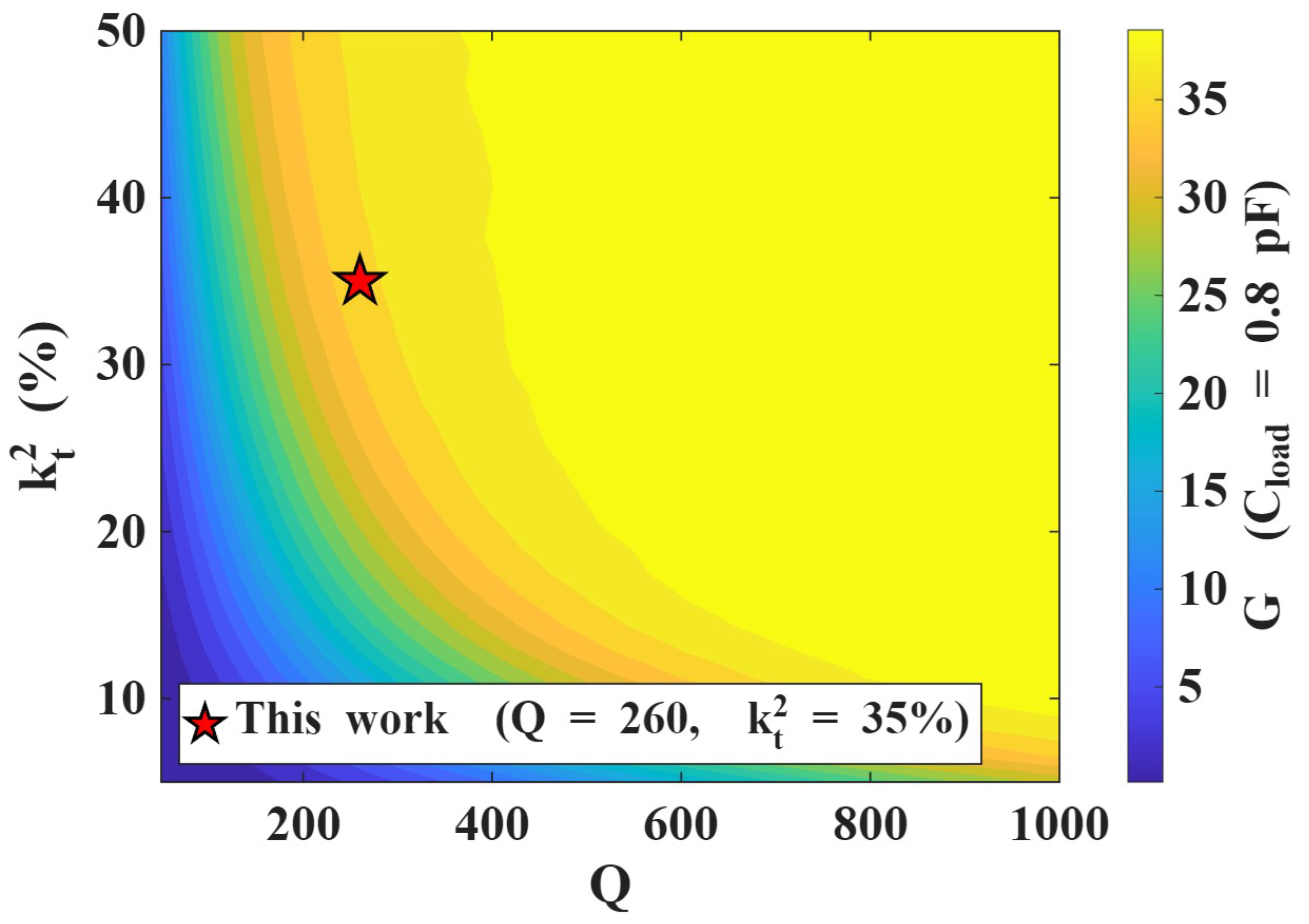
Figure 12.
Investigation of the impact of Q and of on assuming a of 0.2 pF, showing that can sensibly increase when using values for which .
Figure 12.
Investigation of the impact of Q and of on assuming a of 0.2 pF, showing that can sensibly increase when using values for which .
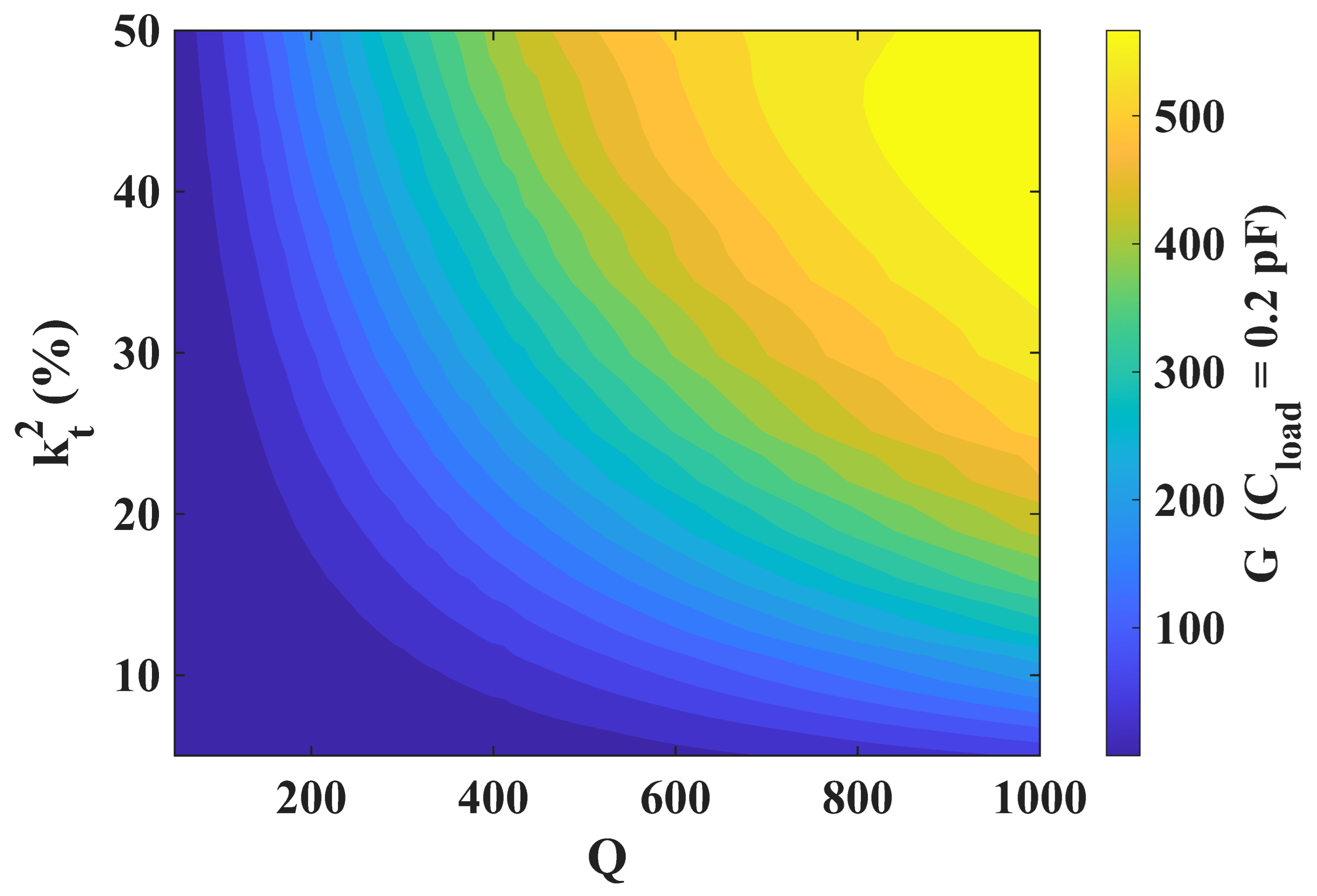
Figure 13.
(a) Illustration of the simulated displacement for the shear horizontal () mode excited in the LSAW device. (b) Simulated as function of . It is evident that the can be maximized when working at ratios close to 0.0375.
Figure 13.
(a) Illustration of the simulated displacement for the shear horizontal () mode excited in the LSAW device. (b) Simulated as function of . It is evident that the can be maximized when working at ratios close to 0.0375.
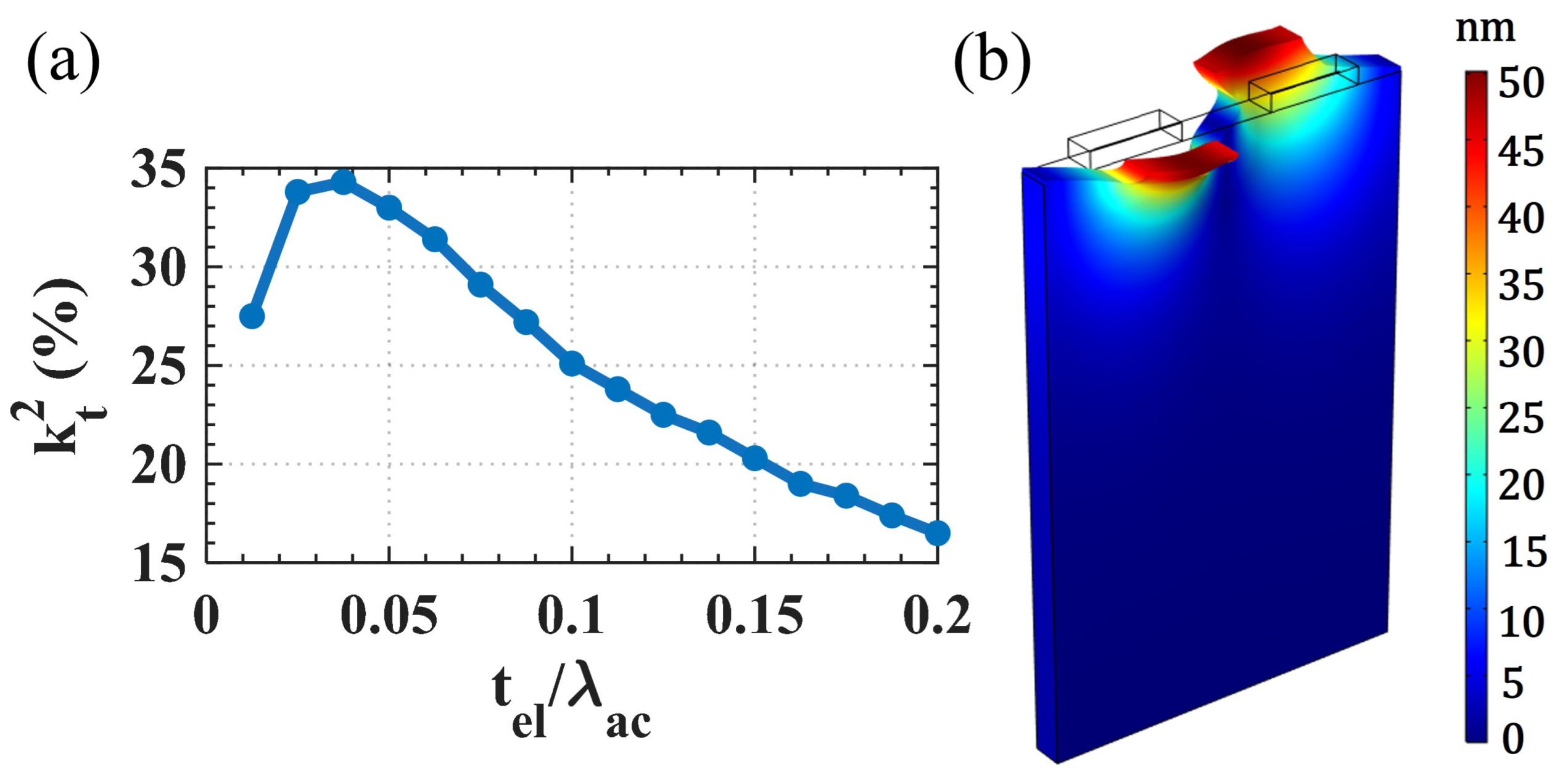
Figure 14.
(a) Fabrication process of the TRX-ESA system. (b) Optical micrograph of the full 2.5 by 2.5 mm chip hosting the fabricated device and (c) scanning electron microscope (SEM) image of the interdigitated transducer (IDT) region.
Figure 14.
(a) Fabrication process of the TRX-ESA system. (b) Optical micrograph of the full 2.5 by 2.5 mm chip hosting the fabricated device and (c) scanning electron microscope (SEM) image of the interdigitated transducer (IDT) region.
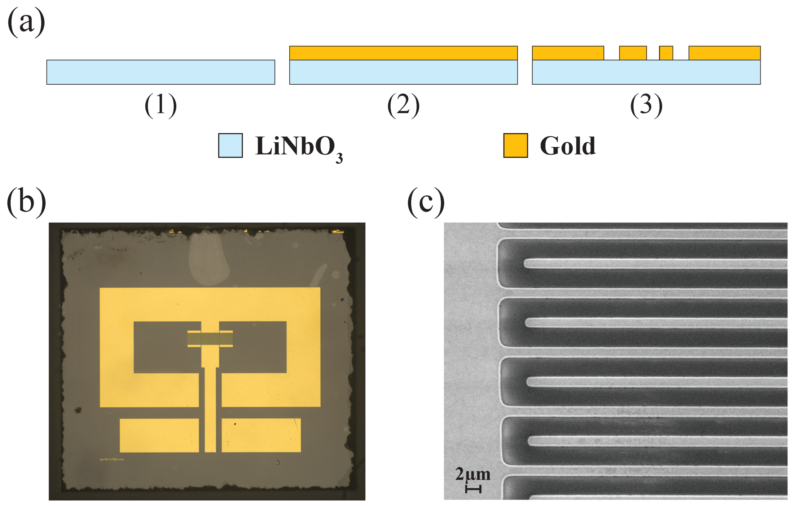
Figure 15.
Experimentally measured response of the TRX-ESA. We also report the two-mode MBVD fitting of the fabricated device, and its relative parameters: =35%, Q=260, =10%, =150, =0.8 pF, =0.27pF, =0.065pF, =0.8 pF, =, =, =, =711.7 nH, =2656 nH, =0.2 pF. A schematic representation of the employed MBVD fitting circuit is reported in the inset.
Figure 15.
Experimentally measured response of the TRX-ESA. We also report the two-mode MBVD fitting of the fabricated device, and its relative parameters: =35%, Q=260, =10%, =150, =0.8 pF, =0.27pF, =0.065pF, =0.8 pF, =, =, =, =711.7 nH, =2656 nH, =0.2 pF. A schematic representation of the employed MBVD fitting circuit is reported in the inset.
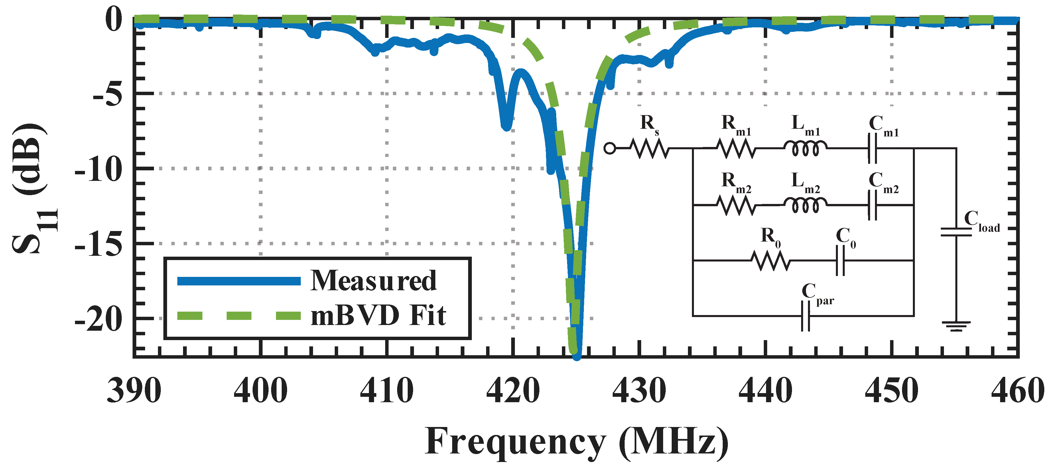
Figure 16.
Illustration and picture of the experimental setup used to extract the realized gain of the TRX-ESA.
Figure 16.
Illustration and picture of the experimental setup used to extract the realized gain of the TRX-ESA.
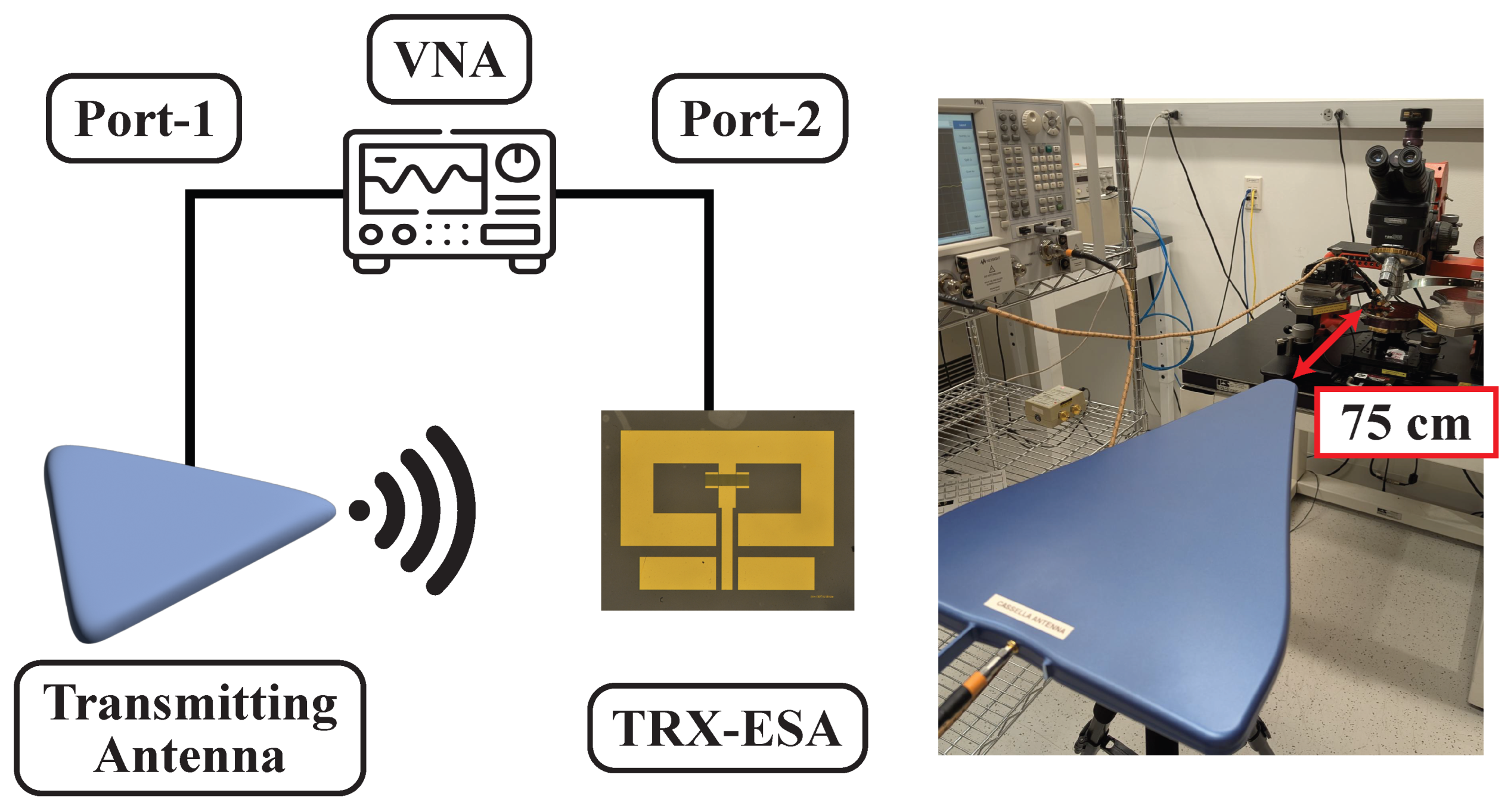
Figure 17.
Experimentally measured realized gain vs. frequency trend of the TRX-ESA. We show a maximum gain of -12.7 dBi, closely matching the value predicted by our analytical model.
Figure 17.
Experimentally measured realized gain vs. frequency trend of the TRX-ESA. We show a maximum gain of -12.7 dBi, closely matching the value predicted by our analytical model.
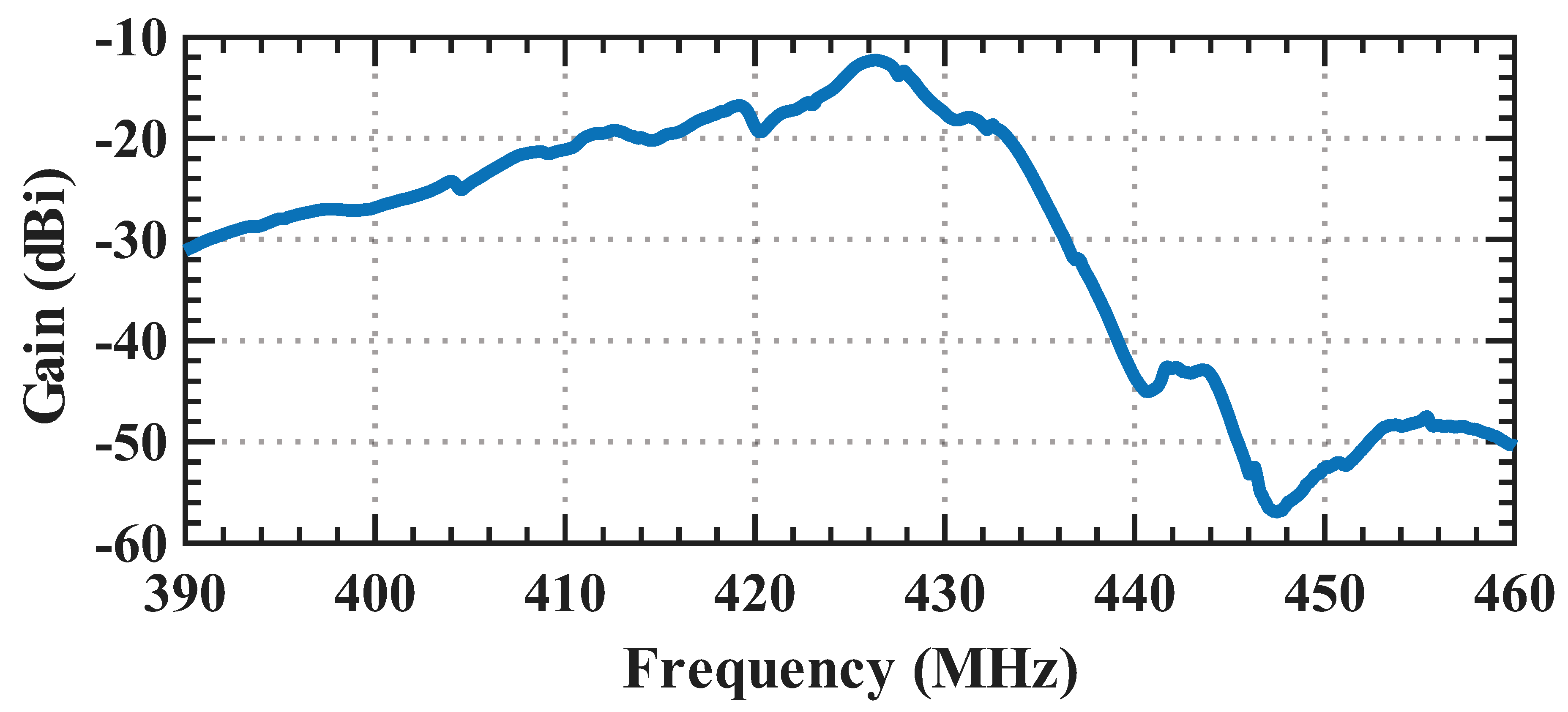

Table 1.
Comparison Between Different On-Chip Antenna Systems
| Work | Type | Material | Frequency (GHz) | Size () | Gain (dBi) | Fractional Bandwidth (-10 dB, %) | GBWP -10 dB () | |
|---|---|---|---|---|---|---|---|---|
| [11] | ME | AlN/FeGaB | 2.55 | 0.7 × 0.8 | - † | -18 | 0.02% # | 0.32 |
| [15] | ME | /FeGaB | 0.43 | 4 × 0.8 ‡ | 8.2% | -28 | 0.93% # | 1.47 |
| [16] | ME | /Ni | 1.87 | 1.88 × 1 | - † | -28.9 | 0% ★ | 0 ★ |
| [41] | ME | /FeGaB | 1.07 | 0.6 × 0.5 | 13.3% | -27.1 | 2.1% | 4.09 |
| [14] | ME | AlScN/FeGaB | 2.62 | 0.7 × 0.8 | 10% | -31.8 | 1.28% | 0.85 |
| [14] | ME | AlScN/FeCoSiB | 3.08 | 0.7 × 0.8 | 10.7% | -29.7 | 1.27% | 1.36 |
| [21] | AMP-ESA | 0.45 | 2.65 × 1.95 | 1.13% | -17.2 | 0% ★ | 0 ★ | |
| This work | TRX-ESA | 0.425 | 1.45 × 1.95 | 35% | -12.7 | 0.53% | 28.5 |
- † k2t and MBVD parameters not provided
- # -10 dB fractional bandwidth estimated from figures and/or from provided MBVD fitting.
- ‡ The dimensions of the feed structure and of the overall device are not provided
- * The return loss is lower than 10 dB, thus not allowing us to quantify the -10 dB fractional bandwidth and therefore the GBWP (%)
Disclaimer/Publisher’s Note: The statements, opinions and data contained in all publications are solely those of the individual author(s) and contributor(s) and not of MDPI and/or the editor(s). MDPI and/or the editor(s) disclaim responsibility for any injury to people or property resulting from any ideas, methods, instructions or products referred to in the content. |
© 2026 by the authors. Licensee MDPI, Basel, Switzerland. This article is an open access article distributed under the terms and conditions of the Creative Commons Attribution (CC BY) license (http://creativecommons.org/licenses/by/4.0/).
Copyright: This open access article is published under a Creative Commons CC BY 4.0 license, which permit the free download, distribution, and reuse, provided that the author and preprint are cited in any reuse.


