
Submitted:
28 May 2026
Posted:
29 May 2026
You are already at the latest version
Abstract
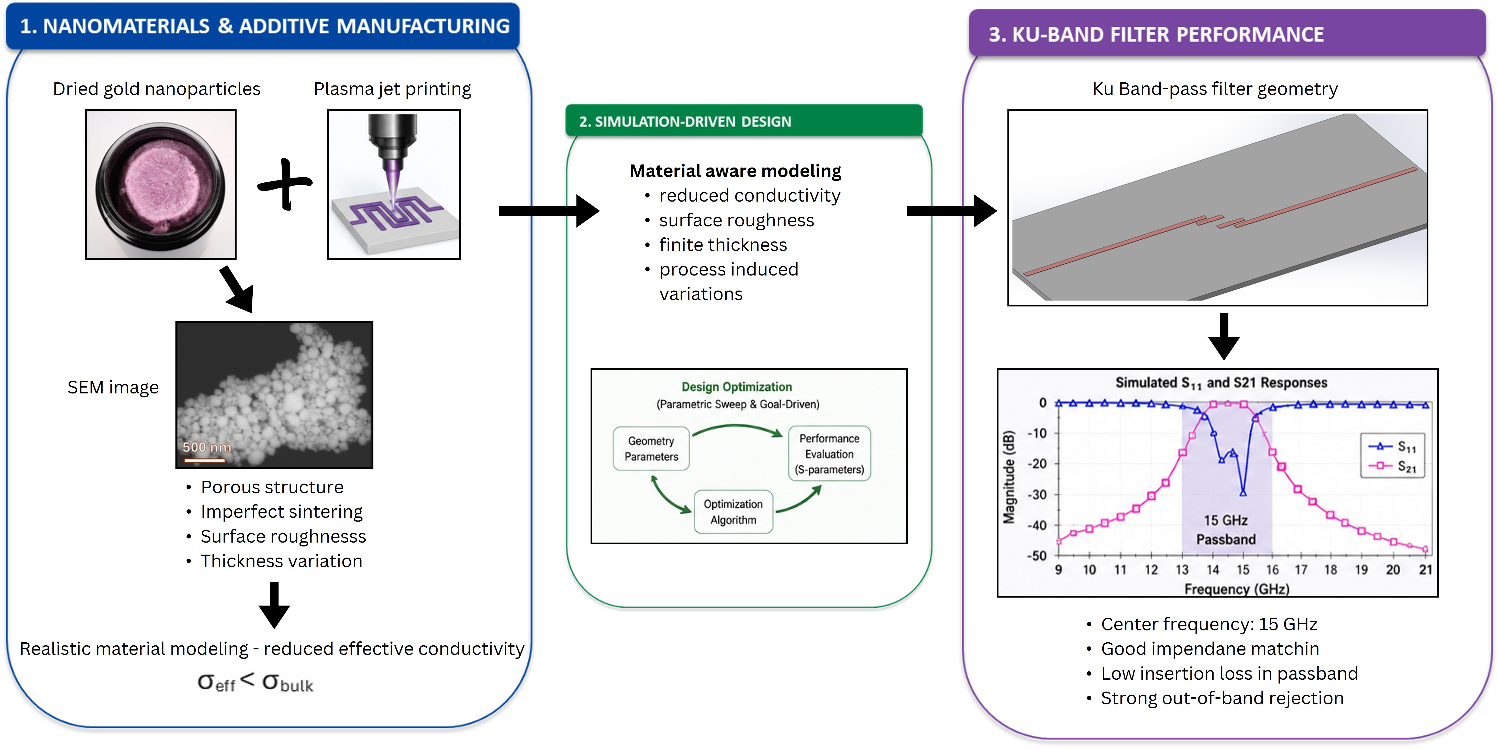
The integration of advanced materials, additive manufacturing processes, and simulation-driven design is becoming increasingly important in the development of high-frequency electronic and machinery components. In this work, a simulation-driven design methodology is presented for gold nanoparticles-based (AuNPs) conductive structures intended for implementation on low-temperature co-fired ceramic (LTCC) substrates. The approach incorporates both electromagnetic performance requirements and manufacturing constraints associated with already developed printed conductive materials. As a representative application, a microstrip coupled-line band-pass filter operating in the Ku-band frequency range is designed using full-wave electromagnetic simulations. The geometry is optimized while considering realistic limitations related to conductor thickness, minimum feature size, and effective electrical conductivity of AuNPs based conductive layers. The AuNPs are produced via ultrasonic spray pyrolysis (USP), liophilizied, dispered in a solvent, plasma printed on a Al2O3 substrate and sintered. The resulting properties thus deviate from bulk gold. The optimized structure of the AuNPs LTCC filter exhibits a center frequency of approximately 15 GHz with a bandwidth of about 1 GHz. Simulated S-parameter results demonstrate efficient signal transmission within the passband and strong attenuation outside the operating frequency range.
Keywords:
gold nanoparticles
; ultrasonic spray pyrolysis
; LTCC substrates
; material modeling
; manufacturing constraints
; high frequency applications
Copyright: This open access article is published under a Creative Commons CC BY 4.0 license, which permit the free download, distribution, and reuse, provided that the author and preprint are cited in any reuse.


