

Submitted:
27 May 2026
Posted:
29 May 2026
You are already at the latest version
Abstract
Recent developments in particle physics require cost-effective pixel detectors capable of operating under increased energy and luminosity conditions foreseen in future collider experiments. In response, monolithic CMOS pixel sensors incorporating modern readout architectures have emerged, combining high-rate capability with substantial radiation tolerance. To optimize the performance of these sensors for application in tracking detectors, a comprehensive characterization has been done focusing on threshold and noise behaviour as a function of front-end DAC tuning parameters. The effect of radiation damage has been investigated using high-intensity X-ray irradiation, followed by a detailed comparison of sensor performance before and after irradiation. The threshold distribution is observed to be uniform across the pixel matrix. Irradiation introduces a systematic shift in the threshold, with a larger impact at low-threshold configurations, while overall uniformity is preserved. In contrast, the noise remains largely stable across the parameter space. The correlation between threshold and noise is used to identify optimal operating regions, demonstrating that stable, efficient performance can be achieved across a wide range of configurations. These results confirm the robustness of the sensor under irradiation and its suitability for operation in radiation environments relevant to future high-energy physics experiments.
Keywords:
particle tracking detectors
; radiation-hard detectors
; electronic detector readout concepts
; CMOS sensors
; monolithic active pixel sensors
; inspection with X-rays
1. Introduction
Current experimental particle physics facilities require efficient tracking detectors that can operate in extremely demanding environments. Experiments at the Large Hadron Collider (LHC) and its future upgrades, such as the High Luminosity LHC (HL-LHC) [1,2], will experience significantly increased particle rates and radiation levels. As a result, detector technologies must provide excellent spatial resolution, fast signal response, and strong radiation tolerance while minimizing the material budget. These requirements have motivated the development of new types of silicon-based pixel detector capable of meeting the performance demands of future collider experiments. One promising technology in this direction is the Depleted Monolithic Active Pixel Sensor (DMAPS) [3,4,5,6,7]. In DMAPS devices, the charge produced during particle passage is collected in a fully or partially depleted silicon region and processed directly by integrated front-end electronics within each pixel. This approach enables faster signal collection through drift mechanisms, improves radiation tolerance, and allows the sensor to be fabricated as a single integrated structure. Furthermore, monolithic sensors can be produced with thinner silicon layers and without custom bump bonding, thereby reducing the material budget and improving overall detector performance. This work discusses recent advances in monolithic active pixel sensors for large-area tracking applications and their performance characteristics. The investigation focuses on the electrical behaviour and the response of the sensor threshold under X-ray irradiation. Understanding these properties is essential for optimizing detector performance and assessing the suitability of their technology for future high-energy physics experiments.
2. The CMOS Monolithic Pixel Sensor
Monolithic pixel detectors play an important role in particle physics experiments because they provide precise spatial information about particle interactions while maintaining high granularity and fast response. As the luminosity and collision rates of experiments such as the Large Hadron Collider increase, detector technologies must be able to operate efficiently at high radiation levels and high hit rates. In this context, CMOS-based monolithic pixel sensors [3,4,5,6,7] have attracted considerable attention because they combine the sensing element and the readout electronics on a single silicon substrate, enabling compact detector designs with a reduced material budget and improved scalability for large detector areas.
The monolithic active pixel sensor [8,9] is developed using a modified TowerJazz 180 nm CMOS technology. The device was developed to satisfy the demands expected in upcoming high-luminosity accelerator facilities, with emphasis on radiation-hard detectors capable of operating under intense particle fluxes. This sensor consists of an active area containing a pixel-matrix, where each pixel has a pitch of approximately . This fine pixel size enables precise particle tracking while maintaining high hit-detection efficiency. The sensor is capable of operating at hit rates approaching , making it suitable for the demanding environment expected in upgraded collider detectors.
The second generation of this monolithic sensor [10,11] is also built in the TowerJazz 180 nm process. It features a pixel matrix over a area, keeping the pixel size the same at . In this second-generation sensor, a shift register replaced the Ethernet-like slow control and an open-loop front-end was used for lower noise and compactness, with gain-enhancing multi-cascode transistors [12,13,14]. Its asynchronous read-out uses a 37-bit data bus and a 4322-bit control register, with read-out handled by a Kintex-7 FPGA on a KC705 board.
2.1. Description of DACs
3. The CMOS Monolithic Pixel Sensor Setup
3.1. Electrical Characterization Setup
The electrical characterization of the second-generation CMOS monolithic pixel sensor was performed using a dedicated readout system. The setup is designed to enable precise threshold and noise measurements through controlled Digital-to-Analog Converter (DAC) scans and stable biasing conditions. The second-generation CMOS monolithic pixel sensor was wired to a custom-designed carrier board at CERN, which provides the required biasing and signal routing. The board distributes multiple independent voltage domains, including the low-voltage digital supply (LVDD), the digital core supply (DVDD), the analog supply (AVDD), and substrate-related biases such as PWELL and SUB. These voltages are critical for the operation of the front-end electronics and for tuning the sensor’s depletion and charge-collection properties. A reference voltage (DREF) is also supplied to the on-chip level shifter circuitry to ensure proper signal reset and logic-level compatibility.
The carrier board interfaces with an FPGA-based evaluation board via a high-speed FMC (FPGA Mezzanine Card) connector. The FPGA platform is responsible for sensor configuration, control, and data acquisition. Communication between the FPGA board and the host computer is established via a standard Ethernet interface, enabling remote operation and data transfer within a local network. Five independent low-voltage power supplies power the system, ensuring stable, noise-minimized operation across the different voltage domains. A high-precision digital multimeter is used to monitor and calibrate the supplied voltages and currents. Care is taken to minimize electrical noise by properly grounding and shielding the setup. Data acquisition and control are handled by the MALTA software framework, implemented in C++ and Python. The software allows for full configuration of the chip registers, execution of DAC scans, and readout of pixel responses. Threshold characterization is performed by scanning the injected charge or equivalent DAC settings and recording the pixel response at each setting. The resulting S-curves are analyzed to extract the effective threshold and noise for each pixel, which are then used in the calculation of the threshold and noise for full pixel sensors and groups.
All measurements are carried out under stable environmental conditions, with the temperature maintained at . Temperature stability is ensured to minimize variations in electronic noise and threshold dispersion. The system allows reproducible measurements across different sensor samples and operating conditions.
3.2. X-Ray Irradiation Setup
CMOS monolithic pixel sensor irradiation studies were carried out using a PRECISION X-Rad160 X-ray irradiator installed in the IIT Madras High Energy Physics Laboratory, as shown in Figure 2(b). The irradiation setup is equipped with a tungsten target and can generate X-rays with tube voltages up to 160 kV, producing a broad bremsstrahlung spectrum suitable for radiation-hardness studies of semiconductor devices.
The sensor under test was placed inside the irradiation chamber at a fixed source-to-specimen distance (SSD) of 30 cm. This configuration was chosen to ensure uniform irradiation across the sensor’s active area. The device alignment within the irradiation field was carefully controlled to minimize spatial dose variations. The dose rate was calibrated to approximately 12.7 Gy/min based on the operating parameters of the X-ray tube, including the applied high voltage (up to 160 kV), the tube current (up to 18.7 mA) and the exposure time. The irradiation was performed using the Time Program mode of the X-Rad160 system, in which X-ray generation is maintained at fixed voltage and current settings and automatically terminated after a predefined exposure duration. In the present study, an exposure time of approximately 13 hours was used to achieve the total ionizing dose.
The delivered dose was determined from the calibrated dose rate and exposure time. Systematic uncertainties in dose estimation arise from irradiator calibration and possible variations in beam uniformity, and these are taken into account in the analysis. During irradiation, the sensor was kept under controlled conditions inside the chamber. The bias configuration during irradiation was maintained to be consistent with the measurement requirements, ensuring reproducibility of the radiation effects. After irradiation, the sensor was removed and subjected to electrical characterization under the same controlled temperature conditions as prior to irradiation. The time interval between irradiation and subsequent measurements was minimized to reduce the impact of annealing effects. All post-irradiation measurements were performed at a controlled temperature of , consistent with the pre-irradiation characterization, allowing a direct comparison of sensor performance before and after exposure.
3.3. Measurement Strategy
To evaluate the impact of irradiation on sensor performance, a comparative analysis was performed using DAC-based threshold scans across sensors of different thicknesses. Measurements were carried out both before and after irradiation under identical operating conditions using a setup at IIT Madras, as shown in Figure 2(a). The threshold and noise distributions were extracted from the S-curve fits, enabling a systematic study of radiation-induced variations. The use of a consistent electrical setup, controlled environmental conditions, and calibrated irradiation parameters ensures the reliability and reproducibility of the results presented in this work.
4. Irradiation Results and Discussion
4.1. Threshold Behaviour
The sensor’s threshold distribution is first evaluated at a representative operating point corresponding to the DAC configuration , , and . The threshold is extracted from the S-curve of individual pixels, obtained from the response as a function of the injected charge, as illustrated for a representative pixel in Figure 3(a).
Figure 3(c) shows the resulting two-dimensional threshold map of the pixel matrix. The distribution is observed to be largely uniform across the matrix, with only mild spatial variations. No significant localized structures or defective regions are visible, indicating good pixel-to-pixel uniformity at this operating point. The corresponding one-dimensional distribution of the threshold values is shown in Figure 3(b). The distribution is well described by a Gaussian with a mean threshold of approximately and a standard deviation of approximately . The relatively narrow spread demonstrates good intrinsic threshold uniformity of the sensor, which is essential for stable operation and uniform detection efficiency across the pixel matrix.
4.1.1. Dependence of Threshold on DAC Parameters and Irradiation
The dependence of the threshold on the front-end tuning parameters is studied by varying , , and . Figure 4 illustrates the dependence of the mean threshold on , where each point corresponds to the average over all available configurations of and .
A decreasing trend of threshold with increasing is observed for both unirradiated and irradiated data. The irradiated sensor consistently exhibits lower threshold values compared to the unirradiated case across the full range of . The distribution spreads, represented by the error bars, remain comparable, indicating that irradiation does not significantly degrade threshold uniformity. To further investigate the combined dependence on and , two-dimensional threshold maps are constructed for a fixed value of , as shown in Figure 5. A clear monotonic increase of threshold with increasing is observed, while a weaker dependence on is seen. A comparison between unirradiated and irradiated conditions reveals a systematic shift in threshold across the parameter space. The absolute change in threshold, shown in Figure 5 (bottom left), indicates an increase of up to – for low values. The effect is more pronounced at lower threshold settings, suggesting increased sensitivity of these configurations to irradiation. The relative variation, shown in Figure 5 (bottom right), remains below over most of the parameter space, with the largest deviations occurring at low . At higher values, the relative change is significantly reduced, indicating a more stable operating regime under irradiation. These results demonstrate that, while irradiation introduces a measurable shift in the threshold, a wide range of parameter configurations remains operational, allowing optimization of detector performance by selecting appropriate DAC settings.
The dependence of the sensor threshold on is shown in Figure 6, with the mean threshold presented versus for both unirradiated and irradiated data. A relatively weak dependence on is observed compared to other tuning parameters. The threshold varies only mildly across the scanned range, indicating that plays a secondary role in threshold tuning. The two-dimensional threshold maps for a fixed value of are shown in Figure 7, where the variation with and is explored. A clear gradient is observed along the axis, while the dependence on remains moderate, consistent with the trends discussed earlier. After irradiation, a systematic shift in the sensor threshold is observed across all values. The absolute change in threshold is larger at lower values, as seen in Figure 7 (bottom plots), while the relative variation remains below over most of the parameter space. This indicates that does not significantly affect the radiation-induced degradation, and the sensor response remains stable with respect to this parameter.
The dependence of the sensor threshold on is shown in Figure 8. A strong, nearly linear increase in the threshold with increasing is observed in both unirradiated and irradiated data. This demonstrates that is the primary parameter controlling the sensor’s absolute threshold. The separation between the unirradiated and irradiated curves remains approximately constant across the full range of , indicating a systematic shift induced by irradiation. The distributions’ spreads are comparable in both cases, suggesting that threshold uniformity is preserved after irradiation. The two-dimensional threshold maps for a fixed value of are shown in Figure 9. The dependence on and is relatively weak compared to the dominant effect of , confirming that this parameter governs the global threshold scale. The absolute threshold shift, shown in Figure 9 (bottom plots), indicates variations up to – depending on the parameter configuration. The relative change remains below in most regions, with slightly larger deviations observed at low values. These results demonstrate that provides a robust handle to tune the threshold while maintaining stability under irradiation, making it the key parameter for optimizing detector performance.
Overall, the threshold behaviour of the monolithic pixel sensor is primarily governed by , which controls the global threshold scale, while provides additional tuning of the front-end response. In contrast, exhibits only a weak influence on the threshold. Irradiation introduces a systematic shift in threshold across all parameter configurations, with a more pronounced effect at lower threshold settings. However, the relative variation remains within acceptable limits over a wide range of operating conditions, indicating that stable operation can be achieved through appropriate tuning of the DAC parameters.
4.2. Noise Performance
The sensor’s noise performance is evaluated using the width of the S-curve for individual pixels, which provides a measure of the equivalent noise charge (ENC). The dependence of noise on the front-end tuning parameters , , and is studied for both unirradiated and irradiated conditions. The Figure 10 shows the 1-dimensional noise distributions of the sensor and 2-dimensional noise distributions over all pixels, respectively.
4.2.1. Dependence of Noise on DAC Parameters
The dependence of noise on is shown in Figure 11(a). The noise remains relatively stable across the scanned range of , with only minor variations of the order of –. This indicates that has a limited impact on the sensor’s intrinsic noise performance. A comparison between unirradiated and irradiated data shows a slight increase in noise after irradiation. However, the overall variation remains small, and no significant degradation of noise performance is observed.
The variation of noise with is shown in Figure 11(b). A weak dependence on is observed, with noise values remaining nearly constant over the full range of the parameter. This confirms that does not significantly affect noise performance. After irradiation, a modest increase in noise is observed; however, the absolute variation remains limited to –, indicating stable behaviour under irradiation. The dependence of noise on is presented in Figure 11(c). A slight increase in noise is observed with increasing , although the effect remains weaker than the corresponding dependence of the threshold. The separation between unirradiated and irradiated data is small across the full range, indicating that irradiation has only a limited impact on the noise performance. The spread of the distributions remains comparable, suggesting that noise uniformity across the pixel matrix is preserved.
Overall, the noise shows only a weak dependence on the tuning parameters and exhibits a modest increase after irradiation. In contrast to threshold, which is strongly affected by parameter tuning, the noise remains stable across a wide range of configurations. This demonstrates that the sensor maintains good noise performance even after radiation exposure.
4.3. Noise vs Threshold Studies
The optimization of the second-generation monolithic pixel sensor operating point is performed by studying the correlation between threshold and noise for different configurations of the front-end tuning parameters. This allows identification of regions in the parameter space that provide an optimal balance between low threshold and acceptable noise performance.
Figure 12(a) shows the correlation between threshold and noise with respect to , while keeping and constant. Each point corresponds to a different setting. A clear horizontal trend is observed, with the threshold varying significantly, while the noise remains nearly constant. This indicates that can be used to fine-tune the threshold without introducing a substantial noise penalty. A comparison between unirradiated and irradiated data shows a consistent shift towards lower threshold values after irradiation, while the noise increases only slightly. The overall structure of the correlation remains unchanged, demonstrating that the tuning behaviour is preserved under irradiation. The dependence on is shown in Figure 12(c), where a strong correlation between threshold and noise is observed. As increases, the threshold shifts upward significantly while the noise increases only mildly. This confirms that is the primary parameter controlling the sensor’s operating point, enabling a wide range of threshold values to be accessed. In contrast, Figure 12(b) shows the dependence on , where only a weak variation in both threshold and noise is observed. The data points cluster in a narrow region, indicating that has a limited impact on the overall performance and mainly serves as a secondary tuning parameter.
The combined results demonstrate that the optimal operating region corresponds to configurations with moderate values, where the threshold is sufficiently low while maintaining stable noise performance. Extremely low-threshold configurations, although achievable, tend to be more sensitive to irradiation effects and exhibit larger relative variations. Overall, the sensor provides a flexible tuning space, with defining the global threshold scale, enabling fine adjustment, and ensuring stable operation. Preservation of the threshold–noise correlation after irradiation confirms the sensor’s robustness and suitability for operation in radiation environments. These results demonstrate that the detector can be operated in a regime that simultaneously ensures low threshold, controlled noise, and stability under irradiation, fulfilling the requirements for high-efficiency tracking applications.
4.4. Radiation-Induced Threshold Shift
To further quantify the impact of irradiation, the average threshold shift is evaluated with respect to the tuning parameters. For every parameter setting, the threshold difference between irradiated and unirradiated data is calculated by averaging over all configurations of the remaining parameters.
The dependence of the threshold shift on is shown in Figure 13(a). A clear decreasing trend is observed with increasing , indicating that configurations with lower threshold settings are more sensitive to radiation effects. The largest shifts are observed at low , while higher values provide a more stable response. The variation with , illustrated in Figure 13(b), exhibits a behaviour that is not monotonic, reaching a maximum near intermediate values. This suggests that the radiation response is influenced by the front-end shaping conditions, with certain configurations being more susceptible to irradiation-induced changes. In contrast, the dependence on , shown in Figure 13(c), is relatively weak. Only small variations in the threshold shift are observed in the full range of , indicating that this parameter has a limited impact on radiation sensitivity.
Overall, these results demonstrate that the radiation-induced threshold shift is primarily driven by , while introduces secondary effects and plays a minimal role. This reinforces the conclusion that stable operation under irradiation can be achieved by selecting appropriate values, avoiding configurations with excessively low thresholds.
5. Conclusions
The performance of the second-generation CMOS monolithic pixel sensor has been systematically studied with respect to threshold and noise behaviour, with particular emphasis on the dependence on front-end tuning DAC parameters and the impact of irradiation. The threshold distribution is found to be uniform across the pixel matrix, with a narrow spread of approximately at representative operating conditions. A detailed scan of the tuning parameters shows that is the dominant parameter controlling the absolute threshold, with a strong, nearly linear dependence. The parameter provides additional fine-tuning of the threshold, while has only a minor influence. Irradiation results in a systematic shift in the threshold across the parameter space. Interestingly, the threshold decreases after irradiation, while the overall threshold uniformity is preserved. A dedicated study of radiation-induced threshold shift demonstrates that configurations with lower threshold settings are more sensitive to radiation effects, with the largest variations observed at low . In contrast, higher values provide a more stable response under irradiation. The dependence on is non-monotonic, while has a minimal impact on radiation sensitivity.
The sensor’s noise performance is observed to be stable across all tuning parameters, with only a weak dependence on , , and . After irradiation, a modest increase in noise is observed; however, the overall variation remains small, and the noise uniformity across the matrix is preserved. The combined analysis of threshold and noise demonstrates that the pixel sensor offers a flexible tuning space, allowing optimization of the operating point. The threshold-noise correlation remains well-defined both before and after irradiation, enabling selection of configurations that achieve low thresholds while maintaining acceptable noise levels. Overall, these results confirm the sensor’s robustness under irradiation and demonstrate that stable, efficient operation can be achieved through appropriate tuning of the front-end parameters. This makes the sensor a promising candidate for use in radiation environments requiring precise tracking performance.
Author Contributions
Conceptualization, M.M.A., G.D. and P.K.B.; methodology, M.M.A. and G.D.; validation, M.M.A. and G.D.; formal analysis, M.M.A. and G.D.; visualization, M.M.A and G.D.; investigation, M.M.A., G.D., A.V. and T.C.; Setup, G.D. and A.V. ; Data Collection, M.M.A., G.D., A.V. and T.C.; resources, P.K.B.; data curation, M.M.A. and G.D.; writing—original draft preparation, M.M.A. and G.D.; writing—review and editing, M.M.A., G.D. and P.K.B.; supervision, P.K.B.; project administration, P.K.B.; funding acquisition, P.K.B. All authors have read and agreed to the published version of the manuscript.
Funding
The project has been funded by the Science and Engineering Research Board (SERB), India grant number PHY1819374SERBPRAF, and the Ministry of Human Resource Development (MHRD), India under grant number SB22231258PHETWO008356.
Data Availability Statement
The datasets generated and/or analyzed during the current study are available from the corresponding authors on reasonable request. Due to the large data volume (terabyte scale), the data are not publicly archived.
DURC Statement
Current research is limited to the High energy Physics, which is beneficial for particle detector development and does not pose a threat to public health or national security. Authors acknowledge the dual-use potential of the research and confirm that all necessary precautions have been taken to prevent potential misuse. As an ethical responsibility, authors strictly adhere to relevant national and international laws about DURC. Authors advocate for responsible deployment, ethical considerations, regulatory compliance, and transparent reporting to mitigate misuse risks and foster beneficial outcomes.
Acknowledgments
We thank to CERN and Experiment Physics group for the support and guidance.
Conflicts of Interest
The authors declare no conflicts of interest. The funders had no role in the design of the study; in the collection, analyses, or interpretation of data; in the writing of the manuscript; or in the decision to publish the results.
References
- High-Luminosity Large Hadron Collider (HL-LHC): Technical Design Report V. 0.1; Apollinari, G., Béjar Alonso, I., Brüning, O., Fessia, P., Lamont, M., Rossi, L., Tavian, L., Eds.; CERN: Geneva, Switzerland, 2017; p. CERN-2017-007-M. [Google Scholar] [CrossRef]
- ATLAS Collaboration. Technical Design Report for the ATLAS Inner Tracker Pixel Detector CERN-LHCC-2017-021, ATLAS-TDR-030; CERN: Geneva, Switzerland, 2017. [Google Scholar] [CrossRef]
- Snoeys, W. CMOS monolithic active pixel sensors for high energy physics. Nucl. Instrum. Methods Phys. Res. Sect. A 2014, 765, 167–171. [Google Scholar] [CrossRef]
- Dingfelder, J.; Barbero, M.; Barrillon, P.; Berdalovic, I.; Bespin, C.; Breugnon, P.; Caicedo, I.; Cardella, R.; Degerli, Y.; Flores Sanz de Acedo, L.; Guilloux, F.; Habib, A.; Hirono, T.; Hemperek, T.; Hügging, F.; Krüger, H.; Kugathasan, T.; Moustakas, K.; Pangaud, P.; Pernegger, H.; Piro, F.; Pohl, D.-L.; Riedler, P.; Rozanov, A.; Rymaszewski, P.; Schwemling, P.; Snoeys, W.; Wang, T.; Wermes, N.; Zhang, S. Progress in DMAPS developments and first tests of the Monopix2 chips in 150 nm LFoundry and 180 nm TowerJazz technology. Nucl. Instrum. Methods Phys. Res. Sect. A 2022, 1034, 166747. [Google Scholar] [CrossRef]
- Darwish, H.; Andary, J.; Arnoldi-Meadows, B.; Artz, O.; Baudot, J.; Bertolone, G.; Besson, A.; Bialas, N.; Bugiel, R.; Claus, G.; Colledani, C.; Deveaux, M.; Dorokhov, A.; Dozière, G.; El Bitar, Z.; Fröhlich, I.; Goffe, M.; Hebermehl, F.; Himmi, A.; Hu-Guo, C.; Jaaskelainen, K.; Keller, O.; Koziel, M.; Matejcek, F.; Michel, J.; Morel, F.; Müntz, C.; Pham, H.; Schmidt, C. J.; Schreiber, S.; Specht, M.; Spicker, D.; Stroth, J.; Valin, I.; Weirich, R.; Zhao, Y.; Winter, M. Tolerance of the MIMOSIS-1 CMOS Monolithic Active Pixel Sensor to ionizing radiation. J. Instrum. 2023, 18, C06013. [Google Scholar] [CrossRef]
- Aglieri Rinella, G. The ALPIDE pixel sensor chip for the upgrade of the ALICE Inner Tracking System. Nucl. Instrum. Methods Phys. Res. Sect. A 2017, 845, 583–587. [Google Scholar] [CrossRef]
- Berdalovic, I.; Bates, R.; Buttar, C.; Cardella, R.; Egidos Plaja, N.; Hemperek, T.; Hiti, B.; van Hoorne, J. W.; Kugathasan, T.; Mandic, I.; Maneuski, D.; Marin Tobon, C. A.; Moustakas, K.; Musa, L.; Pernegger, H.; Riedler, P.; Riegel, C.; Schaefer, D.; Schioppa, E. J.; Sharma, A.; Snoeys, W.; Solans Sanchez, C.; Wang, T.; Wermes, N. Monolithic pixel development in TowerJazz 180 nm CMOS for the outer pixel layers in the ATLAS experiment. J. Instrum. 2018, 13, C01023. [Google Scholar] [CrossRef]
- Pernegger, H. Monolithic pixel development in TowerJazz 180 nm CMOS for the outer pixel layers in the ATLAS experiment. Nucl. Instrum. Methods Phys. Res. Sect. A 2019, 924, 92–98. [Google Scholar] [CrossRef]
- Cardella, R.; Asensi Tortajada, I.; Berdalovic, I.; Bespin, C.; Dachs, F.; Dao, V.; Flores Sanz de Acedo, L.; Piro, F.; Hemperek, T.; Hirono, T.; Hiti, B.; Kugathasan, T.; Marin Tobon, C. A.; Moustakas, K.; Pernegger, H.; Riedler, P.; Schioppa, E. J.; Sharma, A.; Simon Argemi, L.; Snoeys, W.; Solans Sanchez, C.; Wang, T.; Wermes, N. MALTA: an asynchronous readout CMOS monolithic pixel detector for the ATLAS High-Luminosity upgrade. J. Instrum. 2019, 14, C06019. [Google Scholar] [CrossRef]
- Piro, F.; Allport, P.; Asensi, I.; Berdalovic, I.; Bortoletto, D.; Buttar, C.; Cardella, R.; Charbon, E.; Dachs, F.; Dao, V.; Dobrijevic, D.; Dyndal, M.; Flores, L.; Freeman, P.; Gabrielli, A.; Gonella, L.; Kugathasan, T.; LeBlanc, M.; Oyulmaz, K.; Pernegger, H.; Riedler, P.; van Rijnbach, M.; Sandaker, H.; Sharma, A.; Solans, C.; Snoeys, W.; Suligoj, T.; Torres, J.; Worm, S. A 1-μW Radiation-Hard Front-End in a 0.18-μm CMOS Process for the MALTA2 Monolithic Sensor. IEEE Trans. Nucl. Sci. 2022, 69, 1299–1309. [Google Scholar] [CrossRef]
- van Rijnbach, M.; Berlea, D. V.; Dao, V.; Gaži, M.; Allport, P.; Asensi Tortajada, I.; Behera, P.; Bortoletto, D.; Buttar, C.; Dachs, F.; Dash, G.; Dobrijević, D.; Fasselt, L.; Flores Sanz de Acedo, L.; Gabrielli, A.; González, V.; Gustavino, G.; Jana, P.; Pernegger, H.; Riedler, P.; Sandaker, H.; Solans Sánchez, C.; Snoeys, W.; Suligoj, T.; Vázquez Núñez, M.; Vijay, A.; Weick, J.; Worm, S.; Zoubir, A. M. Radiation Hardness of MALTA2 Monolithic CMOS Sensors on Czochralski Substrates. arXiv 2023, arXiv:2308.13231. [Google Scholar] [CrossRef]
- Dash, G.; Allport, P.; Asensi Tortajada, I.; Behera, P.; Berlea, D. V.; Bortoletto, D.; Buttar, C.; Dao, V.; Fasselt, L.; Flores Sanz de Acedo, L.; Gaži, M.; Gonella, L.; González, V.; Gustavino, G.; Haberl, S.; Inada, T.; Jana, P.; Li, L.; Pernegger, H.; Riedler, P.; Snoeys, W.; Solans Sánchez, C. A.; van Rijnbach, M.; Vázquez Núñez, M.; Vijay, A.; Weick, J.; Worm, S. Timing characterization of MALTA and MALTA2 pixel detectors using Micro X-ray source. J. Instrum. 2025, 20, P09039. [Google Scholar] [CrossRef]
- Flores Sanz de Acedo, L.; Asensi Tortajada, I.; Barbero, M.; Berdalovic, I.; Bespin, C.; Bortoletto, D.; Buttar, C.; Caicedo, I.; Cardella, R.; Dachs, F.; Dao, V.; Degerli, Y.; Dyndal, M.; Freeman, P.; Habib, A.; Hemperek, T.; Hirono, T.; Kugathasan, T.; Moustakas, K.; Munker, M.; Wermes, N. Design of large scale sensors in 180 nm CMOS process modified for radiation tolerance. Nucl. Instrum. Methods Phys. Res. Sect. A 2020, 980, 164403. [Google Scholar] [CrossRef]
- Berlea, D. V.; Allport, P.; Asensi Tortajada, I.; Bortoletto, D.; Buttar, C.; Charbon, E.; Dachs, F.; Dao, V.; Denizli, H.; Dobrijevic, D.; Flores Sanz de Acedo, L.; Gabrielli, A.; Gaži, M.; Gonella, L.; González, V.; Gustavino, G.; LeBlanc, M.; Oyulmaz, K. Y.; Pernegger, H.; Piro, F.; Riedler, P.; van Rijnbach, M.; Sandaker, H.; Sharma, A.; Snoeys, W.; Solans Sánchez, C. A.; Suligoj, T.; Vázquez Núñez, M.; Weick, J.; Worm, S.; Zoubir, A. M. Radiation hardness of MALTA2, a monolithic active pixel sensor for tracking applications. IEEE Trans. Nucl. Sci. 2023, 70, 2303–2309. [Google Scholar] [CrossRef]
- Chembakan, T.; Behera, P. K.; Dash, G.; Vijay, A. Radiation studies of CMOS sensor using high intensity X-ray irradiator. J. Instrum. 2025, 20, C07004. [Google Scholar] [CrossRef]
- van Rijnbach, M.; Berlea, D. V.; Dao, V.; Gaži, M.; Allport, P.; Asensi Tortajada, I.; Behera, P.; Bortoletto, D.; Buttar, C.; Dachs, F.; Dash, G.; Dobrijević, D.; Fasselt, L.; Flores Sanz de Acedo, L.; Gabrielli, A.; Gonella, L.; González, V.; Gustavino, G.; Jana, P.; Li, L.; Pernegger, H.; Piro, F.; Riedler, P.; Sandaker, H.; Solans Sánchez, C.; Snoeys, W.; Suligoj, T.; Vázquez Núñez, M.; Vijay, A.; Weick, J.; Worm, S.; Zoubir, A. M. Radiation hardness of MALTA2 monolithic CMOS imaging sensors on Czochralski substrates. Eur. Phys. J. C 2024, 84, 251. [Google Scholar] [CrossRef]
Figure 1.
Schematic diagram of the second-generation sensor front-end.
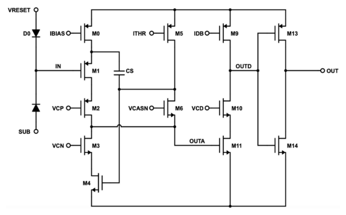
Figure 2.
(a) Image describing the second-generation CMOS monolithic pixel sensor characterization setup at IIT Madras. (b) The X-Ray irradiator, which was used to irradiate the sensor with 10 kGy of radiation.
Figure 2.
(a) Image describing the second-generation CMOS monolithic pixel sensor characterization setup at IIT Madras. (b) The X-Ray irradiator, which was used to irradiate the sensor with 10 kGy of radiation.
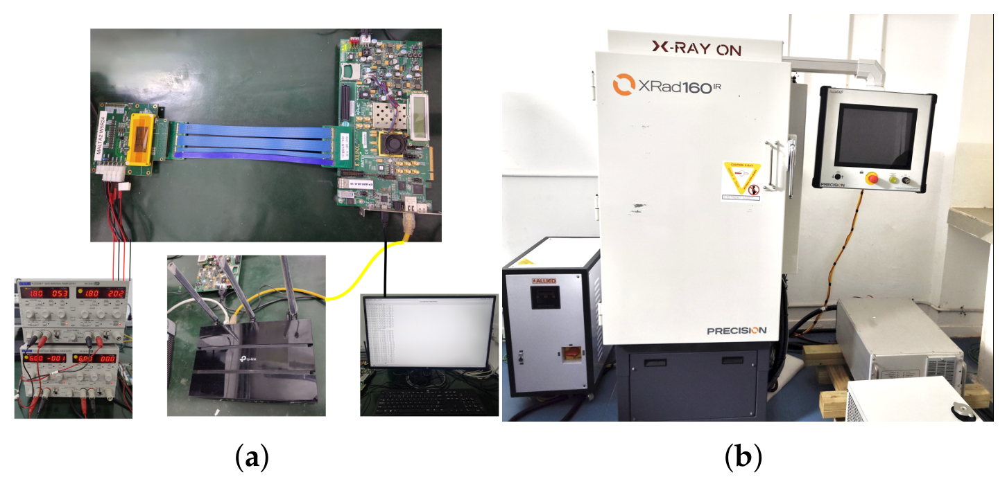
Figure 3.
(a) S-curve of an individual pixel obtained as a function of injected charge. (b) Corresponding one-dimensional threshold distribution. (c) two-dimensional distribution of threshold values within the pixel matrix.
Figure 3.
(a) S-curve of an individual pixel obtained as a function of injected charge. (b) Corresponding one-dimensional threshold distribution. (c) two-dimensional distribution of threshold values within the pixel matrix.
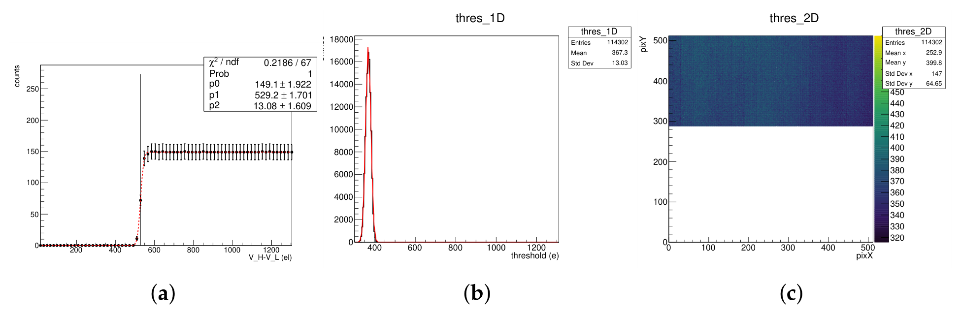
Figure 4.
Mean threshold distribution of the sensor corresponding to different values.
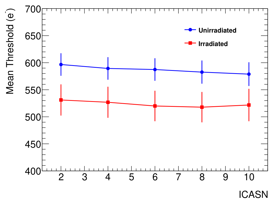
Figure 5.
Top: Two-dimensional plots showing the distribution of threshold over unirradiated and irradiated sensors. Bottom: The absolute change and percentage change of threshold values over different and values, keeping constant at 4.
Figure 5.
Top: Two-dimensional plots showing the distribution of threshold over unirradiated and irradiated sensors. Bottom: The absolute change and percentage change of threshold values over different and values, keeping constant at 4.
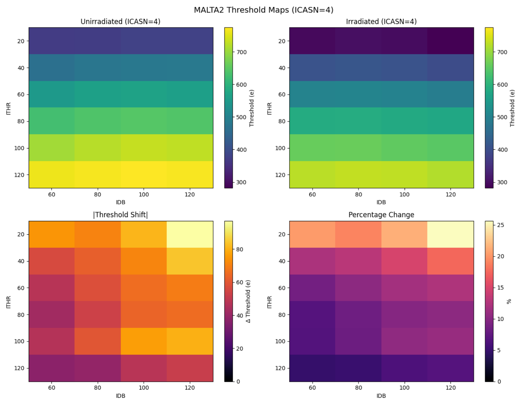
Figure 6.
Mean threshold distribution of the sensor corresponding to different values.
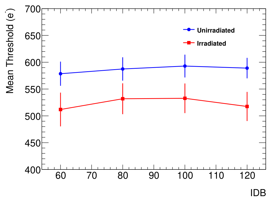
Figure 7.
Top: Two-dimensional plots showing the distribution of the threshold over unirradiated and irradiated sensors. Bottom: The absolute change and percentage change of threshold values over different and values, keeping constant at 80.
Figure 7.
Top: Two-dimensional plots showing the distribution of the threshold over unirradiated and irradiated sensors. Bottom: The absolute change and percentage change of threshold values over different and values, keeping constant at 80.
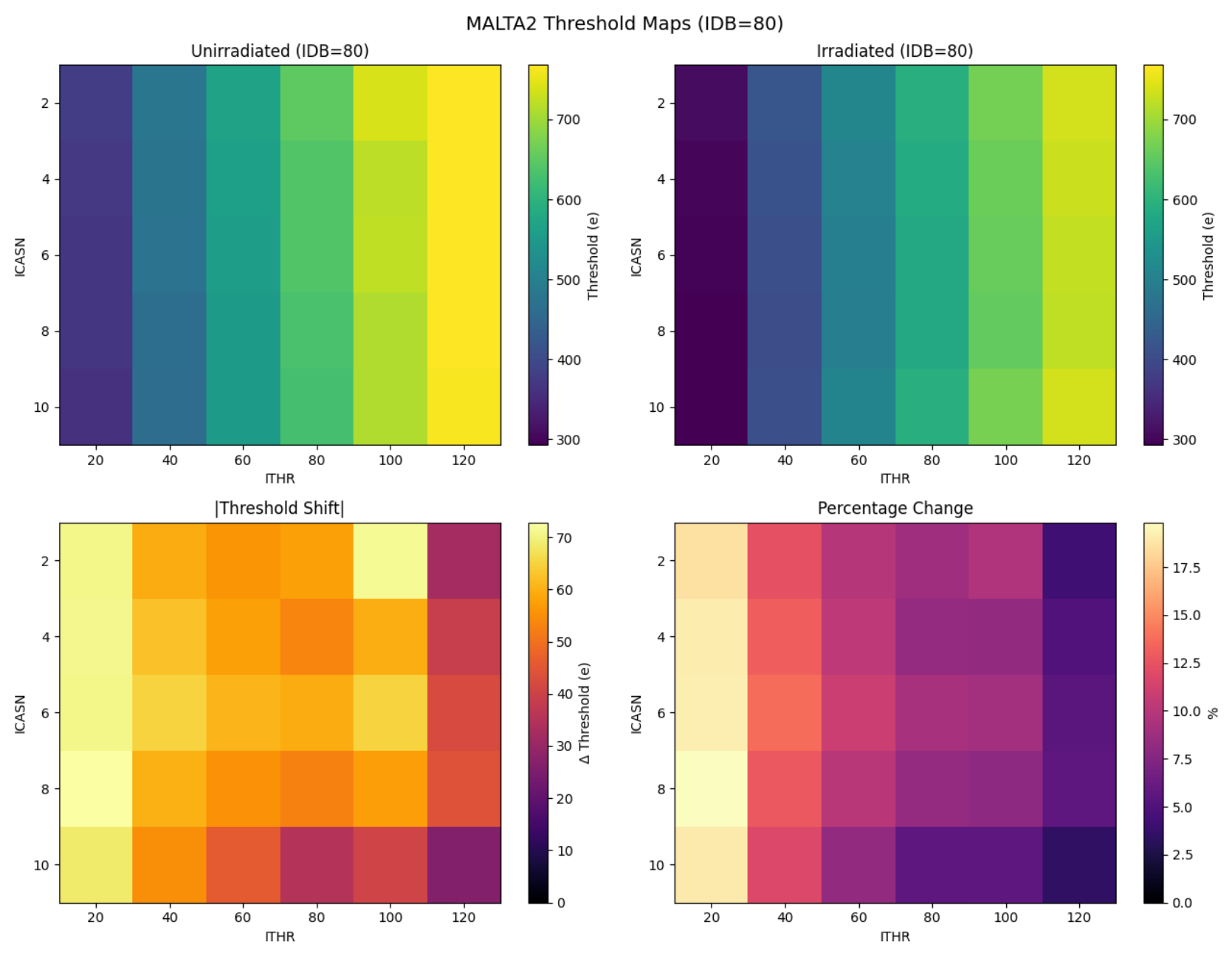
Figure 8.
Mean threshold distribution of the sensor corresponding to different values.
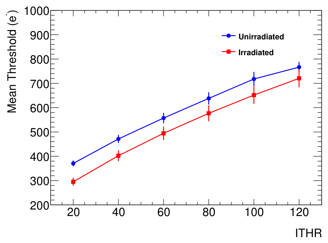
Figure 9.
Top: Two-dimensional plots representing the distribution of the threshold over unirradiated and irradiated sensors. Bottom: The absolute change and percentage change of threshold values over different and values, keeping constant at 100.
Figure 9.
Top: Two-dimensional plots representing the distribution of the threshold over unirradiated and irradiated sensors. Bottom: The absolute change and percentage change of threshold values over different and values, keeping constant at 100.
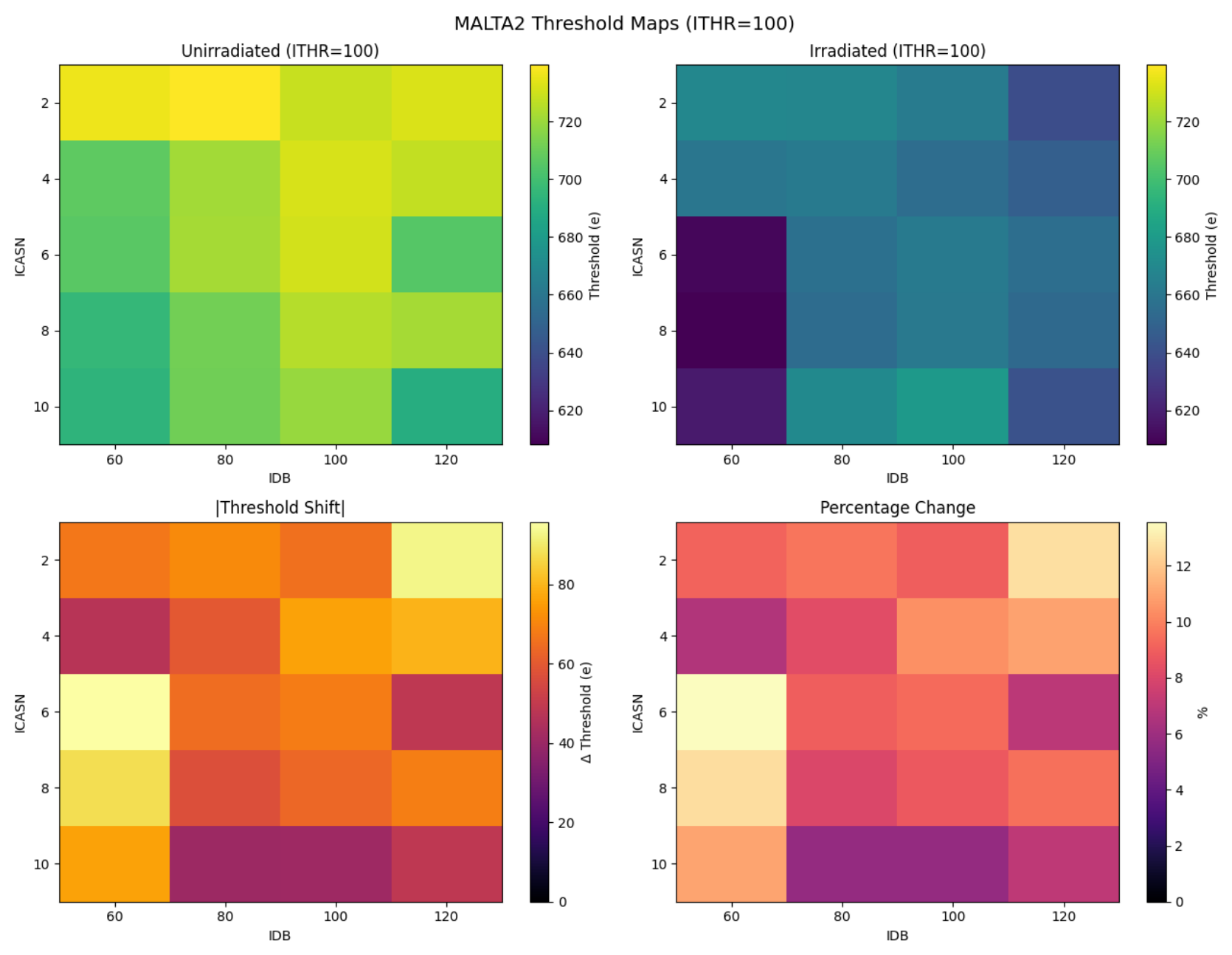
Figure 10.
(a) One-dimensional noise distribution for all pixels at , and . (b) Corresponding two-dimensional noise distribution across the pixel matrix.
Figure 10.
(a) One-dimensional noise distribution for all pixels at , and . (b) Corresponding two-dimensional noise distribution across the pixel matrix.
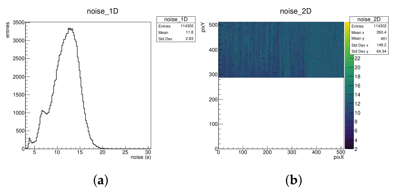
Figure 11.
Mean noise of the sensor as a function of the front-end tuning parameters: (a) , (b) , and (c) , shown for both unirradiated and irradiated conditions. The noise exhibits only a weak dependence on the tuning parameters and shows a modest increase after irradiation.
Figure 11.
Mean noise of the sensor as a function of the front-end tuning parameters: (a) , (b) , and (c) , shown for both unirradiated and irradiated conditions. The noise exhibits only a weak dependence on the tuning parameters and shows a modest increase after irradiation.
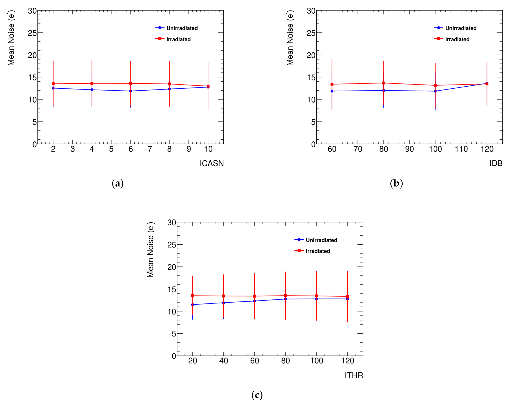
Figure 12.
Noise vs threshold plot for varying (a) (b) and (c) . For each case we varied the respective parameter, while keeping the other two DAC parameters constant.
Figure 12.
Noise vs threshold plot for varying (a) (b) and (c) . For each case we varied the respective parameter, while keeping the other two DAC parameters constant.
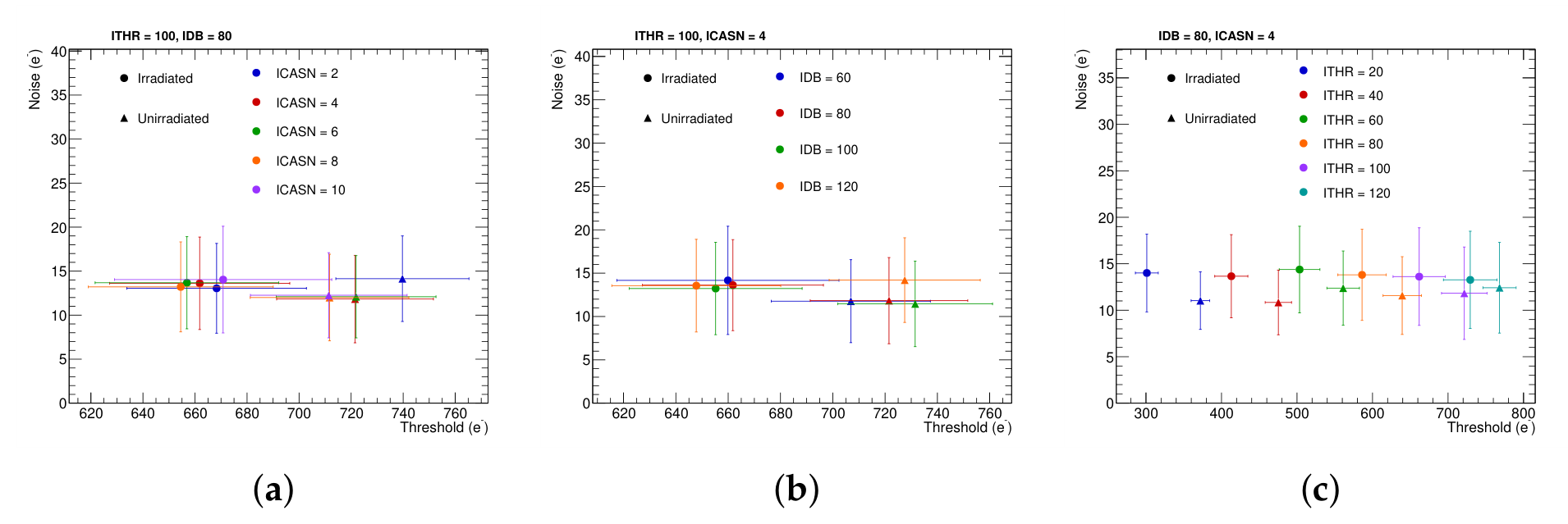
Figure 13.
Radiation-induced threshold shift as a function of the DAC parameters: (a) , (b) , and (c) . For each parameter value, the threshold shift is computed as the average difference between unirradiated and irradiated data over all configurations of the remaining parameters. A strong dependence on is observed, while shows a non-monotonic behaviour and exhibits only a weak influence.
Figure 13.
Radiation-induced threshold shift as a function of the DAC parameters: (a) , (b) , and (c) . For each parameter value, the threshold shift is computed as the average difference between unirradiated and irradiated data over all configurations of the remaining parameters. A strong dependence on is observed, while shows a non-monotonic behaviour and exhibits only a weak influence.
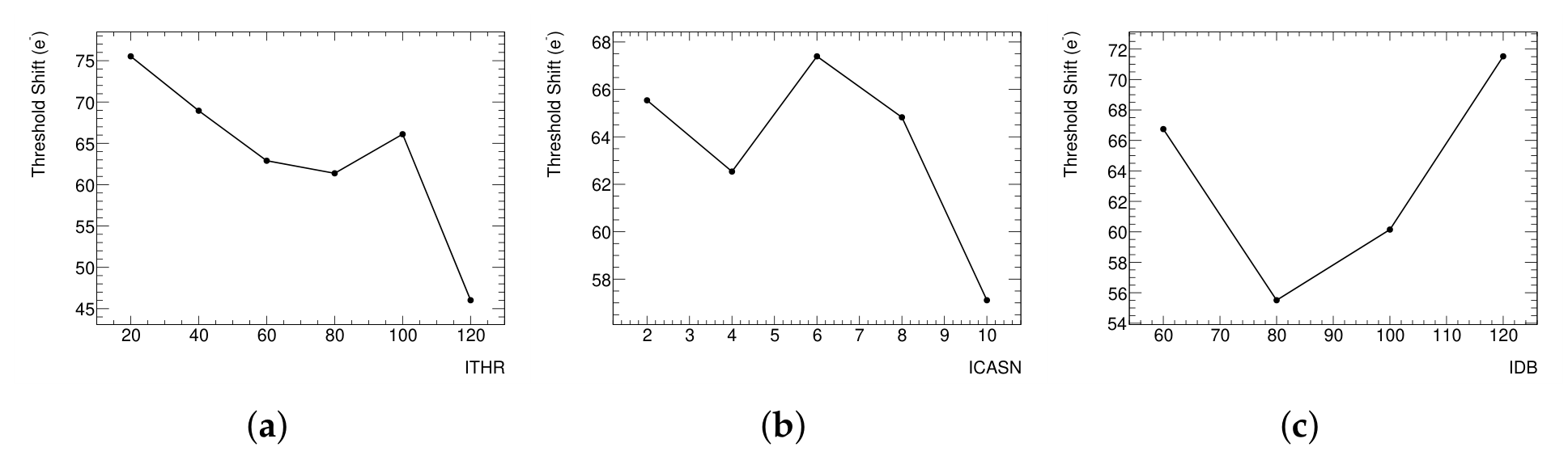

Table 1.
Description of essential DAC configurations used for threshold optimization of the sensor.
| DACs | Descriptions |
|---|---|
| "Sets the pulse duration of the amplifier output; a higher value means shorter signal and lower gain." | |
| "Sets the discriminator’s threshold; this is the main parameter for changing the threshold; a lower value means a lower threshold." | |
| "Sets the baseline of the amplifier; a higher value means a higher baseline and effectively a lower threshold charge." | |
| "Main current of the front-end; sets the power consumption, a higher value reduces the threshold and improves the speed." |
Disclaimer/Publisher’s Note: The statements, opinions and data contained in all publications are solely those of the individual author(s) and contributor(s) and not of MDPI and/or the editor(s). MDPI and/or the editor(s) disclaim responsibility for any injury to people or property resulting from any ideas, methods, instructions or products referred to in the content. |
© 2026 by the authors. Licensee MDPI, Basel, Switzerland. This article is an open access article distributed under the terms and conditions of the Creative Commons Attribution (CC BY) license (http://creativecommons.org/licenses/by/4.0/).
Copyright: This open access article is published under a Creative Commons CC BY 4.0 license, which permit the free download, distribution, and reuse, provided that the author and preprint are cited in any reuse.