Submitted:
27 May 2026
Posted:
28 May 2026
You are already at the latest version
Abstract
Image sensor chip splicing technology plays a crucial role in enhancing the imaging capabilities of current ultra-large format focal plane imaging systems for both space-based and ground-based ultra-large format focal plane imaging systems. While the imaging performance heavily relies on the flatness of the chip mounting within the splicing unit. Based on the analysis of the influencing factors of chip mounting flatness, this research developed a high flatness mounting methods for image sensor chips, irrespective of focal plane size. Through the coordinated optimization of packaging materials, structural dimensions, and mounting processes, high flatness mounting of image sensor chips can be achieved. The substrate material and thickness, along with chip size and thickness exert a more pronounced impact on chip mounting flatness compared to mounting process variables like dispensing image, adhesive thickness, and curing curve. Furthermore, for fixed substrate and chip sizes, there exists an optimal chip thickness that yields the best flatness for chip mounting. Based on this method, this research successfully achieved superior flatness mounting of a 50mm×96mm sized large format focal plane on an AIN substrate by employing both large-sized single-chip mounting and multi-small-sized chip splicing techniques. Specifically, the flatness of the large-sized single-chip mounting reached 7.9μm, while the flatness of the 2×3 chip splicing array attained 11μm.
Keywords:
image sensor
; ultra-large format focal plane
; chip splicing
; flatness
Introduction
The growing demand for more expansive imaging ranges and enhanced resolution in space-based and ground-based ultra-large format focal plane imaging systems, including remote sensing and mapping satellites, reconnaissance pods, and sky survey telescopes, necessitates the advancement of imaging systems to billions or even hundred-billion pixels [1]. This demand, in turn, propels the evolution of image sensor chips toward reduced pixel sizes and larger imaging focal plane [2,3]. Ensuring micron-level flatness of the ultra-large format focal plane composed of image sensor chips is essential for simultaneous normal imaging of all pixels. The inclination error of the CCD focal plane must be rigorously confined within the depth of focus. Failure to do so will cause part of the target surface to deviate from the image plane of the optical system, resulting in inconsistent image sharpness across the field. Consequently, the flatness requirement for the ultra-large format focal plane typically needs to reach 20μm~30μm [4,5]。
Ultra-large survey telescope at home and abroad are all implemented by means of image sensor chip unit splicing, and splicing unit are composed of large-sized single chip mounting or small-sized multiple chips splicing mounting [6,7]. Ensuring the high flatness focal plane of the splicing unit (Approximately 10μm) is essential precondition for the high flatness of the ultra-large format focal plane [8,9,10,11]. For splicing units fabricated by large-sized single chip, the mounting process is relatively straight forward. However, due to variations in material properties such as coefficient of thermal expansion (CTE) and elastic modulus, it becomes more challenging for achieving micron-level mounting flatness as the increasing chip size [12]. Additionally, the alternating effects of alternate temperature variations can induce thermal mismatch in the packaging system, resulting in flatness degradation that adversely affects imaging quality. In contrast, multiple chips splicing mounting allows for easier attainment of high flatness with smaller individual chips, but it cannot guarantee the splicing accuracy between chips and the overall flatness of the splicing units. Table 1 summarizes the flatness of ultra-large format focal plane splicing systems both domestically and internationally, in which the mounting flatness of individual chip is consistently ≤20μm [13,14,15,16,17,18,19,20,21,22].
The adhesive bonding process is currently the predominant packaging method for large-sized image sensor chips. This study investigates the high-flatness mounting process of image sensor chips for 50mm×96mm sized ultra-large format focal plane splicing units. Initially, the influence laws of the mounting process (dispensing pattern, adhesive thickness and curing curve) and packaging material (substrate material, chip size and thickness) on the flatness of chip mounting were discussed through single-chip mounting tests and finite element simulations of the splicing unit. Subsequently, based on the influence law, this research successfully achieves high-flatness format focal plane for ultra-large sized single chips and 2×3 chip arrays mounting. The work of this research enhances the comprehension of flatness control in image sensor packaging and establish a foundation for the subsequent high-flatness splicing packaging of billions or even hundred-billion pixels format focal plane.
2. Methods
2.1. Experimental Materials and Equipment
In this study, silicon wafers of varying sizes and thicknesses were utilized as chips, which were subsequently attached to Al2O3 and AlN substrates using an adhesive (Figure 1a). The Al2O3 substrate was specifically employed to attach 25mm×32mm sized chips for investigating the variation law of chip mounting flatness, while the AlN substrate was utilized for ultra-large format focal plane splicing units, attaching large-sized single chip or 2×3 chip arrays measuring 50mm×96mm. The adhesive was dispensed on the substrate using the SHOTmini100SX dispensing machine, with the dispensing pattern illustrated in Figure 1b. Subsequently, the chip attachment was executed using the MRSI-705 high-precision mounting machine, followed by curing in the ANO-640B nitrogen oven. Three curing curves are depicted in Figure 1c. For the experimentally investigation of the flatness variation law, three samples were tested for each parameter.
2.2. The Die Attachment of 2×3 Image Sensor Chip Array
Upon completion of the dispensing process on the AIN substrate, the chips of the 2×3 array are mounted in sequence. However, low flatness of the spliced unit occurred due to the height fluctuations among the chips in the array arising from mechanical errors of the chip mounter, the uniformity of the mounting pressure, and roughness deviations at different substrate positions, necessitating subsequent fine-tuning of the chip array. Finally, curing is performed according to curing curve ①.
2.3. Flatness Measurement
The Dektak-XT step gauge by Bruker Company is employed to assess the flatness of silicon wafers post-curing, applying a probe contact force of 3mg during scanning. The focal plane size of the splicing unit is 50mm×96mm. Height measurements of each point are recorded every 5μm along the X-axis, with a step length of 2mm in the Y-axis. The data are processed using the Dektak XT test software, which generates the surface profile and relevant height of the area scanned by the probe. After skew correction, a 3D map image and the flatness of the chip surface were obtained.
2.4. Finite Element Analysis of the Chip Curing Process
This thesis employs finite element simulation to model the deformation of the packaging system during the curing process, investigating the impact of substrate materials (Al2O3, AlN, SiC) on the flatness of chip mounting. To streamline the simulation, the adhesive layer was treated as a solid, and the heating process of the packaging system was simulated. Figure 2 illustrates the quarter-symmetric simulation model, which is based on the actual structure of a 2×3 image sensor splicing unit, comprising a chip, adhesive, and substrate. The intrinsic characteristic parameters of the relevant materials are presented in Table 2. The chip dimensions are 25mm×32mm, with a thickness of 400μm. The substrate thickness measures 5mm, and the surface mount dimensions are 47.5mm×96mm.
3. Results and Discussion
3.1. The Variation Law of the Chip Mounting Flatness
This study utilized a combination of process tests and finite element simulations to investigate the impact of bonding process variables (dispensing pattern, adhesive layer thickness, curing curve) and packaging material characteristics (substrate material, chip size and thickness) on the flatness of single-chip mounting and chip splicing mounting.
3.1.1. Substrate Material
The inherent differences in materials properties such as coefficient of thermal expansion (CTE) and elastic modulus lead to varying degrees of CTE mismatch between different substrates and silicon (Si) chips. Packaging systems utilizing different substrates will experience varying thermal stresses and deformations during the curing and cooling processes. This study conducted simulations to compare the impact of three substrate materials (Al2O3 ceramic, AIN ceramic, and SiC) on the flatness of chip array mounting. For the sake of simulation simplification, an mounting process involving full-surface adhesive filling, an adhesive thickness of 20μm, and a one-segment heating curve(type ① curing curve) was employed. The results are presented in Figure 3a. The deformation varies significantly as the substrate material changes. The variation in flatness primarily stems from the differences in substrate CTE, as illustrated in Figure 3b. The trend of flatness alteration is consistent with that of substrate CTE. According to the materials parameters, it can be known that the SiC substrates possess the closest thermal expansion coefficients with Si chips, followed by AlN, while the variance between Al2O3 and Si chips is the most pronounced. Consequently, this leads to minimal stress generation during the curing process of the SiC-Si system, thereby reducing chip warpage.
Additionally, substrate thickness is also a critical factor that affecting the flatness of chip mounting technology. Jiang et al. [21] simulated the impact of substrate thickness on the CMOS chips warpage, revealing that as substrate thickness increased from 1mm to 3.5mm, chip warpage decreased from 8μm to 3.5μm. In this study, the material stiffness shows a direct proportionality to the cube of the material thickness. Consequently, a thicker substrate exhibits greater flexural strength and is less susceptible to bending deformation under equivalent stress. When the chip is mounted on the substrate, a thicker substrate more effectively mitigates the chip's deformation. Thus, increasing substrate thickness proves to be an effective strategy for enhancing the chip mounting flatness.
3.1.2. Chip Size
The chip size determines the dimensions of the packaging structure. As chip size increases, the challenge of mounting flatness controlling escalates. This research experimentally compared the flatness of chips with different sizes (chip thickness 400μm, with sizes of 25mm×32mm and 50mm×96mm respectively) mounted on the same AIN substrate, the flatness measurement results are shown in Figure 4. As the chip size increases by six times, the warpage of the chip rose from 3μm to 17μm.
During the heating process, the adhesive for the chip remains in a fluid state, allowing the chip and substrate to expand freely. After being held at 150℃ for 1h, the adhesive solidifies, forming cross-linking among the chip, adhesive, and substrate. Upon cooling, the mismatch in CTE causes varying contractions in the volumes of the three components, resulting in stress accumulation. Consequently, the deformation of the chip progressively increases throughout the cooling process [23].
3.1.3. Chip Thickness
In this study, the Al2O3 substrate was utilized to experimentally assess the impact of chip thickness (200μm, 400μm, and 725μm) on the flatness of 25mm×32mm sized chips mounting. The dot matrix dispensing pattern and type ① curing curve were employed. The results are illustrated in Figure 5a. As the chip thickness increased, the warpage of the chip decreased from 8.8μm in the concave shape to 2μm in the convex shape, and then rose to 14μm in the convex shape. The flatness alteration curve is depicted in Figure 5b. By observing the concave-convex transitions of the chip, it can be inferred that there is an optimal chip thickness theoretically capable of achieving minimum chip warpage (approaching zero).
Overall, the warpage trend of chips with varying thickness is primarily affected by two factors: the inherent warpage of Si chips and the deformation that occurs during the curing process. Si chips are produced by thinning and cutting Si wafers. For chips with an initial thickness of 725µm that have not undergone thinning, the original warpage can be considered negligible, or effectively zero. In contrast, chips that have been thinned to thicknesses of 400µm and 200µm exhibit warpage within the chips, as illustrated in Figure 6. And chips of varying thicknesses exhibit varying degrees of flatness. During the chip curing process, the substrate experiences greater shrinkage deformation compared to the chip due to the difference in their coefficients of thermal expansion. For a chip with a thickness of 725µm, the chip shrinks towards the center driven by the substrate and the adhesive. However, due to the obstruction of the substrate at the chip's base, the chip can only protrude upwards. In the case of chips with thicknesses of 400µm and 200µm, upward convex deformation occurs during curing under similar forces. The deformation of the 400µm thick chip exceeds the warping of the chip, resulting in an overall upward convex morphology. Conversely, the deformation of the 200µm thick chip is less than its inherent warping, which mitigates the warping and leads to an overall concave morphology.
3.1.4. Dispensing Pattern
This study experimentally compares the influence of adhesive patterns (full-surface filling and dot matrix filling) on the chip mounting flatness. Employing a same mounting process and a type ① curing curve, the 25mm×32mm sized Si chip was mounted on the Al2O3 ceramic substrate, the flatness results are depicted in Figure 7. Both 400μm and 725μm thicknesses chips showed slight changes on the chip mounting flatness, indicating that the variation of dispensing pattern had no significant impact on the flatness of chip mounting.
The Young's modulus of the adhesive is considerably lower than that of the chip and the substrate, and it undergoes deformation with the deformation of the substrate during curing. In the packaging system described in this thesis, the substrate experiences significant shrinkage. The adhesive, which is fixed to the substrate, also shrinks in conjunction with it. Simultaneously, it applies an inward tensile force on the chip, inducing upward convex deformation of the chip. Irrespective of the adhesive's shape, its location on the substrate remains constant, and the force it exerts on the chip does not vary significantly.
3.1.5. Adhesive Layer Thickness
The impact of different adhesive layer thicknesses on the focal plane flatness of the chip was assessed. Al2O3 ceramic substrates, dot matrix dispensing process, and type ① curing curve were employed. By varying the dispensing air pressure, dot matrices of differing heights were produced, resulting in varying adhesive layer thicknesses, as illustrated in Figure 8. Specifically, adhesive dots dispensed at 40KPa exhibited inadequate filling due to the limited adhesive volume. Subsequently, the flatness of the chip was assessed under varying adhesive thicknesses.The results are illustrated in Figure 9, which suggests that adhesive thickness has minimal influence on the flatness of the mounted chips. Additionally, Jiang et al. [21] utilized finite element analysis to investigate the effect of the adhesive thickness on the flatness of a 65mm×32mm sized chip, with a thickness of 50μm. Their investigation demonstrated that as the adhesive thickness rose from 25μm to 125μm, chip warpage increased gradually from 3.4μm to 5μm, further supporting the notion that adhesive thickness has a negligible effect on chip mounting flatness.
3.1.6. Curing Curve
The research on the curing process of the adhesive primarily focuses on the heating stage due to the fixed curing temperature and holding time of the adhesive. By optimizing the heating curve (e.g., slow heating or multi-step heating), researchers aim to maximize gas release and minimize internal stress accumulation [22]. This study investigated the impact of curing curves on the flatness of chip mounting using Al2O3 ceramic substrates, Si chips with a thickness of 725μm and dimension of 32mm×25mm, and a dot matrix dispensing process. The flatness of the chips cured with the three temperature curves outlined in Table 3 was evaluated, and the results are presented in Figure 10. The findings indicate a slight decrease in chip flatness with an increasing number of temperature rise sections, suggesting that altering the temperature rise curve does not significantly enhance the flatness of the chip, nor does it substantially optimize the flatness of the splicing unit.
In conclusion, this research has developed a high flatness mounting methods for image sensor chips, regardless of its focal plane size. Through the coordinated optimization of packaging materials, structural dimensions, and mounting processes, high flatness mounting of image sensor chips can be achieved.
3.2. High Flatness Chip Mounting of Ultra-Large Format Focal Plane
Based on the preceding analysis of influencing factors, the substrate material and thickness, along with the chip size and thickness, are the primary determinants of the flatness in chip mounting. Consequently, for the ultra-large format focal plane imaging with dimension of 50mm×96mm, the high flatness mounting of ultra-large single chips and chip arrays were investigated by utilizing AIN ceramic substrates (with an increased thickness to 5mm), dot matrix dispensing patterns, and type ① temperature rise curing curves.
3.2.1. High Flatness Mounting of Ultra-Large Single Chip
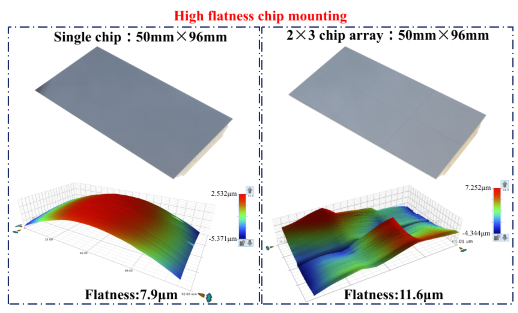
The thickness of the chip significantly influences the flatness of chip mounting. To determine the optimal mounting flatness, the relationship between chip thickness (400μm, 600μm, 725μm) and the flatness of ultra-large single chip mounting with dimension of 50mm×96mm was investigated. The results of the flatness tests are presented in Figure 11(a). As chip thickness increases, the warpage decreases from a concave 17μm to a concave 13μm, ultimately transitioning to a convex 7.9μm. This outcome demonstrates that the mounting process employed in this study can achieve micron-level flatness for ultra-large format focal plane chips. Additionally, curve fitting was performed on the flatness variation, as illustrated in Figure 11(b), revealing that the optimal chip flatness occurs at a thickness of approximately 700μm. Both the experimental findings in Figure 7 and Figure 11 suggest that for a given chip size and substrate, there exists a theoretically optimal chip thickness that facilitates the best mounting flatness, approaching zero.
3.2.2. High Flatness Mounting of Chip Arrays
Based on the analysis of the variation law of chip mounting flatness, this study utilizes 25mm×32mm sized Si chips, with a thickness of 400μm, to achieve high-flatness mounting of 2×3 image sensor chip arrays. During the curing process, the chips in the unit do not affect each other, thereby ensuring the flatness of each individual piece in the array (Figure 5). However, during the actual mounting process of the chip array, variations in factors such as the flatness of the splicing substrate, the uniformity of dispensing, and the consistency of mounting pressure lead to differences in the warpage direction and relative height among individual pieces within the splicing unit, resulting in an excessive flatness of the splicing unit. The consistency of equipment and raw materials has emerged as the primary factor affecting the flatness of the splicing unit.
By adopting the method of fine-tuning post chip array mounting to adjust the relative height variation among individual chips in the chip array, this study achieved high flatness mounting of the splicing unit. Figure 12 presents the flatness measuring results for the 2×3 image sensor splicing unit pre and post curing. The initial flatness of the splicing unit pre-curing was measured at 9.2μm, while the overall flatness after curing was recorded at 11.6μm. The measurement results also indicate that the curing process does not significantly affect the flatness of the splicing units. Furthermore, the chip array splicing method can also achieve micron-level flatness mounting with ultra-large format focal plane.
Conclusions
This thesis conducts research on the high-flatness mounting process of image sensor chips for 50mm×96mm sized ultra-large format focal plane splicing units. Through the coordinated optimization of packaging materials, structural dimensions, and mounting processes, the high flatness mounting can be achieved for image sensor chips, irrespective of its focal plane size. It is concluded that the dispensing pattern, adhesive layer thickness and curing curve are the secondary factors affecting the flatness of chip mounting, while the substrate material, thickness, chip size and thickness are the primary factors. Based on the influence law of chip thickness on the chip warpage, it is determined that when the sizes of the substrates and chips are fixed, there exists an optimal chip thickness that yields the minimum chip mounting flatness. High flatness mounting of 50mm×96mm sized single-chip or 2×3 chip splicing arrays has been achieved. Specifically, the flatness of the large-sized single chip attains 7.9μm, and the flatness of the 2×3 chip splicing array reaches 11.6μm.
Author Contributions
Hongjian Li: Methodology, Investigation, Data curation, Formal analysis, Writing–original draft. Linxiao Jing: Supervision, Writing–review & editing. Lipeng Jing: Supervision, Resources, Validation. Haoran Li: Investigation, Data curation, Validation. Qijun Zhou: Data curation. Yongchao Wu: Methodology, Conceptualization, Supervision, Data curation, Visualization, Writing–original draft.
Funding
Not applicable.
Institutional Review Board Statement
Not applicable.
Informed Consent Statement
Not applicable.
Data Availability Statement
The data that has been used is confidential.
Conflicts of Interest
The authors declare that they have no known competing financial interests or personal relationships that could have appeared to influence the work reported in this paper.
References
- Zhang, J. X. Overview of structure technologies of large aperture ground-based telescope. CHIN. OPT. 2012, 5(4), 327–336. [Google Scholar]
- Huang, F. Y.; Shen, X. J.; He, Y. Q.; et al. Performance analysis of super-wide field of view imaging system used for space target detection. Infrared Laser Eng. 2015, 44(10), 3134–3140. [Google Scholar]
- Chen, G.; Wen, Z. Q.; Qiu, C. W. Super-oscillation: from physics to optical applications. Light Sci. Appl. 2019, 8(1), 471–493. [Google Scholar] [CrossRef] [PubMed]
- Guo, N. X.; Zhang, J. X.; Liu, C. H.; et al. Overview of CCDs flatness test method for large aperture and wide-field telescope. Laser Infrared 2020, 50(4), 387–395. [Google Scholar]
- Wang, Z. Optical measurement method of angle error between CCD target surfaces and locating faces. Infrared Technol. 2012, 34(4), 213–216. [Google Scholar]
- Guo, N. X. Study on Structure Design and Flatness Metrology Method of Mosaic CCDs for Large Aperture and Wild-field View Telescope; University of Science and Technology of China, 2020. [Google Scholar]
- Niu, S. G. Research on key technologies of largr-scale focal plane splicing; University of Science and Technology of China, 2023. [Google Scholar]
- Chen, J. T. Study on CCD vacuum housing and high-precision mosaicking technology of a large focal plane array; University of Science and Technology of China, 2021. [Google Scholar]
- Liu, C. H. Key technologies of corrector lens and mosaic sensors for large aperture and wild-field telescope; Chinese Academy of Science, 2022. [Google Scholar]
- Zhang, Y.; Mo, D. F.; Li, J.; et al. Research on the thermomechanical architecture of Dewar of the large format infrared detector. Infrared Laser Eng. 2024, 53(6), 20240083. [Google Scholar]
- Yong, C. L.; Lin, J. C.; Zhao, M.; et al. Mosaic of spatial large scale CMOS focal plane array. Infrared Laser Eng. 2012, 41(10), 2561–2566. [Google Scholar]
- Niu, S. G.; Guo, L.; Lu, Z. Y.; et al. Large-scale splicing focal plane error distribution based on optical-structural-thermal integration analysis. CHIN. OPT. 2022, 15, 1000–1006. [Google Scholar]
- Zhang, Y. H. Study on Key technologies of Scientific CMOS Camera and Mosaic Focal Plane Measurement; University of Science and Technology of China, 2023. [Google Scholar]
- Wainscoat, R.; Chambers, K.; Lilly, E.; et al. The Pan-STARRS search for Near Earth Objects//2016 IEEE Aerospace Conference; IEEE, 2016; pp. 1–6. [Google Scholar]
- Kaiser, N.; Burgett, W.; Chambers, K.; et al. The Pan-STARRS wide-field optical/NIR imaging survey//Ground-based and airborne telescopes III. SPIE 2010, 7733, 159–172. [Google Scholar]
- Kamata, Y.; Miyazaki, S.; Nakaya, H.; et al. Evaluation of the fully-depleted back-illuminated CCD for Subaru Suprime-Cam//High Energy, Optical, and Infrared Detectors for Astronomy III. SPIE 2008, 7021, 547–555. [Google Scholar]
- Robbins, M. S.; Bastable, M.; Bates, A.; et al. Performance of the e2v 1.2 GPix cryogenic camera for the J-PAS 2.5m survey telescope//Ground-based and Airborne Instrumentation for Astronomy VI. SPIE 2016, 9908, 284–295. [Google Scholar]
- Gilmore, K.; Kahn, S.; Nordby, M.; et al. The LSST Camera Overview: Design and Performance//Ground-based and Airborne Instrumentation for Astronomy II. SPIE 2008, 7014, 167–177. [Google Scholar]
- Wang, Z. Y. The study of control system for wide field survey telescope prime focus mosaic camera; University of Science and Technology of China, 2024. [Google Scholar]
- Wang, L. J.; Yang, S. H. Design of sCMOS camera system. Electron. Des. Eng. 2022, 30(5), 159–164. [Google Scholar]
- Jiang, Y. Q.; Xiao, H. W.; Yang, T. Die attach evaluation for supper large CMOS image sensor chip above 60 mm. Electron. Packag. 2021, 21(4), 040202. [Google Scholar]
- Yang, F.; An, Q. C.; Zhang, J.; et al. Seeing metrology of large aperture mirror of telescope. Opt. Precis. Eng. 2017, 25(10), 2572–2579. [Google Scholar] [CrossRef]
- Sun, Z. G.; Huang, W. D.; Zhang, Q.; et al. Effect of different adhesives on the evolution of residual stress at chip surface during and after curing for COB packages. J. Funct. Mater. Devices 2002, 8(2), 195–199. [Google Scholar]
Figure 1.
(a) Substrate;(b) Dispensing pattern;(c) Curing curves.

Figure 2.
Simulation model of 2×3 image sensor splicing unit.

Figure 3.
Comparison of the flatness simulation results of the three substrates. (a) Simulation result; (b) The variation trend of the simulated deformation results and the changes in substrate CTE.
Figure 3.
Comparison of the flatness simulation results of the three substrates. (a) Simulation result; (b) The variation trend of the simulated deformation results and the changes in substrate CTE.

Figure 4.
Comparison of the flatness results of chips with different sizes mounted on AIN substrates. (a) 25mm×32mm; (b) 50mm×96mm.
Figure 4.
Comparison of the flatness results of chips with different sizes mounted on AIN substrates. (a) 25mm×32mm; (b) 50mm×96mm.

Figure 5.
The trend of flatness variation of 23mm×35mm size chips of different thicknesses. (a) Flatness measuring results; (b) Trend of flatness change.
Figure 5.
The trend of flatness variation of 23mm×35mm size chips of different thicknesses. (a) Flatness measuring results; (b) Trend of flatness change.

Figure 6.
The warpage of the chips post-thinning and cutting. (a) 200µm thickness chip; (b) 400µm thickness chip.
Figure 6.
The warpage of the chips post-thinning and cutting. (a) 200µm thickness chip; (b) 400µm thickness chip.

Figure 7.
The influence of dispensing patterns on the flatness of single-chip mounting on Al2O3 substrates.
Figure 7.
The influence of dispensing patterns on the flatness of single-chip mounting on Al2O3 substrates.

Figure 8.
The morphology of the adhesive dots under different dispensing pressures and the morphology of the adhesive dots after chip mounting under X-ray scanning. (a) 130KPa; (b) 80KPa; (c) 40KPa.
Figure 8.
The morphology of the adhesive dots under different dispensing pressures and the morphology of the adhesive dots after chip mounting under X-ray scanning. (a) 130KPa; (b) 80KPa; (c) 40KPa.

Figure 9.
The variation trend of chip flatness with the thickness of the adhesive layer.

Figure 10.
The influence of curing curves on the flatness of single-chip mounting on Al2O3 substrates.
Figure 10.
The influence of curing curves on the flatness of single-chip mounting on Al2O3 substrates.

Figure 11.
The flatness changing trend of the 50mm×96mm sized chips with different thicknesses on the AIN substrate. (a) Flatness measuring results; (b) Trend of flatness change; (c) Morphology of the ultra-large single chip post-curing.
Figure 11.
The flatness changing trend of the 50mm×96mm sized chips with different thicknesses on the AIN substrate. (a) Flatness measuring results; (b) Trend of flatness change; (c) Morphology of the ultra-large single chip post-curing.

Figure 12.
Flatness of the 2×3 image sensor chip array after fine-tuning. (a) Morphology of the chip array pre-curing; (b) The flatness measurement of the chip array prior to curing; (c) The flatness measurement of the chip array post-curing.
Figure 12.
Flatness of the 2×3 image sensor chip array after fine-tuning. (a) Morphology of the chip array pre-curing; (b) The flatness measurement of the chip array prior to curing; (c) The flatness measurement of the chip array post-curing.


Table 1.
Focal plane flatness specifications for the splicing sensor chips in large-scale optical survey telescopes worldwide [13].
Table 1.
Focal plane flatness specifications for the splicing sensor chips in large-scale optical survey telescopes worldwide [13].
| Survey telescopes | CCD types | CCD numbers | Dimension of the CCDs | Nominal PV of the CCDs | PV of the overall focal plane |
| Pan-STARRS [14,15] |
CCID58 | 60 | 50mm×50mm | 10μm | 40μm |
| Subaru/HSC [16] | CCID-20 | 116 | 30.72mm×61.44mm | 20μm | 34μm |
| SkyMapper | CCD44-82 | 32 | 30.72mm×61.44mm | 20μm | 64μm |
| J-PAS/JPCam [17] | CCD290-99 | 14 | 92.2mm×92.4mm | 15μm | 27μm |
| LSST [18] | CCD250-82 | 189 | 42mm×42mm | 7μm | 22μm |
| WFST [19] | CCD290-99 | 9 | 92.2mm×92.4mm | 15μm | 20μm |
| HFMC-Cam [20] | GSENSE6060 | 25 | 61mm×61mm | <10μm | <20μm |
| / | [21] | / | 62mm×32mm | <10μm | / |
Table 2.
Materials and the parameters.
| Materials | CTE(10-6·℃-1) | Young's modulus(GPa) | poisson ratio |
thermal conductivity (W/mˑK) |
| Al2O3 | 6.7 | 350 | 0.1 | 25 |
| AlN | 4.4 | 320 | 0.23 | 200 |
| SiC | 2 | 450 | 0.14 | 180 |
| Si | 2.6 | 187 | 0.2 | 150 |
| Adhesive | 33 | 10 | 0.38 | 1 |
Disclaimer/Publisher’s Note: The statements, opinions and data contained in all publications are solely those of the individual author(s) and contributor(s) and not of MDPI and/or the editor(s). MDPI and/or the editor(s) disclaim responsibility for any injury to people or property resulting from any ideas, methods, instructions or products referred to in the content. |
© 2026 by the authors. Licensee MDPI, Basel, Switzerland. This article is an open access article distributed under the terms and conditions of the Creative Commons Attribution (CC BY) license (http://creativecommons.org/licenses/by/4.0/).
Copyright: This open access article is published under a Creative Commons CC BY 4.0 license, which permit the free download, distribution, and reuse, provided that the author and preprint are cited in any reuse.


