

Submitted:
04 May 2026
Posted:
05 May 2026
You are already at the latest version
Abstract
The integration density of photonic integrated circuits is fundamentally limited by evanescent field overlap and subsequent inter-channel crosstalk. Layered transition metal dichalcogenides (TMDCs) bypass these confinement constraints through intrinsic optical birefringence and high refractive indices. Here, we report the near-infrared optical constants and waveguide dispersion of molybdenum diselenide (MoSe2). Ellipsometry performed on centimeter-scale crystals yields an in-plane refractive index of 4.1–4.7 over 1000–2000 nm, with an extinction coefficient close to the sensitivity limit of the fit away from strong excitonic resonances. To validate the anisotropic dielectric tensor at the device scale, scattering-type scanning near-field optical microscopy (s-SNOM) was utilized to map the propagation of transverse-magnetic modes in 235-nm-thick exfoliated flakes. Spatial Fourier analysis of the edge-scattered near-field interference yields effective mode indices that precisely match the modeled dispersion. Using the verified dielectric tensor, finite-element simulations demonstrate that single-mode MoSe2 waveguides optically outperform equivalent tungsten disulfide (WS2) benchmarks. The enhanced evanescent field suppression in the claddings of MoSe2 waveguide increases the coupling length by a factor of 3.5, reducing the required routing pitch and enabling a 12.5% direct increase in on-chip integration density. The results identify MoSe2 as a high-index anisotropic platform for compact waveguiding in the near-infrared.
Keywords:
molybdenum diselenide
; transition metal dichalcogenides
; van der Waals materials
; anisotropic optical constants
; spectroscopic ellipsometry
; scanning near-field optical microscopy
; integrated photonics
; waveguide crosstalk
1. Introduction
Dense photonic integrated circuits require tight optical confinement to minimize individual device footprints [1,2]. In conventional isotropic platforms, such as silicon and silicon nitride, physical scaling is bottlenecked by evanescent field leakage, which causes severe optical crosstalk at sub-wavelength routing pitches [3]. Layered van der Waals (vdW) materials with a strong in-plane covalent bonding and weak out-of-plane vdW forces, offer a structural solution to this confinement limit [4]. VdW materials have become a central materials class in modern nanophotonics because they combine strong light–matter interaction with crystallographically defined optical anisotropy and broad compatibility with heterogeneous integration [2,3,5,6,7,8]. Within this family, transition metal dichalcogenides (TMDCs) are especially relevant for guided-wave and resonant nanophotonics because bulk and multilayer crystals can simultaneously provide a high refractive index, giant uniaxial optical birefringence, and low loss over selected spectral windows [4,9,10,11,12,13,14]. From an integrated photonics perspective, these properties are not only of fundamental interest. The refractive-index contrast and the anisotropic dielectric response directly determine modal confinement, single-mode design limitations, evanescent-field penetration, and the strength of coupling between adjacent optical channels [5,9,15,16]. As a result, reliable optical constants in the near-infrared around the telecommunication band are crucial for realistic benchmarking of TMDC waveguides, couplers, and other building blocks of photonic integrated circuits.
Molybdenum diselenide (MoSe2) is a particularly interesting material of the high-index TMDC class [5,17]. Prior studies have established that MoSe2 can sustain guided exciton–polariton transport in crystal flake waveguides closer to the visible and excitonic spectral range, highly-confined optical modes and high nonlinear response in epitaxially grown MoSe2 in near-infrared range [12,18,19]. The combination of a high in-plane refractive index (nab > 4), low absorption, and giant optical anisotropy, birefringence Δn = nab − nc ~ 1, in crystal bulk MoSe2 enables the localization of the electromagnetic field at subwavelength scales and provides a single-mode operation in compact photonic waveguides [4,5,9,20,21]. In this regard, the design of low-loss near-infrared photonic components requires a device-oriented description that links anisotropic optical constants, experimentally observed guided modes, and engineering figures of merit such as coupling length. However, determination of the dielectric permittivity of vdW crystals is a non-trivial, since the studied samples, microcrystals, i.e., flakes, obtained by mechanical exfoliation from the original crystal, often have dimensions of up to several tens of micrometers [22,23,24]. This restricts the utilization of traditional methods such as spectroscopic ellipsometry and reflectometry for determining the optical constants over a wide spectral range. Moreover, these far-field optical methods have low sensitivity to determine the out-of-plane component of refractive index (nc) [10,17]. In contrast, scattering-type scanning near-field optical microscopy (s-SNOM) enables local measurement of the optical response, excitation and propagation of guided modes in vdW materials with spatial resolution exceeding the diffraction limit and allows verification of the numerical values of the anisotropy of optical constants obtained independently, using spectroscopic ellipsometry [9,10,16,24,25,26].
In this work, we present a detailed characterization of the optical constants and waveguide properties of the high-index crystal MoSe2 in the near-infrared by combining the macroscopic spectroscopic ellipsometry, s-SNOM, and electromagnetic modeling to build and test an anisotropic optical model demonstrating the applications of MoSe2 in nanophotonics. First, we extract the in-plane optical constants of a macroscopic crystal in the 1000–2000 nm range. Next, we visualize guided TM modes in an exfoliated MoSe2 flake and compare the measured modal dispersion with transfer-matrix calculations. Finally, we use the experimentally supported model to benchmark ridge MoSe2 waveguides against WS2 counterparts in the single-mode regime.
2. Materials and Methods
2.1. Material Preparation and Morphological Characterization
A commercially available ultra-flat large-area bulk MoSe2 crystal grown by chemical vapor transport (CVT, 2D Semiconductors, Inc., USA) was used for ellipsometric characterization. The crystal composition was examined by energy-dispersive X-ray spectroscopy (EDS, Bruker QUANTAX EDX) in a scanning electron microscope setup (SEM, JEOL JSM-7001F) working in secondary electron imaging mode. The value of the acceleration voltage was 15 keV. The EDS spectrum was analyzed using the software provided by Bruker. For near-field measurements, MoSe2 flakes were obtained by mechanical exfoliation from the same parent crystal and transferred onto a SiO2(285nm)/Si substrate. Optical microscopy was used to identify flakes of sufficient lateral size, and atomic force microscopy (AFM, NT-MDT Spectrum Instruments) in contact mode was used to determine the flake thickness. The cantilevers employed were NSA01 tips (TipsNano), characterized by a spring constant of 5.1 N/m, a tip radius of less than 10 nm, and a resonant frequency of 150 kHz. Analysis of AFM scans was performed using Gwyddion software.
2.2. Spectroscopic Ellipsometry
The optical constants of the macroscopic MoSe2 crystal were measured with a variable-angle spectroscopic ellipsometer (V-VASE, J.A. Woollam Co.) in the wavelength range 1000–2000 nm. A large-area crystal (~1 cm2) was required because the ellipsometer spot size was approximately ~1.5 mm. The ellipsometric parameters Ψ and Δ were recorded in reflection geometry at incidence angles of 50°, 55°, and 60° with a wavelength step of 5 nm. The data were fitted in WVASE using a parallel-sided slab model that included backside reflection. The dielectric response was parameterized with the Tauc–Lorentz dispersion model, which preserves the Kramers–Kronig consistency and has been broadly used for TMDC optical constants extraction [5,12,20,21].
2.3. Scattering-Type Scanning Near-Field Optical Microscopy
Near-field imaging of guided modes was performed with a commercial s-SNOM system (neaSNOM, Neaspec GmbH) operated in reflection mode. A tunable continuous-wave fiber-coupled laser (Agilent 81600B) with a range of 1460–1640 nm was used as the excitation source. The optical probe was a metalized AFM tip (NanoWorld, ARROW-NCPt-50) oscillating at Ω ≈ 280 kHz. A pseudo-heterodyne interferometric scheme was employed, and the detector signal was demodulated third harmonic to isolate the background-suppressed near-field amplitude and phase [27]. The excitation polarization was chosen to launch TM-polarized guided modes in the flake. To select a suitable planar waveguide thickness, the TM-mode dispersion of the MoSe2/SiO2/Si stack was first evaluated by the transfer-matrix method [28,29] for the measured in-plane response and the adopted out-of-plane refractive index.
The near-field fringe pattern was analyzed in the Fourier domain using line profiles extracted perpendicularly to the flake edge. In accordance with the established interpretation of guided-mode s-SNOM in anisotropic TMDCs flakes, the observed pattern is attributed to interference between the incident field and a tip-launched guided mode that is scattered at the flake boundary. The Fourier peak position yields the apparent normalized in-plane momentum ns-SNOM. The effective mode index was then extracted as , where α is the angle between the illumination wavevector and its projection onto the sample plane, and β is the angle between the in-plane projection and the flake edge. For the present geometry, α = 45° and β = 90°.
2.4. Numerical Modeling
Ridge waveguides with MoSe2 or WS2 cores on a SiO2 substrate and air cladding were analyzed using the finite-element method in COMSOL Multiphysics. The crystal optic axis was assumed to be normal to the substrate, consistent with the layered-flake geometry. To quantify coupling between neighboring waveguides, even and odd supermodes of a coupled-waveguide pair were calculated for different center-to-center spacings d. The coupling length was then obtained from [30]
Coupling length was optimized at core widths and heights, at which waveguide operates in the single-mode regime.
3. Results and Discussion
For the initial determination of the in-plane optical constants, spectroscopic ellipsometry was applied to the molybdenum diselenide (MoSe2) crystal. Measurements were performed using a Woollam V-VASE ellipsometer in the wavelength range λ = 1000–2000 nm, which is important for telecommunications applications. A large-area crystal (~1 cm²), synthesized by CVT, was chosen as the MoSe2 sample. In the experiment, the choice of a macroscopic crystal was dictated by the minimum spot size of the ellipsometer measurement beam, which is approximately ~1.5 mm in diameter. Measurements of the ellipsometric parameters Ψ and Δ were performed in reflection mode (see Methods). To determine the in-plane refractive index nab and extinction coefficient kab of the MoSe2 crystal, a layered model including backside reflection was used. For the dielectric function, the Tauc–Lorentz oscillator dispersion model was employed in fitting the Ψ and Δ spectra, providing analytical satisfaction of the Kramers–Kronig relations, similarly to approaches used for other TMDCs, using the WVASE software [9,10,20,21]. The results of the ellipsometry data analysis for MoSe2 are presented in Figure 1a. The in-plane refractive index nab varies smoothly in the range of 4.1–4.7, while the extinction coefficient kab is close to zero within the sensitivity of the ellipsometer, remaining well above the values typical of conventional dielectric photonic materials in the near-infrared [5,10,22]. Since the ellipsometry methodology used in this work is limited to determining optical constants within an isotropic model, to account for anisotropy for further investigation of the waveguide properties of MoSe2, the out-of-plane refractive index nc from reference [12] was used.
The s-SNOM technique allows for the independent verification of the optical constants of vdW crystals and confirmation of the magnitude of optical anisotropy, s-SNOM was used to measure the propagation of photonic modes in MoSe2 [10,21]. To this end, planar waveguides were fabricated by mechanically exfoliating MoSe₂ flakes onto a SiO2(285 nm)/Si substrate from a macroscopic crystal. Suitable MoSe2 flakes with sufficient area and the required thickness for the propagation of the fundamental photonic TM mode in the wavelength range near 1500 nm were identified using optical microscopy and AFM. The range of thicknesses required for the propagation of a single TM mode was determined by numerical calculation using the transfer matrix method [28] and the optical constants of MoSe2 in Figure 1a, yielding thickness values from 200 to 370 nm. This choice is important because it enables a direct comparison between measured and calculated modal dispersion without the ambiguity introduced by higher-order guided states. The AFM step profile on a chosen flake yielded a thickness of 235 ± 5 nm (see inset in Figure 1c), which falls inside the calculated single-mode interval for the planar TM mode near λ = 1.5 μm and was selected for s-SNOM measurements. In addition, the EDS spectrum in Figure 1b confirms the expected stoichiometry of the parent crystal, with measured atomic fractions of 34.7% for Mo and 65.3% for Se, corresponding closely to the 1:2 composition of MoSe2.
Next, to study photonic modes in MoSe2 planar waveguides, the s-SNOM metallic tip is illuminated with laser radiation in the 1460–1640 nm range in TM polarization (see Section 2.3 for more details). Scanning the tip perpendicular to the crystal edge allows mapping of interference fringes. The resulting s-SNOM amplitude and phase images recorded near the flake edge at wavelengths of 1475 and 1625 nm are shown in Figure 2a. Both wavelengths reveal a clear sequence of near-field fringes extending inward from the flake boundary, which is consistent with the excitation of a guided TM0 mode in the planar MoSe2 waveguide. The fringe periodicity is directly related to the mode wavelength (λp) and, consequently, to the effective mode index (neff = λ0/λp, where λ0 is the free-space wavelength). The effective refractive index of the propagating TM mode in an anisotropic planar MoSe2 waveguide depends on both the in-plane (nab) and out-of-plane (nc) refractive indices. Thus, by determining neff and comparing it with theoretical calculations of the dispersion curve using the transfer matrix method, it is possible to verify the anisotropic optical constants. To determine neff, complex fast Fourier transform of line profiles extracted from the near-field images was performed and the corresponding Fourier spectra are shown in Figure 2b. The dominant peaks (at q(k0) ~ 1.1) assigned to the TM₀ mode were used to determine the in-plane modal momenta, while additional peaks in the Fourier spectra arise due to the propagation of the wave in air and do not affect the position of the peak corresponding to the desired TM0 mode After applying the geometric frequency shift described in Section 2.3, the extracted effective indices at 1475 and 1625 nm were compared with transfer-matrix calculations of the energy (E~1/λ0)-momentum (q=1/λp) dispersion relation of the waveguide mode for the anisotropic MoSe2/SiO2/Si stack. As shown in Figure 2c, the experimental effective indices points follow the calculated dispersion curve. This agreement does not by itself constitute a full independent reconstruction of the complete dielectric tensor, because the out-of-plane response was taken from literature, but it does provide an important consistency check: the measured in-plane optical constants nab and kab, the adopted nc, and the flake thickness together describe the observed guided-mode dispersion without the need for further adjustable parameters.
Using the experimentally supported optical model, we next evaluated the prospects of using MoSe2 in nanophotonics, by numerical modeling of the behavior of waveguides based on this material. Characteristics of MoSe2 waveguides were compared with those of WS2, another TMDC with a high refractive index and optical anisotropy, whose waveguiding performance has previously been shown to be better than silicon, the backbone material of modern nanophotonics [9]. First, the effective indices of the supported waveguide modes were calculated (see Methods). This allowed determination of the number of supported waveguide modes as a function of the waveguide core width (w) and height (h), as well as the construction of effective index maps for the fundamental mode, i.e., the mode with the highest index. From the nanophotonic viewpoint, the effective index is an important parameter characterizing the degree of field confinement within the waveguide core. In particular, it determines the size of resonators and modulators, and also governs radiation losses in bent waveguide sections. Furthermore, the higher the effective index, the faster the evanescent field decays in the waveguide cladding, leading to reduced crostalk between adjacent waveguides and, consequently, enabling denser integration of waveguides on a chip, thereby enhancing the performance of photonic integrated circuits [9]. In Figure 3 comparison of the effective-index maps for MoSe2 and WS2 rectangular waveguides show that MoSe2 core supports modes with a higher effective index at smaller core dimensions, which is expected due to the higher refractive index of MoSe2. On the other hand, for equal dimensions, MoSe2 waveguides support more modes, whereas in practice a single-mode regime is important, as it allows better control of signal transmission through the waveguide. Nevertheless, in the single-mode regime, i.e., at smaller core dimensions, MoSe2 waveguides exhibit a higher effective index than WS2 waveguides, suggesting weaker crosstalk compared to WS2.
To test this hypothesis, the coupling length Lc, which characterizes the mutual influence of adjacent waveguides, was calculated. After propagating this distance along the waveguide, the mode completely transfers from one waveguide to the neighboring one (see Methods for the details on crosstalk calculations). The calculation results show that for a fixed waveguide core width w, Lc increases with core height; therefore, the optimal core dimensions should lie on the cutoff curve of the second waveguide mode (the white curve in Figure 3). For a fixed center-to-center distance d = 1 μm between waveguides, the maximum achievable coupling length Lc for MoSe2 waveguides exceeds 15 mm, which is approximately 3.5 times higher than the same value for WS2 waveguides, which is 4.3 mm.
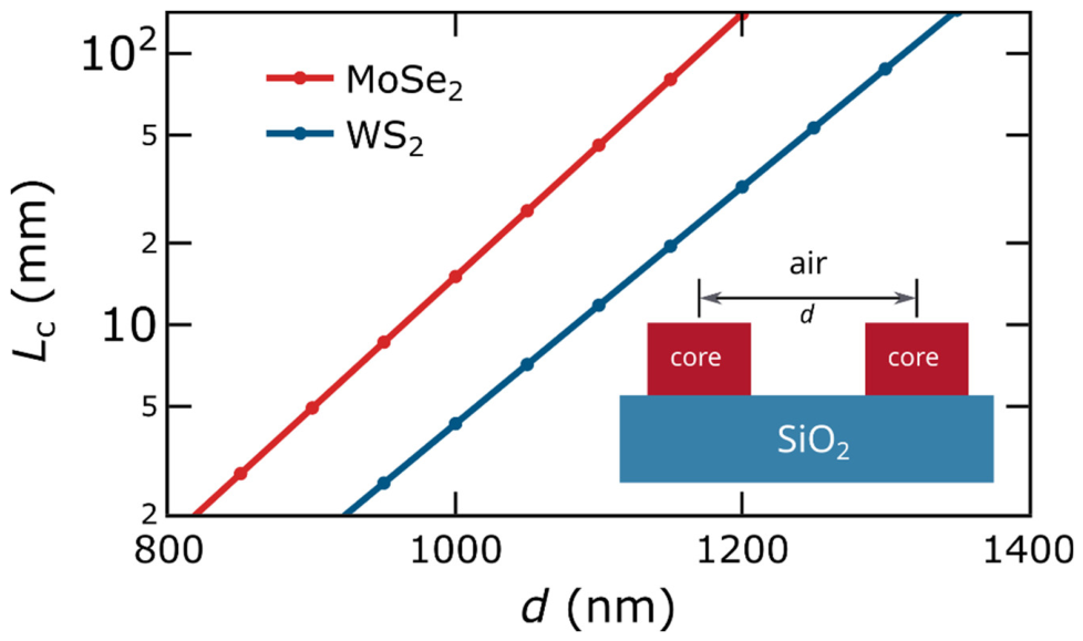
A more detailed investigation of the dependence of Lc on d (Figure 4) shows that the advantage of MoSe2 over WS2 increases as the distance between waveguides grows. At the same time, if we compare the minimum distance between waveguides at which Lc = 10 mm, which is sufficient for constructing global interconnects on a chip, then MoSe2 (dmin = 960 nm) outperforms WS2 (dmin = 1080 nm) by 12.5%. This enhancement is very significant and hard to achieve considering the near-exponential dependence of the coupling length on the distance between waveguides, which is caused by the exponential decay of the waveguide mode field outside the waveguide core. Moreover, there exist methods for further increasing integration density by engineering the space between waveguides, which can not only reduce the distance between waveguides but also almost completely suppress waveguide coupling [30,31].
4. Conclusions
We have evaluated bulk-like MoSe2 as a near-infrared waveguiding material by combining spectroscopic ellipsometry, s-SNOM near-field imaging, and electromagnetic modeling. The fitted in-plane refractive index remains between 4.1 and 4.7 from 1000 to 2000 nm, while the fitted extinction coefficient is close to zero within the sensitivity of the fit. Guided TM0 modes imaged at 1475 and 1625 nm yield effective indices consistent with transfer-matrix calculations based on the measured in-plane response, the measured flake thickness, and a literature out-of-plane index. This agreement supports the internal consistency of the anisotropic optical model. Waveguide benchmarking further showed that, in the single-mode regime, MoSe2 provides higher effective indices and longer coupling lengths than another high-refractive-index anisotropic material WS2. This leads to a reduction in crosstalk by approximately a factor of 3.5, demonstrating that MoSe2 waveguides are more compact and effective, which can be used to increase the integration density and reliability of photonic circuits. These results support MoSe2 as a high-index anisotropic material platform for compact near-infrared photonic routing.
Author Contributions
D.Y., A.V., and D.G. contributed equally to this work. G.E., A.V., A.A., and V.V. suggested and directed the project. D.Y., B.K., M.T., and T.K. performed the measurements and analyzed the data. D.G. and A.V. provided theoretical support. A.V., D.Y., D.G., A.A., and V.V. wrote the original manuscript. All authors reviewed and edited the paper. All authors contributed to the discussions and commented on the paper.
Data Availability Statement
The datasets measured and analysed during the current study are available from the corresponding author upon reasonable request.
Acknowledgments
A.V. and D.Y. gratefully acknowledge the financial support from the RSF (Grant No. 24-72-10039).
Conflicts of Interest
Authors Andrey Vyshnevyy, Dmitry Grudinin, Aleksey Arsenin and Valentyn Volkov were employed by the company XPANCEO. The remaining authors declare that the research was conducted in the absence of any commercial or financial relationships that could be construed as a potential conflict of interest.
References
- Bogaerts, W.; Pérez, D.; Capmany, J.; Miller, D.A.B.; Poon, J.; Englund, D.; Morichetti, F.; Melloni, A. Programmable Photonic Circuits. Nature 2020, 586, 207–216. [Google Scholar] [CrossRef]
- de Abajo, F.J.G.; Basov, D.N.; Koppens, F.H.L.; Orsini, L.; Ceccanti, M.; Castilla, S.; Cavicchi, L.; Polini, M.; Gonçalves, P.A.D.; Costa, A.T.; et al. Roadmap for Photonics with 2D Materials. ACS Photonics 2025, 12, 3961–4095. [Google Scholar] [CrossRef]
- Song, S.; Rahaman, M.; Jariwala, D. Can 2D Semiconductors Be Game-Changers for Nanoelectronics and Photonics? ACS Nano 2024, 18, 10955–10978. [Google Scholar] [CrossRef]
- Ling, H.; Li, R.; Davoyan, A.R. All van Der Waals Integrated Nanophotonics with Bulk Transition Metal Dichalcogenides. ACS Photonics 2021, 8, 721–730. [Google Scholar] [CrossRef]
- Zotev, P.G.; Wang, Y.; Andres-Penares, D.; Severs-Millard, T.; Randerson, S.; Hu, X.; Sortino, L.; Louca, C.; Brotons-Gisbert, M.; Huq, T.; et al. Van Der Waals Materials for Applications in Nanophotonics. Laser Photon. Rev. 2023, 17, 2200957. [Google Scholar] [CrossRef]
- Feng, Y.; Chen, R.; He, J.; Qi, L.; Zhang, Y.; Sun, T.; Zhu, X.; Liu, W.; Ma, W.; Shen, W.; et al. Visible to Mid-Infrared Giant in-Plane Optical Anisotropy in Ternary van Der Waals Crystals. Nat. Commun. 2023, 14, 6739. [Google Scholar] [CrossRef]
- Ma, G.; Shen, W.; Sanchez, D.S.; Yu, Y.; Wang, H.; Sun, L.; Wang, X.; Hu, C. Excitons Enabled Topological Phase Singularity in a Single Atomic Layer. ACS Nano 2023, 17, 17751–17760. [Google Scholar] [CrossRef] [PubMed]
- Grudinin, D.V.; Ermolaev, G.A.; Baranov, D.G.; Toksumakov, A.N.; Voronin, K.V.; Slavich, A.S.; Vyshnevyy, A.A.; Mazitov, A.B.; Kruglov, I.A.; Ghazaryan, D.A.; et al. Hexagonal Boron Nitride Nanophotonics: A Record-Breaking Material for the Ultraviolet and Visible Spectral Ranges. Mater. Horiz. 2023, 10, 2427–2435. [Google Scholar] [CrossRef] [PubMed]
- Vyshnevyy, A.A.; Ermolaev, G.A.; Grudinin, D.V.; Voronin, K.V.; Kharichkin, I.; Mazitov, A.; Kruglov, I.A.; Yakubovsky, D.I.; Mishra, P.; Kirtaev, R.V.; et al. Van Der Waals Materials for Overcoming Fundamental Limitations in Photonic Integrated Circuitry. Nano Lett. 2023, 23, 8057–8064. [Google Scholar] [CrossRef]
- Ermolaev, G.A.; Grudinin, D.V.; Stebunov, Y.V.; Voronin, K.V.; Kravets, V.G.; Duan, J.; Mazitov, A.B.; Tselikov, G.I.; Bylinkin, A.; Yakubovsky, D.I.; et al. Giant Optical Anisotropy in Transition Metal Dichalcogenides for next-Generation Photonics. Nat. Commun. 2021, 12, 854. [Google Scholar] [CrossRef]
- Khurgin, J.B. Expanding the Photonic Palette: Exploring High Index Materials. ACS Photonics 2022, 9, 743–751. [Google Scholar] [CrossRef]
- Munkhbat, B.; Wróbel, P.; Antosiewicz, T.J.; Shegai, T.O. Optical Constants of Several Multilayer Transition Metal Dichalcogenides Measured by Spectroscopic Ellipsometry in the 300-1700 Nm Range: High Index, Anisotropy, and Hyperbolicity. ACS Photonics 2022, 9, 2398–2407. [Google Scholar] [CrossRef]
- Zograf, G.; Polyakov, A.Y.; Bancerek, M.; Antosiewicz, T.J.; Küçüköz, B.; Shegai, T.O. Combining Ultrahigh Index with Exceptional Nonlinearity in Resonant Transition Metal Dichalcogenide Nanodisks. Nat. Photonics 2024, 18, 751–757. [Google Scholar] [CrossRef]
- Nørgaard, M.; Yezekyan, T.; Rolfs, S.; Frydendahl, C.; Mortensen, N.A.; Zenin, V.A. Near-Field Refractometry of van Der Waals Crystals. Nanophotonics 2025, 14, 2473–2483. [Google Scholar] [CrossRef] [PubMed]
- Zotev, P.G.; Bouteyre, P.; Wang, Y.; Randerson, S.A.; Hu, X.; Sortino, L.; Wang, Y.; Shegai, T.; Gong, S.-H.; Tittl, A.; et al. Nanophotonics with Multilayer van Der Waals Materials. Nat. Photonics 2025, 19, 788–802. [Google Scholar] [CrossRef]
- Hu, D.; Yang, X.; Li, C.; Liu, R.; Yao, Z.; Hu, H.; Corder, S.N.G.; Chen, J.; Sun, Z.; Liu, M.; et al. Probing Optical Anisotropy of Nanometer-Thin van Der Waals Microcrystals by near-Field Imaging. Nat. Commun. 2017, 8, 1471. [Google Scholar] [CrossRef]
- Slavich, A.S.; Ermolaev, G.A.; Tatmyshevskiy, M.K.; Toksumakov, A.N.; Matveeva, O.G.; Grudinin, D.V.; Voronin, K.V.; Mazitov, A.; Kravtsov, K.V.; Syuy, A.V.; et al. Exploring van Der Waals Materials with High Anisotropy: Geometrical and Optical Approaches. Light Sci. Appl. 2024, 13, 68. [Google Scholar] [CrossRef] [PubMed]
- Hu, F.; Luan, Y.; Scott, M.E.; Yan, J.; Mandrus, D.G.; Xu, X.; Fei, Z. Imaging Exciton–polariton Transport in MoSe2 Waveguides. Nat. Photonics 2017, 11, 356–360. [Google Scholar] [CrossRef]
- Pruszyńska-Karbownik, E.; Fąs, T.; Brańko, K.; Yavorskiy, D.; Stonio, B.; Bożek, R.; Karbownik, P.; Wróbel, J.; Czyszanowski, T.; Stefaniuk, T.; et al. Optical Bound States in the Continuum in Subwavelength Gratings Made of an Epitaxial van Der Waals Material. ACS Nano 2026, 20, 7426–7437. [Google Scholar] [CrossRef]
- Ermolaev, G.A.; Stebunov, Y.V.; Vyshnevyy, A.A.; Tatarkin, D.E.; Yakubovsky, D.I.; Novikov, S.M.; Baranov, D.G.; Shegai, T.; Nikitin, A.Y.; Arsenin, A.V.; et al. Broadband Optical Properties of Monolayer and Bulk MoS2. npj 2D Mater. Appl. 2020, 4, 21. [Google Scholar] [CrossRef]
- Tatmyshevskiy, M.K.; Ermolaev, G.A.; Grudinin, D.V.; Slavich, A.S.; Pak, N.V.; El-Sayed, M.A.; Melentev, A.; Zhukova, E.; Romanov, R.I.; Yakubovsky, D.I.; et al. Bridging the Scalability Gap in van Der Waals Light Guiding with High Refractive Index MoTe. Nanophotonics 2025, 14, 5427–5435. [Google Scholar] [CrossRef]
- Slavich, A.; Ermolaev, G.; Zavidovskiy, I.; Grudinin, D.; Tatmyshevskiy, M.; Toksumakov, A.; Syuy, A.; Vyshnevyy, A.; Yakubovsky, D.; Novikov, S.; et al. Optical Properties of Biaxial van Der Waals Crystals for Photonic Applications. Bull. Russ. Acad. Sci. Phys. 2024, 88, S433–S438. [Google Scholar] [CrossRef]
- Li, Y.; Kuang, G.; Jiao, Z.; Yao, L.; Duan, R. Recent Progress on the Mechanical Exfoliation of 2D Transition Metal Dichalcogenides. Mater. Res. Express 2022, 9, 122001. [Google Scholar] [CrossRef]
- Yakubovsky, D.I.; Grudinin, D.V.; Pak, N.V.; Leiman, V.G.; Arsenin, A.V. Scanning near-Field Optical Microscopy Characterization of WSe2 and MoSe2 Planar Waveguides. Bull. Russ. Acad. Sci. Phys. 2025, 89, S540–S544. [Google Scholar] [CrossRef]
- Basov, D.N.; Fogler, M.M.; García de Abajo, F.J. Polaritons in van Der Waals Materials. Science 2016, 354, aag1992. [Google Scholar] [CrossRef] [PubMed]
- Fei, Z.; Rodin, A.S.; Gannett, W.; Dai, S.; Regan, W.; Wagner, M.; Liu, M.K.; McLeod, A.S.; Dominguez, G.; Thiemens, M.; et al. Electronic and Plasmonic Phenomena at Graphene Grain Boundaries. Nat. Nanotechnol. 2013, 8, 821–825. [Google Scholar] [CrossRef] [PubMed]
- Ocelic, N.; Huber, A.; Hillenbrand, R. Pseudoheterodyne Detection for Background-Free near-Field Spectroscopy. Appl. Phys. Lett. 2006, 89, 101124. [Google Scholar] [CrossRef]
- Passler, N.C.; Paarmann, A. Generalized 4 × 4 Matrix Formalism for Light Propagation in Anisotropic Stratified Media: Study of Surface Phonon Polaritons in Polar Dielectric Heterostructures. J. Opt. Soc. Am. B 2017, 34, 2128. [Google Scholar] [CrossRef]
- Passler, N.C.; Paarmann, A. Generalized 4 × 4 Matrix Formalism for Light Propagation in Anisotropic Stratified Media: Study of Surface Phonon Polaritons in Polar Dielectric Heterostructures: Erratum. J. Opt. Soc. Am. B 2019, 36, 3246. [Google Scholar] [CrossRef]
- Grudinin, D.; Matveeva, O.; Ermolaev, G.; Vyshnevyy, A.; Arsenin, A.; Volkov, V. Reduction in Crosstalk between Integrated Anisotropic Optical Waveguides. Photonics 2023, 10, 59. [Google Scholar] [CrossRef]
- Mia, M.B.; Ahmed, S.Z.; Ahmed, I.; Lee, Y.J.; Qi, M.; Kim, S. Exceptional Coupling in Photonic Anisotropic Metamaterials for Extremely Low Waveguide Crosstalk. Optica 2020, 7, 881. [Google Scholar] [CrossRef]
Figure 1.
(a) Near-infrared optical constants of MoSe2. The solid blue curve shows the in-plane refractive index nab extracted by spectroscopic ellipsometry, the red curve shows the in-plane extinction coefficient kab, and the dashed blue curve shows the out-of-plane refractive index nc taken from literature and used in the anisotropic model. (b) EDS spectrum of the parent crystal confirming near-stoichiometric composition. (c) Optical micrograph of the exfoliated MoSe2 flake used for s-SNOM measurements. The red trace and green arrow indicate the AFM step profile yielding t = 235 nm. The scale bar is 100 μm.
Figure 1.
(a) Near-infrared optical constants of MoSe2. The solid blue curve shows the in-plane refractive index nab extracted by spectroscopic ellipsometry, the red curve shows the in-plane extinction coefficient kab, and the dashed blue curve shows the out-of-plane refractive index nc taken from literature and used in the anisotropic model. (b) EDS spectrum of the parent crystal confirming near-stoichiometric composition. (c) Optical micrograph of the exfoliated MoSe2 flake used for s-SNOM measurements. The red trace and green arrow indicate the AFM step profile yielding t = 235 nm. The scale bar is 100 μm.
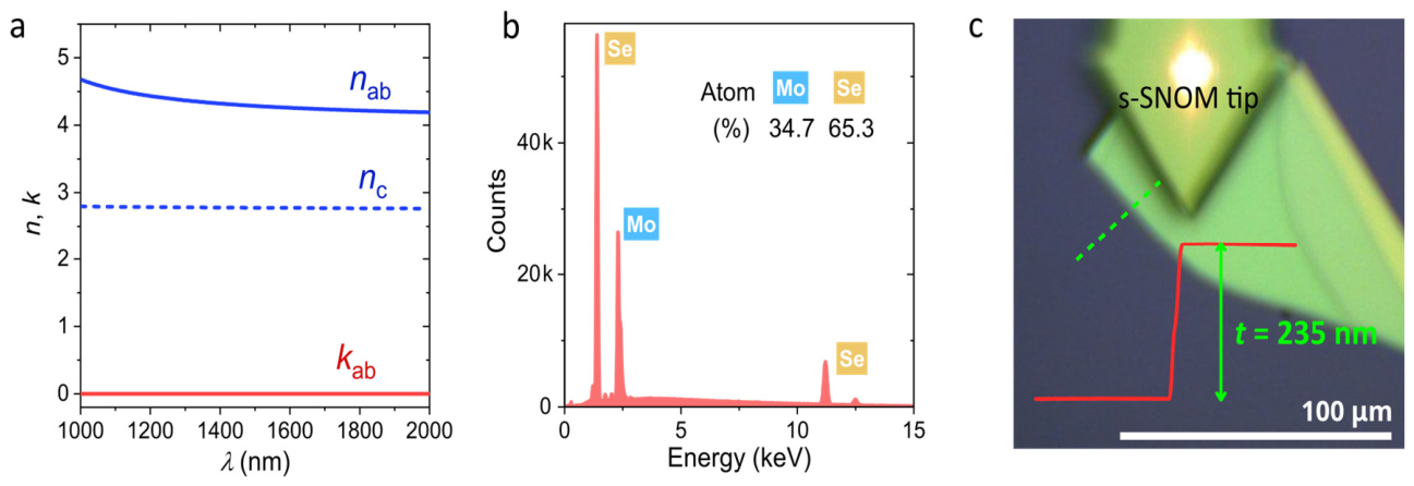
Figure 2.
Near-field characterization of guided modes in MoSe2 planar waveguide. (a) s-SNOM amplitude and phase images acquired near the flake edge at excitation wavelengths of 1475 and 1625 nm, together with representative line profiles. (b) Amplitude of the real part of the complex Fourier-transform spectrum of the signals from (a) at 1475 nm and 1625 nm (frequency normalized to the effective index q/k0 = ns-SNOM). (c) Experimental dispersion points of the planar TM0 mode (blue dots) compared with transfer-matrix calculations (solid orange line) based on the anisotropic optical constants from Figure 1a.
Figure 2.
Near-field characterization of guided modes in MoSe2 planar waveguide. (a) s-SNOM amplitude and phase images acquired near the flake edge at excitation wavelengths of 1475 and 1625 nm, together with representative line profiles. (b) Amplitude of the real part of the complex Fourier-transform spectrum of the signals from (a) at 1475 nm and 1625 nm (frequency normalized to the effective index q/k0 = ns-SNOM). (c) Experimental dispersion points of the planar TM0 mode (blue dots) compared with transfer-matrix calculations (solid orange line) based on the anisotropic optical constants from Figure 1a.
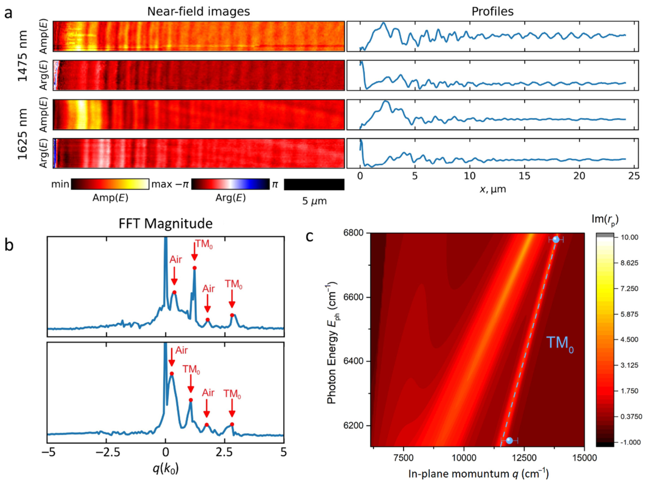
Figure 3.
Effective-index maps for the fundamental waveguide mode of rectangular waveguides with MoSe2 and WS2 cores on a SiO2 substrate as a function of core width and height. The black, white, and blue lines separate the region where no modes are supported from the regions where one, two, or more modes are supported, respectively. The green cross marks the parameters that provide minimal crosstalk between waveguides whose core centers are separated by a distance d = 1 μm.
Figure 3.
Effective-index maps for the fundamental waveguide mode of rectangular waveguides with MoSe2 and WS2 cores on a SiO2 substrate as a function of core width and height. The black, white, and blue lines separate the region where no modes are supported from the regions where one, two, or more modes are supported, respectively. The green cross marks the parameters that provide minimal crosstalk between waveguides whose core centers are separated by a distance d = 1 μm.
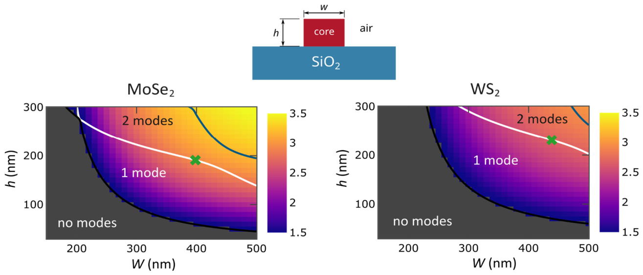
Figure 4.
Coupling length Lc of the fundamental mode as a function of the center-to-center distance d between two parallel waveguide cores. For each value of d, the core dimensions were optimized within the single-mode regime. The inset shows the coupled-waveguide geometry used in the calculations.
Figure 4.
Coupling length Lc of the fundamental mode as a function of the center-to-center distance d between two parallel waveguide cores. For each value of d, the core dimensions were optimized within the single-mode regime. The inset shows the coupled-waveguide geometry used in the calculations.
Disclaimer/Publisher’s Note: The statements, opinions and data contained in all publications are solely those of the individual author(s) and contributor(s) and not of MDPI and/or the editor(s). MDPI and/or the editor(s) disclaim responsibility for any injury to people or property resulting from any ideas, methods, instructions or products referred to in the content. |
© 2026 by the authors. Licensee MDPI, Basel, Switzerland. This article is an open access article distributed under the terms and conditions of the Creative Commons Attribution (CC BY) license (http://creativecommons.org/licenses/by/4.0/).
Copyright: This open access article is published under a Creative Commons CC BY 4.0 license, which permit the free download, distribution, and reuse, provided that the author and preprint are cited in any reuse.


