Submitted:
25 April 2026
Posted:
27 April 2026
You are already at the latest version
Abstract
This work demonstrated improvements in the photovoltaic performance metrics of a dye-sensitized solar cell (DSSC) through the application of Eu-doped strontium silicate – Sr2SiO4:Eu3+, luminescent downshifting (LDS) material. The material converted underuti-lized high energy ultraviolet (UV) photon into lower energy visible photon for better spec-tral responsivity in the DSSC. The LDS material was prepared by the conventional solid state technique. Surface morphology was examined by scanning electron microscope (SEM). Photoluminescence (PL) measurement was applied for the fluorescence emission. The photovoltaic performances of the bare and LDS enhanced devices were analyzed from the photovoltaic current – voltage measurement. Compared to the bare DSSC, the cell with Sr2SiO4:Eu3+ LDS phosphor material had an enhancement of 14.8 % in the short circuit current density (Jsc), from 0.243 – 0.279 mA/cm2. The open circuit voltage (Voc) yielded an improvement of 10 % from 580 – 638 mV. Maximum power output (Pmax) produced a boost of 26.5 % from 0.0136 – 0.0172 mW and the efficiency improvement at 26.6 % from 1.09 – 1.38 %. The coefficient of variation was introduced to evaluate device reproducibility. The device with the incorporation of Sr2SiO4:Eu3+ LDS phosphor, depicted a coefficient of variation of 8.5 %, suggesting good DSSC reproducibility consistency.
Keywords:
short circuit current density
; open circuit voltage
; maximum power output
; luminescent downshifting
; dye-sensitized solar cell
1. Introduction
As the research for clean and environmental friendly energy continues to progress, the solar energy has gained significant attention due to its abundance, sustainable and renewable energy source [1,2,3,4]. Dye-sensitized solar cells (DSSCs) have equally attracted substantial research interest among different solar cell technologies due to their environmental friendliness, cost effectiveness and good performance under diffused light [5,6,7]. Many research works have been published on the DSSCs since the first report by O’Regan and Grätzel [8,9]. On the other hand, DSSCs have a limitation such as low absorption capacity in the ultraviolet (UV) region of the solar spectrum [10,11,12,13]. This is due to low spectral responsivity of the DSSCs in the UV-blue wavelength band. The sensitizer dyes such as N719 and N3 used in the development of the DSSCs mainly absorb within the visible region of the solar spectrum, which leads to underutilization of the incident light. A lot of metal compound dyes have been produced, but even the best of them (N719, N749 and YD2-o-C8) only absorb visible light in the wavelength range of 400 – 700 nm [14,15,16]. In an ideal scenario, the sensitizers should absorb across a broad range of the solar spectrum which includes the UV region, to yield the greatest number of photons. This couldn’t happen, therefore one of the efficient ways to enhance photon absorption is to widen absorption range of the DSSC’s sensitizer dyes – here calls for augmentation with the so-called luminescent materials.
Previous literature by the authors [17] analyzed different luminescent materials for DSSC enhancements, focusing on the mechanism, material types and integration approaches used to improve the photovoltaic performance. The published review identified three major categories of luminescent materials used in DSSC research which were down-conversion, quantum dots and up-conversion. These materials have collectively attracted significant research interest, with bibliometric analysis indicating over 200, 0000 publications in the past decade, inspecting their applications in photovoltaic technology, as depicted in Figure 1. Literature reported by Mayavan [18] reviewed applications of down-conversion/downshifting phosphors for solar cells. It was observed that down-shifting silicate phosphors were employed in solar cells to capture and enhance device performance. Remarkably, silicate based down-converting phosphors enhance solar sensitization in DSSCs, light scattering, anti-reflectivity and stability in solar devices. The review highlighted different energy transfer mechanisms applied in silicate phosphors and addressed different interesting approaches for developing innovative silicate materials for the enhancement of solar cell performance. Study by Luo et al. [19] highlighted an efficient spray pyrolysis-assisted gas-phase aerosol method to prepare CaAl2O4:Eu2+, Nd3+ phosphor particles. They doped the CaAl2O4 matrix particles with Eu2+ and Nd3+ after an additional H2 reduction step. With the prominent emission peak observed at a wavelength of around 440 nm, it was discovered through luminescent emission spectrum measurement that the CaAl2O4:Eu2+, Nd3+ phosphor particles created in the study played a crucial role in down-converting the UV radiation into visible blue light. Using DSSC photo-electrodes, they created TiO2 pastes with different phosphor fractions to study the impact of the CaAl2O4:Eu2+, Nd3+ phosphors on photovoltaic performance. With an increase in the CaAl2O4:Eu2+, Nd3+ particle contents (≤5 wt %) in the TiO2 matrix, they observed that the and power conversion efficiency (PCE) of the DSSCs increased. By adding 5 wt% of CaAl2O4:Eu2+, Nd3+ phosphors material to the TiO2 matrix, the PCE increased to 6.61%. Other literatures demonstrating the application of luminescent phosphor materials in DSSCs are depicted in Table 1 in terms of their corresponding photovoltaic performances.
Luminescent materials exhibit characteristics known as down-shifting of UV or high energy photons, and therefore, luminescent downshifting has the ability to convert high energy photons below 400 nm to lower energy photons above 450 nm. It provides an effective method that involves incorporating luminescent species to the photo-anode of the DSSC device to absorb light of short wavelengths and re-emitting it at longer wavelengths [14,20]. This reduces UV-induced degradation and enhances the spectrum match between incident light and the dye’s absorption profile. Rare earth materials are typically used as LDS materials. They possess strong emission characteristics and LDS using phosphors doped with rare earth materials to enhance DSSCs performances have equally attracted significant research attention in recent times [21,22,23,24]. Main limitation of the DSSCs remains the low spectral response to UV light, of which LDS materials can address. Therefore, our research focuses on synthesis and integration of the LDS material to enhance the absorption profile of the DSSCs. An LDS material such as Strontium silicate doped with europium (III) ions (Sr2SiO4:Eu3+) has good absorption in the UV region and strong emission characteristics in the visible region of the solar spectrum. The host lattice – Sr2SiO4 provides robust and stable incorporation of Eu3+ ions that necessitates efficient emission [25,26,27,28]. Therefore, Sr2SiO4 is a suitable host lattice for LDS application and it is usually synthesized by solid-state reaction technique. The Sr2SiO4:Eu3+ is particularly suitable for LDS due to its high UV absorption, enabling efficient spectral response of light in the short wavelength region. The absorption profile of the N719 sensitizer dye matches well with the emission spectrum of the Sr2SiO4:Eu3+ making it also a suitable spectral converting LDS material for DSSCs.
In this work, we synthesized Sr2SiO4:Eu3+ LDS material and incorporated it to the photo-anode of the DSSC to enhance performance of the device. The material was synthesized using the solid-state reaction technique. The surface coverage was examined by the scanning electron microscope (SEM). Chemical composition of the Eu-doped silicate LDS material was analyzed by the energy dispersive spectroscopy (EDS). The crystal structure and space group was analyzed via X-ray diffraction (XRD) technique. UV-vis-NIR spectroscopy at room temperature was used to evaluate reflectance for optical band gap estimation. Vibrational modes and structural stability were studied by the Raman spectroscopy. Emission profile of the LDS material was analyzed by the Photoluminescence (PL) spectroscopy at room temperature. PL analysis showed sharp emission peaks attributed to 4f – 4f transition of Eu3+ ions, within the visible red-orange spectral region, which aligned favorably with the absorption profile of the N719 dye. Further, we characterized and compared the enhancements in photovoltaic performance of DSSCs with and without the LDS particles incorporation, from the photovoltaic current – voltage (I – V) characteristics. Compared to the bare DSSC, the cell with the integration of Sr2SiO4:Eu3+ LDS phosphor particles had an enhancement of 14.8% in the short circuit current density (Jsc), from 0.243 mA/cm2 to 0.279 mA/cm2. The open circuit voltage (Voc) yielded an improvement of 10% from 580 mV to 638 mV. Maximum power output (Pmax) produced a boost of 26.5% from 0.0136 mW to 0.0172 mW and the efficiency improvement was at 26.6% from 1.09% to 1.38%. Therefore, the novelty of this work is the incorporation of Sr2SiO4:Eu3+ LDS material to enhance the performance of a bare DSSC, which to the best of our knowledge has not been reported.”

Table 1.
Photovoltaic performance parameters of luminescent phosphor materials applied in DSSCs.
| Luminescent phosphor materials | Voc (mV) | Jsc (mA/cm2) | FF (%) | η (%) | Reference |
| SrAl2O4:Eu3+ | 777 | 15.68 | 58.78 | 7.16 | [29] |
| Y3Al5O12:Ce3+ | 780 | 14.5 | 74 | 8.88 | [30] |
| Y2WO6: Eu3+ | 757 | 12.3 | 43 | 3.9 | [31] |
| Y2O3:Eu3+, Gd3+ | 766 | 13.33 | 62.4 | 6.37 | [32] |
| (Sr, Ba, Eu)2SiO4 | 830 | 10.23 | 70.6 | 5.97 | [33] |
| MgAl2O4:Eu3+ | 642 | 14.8 | 62 | 4.8 | [34] |
| BaSnO3:Sm3+ | 810 | 0.62 | 72 | 0.36 | [35] |
| Sm3+ | 690 | 16.71 | 46 | 5.31 | [36] |
| GdVO4:Dy3+ | 680 | 17.40 | 58 | 6.88 | [37] |
| LiYF4:Er3+/Yb3+ | 660 | 22.16 | 72 | 10.53 | [38] |
2. Materials and Methods
2.1. Experiment
Conventional solid-state reaction technique was applied for the synthesis of the strontium silicate Eu-doped material – Sr(2-x)SiO4:xEu3+, (x = 0.03) due to its effectiveness and suitability in producing thermally stable and highly crystalline luminescent materials. High-purity starting materials, including strontium carbonate (SrCO3), 99.99%, silicon dioxide (SiO2), 99.99%, europium oxide (Eu2O3), 99.99%, and lithium carbonate (Li2CO3), 99.99%, as a charge compensation, all analytically graded from Sigma-Aldrich – Merck Group, Johannesburg, South African division, were used in stoichiometric ratio as starting materials. Synthesis route is depicted in Figure 2. Initially, the powders were accurately weighed in stoichiometric proportions and thoroughly ground in an agate mortar to ensure homogeneity in the mixture, thereby ensuring uniform distribution of all constituent elements. The homogeneous mixture was then transferred into a high-purity alumina crucible to avoid contamination during heating. The crucible was placed in a high-temperature programmable muffle furnace for thermal treatment. Calcination was conducted at 550 °C for 2 hours to promote the decomposition of carbonates and the removal of volatile components, resulting in the formation of intermediate oxides. After cooling and regrinding to further enhance homogeneity and particle contact, the sample was subsequently sintered at 550 0C for 4 hours in air atmosphere to facilitate formation of Sr2SiO4:Eu3+. This two-step heating process ensured improved phase purity, enhanced crystallinity, and strong incorporation of Eu3+ ions into the Sr2SiO4 host lattice.
To evaluate the impact of Sr2SiO4:Eu3+ phosphor material incorporation on the performance of dye-sensitized solar cells (DSSC), the phosphor material was incorporated into the TiO2 photo-anode matrix by doctor blade technique. Figure 3 depicted the developmental process, and a composite mixture of TiO2 and Sr2SiO4:Eu3+ paste was prepared by dispersing 2g of TiO2 and 5 wt % of phosphor particles in approximately 10 mL of ethanol, followed by thorough grinding to ensure homogeneous mixing of constituents. Approximately 2 mL dilute HNO3 was added dropwise under continuous stirring to acidify and stabilize the TiO2 – phosphor composite. The resulting paste was deposited on FTO-coated glass substrate using doctor blade technique [39,40] and then heated at 280 0C in hot plate for 5 hours to improve adhesion and crystallinity. The thickness of the film was about 45 µm. The prepared film was immersed in a 0.3 mM solution of N719 dye for 24 hours at room temperature to ensure adequate dye loading on the TiO2 surface. The sensitized photo-anode was then assembled into DSSC device by sandwiching with a platinum-coated FTO counter electrode. For comparative analysis, a bare DSSC device without the Sr2SiO4:Eu3+ phosphor particles, but with a similar thickness (approximately 45 µm) was fabricated and evaluated likewise under same conditions. Thereafter, an iodide/triiodide-based redox electrolyte was subsequently introduced dropwise into the inter-electrode space to complete the cell assembly. The photovoltaic performance of the fabricated DSSCs was evaluated under an indoor light condition with an intensity of approximately 5.0 mW/cm2 detected using the Solar Power Meter instrument. A Keithley 2440 Source Meter was used to record the current – voltage (I-V) characteristics. Key performance parameters such as short circuit current density (Jsc), open-circuit voltage (Voc), fill factor (FF), maximum power (Pmax) and power conversion efficiency (PCE), were also extracted and compared between the phosphor-doped and bare devices.”
“DSSCs consist of several key components such as photo-anode, dye sensitizer, electrolyte, and counter electrode. The photo-anode is composed of fluorine-doped tin oxide (FTO), coated with a mesoporous semiconductor layer, such as titanium dioxide (TiO2), which provides a sufficient surface area for the dye molecules to be adsorbed. The operation of DSSCs relies on a series of electrochemical processes that collectively convert light into electricity [41,42], as shown in Figure 4. At the top is a transparent conductive layer, which allows sunlight to enter while also serving as an electrode. Beneath it lies a mesoporous layer of TiO2 nanoparticles coated with dye (sensitizer) molecules. This structure is critical because the TiO2 provides a large surface area for dye adsorption, maximizing light absorption even though TiO2 itself is not an efficient visible-light absorber, the dye molecule is. The integration of phosphors particles provides down-shifting effect mechanism, where UV light is absorbed sufficiently and emitted at the visible light wavelengths for better utilization in DSSC. When sunlight strikes the cell, photons are absorbed by the dye molecules, exciting electrons from their ground state to a higher energy level. These excited electrons are then injected into the conduction band of the TiO2. The diagram’s arrow shows this electron flow into the semiconductor network, from where electrons travel through the interconnected TiO2 particles to the FTO electrode [43]. From there, they move through the external circuit, generating electrical work before reaching the counter electrode at the bottom.
2.2. Optical Band Gap Estimation
Optical band gap entails the minimum photon energy required to promote an electron from the valence band to the conduction band, which can be determined from the reflectance or absorbance spectrums [44,45]. From the Planck-Einstein relation, we recall that photon energy (E) is related to the photon wavelength (λ) by:
where h and c are Planck’s constant (4.136 x 10⁻¹⁵ eV.s) and speed of light (3 x 10⁸ m/s). , therefore, increasing photon energy implies decreasing the wavelength. With respect to reflectance (R), normalization is crucial to scale the reflectance data to the [0, 1] range. This is to mitigate amplitude-based effects in derivative analysis in order to realize a unity peak of the reflectance spectrum. Normalization technique applied is depicted as:
In order to highlight rapid changes in reflectance, computation of the first derivative of the normalized reflectance with respect to the photon energy is also vital. This indicates electronic transition from the valence band to the conduction band [46,47]. Since R is a function of the wavelength, we can obtain by:
Relationship between wavelength and photon energy is governed as:
Derivative of the wavelength with respect to photon energy yields.
Substituting Equation (5) into (3) gives
The value where reaches its maximum, entails the bang gap energy which is the energy corresponding to the maximum first derivative. This expression is shown in Equation (7). The derivative-based approach provides a computationally efficient method to estimate optical band gaps from reflectance spectra as a function of wavelength, which represents a useful tool in exploratory material analysis.
2.3. Estimation of Overlap Integral and Förster Distance
In order to facilitate efficient energy transfer there must be a spectral overlap between the emission spectrum of the donor and the absorption spectrum of the acceptor. The overlap integral – is governed below as:
(8)
where is the normalized emission spectrum of the donor which is a dimensionless entity, is the molar absorption or extinction coefficient of the acceptors – a measure of how strongly chemical species absorb light at a particular wavelength in and is the wavelength of the incident light in nm.
The distance between donor and acceptor molecules as well as the strength of the overlap integral determines the efficiency of the energy transfer. Therefore, the smaller the distance between the donor and the acceptor molecules and the larger the overlap integral, the more the efficiency of the energy transfer. A convenient way to express the J-overlap integral is in terms of the Förster distance, which is the distance at which energy transfer efficiency via Förster Resonance Energy Transfer (FRET) – is 50%. The efficiency of energy transfer via FRET can be generally expressed as in Equation (9) [48]. FRET is a non-radiative process through which energy is transferred from the donor (LDS material) to the acceptor (N719 dye molecules) via dipole-dipole interaction.
where is the distance between the donor and the acceptor molecules, is the Förster distance upon which the energy transfer efficiency is 50%. Equation 10 expresses the Förster distance in Angstrom () [48].
is given as 2/3 which represent the relative orientation of the transition dipoles of the donors and acceptors. is the quantum yield of the donor in the absence of the acceptor – in this case a value of 0.88 for silicate doped Eu3+ [49]. The is refractive index of the medium containing the donor and acceptor molecules which is 1.33. is the overlap integral between the donor and acceptor molecules and is a numerical coefficient of value 0.211 . Table 2 shows the computed FRET parameters.
2.4. Modified Scherrer Equation for the Crystallite Size Estimation
The approach usually applied to determine the size of a crystal (L) is the Scherrer equation as shown in Equation 11 [50,51].
where, K, λ, θ, and β are the shape factor (K= 0.9), X-ray wavelength [Cu-Kα (λ=0.15405 nm)], X-ray diffraction angle, and full-width at half maximum (FWHM) in radians, respectively.
Applying the original Scherrer equation directly to estimate the crystallite size of a sample would lead to a lot of systematic errors because sometimes the diffracted peaks of the sample do not yield the same crystallite size result [50]. However, in order to decrease the source of experimental errors and to obtain the average value of the crystallite size from all the peaks or any number of selected peaks, the use of the modified Scherrer equation is vital [50]. The modified Scherrer equation uses the least square regression method to precisely reduce the experimental errors and estimate more accurately the crystallite size of the phosphors. The Scherrer equation can be modified as follows:
A plot of Inβ against In(1/cosθ), would yield a straight line graph with a slope and intercept. Since errors are related with the experimental data, the least square regression method would be applied to obtain the best slope and most accurate In(Kλ/L) as the intercept. The actual value for the crystallite size can then be estimated by taking the exponential of the intercept, and having the known values for K and λ as 0.9 and 0.15405 nm, respectively.
The modified Scherrer equation is very vital and advantageous at decreasing the sum of absolute values of errors, ∑ (±∆Inβ) 2 and producing a line through the data points to extrapolate the intercept.”
2.4. Photovoltaic Performance Calculation
The light to electrical energy conversion efficiency () of the bare DSSC and Sr2SiO4:Eu3+ embedded DSSC were calculated using Equation (15), with the values of short-circuit current density (), open circuit voltage () and the maximum power () taken from the I-V characteristics:
is the intensity of the light and A is active surface area of the DSSC. The fill factor (FF) is defined by Equation (16).
3. Results and Discussion
3.1. SEM Analysis
Scanning Electron Microscope (SEM) of the LDS material is depicted in Figure 5(a). The micrograph revealed microstructural morphology composed of irregular shaped agglomeration of particles of rough and porous coverage. The agglomeration of smaller particles into larger clusters indicates sintering and grain coalescence. The porosity morphology facilitates ionic mobility within the photo-anode, contributing positively to charge separation and transport [52]. Figure 5(b) shows the Landau distribution fit which reveals the particle size distribution (frequency vs. particle size) of Sr2SiO4:Eu3+ phosphor material. The red bars represent the histogram of measured particle sizes, while the blue curve represents a Landau distribution fit to the data. The histogram exhibit a strongly asymmetric right-skewed profile (positive distribution which tails of more on the right side), with the majority of particles falling within the 1-3 µm range and a pronounced maximum centered near 1.5-2.5 µm. This indicates that the thermal treatment promotes the formation of relatively fine particles while still allowing a minor population of larger grains to persist, as evidenced by the extended tail reaching up to approximately 8 µm.
Further, the Landau curve models this asymmetry effectively, capturing both the sharp rise at small sizes and the long decay toward larger values. Such a distribution confirms non-uniform (mixture of small and large particle clusters) grain growth, where most grains remain small but occasional abnormal growth or agglomeration leads to the formation of oversized particles. The mean particle size was estimated to be approximately 2.35 µm, which is small on a micro range. This particle size is essential when evaluating the suitability for DSSC applications as it directly influences the surface area, dye loading, light scattering and electron transport properties [53,54]. A mean particle size of microns places this phosphor material in the micro-scale regime which exhibits reduced surface-defect densities, improved scattering behavior, and favorable packing characteristics, features that can be advantageous for light scattering centers, effectively increasing the optical path length of incident light and thereby enhancing photon absorption by the sensitized dye. This is particularly beneficial in improving the short-circuit current density (Jsc) of the device.
3.2. EDS Analysis
The energy dispersive spectroscopy (EDS) is a technique used to determine and analyze the elemental composition of materials [55], and to confirm the successful incorporation of dopant ions within the host lattice. Figure 6 displayed the measured X-ray counts as a function of the energy level in keV, enabling identification of the characteristic emission peaks associated with each constituent element. In the spectrum, the well-defined peaks corresponding to the characteristic X-ray emission of Strontium (Sr), Silicon (Si), Oxygen (O), and Europium (Eu) were observed, indicating that all expected elements are present in the sample. Sr exhibits the most prominent peak, consistent with its high atomic number and greater X-ray emission efficiency, followed by Si and O. The sample exhibits intense Sr and Si peaks alongside clearly resolved Eu signals, indicating a uniform elemental distribution and effective dopant substitution. The most prominent Sr peaks appeared around 2 keV and 14 keV, while for Si is located around 1.8 keV. Moreover, the Eu peaks are more distributed at approximately 1.2 keV and within the range 5.8 – 7.8 keV. The most notable of these peaks appear around 1.2 keV and 5.8 keV, indicating the presence of Eu3+ in the crystal lattice. This Eu3+ ions are well effectively incorporated into the Sr2SiO4 lattice, likely due to enhanced diffusion and solid-state reaction kinetics during the annealing, leading to improved crystallinity and good structural organization [25]. Consequently, the material achieved well-ordered and good crystalline state, which is beneficial for luminescent performance.
3.3. XRD Analysis
Powder X-ray diffraction (XRD) measurement of the LDS material was performed on a Panalytical Powder diffractometer in the 2theta range from 10 to 800 with monochromatized Cu-Kα radiation (λ = 0.15406 nm). Figure 7 represents the XRD patterns of the Sr2SiO4:Eu3+, with the corresponding international Centre for Diffraction Data (ICDD) card number 01 – 076 – 1630. The diffraction peaks corresponded with one another and are in agreement with the ICDD card number profile, which indicates that the solid state technique applied ensured effective synthesis of the strontium silicate material. Introduction of the activator Eu3+ ions did not significantly alter the crystal structure of the Sr2SiO4, indicating that Eu3+ ions was effectively incorporated into the host lattice. The Sr2SiO4 exhibits a monoclinic structure with space group: P21/n [56,57]. The lattice parameters were determined to be a = 5.663 Å, b = 7.084 Å, c = 9.767 Å, α = β = γ = 90 0, V = 391.39 Å3.
“The monoclinic structure, space group and lattice parameters of Sr2SiO4 were determined by the ICDD pattern using the experimental data. It is pertinent to state that what majorly determines the crystal system (monoclinic or orthorhombic structure) is the space group, not the lattice parameters which can change depending on the synthesis technique. The intensity of the peaks suggests that the material has undergone a complete phase transformation and that the crystal grains have become more ordered. This enhanced crystallinity is advantageous for applications requiring efficient charge transport and stable structural properties, as it minimizes defects and grain boundaries that can act as charge traps or recombination centers. The crystal structural property is expected to translate into better optical and electronic properties, making the material suitable for advanced applications such as light-emitting devices and, potentially, dye-sensitized solar cells (DSSCs).
In order to quantitatively determine the crystallite size of the sample, the modified Scherrer equation remains advantageous at decreasing the sum of absolute values of errors, and developing a line through the data points to extrapolate the intercept [58,59], and can be of great use in determining whether samples are of the same crystallite size. Figure 8 provides the linear regression plots of verses for determining the crystallite size of the material. Table 3 provides the quantitative estimated crystallite size value with the respective standard error sample. The crystallite size was estimated to be 19.5 nm for the LDS material, showing a relatively small crystallite size, however the sample annealed at 650 0C exhibits smaller crystallite size of 14.86 nm with a similar standard error (0.91 nm), suggesting that temperature treatment in this case leads to inhibited crystal growth or enhanced recrystallization processes that produce fine crystallite. Moreover, small crystallite size increases the surface area to volume ratio of the phosphor material, which can enhance the material’s light absorption capacity and equally improve the material’s luminescent efficiency, thereby resulting in better light emission [60]. The behavior of excitons (electron-hole pairs) is also affected by crystallite size. In small crystallites, the increase in the movement and interaction of excitons, potentially leads to more efficient energy transfer and absorption of light, which is crucial in promoting the light absorption capacity and the performance of DSSCs.
3.4. Raman Spectrum
The Raman spectrum reveals insights into the lattice vibrational properties of materials as a function of wavenumber [61,62]. It is particularly essential for analyzing the behaviour of silicate network. From Figure 9, the spectrum displayed the characteristic fingerprint of a silicate lattice: The characteristic peaks associated with Si–O vibrational modes were clearly observed. Many peaks appearing in the spectrum may likely correspond to vibrations of the Si–O bonds, which are key signatures of the tetrahedral SiO4 units that form the basis of the silicate network in Sr2SiO4. These vibrational modes are essential indicators of the connectivity of the silicate tetrahedral. Peaks appearing around 1400–1500 cm−1 may correspond to overtones or non-bridging oxygen atoms. Additionally, bands near 1650–1750 cm−1 are likely associated with the bending modes of molecular water (H–O–H), indicating the possible presence of adsorbed moisture or hydroxyl groups on the material surface. The intense and sharp peak around 2450 cm−1, could be due to second-order Raman scattering or combination modes involving Si–O vibrations, which becomes more prominent as the material becomes more crystalline. The presence of weak broad bands around 2600–3000 cm−1 and the broad O–H stretching mode near 3600 cm−1 further support the likelihood of residual hydroxyl groups or surface-bound moisture. In this spectrum, there is no strong indication of the distinct Eu–O vibrational modes, suggesting that Eu3+ ions are well incorporated into the lattice without significantly altering the dominance Si–O network vibrations.
3.5. Diffused Reflectance
Diffused reflectance spectrum of the samples are shown in Figure 10. The material exhibits strong reflectance between 410 and 800 nm, corresponding to the visible and near-infrared regions, while a marked decline in reflectance occurs below 400 nm, within the ultraviolet (UV) range. This decline indicates efficient absorption of UV photons, a behaviour linked to the material’s luminescent downshifting ability – specifically, its capacity to absorb high-energy UV light and re-emit it as visible light. This process is facilitated by electronic transitions from the f – f energy levels of Eu3+ ions. Given its strong UV absorption, Sr2SiO4:Eu3+ has potential as a UV-harvesting material in optoelectronic systems, such as dye-sensitized solar cells (DSSCs), where it can convert unused UV radiation into usable visible light, thereby improving power conversion efficiency.
The sample’s reflectivity started at lower (~55%) and increases more modestly to ~78–82% in the visible region. In the visible range of the solar spectrum, this material reflected substantial amount of light – unlike conventional sensitizing dyes such as N719 and various organic dyes, which are designed to absorb visible light efficiently. As a result, Sr2SiO4:Eu3+ is not suitable for use as a surface coating, since its high reflectivity in the visible spectrum would interfere with light absorption. Instead, it is more effective when integrated within the device architecture, such as in an internal or interfacial layer, where it can selectively absorb UV light without disrupting visible light transmission. While it is not meant to replace traditional dye molecules, it can serve as a complementary sensitizer, extending the device’s absorption capacity into the UV region and aiding in the generation and transport of photo-induced charge carriers.
To further study the optical properties of the annealed Sr1.97SiO4:0.03Eu3+ phosphor samples, we have estimated the optical band gap from the first derivative of the diffuse reflectance spectrums as shown in Figure 11. We have located the absorption edge with respect to photon energy . The prominent peak observed corresponds to the energy at which photon absorption initiates electronic transitions from the valence band to the conduction band. The x-axis value (photon energy) where this peak intersects indicates the band gap energy. For Sr2SiO4:Eu3+ LDS material, this intersection occurred near 3.36 eV; suggesting direct band gaps that fall within the ultraviolet (UV) portion of the electromagnetic spectrum [63].
In the context of dye-sensitized solar cells (DSSCs), this band gap implies that Sr2SiO4:Eu3+ is not suitable as the main light-absorbing material or as a photo-anode, since it does not significantly absorb visible light—the most intense part of the solar spectrum. However, its strong absorption in the UV range makes it highly suitable as a luminescent downshifting material. As previously discussed alongside the material’s reflectance behaviour, Sr2SiO4:Eu3+ can efficiently capture UV photons and re-emit them in the visible range through the characteristic sharp emission peaks, corresponding to the transition from the excited state 5D0 to the ground states 7Fj (j =0, 1, 2, 3 and 4) in the 4f6 configuration of the Eu3+ ions. This re-emitted visible light can subsequently be absorbed by common sensitizer dyes used in DSSCs, such as N719 (ruthenium-based) and various organic dyes, which operate effectively in the 400–700 nm range [64,65,66]. Thus, these band gaps confirm Sr2SiO4:Eu3+’s potential as a spectral conversion material. While not contributing directly to visible light absorption, it enhances solar cell efficiency indirectly by transforming non-utilized UV light into a form that dye molecules can absorb. Additionally, it offers the added benefit of shielding the device from UV-induced damage, contributing to the longevity and overall performance of the DSSC.
3.6. Photoluminescence Analysis
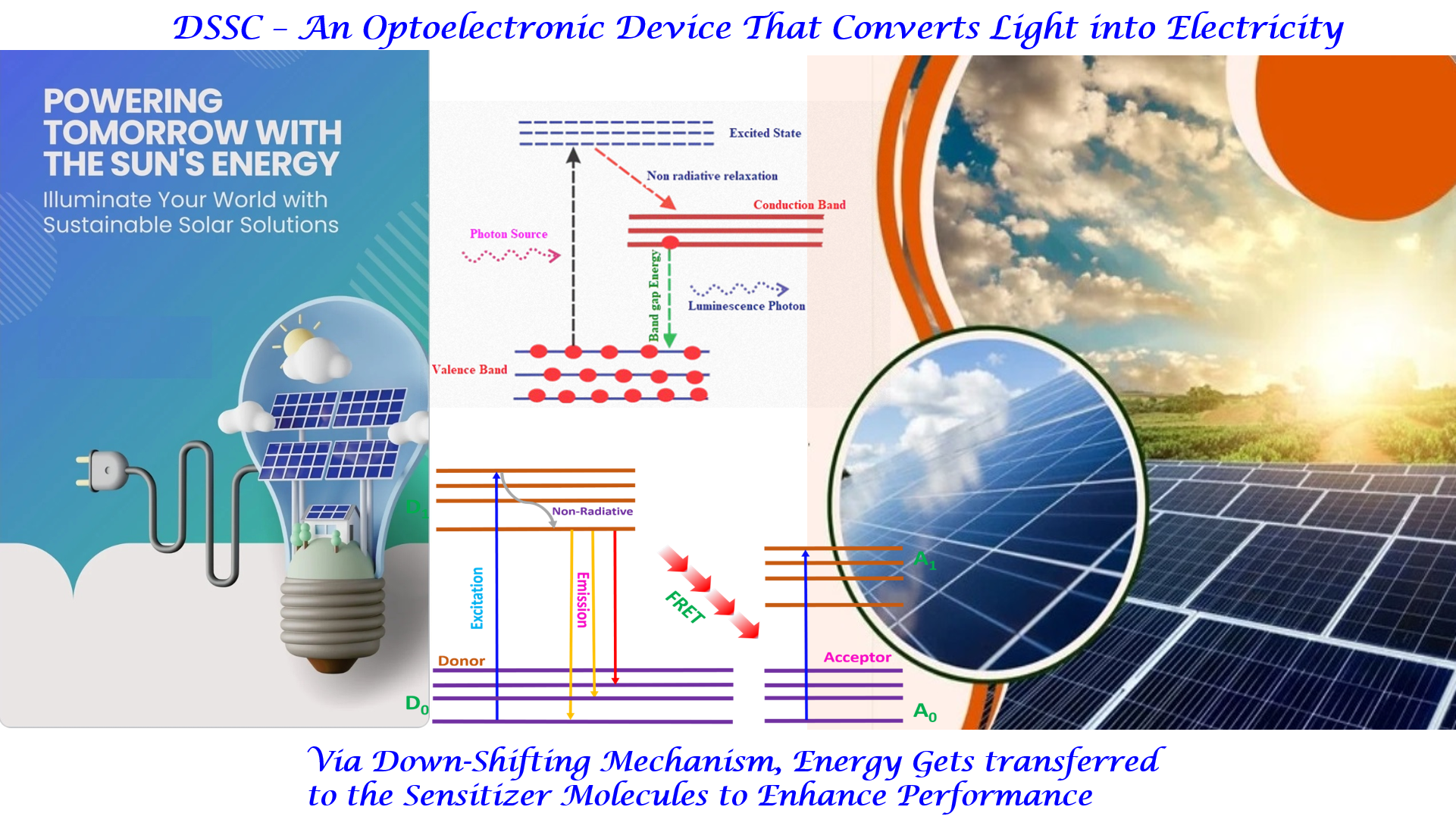
In typical photo-luminescent process, light of suitable energy is directed onto a sample material, where it is absorbed, exciting electrons from valence band to higher energy excited state, a process known as photo-excitation. When the excited electrons subsequently relax back to ground energy states, they emit energy in a process known as PL photoluminescence [67]. Therefore, PL is essentially the spontaneous emission of light from a material under optical excitation [68]. The light emitted can be collected and analyzed spectroscopically to obtain valuable information about the material’s electronic structure, bandgap energy, defect states, and recombination mechanisms. Moreover, the intensity and wavelength distribution of the PL signal provide insights into the purity, crystallinity, and defect density of the material. A material under photo-excitation will have its electrons moved from the valence band to the allowed excited states, creating electron hole pairs called excitons. As these electrons and holes recombine, the system may release energy, which may include emission of light (luminescence/radiative process) or may not (non-radiative process, where the energy is dissipated as heat through phonon interactions), as demonstrated in Figure 12. The energy of the emitted light i.e., PL relates to the band gap energy between the excited and the equilibrium states. In semiconductor devices, the most common radiative transition occurs between the conduction and the valence band of the material, and their energy difference is known as the band gap. During PL spectroscopy experiment, excitation is provided by a light source with the energy that is larger than the semiconductor material’s band gap. The photo-excited carriers are the electrons and holes, which relax within their respective band edges and recombines by emitting light known as a luminescence photon.
The Sr2SiO4:Eu3+ is a promising material due to its sharp and intense luminescence characteristics 4f – 4f transition. Among rare-earth-doped phosphors, Eu3+ is particularly attractive for applications that demand tunable emission and thermal stability [26]. These features make Sr2SiO4:Eu3+ not only suitable for solid-state lighting and display technologies, but also relevant in the context of energy conversion devices, such as dye-sensitized solar cells. From Figure 13, the PL emission spectrum of the sample spanned in the wavelength range of approximately 350 – 800 nm which illustrates the characteristic luminescence response of the Eu3+ and are dominated by sharp and intense luminescence, originating from characteristic 4f – 4f transitions, which are parity-forbidden but become allowed due to the asymmetric ligand field around Eu3+ ions. Several distinct emission bands were observed, predominantly in the UV and near infra-red spectral region. These bands are attributed to the well-known 5D0 → 7FJ (J = 0–4) transitions of Eu3+ ions [69]. Among them, the most intense emission appears in the infrared region around 612–620 nm, which is associated with the electric dipole transition 5D0 → 7F2 emanating from the local symmetry of the Eu3+ sites. This transition is highly sensitive to the local crystal field and is a hallmark of Eu3+ occupying sites lacking inversion symmetry within the host lattice, with higher intensity indicating a more distorted or non-centrosymmetric environment.
In conventional DSSCs, the performance is limited by the spectral response of the dye molecules, which often absorb inefficiently in the UV region. Phosphors such as Sr2SiO4:Eu3+ can be strategically applied as spectral converters or luminescent down-shifting layers. When integrated into the photo-anode architecture or applied as a top layer, these materials can absorb high-energy UV or blue photons and re-emit them in the visible and near infra-red spectral range, which matches better with the absorption profile of typical dyes such as N719 or organic D-π-A molecules. This re-emission can then be absorbed by the dye, effectively increasing the number of photons available for charge generation and improving the overall photocurrent [70].
Among the various dyes developed for DSSCs, the N719 dye has become a standard due to its broad absorption in the visible range, good chemical stability, and favorable alignment of energy levels for electron injection and regeneration [71]. One major limitation in DSSC performance arises from the mismatch between the solar spectrum and the dye’s absorption characteristics. In particular, UV photons below 350 nm are poorly utilized by many DSSC dyes, including N719, either due to low absorption or inefficient electron injection. Moreover, prolonged UV exposure can cause photo-degradation of the dye or the electrolyte, limiting the long-term stability of the device. A promising strategy to address these challenges involves the use of luminescent materials such as phosphors that can absorb high-energy UV photons and re-emit them in the visible range where the dye has strong absorption [17]. This approach, referred to as spectral down-conversion or luminescent down-shifting, has potential not only to increase the number of useful photons incident on the dye but also to shield sensitive components from harmful UV radiation. Figure 14 shows that comparing N719 dye absorption and the Sr2SiO4:Eu3+ emission revealed that the N719 dye showed strong absorbance between 350 – 600 nm. While the absorbance significantly decreased beyond 600 nm.
This is particularly relevant because Sr2SiO4:Eu3+ emits strongly at approximately 612 nm, meaning that photons emitted by the phosphor at this wavelength can still be absorbed by the N719 dye. This overlap, although not ideal, is sufficient to propose the use of Sr2SiO4:Eu3+ as a spectral converter in DSSCs utilizing N719 [72]. When UV photons (e.g., < 350 nm) that are otherwise under-utilized are absorbed by the phosphor, the resultant visible emission can contribute to enhanced light harvesting if those emitted photons fall within the dye’s absorptive window. The degree of spectral overlap between the phosphor’s emission and the dye’s absorption is a key factor in determining the effectiveness of the down-shifting process [72,73]. FRET spectral integral between the emission spectrum of Sr2SiO4:Eu3+ and the absorption spectrum of the N719 dye molecules showed that strong overlap was achieved between the phosphor material and the dye molecules, and an estimated spectral overlap integral J(λ) value of 5.91 x 10¹⁰ M-1cm-1nm4 was realized from the material. This value is sufficient enough, indicating an efficient energy transfer process could occur [48,74]. The overlap strength realized is appropriate as it depicted proper correspondence between the absorption spectrum of the N719 dye acceptor and the emission spectrum of the Sr2SiO4:Eu3+ donor.
FRET efficiency as a function of distance between the donor and the acceptor molecules is depicted as shown in Figure 15 below. It can be deduced that the FRET efficiency decreases as the distance between the donor and the acceptor increases, which demonstrates that FRET is always effective at a typically close distance. R0 = 9.96 nm indicated the participation of FRET mechanisms, which fall within the range 1–10 nm. Therefore, at such distances, the energy transfer between the donor, Sr2SiO4:Eu3+, and the acceptor, the N719 dye, would be 50% efficient. Estimation of R0 was computed from the relationship governing the Förster distance, the quantum yield of the donor in the absence of the acceptor, the spectra overlap between the donor and acceptor molecules, the refractive index of the medium containing the donor and the acceptor molecules, and the relative orientation of the transition dipoles of the donor and acceptor.
Generally, the development of an efficient energy transfer system is strongly dependent on the Förster distance between the donor and acceptor molecules as well as the strength of the spectra overlap integral between the donor and acceptor. A system with a Förster distance between 1 – 10 nm and a strong overlap between the donor and the acceptor molecules would produce efficient energy transfer [14,75]. This mechanism in DSSC would facilitate generation of charge carriers that would promote the power output and the overall performance of the device.
3.7. Energy Level Diagram
The diagram in Figure 16 illustrates how Sr2SiO4:Eu3+ is integrated into a dye-sensitized solar cell (DSSC) to enhance light harvesting and charge transfer. At the top, the Eu3+ luminescent centers show a typical photo-physical process: incident high-energy photons excite electrons from the ground state to an excited state (blue upward arrow). After excitation, part of the energy is lost through a non-radiative transition, followed by radiative emission (green downward arrow). This emission corresponds to visible light, meaning the phosphor acts as a down-shifting layer, converting higher-energy UV photons into wavelengths better matched to the dye absorption. The emitted light from Sr2SiO4:Eu3+ is then reabsorbed by the sensitizer, here N719 dye. In the diagram, the dye’s HOMO–LUMO levels are clearly positioned between the conduction band of TiO2 and the redox electrolyte. Upon photon absorption (either direct sunlight or re-emitted light from Eu3+), electrons in the dye are excited from the HOMO to the LUMO. Because the LUMO lies above the TiO2 conduction band edge, the excited electrons are efficiently injected into TiO2, which is essential for photocurrent generation [76]. Once injected, electrons percolate through the TiO2 network and are collected by the transparent conducting electrode, typically FTO. The energy alignment shown indicates that TiO2 has a slightly higher (less negative) conduction band than FTO, allowing downhill electron transport. The diagram’s arrows emphasize this directional flow toward the external circuit, minimizing recombination losses when the interfaces are well optimized. Meanwhile, the oxidized dye is regenerated by the electrolyte, commonly the, I−/ I3− redox couple. The redox potential is positioned above the dye HOMO, enabling electron donation to the dye. This regeneration step is critical to sustain continuous operation. The cyclic red arrows in the diagram represent the oxidation of iodide (I− → I3−) at the dye interface and its subsequent reduction at the counter electrode. At the counter electrode, typically coated with Platinum, the tri-iodide (I3−) is reduced back to iodide by electrons returning from the external circuit. This closes the electrochemical loop. The energy level of Pt facilitates fast charge transfer kinetics, reducing over-potential and improving fill factor. Overall, the inclusion of Sr2SiO4:Eu3+ introduces a spectral conversion mechanism that broadens the usable portion of the solar spectrum. By converting UV photons (which are poorly absorbed by N719 dye) into visible emission, it enhances photon utilization. The diagram also highlights that efficient DSSC operation depends on precise energy level alignment: dye LUMO above TiO2 conduction band for injection, dye HOMO below electrolyte redox potential for regeneration, and seamless electron transport through FTO and Pt.
3.8. Photovoltaic Performance Analysis
Measurement of the current density (J) – voltage (V) characteristics of solar cells is vital to determine the overall performance of the cells. The power – voltage characteristics can also be determined, as power is proportional to the product of current and the voltage. From the J – V and P – V characteristics, a comprehensive set of important photovoltaic parameters can be determined, providing critical insight into the electrical behaviour and overall energy-conversion capability of the device [77,78,79]. These curves enable the determination of key performance indicators, including the short-circuit current density (Jsc), open-circuit voltage (Voc), maximum power output (Pmax), fill factor (FF), and power conversion efficiency (PCE), which collectively reflect the charge-generation efficiency, recombination dynamics, and operational stability of the solar cell. Figure 17(a) illustrates the current density – voltage (J – V), characteristics of a bare dye-sensitized solar cell (DSSC) without the incorporation of any luminescent material, while Figure 17(b) shows the corresponding power–voltage (P–V) characteristics. As the applied voltage increased from 0 to approximately 600 mV, the current density decreased steadily from approximately 0.25 mA/cm2 to nearly zero, demonstrating the expected non-linear relationship between current and voltage in a photovoltaic device [80]. The high current density at low voltage corresponds to the short-circuit current-density region, whereas the decreased current density at higher voltage reflected the approach toward the open-circuit voltage (Voc). On the other hand, the power output initially increased with voltage, reached a maximum around 300-350 mV, and then declined sharply as the device approached Voc. This bell-shaped curve is characteristic of DSSC performance, with the peak representing the maximum power point (MPP), the operating condition under which the device produces its highest electrical power output.
The integration of Sr2SiO4:Eu3+ phosphor, annealed at 550 °C into the DSSC structure has led to a clear enhancement in device performance when compared to the bare cell. The current density–voltage (J – V) and power–voltage (P – V) characteristics are shown in Figure 18 (a & b). Similarly to the bare, the J-V curve exhibits a progressively decreasing current density as the applied voltage approaches the open-circuit region, which is still expected of dye-sensitized solar cells [81]. Compared with the bare cell, the short-circuit current density (Jsc) increased from 0.243 mA/cm2 in the bare DSSC to 0.279 mA/cm2 in the phosphor-modified Sr2SiO4:Eu3+ device, denoting an increase of around 14.8%. This improvement indicates that the phosphor material enhances photon harvesting and light-conversion efficiency, most likely through its down-conversion or spectral-conversion capability. By converting high-energy UV photons into visible wavelengths that align with the N719 dye’s absorption range, more electrons are injected into the TiO2 conduction band, resulting in a higher photocurrent. The curve shape remains smooth and consistent, suggesting that the phosphor layer does not introduce significant recombination pathways or series resistance losses within the cell. Figure 18 (b) shows the corresponding power–voltage (P–V) characteristics for the LDS incorporated device. The power output increases with voltage until reaching a maximum at the device’s maximum power point (MPP), located around 350–400 mV with a peak power of approximately 0.017–0.018 mW. This peak value is higher than that observed for the bare DSSC, further confirming that the incorporation of Sr2SiO4:Eu3+ LDS material contributes positively to cell performance. The improved MPP signifies more efficient harvesting and utilization of the incident solar irradiance. The nearly symmetrical rise and fall of the P–V curve reflected stable and predictable device behaviour, indicating that the phosphor material integrates well with the photo-anode without creating interfacial instability or optical loss. Collectively, these results demonstrated that adding Sr2SiO4:Eu3+ LDS material enhanced both photocurrent generation and power output, confirming its effectiveness as a luminescent down-shifting material for boosting DSSC efficiency.”
The summary of the photovoltaic performance of the bare and the phosphor enhanced devices are depicted in Table 4. The bare DSSC has the following photovoltaic performance parameters: Jsc = 0.243 mA/cm2, Voc = 580 mV, Pmax = 0.0136 mW, FF = 38.60% and PCE = 1.09%. The DSSC with Sr2SiO4:Eu3+ LDS material has the following performance parameters: Jsc = 0.279 mA/cm2, Voc = 638 mV, Pmax = 0.0172 mW, FF = 38.65%, and PCE = 1.38%. Compared to the bare DSSC, the cell with Sr2SiO4:Eu3+ LDS material had an enhancement of 14.8% in the short circuit current density (Jsc), from 0.243 mA/cm2 to 0.279 mA/cm2. The open circuit voltage (Voc) yielded an improvement of 10% from 580 mV to 638 mV. Maximum power output (Pmax) produced a boost of 26.5% from 0.0136 mW to 0.0172 mW. Fill factor yielded an improvement of 0.1% from 38.60% to 38.65%. The efficiency improvement was at 26.6% from 1.09% to 1.38%.
To enable direct comparison, the current density – voltage curves and the power – voltage curves of the bare and phosphor modified cells were plotted on the same axis as shown in Figure 19(a & b). The baseline device exhibited relatively low photovoltaic performance, with a short-circuit current density of 0.243 mA cm−2 and maximum power output of 0.0136 mW, leading to a power conversion efficiency of 1.09%. The relatively low values likely reflected inherent limitations in light harvesting and spectral mismatch between the incident solar spectrum and the absorption range of the dye sensitizers. Upon incorporation of Sr2SiO4:Eu3+ phosphor annealed at 550 °C, improvements were observed across all photovoltaic parameters. The short-circuit current density increased from 0.243 mA cm−2 to 0.279 mA cm−2. The maximum power output improved from 0.0136 mW to 0.0172 mW (26.5% increase), resulting in a corresponding increase in power conversion efficiency from 1.09% to 1.38%, representing a 26.6% improvement relative to the bare device.”
To evaluate the reliability and reproducibility of the fabricated dye-sensitized solar cells (DSSCs), a statistical analysis was conducted using the photovoltaic parameters obtained from reproduced measurements of the J–V and P–V curves. The key parameters considered in this analysis were the short-circuit current density (Jsc), open-circuit voltage (Voc), maximum output power (Pmax), and power conversion efficiency (PCE). These parameters were extracted from the J-V and P-V characteristics measurements for two bare DSSCs and two modified DSSCs incorporating Sr2SiO4:Eu3+ (SSO: Eu3+) phosphor, which are depicted in Figure 20 (a & b). The purpose of this analysis was to assess the reproducibility of device performance and to determine how the incorporation of the luminescent material influences the overall photovoltaic behavior.
Table 5.
Summary of reproduced photovoltaic parameters.
| Device Type | Device ID | Jsc (mA/cm2) | Voc (V) | Pmax (mW) | PCE (%) |
| Bare Cell - 1 | B1 | 0.207 | 0.464 | 0.0120 | 0.96 |
| Bare Cell – 2 | B2 | 0.243 | 0.580 | 0.0136 | 1.09 |
| Modified (SSO: Eu3+) - 1 | M1 | 0.266 | 0.574 | 0.0153 | 1.22 |
| Modified (SSO: Eu3+) - 2 | M2 | 0.279 | 0.638 | 0.0172 | 1.38 |
To quantitatively evaluate the reproducibility of the photovoltaic parameters, the mean values and standard deviations (SD) [82,83] were calculated for each device category and depicted in Table 6. The bare DSSCs exhibited an average Jsc of 0.225 ± 0.026 mA cm−2 and an average Voc of 0.522 ± 0.082 V. The mean Pmax and PCE values were found to be 0.013 ± 0.001 mW and 1.02 ± 0.09%, respectively. The relatively larger uncertainty observed in Voc for the bare devices suggests that slight variations in fabrication or interface quality may influence the open-circuit voltage. For the DSSCs modified with SSO:Eu3+, the mean Jsc increased to 0.272 ± 0.009 mA cm−2, indicating improved and more consistent photocurrent generation. The average Voc increased to 0.606 ± 0.045 V, while the mean Pmax rose to 0.016 ± 0.001 mW. The corresponding average PCE reached 1.30 ± 0.11%. The smaller uncertainty observed for Jsc compared to the bare cells suggested improved uniformity in photocurrent generation among the modified devices.”
“In addition to the mean and standard deviation, the coefficient of variation (CV) [84,85] was calculated to assess the relative variability in device efficiency as shown in Table 7. The CV is an important statistical indicator that expresses the ratio of standard deviation to the mean, most often as a percentage, providing insight into the reproducibility of the measurements. The bare DSSCs exhibited a CV of 8.8% for PCE, indicating moderate variability between repeated devices. After modification with SSO:Eu3+, the CV decreased slightly to 8.5%, suggesting improved reproducibility. The reduction in variability can be attributed to improved optical and structural properties introduced by the SSO:Eu3+ phosphor. The luminescent material may act as a light-scattering medium and spectral converter, increasing the effective absorption of incident photons by the dye molecules. Additionally, improved film morphology and reduced defect density may contribute to more efficient charge transport and reduced recombination losses. These factors collectively enhance both the efficiency and the reproducibility of the DSSCs.”
4. Conclusions
This work demonstrated an improvement in the photovoltaic performance of a dye-sensitized solar cell (DSSC), incorporated with Sr2SiO4:Eu3+ LDS material. It also presented the morphological, structural and optical analysis of the down-shifting material synthesized via solid-state technique. SEM micrograph depicted the microstructural characteristics of Sr2SiO4:Eu3+ comprising of irregular shaped agglomerated particles with rough and porous morphology. The mean particle size was estimated to be approximately 2.35 µm. The EDS analysis confirmed successful incorporation of Europium ions, revealing signals corresponding to Strontium, Silicon, Oxygen and Europium which are all elements of the Sr2SiO4:Eu3+ LDS material. XRD analysis indicated the formation of monoclinic Sr2SiO4 structure with space group P21/n, consistent with ICCD reference number: 01 – 076 – 1630. The modified Scherrer equation was applied which estimated the crystallite size to be 19.50 nm. This increases the surface area to volume ratio of the LDS material to enhance light absorption capacity and luminescent efficiency.
The Raman spectroscopy showed characteristic vibrational peaks corresponding to Si – O bonding networks, which are essential signatures of the tetrahedral SiO4 units from the basis of the silicate network in Sr2SiO4. Optical reflectance demonstrated strong absorption in the UV region, whereas the derivative-based band gap estimation provided the value of 3.36 eV, consistent with the potential spectral conversion applications. The photoluminescence analysis revealed sharp emission peaks attributed to 4f – 4f electronic transition of Eu3+ which matches the absorption profile of N719 dye. Showing that Sr2SiO4:Eu3+ LDS material could effectively convert UV photons into visible light to improve the spectral conversion efficiency of the DSSCs.
Current density – voltage and power – voltage measurements demonstrated that integration of Sr2SiO4:Eu3+ LDS material into the DSSC led to improvements in the photovoltaic performance of the device. The device incorporated with the LDS material exhibited higher short-circuit current density and improved power conversion efficiency compared to the bare DSSC. Therefore, the cell with Sr2SiO4:Eu3+ LDS phosphor material had an enhancement of 14.8% in the short circuit current density (Jsc), from 0.243 mA/cm2 to 0.279 mA/cm2. The open circuit voltage (Voc) yielded an improvement of 10% from 580 mV to 638 mV. Maximum power output (Pmax) produced a boost of 26.5% from 0.0136 mW to 0.0172 mW and the efficiency improvement was at 26.6% from 1.09% to 1.38%. The improvements can be attributed to spectral down-shifting effects, improved light absorption and energy transfer mechanism between the LDS material and dye molecules. Statistical analysis indicated a decrease in the coefficient of variation to 8.5%, suggesting improved reproducibility of the device. The work contributed to the photovoltaic development by providing technical approach of integrating europium-doped strontium silicate into DSSC.
Author Contributions
Conceptualization, E.H.O; methodology, E.H.O; software, E.H.O; validation, E.H.O, N.L.L and P.M; formal analysis, E.H.O; investigation, E.H.O; resources, N.L.L; data curation, E.H.O; writing—original draft preparation, E.H.O; writing—review and editing, E.H.O and N.L.L; visualization, E.H.O; supervision, N.L.L, P.M and M.M; project administration, N.L.L, P.M and M.M; funding acquisition, N.L.L.
Funding
This work was supported by the Technology Innovation Agency Seed Fund of the Department of Research and Innovation, South Africa.
Institutional Review Board Statement
Not applicable.
Informed Consent Statement
Not applicable.
Data Availability Statement
The original contributions presented in this study are included in the article. Further inquiries can be directed to the corresponding author.
Acknowledgments
We acknowledge the support of the Research Niche Area (RNA), Renewable Energy Wind in Research Partnerships and Innovation, Postgraduate Studies and Postdoctoral Fellowships, University of Fort Hare, Alice, South Africa.
Conflicts of Interest
The authors declare no conflicts of interest.
Abbreviations
The following abbreviations are used in this manuscript:
| CV | Coefficient of variation |
| DSSC | Dye-sensitized solar cell |
| EDS | Energy-dispersive spectroscopy |
| FRET | Förster resonance energy transfer |
| ICDD | International Centre for Diffraction Data |
| LDS | Luminescent down-shifting |
| MPP | Maximum power point |
| PCE | Power conversion efficiency |
| PL | Photo-luminescent |
| SD | Standard deviation |
| SEM | Scanning electron microscope |
| UV | Ultraviolet |
| XRD | X-ray diffraction |
References
- Novas, N. Advances in solar energy towards efficient and sustainable energy . Sustainability 2021, 13(11), 6295. [Google Scholar] [CrossRef]
- Panwar, N.L.; Kaushik, S.C.; Kothari, S. Role of renewable energy sources in environmental protection: A review . Renew. Sustain. Energy Rev. 2011, 15(3), 1513–1524. [Google Scholar] [CrossRef]
- Qazi, A. Towards sustainable energy: a systematic review of renewable energy sources, technologies, and public opinions . IEEE Access 2019, 7, 63837–63851. [Google Scholar] [CrossRef]
- Tan, H. Global evolution of research on green energy and environmental technologies: A bibliometric study . J. Environ. Manag. 2021, 297, 113382. [Google Scholar] [CrossRef]
- Rahman, S. Research on dye sensitized solar cells: recent advancement toward the various constituents of dye sensitized solar cells for efficiency enhancement and future prospects . RSC Adv. 2023, 13(28), 19508–19529. [Google Scholar] [CrossRef] [PubMed]
- Mariotti, N. Recent advances in eco-friendly and cost-effective materials towards sustainable dye-sensitized solar cells . Green. Chem. 2020, 22(21), 7168–7218. [Google Scholar] [CrossRef]
- Upadhyaya, H.M. Recent progress and the status of dye-sensitised solar cell (DSSC) technology with state-of-the-art conversion efficiencies . Sol. Energy Mater. Sol. Cells 2013, 119, 291–295. [Google Scholar] [CrossRef]
- O’Regan, B.; Gratzelt, M. A low-cost, high-efficiency solar cell based on dye-sensitized colloidal Ti02 films . Nature 1991, 353, 737–740. [Google Scholar] [CrossRef]
- Grätzel, M. Dye-sensitized solar cells . J. Photochem. Photobiol. C. Photochem. Rev. 2003, 4, 145–153. [Google Scholar] [CrossRef]
- Chandel, S.; Mondal, S. Emerging materials for next-generation solar cells: trends, challenges, and future directions . Interactions 2026, 247(1), 34. [Google Scholar] [CrossRef]
- Albarakati, N. Complementary Triphenylamine Sensitizers Unlock 23% Indoor Efficiency in Tandem DSSCs with N719 . Electrochimica Acta 2026, 148246. [Google Scholar] [CrossRef]
- Naidjate, M.E. Exploring the potential of Algerian plant extracts in dye-sensitized solar cells . Chem. Pap. 2026, 1–17. [Google Scholar] [CrossRef]
- Sayyed, S.A. A Review of the Applications of Ceria in Dye-Sensitized Solar Cells . ES Energy Environ. 2025, 31, 1930. [Google Scholar] [CrossRef]
- Onah, E.H.; Lethole, N.; Mukumba, P. Efficient Energy Transfer Down-Shifting Material for Dye-Sensitized Solar Cells . Materials 2025, 18(14), 3213. [Google Scholar] [CrossRef]
- Shirkavand, M. The Construction and Comparison of Dye-Sensitized SolarCells with Blackberry and N719 Dyes. 2018.
- Chandrasekharam, M. High spectral response heteroleptic ruthenium (II) complexes as sensitizers for dye sensitized solar cells . J. Chem. Sci. 2011, 123(1), 37–46. [Google Scholar] [CrossRef]
- Onah, E. H. Lethole N. L. and Mukumba P., Luminescent Materials for Dye-Sensitized Solar Cells: Advances and Directions. Appl. Sci. 2024, 14, 1–22. [Google Scholar] [CrossRef]
- Mayavan, A. Comprehensive review on downconversion/downshifting silicate-based phosphors for solar cell applications . ACS Omega 2024. 9, 15, 16880–16892. [Google Scholar] [CrossRef]
- Luo, X.T.; Ahn, J. Y.; Kim, S. H. Aerosol synthesis and luminescent properties of CaAl2O4: Eu2+, Nd3+ down-conversion phosphor particles for enhanced light harvesting of dye-sensitized solar cells . Sol. Energy 2019, 178, 173–180. [Google Scholar] [CrossRef]
- Bunoti, T. Assessment of Transparent Luminescent Solar Concentrators for Building Integrated Photovoltaics; Middle East Technical University (Turkey), 2022. [Google Scholar]
- Yao, N. Rare earth ion doped phosphors for dye-sensitized solar cells applications . RSC Adv. 2016, 6(21), 17546–17559. [Google Scholar] [CrossRef]
- Wu, J. Enhancing photoelectrical performance of dye-sensitized solar cell by doping with europium-doped yttria rare-earth oxide . J. Power Sources 2010, 195(19), 6937–6940. [Google Scholar] [CrossRef]
- Chappidi, V.R. Rare-earth-doped TiO2 photoanode DSSCs for indoor photovoltaics: a comparative study . J. Mater. Sci. Mater. Electron. 2024, 35(7), 528. [Google Scholar] [CrossRef]
- Sharma, S.S. Role of rare-earth oxides, conjugated with TiO 2, in the enhancement of power conversion efficiency of dye sensitized solar cells (DSSCs) . Environ. Sci. Pollut. Res. 2023, 30(44), 98760–98772. [Google Scholar] [CrossRef]
- Somani, M. Structural, photoluminescent and thermoluminescent studies of rare earth ion (RE= Eu3+) doped Sr2SiO4 phosphor . Optik 2019, 182, 839–847. [Google Scholar] [CrossRef]
- Nagabhushana, H. Enhanced luminescence by monovalent alkali metal ions in Sr2SiO4: Eu3+ nanophosphor prepared by low temperature solution combustion method . J. Alloy. Compd. 2014, 595, 192–199. [Google Scholar] [CrossRef]
- Zheng, S.-Y. Correlation among photoluminescence and the electronic and atomic structures of Sr2SiO4: xEu3+ phosphors: X-ray absorption and emission studies . Sci. Rep. 2020, 10(1), 12725. [Google Scholar] [CrossRef] [PubMed]
- Barzowska, J. Time evolution of luminescence of Sr2SiO4: Eu2+ . J. Phys. Condens. Matter 2013, 25(42), 425501. [Google Scholar] [CrossRef] [PubMed]
- Chen, E.Z. Role of long persistence phosphors on their enhancement in performances of photoelectric devices: In case of dye-sensitized solar cells . Appl. Surf. Sci. 2020, 507, 145098. [Google Scholar] [CrossRef]
- Lim, M.J. Enhancement of light-harvesting efficiency of dye-sensitized solar cells via forming TiO 2 composite double layers with down/up converting phosphor dispersion . RSC Adv. 2014, 4(20), 10039–10042. [Google Scholar] [CrossRef]
- Llanos, J. A down-shifting Eu3+-doped Y2WO6/TiO2 photoelectrode for improved light harvesting in dye-sensitized solar cells.; Royal Society Open Science, 2018; 2, p. 5. [Google Scholar]
- Xie, G. Improving Photoelectrical Performance of a Dye Sensitized Solar Cell by Doping Rare-earth Oxide Y2O3:(Eu3+, Gd3+) . Energy Sources Part A Recovery Util. Environ. Eff. 2012, 34(16), 1534–1540. [Google Scholar] [CrossRef]
- Que, M. Enhanced sunlight harvesting of dye-sensitized solar cells through the insertion of a (Sr, Ba, Eu) 2SiO4-TiO2 composite layer . Mater. Res. Bull. 2016, 83, 19–23. [Google Scholar] [CrossRef]
- Maaouni, N. Enhanced DSSC efficiency through integration of red-emitting MgAl2O4: Eu3+ phosphor within TiO2 layer . Opt. Mater. 2024, 151, 115349. [Google Scholar] [CrossRef]
- Shen, Z. Synthesis and characterization of Sm3+-doped barium stannate down-conversion nanocrystals and its application in dye-sensitized solar cells . Mater. Chem. Phys. 2019, 230, 215–220. [Google Scholar] [CrossRef]
- Qin, Y. Sol-hydrothermal synthesis of TiO2: Sm3+ nanoparticles and their enhanced photovoltaic properties . J. Alloy. Compd. 2016, 686, 803–809. [Google Scholar] [CrossRef]
- Zahedifar, M. Synthesis and characterization of GdVO4: Dy3+ nanosheets as down converter: application in dye-sensitized solar cells . J. Mater. Sci. Mater. Electron. 2016, 27(5), 4447–4456. [Google Scholar] [CrossRef]
- Ambapuram, M. Effective upconverter and light scattering dual function LiYF4: Er3+/Yb3+ assisted photoelectrode for high performance cosensitized dye sensitized solar cells . ACS Appl. Electron. Mater. 2020, 2(4), 962–970. [Google Scholar] [CrossRef]
- Rehman, S.U. Natural Dye-Sensitized ZnO-Based DSSCs: From Materials Synthesis to Device Performance . Moroc. J. Chem. 2026, 14(2), 468–485. [Google Scholar]
- More, P.B. Investigation of the properties of ball-milled ZnO nanostructured photoanodes for DSSC applications . J. Mater. Sci. Mater. Electron. 2026, 37(8), 573. [Google Scholar] [CrossRef]
- Yum, J.H. Panchromatic engineering for dye-sensitized solar cells . Energy Environ. Sci. 2011, 4, 842–857. [Google Scholar] [CrossRef]
- Rho, W.Y. Recent progress in dye-sensitive solar cells for improving efficiency: TiO2 nanotube arrays in active layer J. Nanomater 2015, 16, 85. [Google Scholar]
- Kakiage, K. Highly-efficient dye-sensitized solar cells with collaborative sensitization by silyl-anchor and carboxy-anchor dyes . Chem. Commun. 2015, 51, 15894–15897. [Google Scholar] [CrossRef]
- Sangiorgi, N.; et al. Spectrophotometric method for optical band gap and electronic transitions determination of semiconductor materials . Opt. Mater. 2017, 64, 18–25. [Google Scholar] [CrossRef]
- Mannino, G. Temperature-dependent optical band gap in CsPbBr3, MAPbBr3, and FAPbBr3 single crystals . J. Phys. Chem. Lett. 2020, 11(7), 2490–2496. [Google Scholar] [CrossRef]
- Nguyen, T.D. Differential Diffuse Reflectance Spectral Calculation of Crystalline Composition and Bandgap Energy in Metal Oxides Mixtures . J. Phys. Chem. C. 2024, 128(42), 18051–18062. [Google Scholar] [CrossRef]
- Zanatta, A.R. Revisiting the optical bandgap of semiconductors and the proposal of a unified methodology to its determination . Sci. Rep. 2019, 9(1), 11225. [Google Scholar] [CrossRef]
- Lakowicz, J.R.R. Principles of fluorescence spectroscopy.; Springer, 2006. [Google Scholar]
- Woo, H.-J. Europium-doped calcium silicate nanoparticles as high-quantum-yield red-emitting phosphors . ACS Appl. Nano Mater. 2023, 6(11), 9884–9891. [Google Scholar] [CrossRef] [PubMed]
- Monshi, A. Modified Scherrer Equation to Estimate More Accurately Nano-Crystallite Size Using XRD . World J. Nano Sci. Eng. 2012, 2(3), 154–160. [Google Scholar] [CrossRef]
- Danilchenko, S.N. Determination of the bone mineral crystallite size and lattice strain from diffraction line broadening . Cryst. Res. Technol. J. Exp. Ind. Crystallogr. 2002, 37(11), 1234–1240. [Google Scholar] [CrossRef]
- Alhaji Abubakar, A. Exploring the Impact of Surface Treatments on Electron Transport and Recombination in DSSC Plasmonic Photoanodes: A Systematic Review . Plasmonics 2025, 20(11), 9633–9657. [Google Scholar] [CrossRef]
- Park, K. Charge transport properties in TiO2 network with different particle sizes for dye sensitized solar cells . ACS Appl. Mater. Interfaces 2013, 5(3), 1044–1052. [Google Scholar] [CrossRef] [PubMed]
- Deepak, T. A review on materials for light scattering in dye-sensitized solar cells . Rsc Adv. 2014, 4(34), 17615–17638. [Google Scholar] [CrossRef]
- Idris, A.M.; El-Zahhar, A.A. Indicative properties measurements by SEM, SEM-EDX and XRD for initial homogeneity tests of new certified reference materials . Microchem. J. 2019, 146, 429–433. [Google Scholar] [CrossRef]
- SITI, S.B.N. The synthesis and evaluation of high thermally stable Eu-doped silicate phosphors in white LEDs application. 2021.
- Lee, W.C. Microwave-assisted sintering synthesis of greenish-yellow emitting Sr2SiO4: Eu2+ phosphors . Luminescence 2018, 33(6), 1081–1086. [Google Scholar] [CrossRef] [PubMed]
- Zhang, B. Photostimulated and long persistent luminescence properties from different crystallographic sites of β-Sr2SiO4: Eu2+, R3+ (R= Tm, Gd) . J. Am. Ceram. Soc. 2015, 98(1), 171–7. [Google Scholar] [CrossRef]
- Gupta, S.; et al. Optical properties of sol–gel derived Sr2SiO4: Dy3+–Photo and thermally stimulated luminescence. Optical Materials, 2013 35(12), 2320–8.
- Lakshminarasimhan, N.; Varadaraju, U. Role of crystallite size on the photoluminescence properties of SrIn2O4: Eu3+ phosphor synthesized by different methods . J. Solid State Chem. 2008, 181(9), 2418–2423. [Google Scholar] [CrossRef]
- Jino, A.A.C.; Dinakaran, S.; Rajasabai, S.P. Enhanced Photoluminescence in Sr2SiO4: Sm3+ via Li+ Co-doping: A Promising Orange-Red Emitting Phosphor under Near-UV Illumination . Ceram. Int. 2025. [Google Scholar]
- Somani, M.; et al. Structural, vibrational and dielectric properties of Sr2SiO4: Eu2+, Dy3+ . In AIP Conference Proceedings; AIP Publishing LLC, 2019. [Google Scholar]
- Ferrari, A.M.; Orlando, R.; Rérat, M. Ab initio calculation of the ultraviolet–visible (UV-vis) absorption spectrum, electron-loss function, and reflectivity of solids. J. Chem. Theory Comput. 2015, 11(7), 3245–3258. [Google Scholar] [CrossRef]
- Pratiwi, D.; et al. Effect of composition of chlorophyll and ruthenium dyes mixture (hybrid) on the dye-sensitized solar cell performance . IOP Conference Series, Materials Science and Engineering, 2018; IOP Publishing. [Google Scholar]
- Shirkavand, M.; et al. The construction and comparison of dye-sensitized solar cells with blackberry and n719 dyes . J. Optoelectron. Nanostructures 2018, 3(1), 79–92. [Google Scholar]
- Chandrasekharam, M. High spectral response heteroleptic ruthenium (II) complexes as sensitizers for dye sensitized solar cells . J. Chem. Sci. 2011, 123, 37–46. [Google Scholar] [CrossRef]
- Shinde, K.N.; et al. Basic mechanisms of photoluminescence; Phosphate Phosphors for Solid-State Lighting, 2012; pp. 41–59. [Google Scholar]
- Gfroerer, T.H. Photoluminescence in analysis of surfaces and interfaces . In Encyclopedia of analytical chemistry; 2000; p. 3810. [Google Scholar]
- Verma, D.; Patel, R.; Verma, M.L. Preparation of Eu-activated Sr2SiO4 phosphor by a combustion method and its optical properties . Int. J. Adv. Engg. Res. Stud.-March 2015, 271, 272. [Google Scholar]
- Chander, N.; Khan, A.F.; Komarala, V.K. Improved stability and enhanced efficiency of dye sensitized solar cells by using europium doped yttrium vanadate down-shifting nanophosphor . RSC Adv. 2015, 5(81), 66057–66066. [Google Scholar] [CrossRef]
- Najm, A.S. N719 dye as a sensitizer for dye-sensitized solar cells (DSSCs): A review of its functions and certain rudimentary principles . Environ. Prog. Sustain. Energy 2023, 42(1), 13955. [Google Scholar] [CrossRef]
- Kaur, A.; Kaur, P.; Ahuja, S. FC6rster resonance energy transfer (FRET) and applications thereof . Anal. Methods 2020, 12(46), 5532–5550. [Google Scholar] [CrossRef] [PubMed]
- Sapsford, K.E.; et al. Materials for fluorescence resonance energy transfer analysis: Beyond traditional donor–acceptor combinations . Angew. Chem. Int. Ed. 2006, 45, 4562–4589. [Google Scholar] [CrossRef]
- Zhang, X. Fortified Donor–Acceptor Spectral Overlap Facilitated Fluorescence Quenching Efficiency for Developing Sensitive Nanometal Surface Energy Transfer-Based Immunochromatographic Test Strips . Anal. Chem. 2025, 97(9), 5209–16. [Google Scholar] [CrossRef]
- Wang, H. Controlled transition dipole alignment of energy donor and energy acceptor molecules in doped organic crystals, and the effect on intermolecular FC6rster energy transfer . Phys. Chem. Chem. Phys. 2013, 15(10), 3527–3534. [Google Scholar] [CrossRef]
- Kakiage, K. Highly-efficient dye-sensitized solar cells with collaborative sensitization by silyl-anchor and carboxy-anchor dyes . Chem. Commun. 2015, 51(88), 15894–15897. [Google Scholar] [CrossRef]
- Seema, H. Performance evaluation of MXene and N-doped MXene counter electrodes in DSSCs through J–V and impedance spectroscopic analysis . Mater. Sci. Eng. B 2026, 323, 118890. [Google Scholar] [CrossRef]
- Alolyan, R. Enhancing DSSC Performance Via Comparative Design of D–A–π–A and D–D–π–A Organic Dyes: DFT Calculations of Structure–property Correlation . J. Clust. Sci. 2026, 37(2), 55. [Google Scholar] [CrossRef]
- Alsmani, N.; Al-Qurashi, O.S.; Wazzan, N. Estimation of power conversion efficiency up to 12% of nanocomposites of catechin and carboxylated graphene quantum dots doped/functionalised with boron as photosensitizers in DSSC applications . Mol. Simul. 2024, 50(16), 1331–1342. [Google Scholar] [CrossRef]
- Wang, L.; et al. Enhancing photovoltaic performance of dye-sensitized solar cells by rare-earth doped oxide of SrAl2O4: Eu3+ . Mater. Res. Bull. 2016, 76, 459–465. [Google Scholar] [CrossRef]
- Kamal, R.; Hafez, H. Novel Down-converting single-phased white light Pr3+ doped BaWO4 Nanophosphors material for DSSC applications . Opt. Mater. 2021, 121, 111646. [Google Scholar] [CrossRef]
- McGrath, S. Estimating the sample mean and standard deviation from commonly reported quantiles in meta-analysis . Stat. Methods Med. Res. 2020, 29(9), 2520–2537. [Google Scholar] [CrossRef] [PubMed]
- Sarkar, J.; Rashid, M. Visualizing mean, median, mean deviation, and standard deviation of a set of numbers . Am. Stat. 2016, 70(3), 304–312. [Google Scholar] [CrossRef]
- Stepniak, C. Coefficient of variation . In International encyclopedia of statistical science; Springer, 2025; pp. 487–488. [Google Scholar]
- Arachchige, C.N.; Prendergast, L.A.; Staudte, R.G. Robust analogs to the coefficient of variation . J. Appl. Stat. 2022, 49(2), 268–290. [Google Scholar] [CrossRef]
Figure 1.
Analysis of the number of publications related to luminescent materials for DSSC applications[17].
Figure 1.
Analysis of the number of publications related to luminescent materials for DSSC applications[17].

Figure 2.
Synthesis route for the solid-state reaction method.

Figure 3.
Development process workflow of the dye-sensitized solar cells.

Figure 4.
Schematic diagram of a DSSC working principle.

Figure 5.
Microstructural Sr2SiO4:Eu3+ LDS material (a) SEM imaging (b) size distribution of the particles.
Figure 5.
Microstructural Sr2SiO4:Eu3+ LDS material (a) SEM imaging (b) size distribution of the particles.

Figure 6.
EDS spectrum of Sr2SiO4:Eu3+ LDS material.

Figure 7.
XRD pattern of the Sr2SiO4:Eu3+ LDS material with the ICDD card number.

Figure 8.
Linear regression model using the modified Scherrer equation.

Figure 9.
Raman spectrum of Sr2SiO4:Eu3+ material.

Figure 10.
Reflectance spectrums of Sr2SiO4:Eu3+ LDS material.

Figure 11.
Bandgap estimation by first derivative of diffused reflectance.

Figure 12.
Schematics of photo-luminescent principle.

Figure 13.
Photoluminescence spectrum of Sr2SiO4:Eu3+ LDS material, observed at 240 nm in the UV wavelength region.
Figure 13.
Photoluminescence spectrum of Sr2SiO4:Eu3+ LDS material, observed at 240 nm in the UV wavelength region.

Figure 14.
Spectral overlap of the N719 dye acceptor and Sr2SiO4:Eu3+ donor emission spectrum.

Figure 15.
FRET efficiency as a function of distance between the donor and acceptor molecules.

Figure 16.
Energy level diagram of Sr2SiO4:Eu3+in DSSC application.

Figure 17.
Bare DSSC curves (a) current density – voltage characteristics (b) power – voltage characteristics.
Figure 17.
Bare DSSC curves (a) current density – voltage characteristics (b) power – voltage characteristics.

Figure 18.
Bare DSSC with Sr2SiO4:Eu3+ LDS material (a) current-density – voltage characteristics (b) power – voltage characteristics.
Figure 18.
Bare DSSC with Sr2SiO4:Eu3+ LDS material (a) current-density – voltage characteristics (b) power – voltage characteristics.

Figure 19.
Comparison of the phosphor integrated DSSC with the reference baseline cell (a) current density – voltage characteristic (b) power – voltage characteristics.
Figure 19.
Comparison of the phosphor integrated DSSC with the reference baseline cell (a) current density – voltage characteristic (b) power – voltage characteristics.


Figure 20.
Reproduced measurement plots of the (a) J – V characteristics (b) P – V characteristics.

Table 2.
FRET parameters.
| () | (nm) | ||||
| 0.211 | 2/3 | 0.88 | 1.33 | 9.8 |
Table 3.
Determined crystallite size from the linear regression model.
| Sample | Crystallite Size (nm) | Standard Error |
| Sr2SiO4:Eu3+ LDS Material | 19.50 | 0.94 |
Table 4.
Summary of photovoltaic parameters of the bare DSSC and the cell with Sr2SiO4:Eu3+ LDS material.
Table 4.
Summary of photovoltaic parameters of the bare DSSC and the cell with Sr2SiO4:Eu3+ LDS material.
| Parameter | Bare DSSC | Bare Cell + Sr2SiO4:Eu3+ | Enhancement | |
| Jsc (mA/cm2) | 0.243 | 0.279 | 14.8% | |
| Voc (mV) | 580 | 638 | 10.0% | |
| Pmax (mW) | 0.0136 | 0.0172 | 26.5% | |
| FF (%) | 38.60 | 38.65 | 0.1% | |
| PCE (%) | 1.09 | 1.38 | 26.6% | |
Table 6.
Statistical metrics of device performance.
| Device Type | Jsc Mean + SD (mA/cm2) | Voc Mean + SD (V) | Pmax Mean + SD ( mW) | PCE Mean + SD (%) |
| Bare Cell | 0.225 ± 0.026 | 0.522 ± 0.082 | 0.013 ± 0.001 | 1.02 ± 0.09 |
| Modified (SSO: Eu3+) | 0.272 ± 0.009 | 0.606 ± 0.045 | 0.016 ± 0.001 | 1.30 ± 0.11 |
Table 7.
Coefficient of variation.
| Device Type | Parameter | Mean |
Standard Deviation (SD) |
Coefficient of Variation [CV (%)] |
| Bare Cell | PCE | 1.02 | 0.09 | 8.8 |
| Modified (SSO: Eu3+@ 550 ºC) | PCE | 1.30 | 0.11 | 8.5 |
Disclaimer/Publisher’s Note: The statements, opinions and data contained in all publications are solely those of the individual author(s) and contributor(s) and not of MDPI and/or the editor(s). MDPI and/or the editor(s) disclaim responsibility for any injury to people or property resulting from any ideas, methods, instructions or products referred to in the content. |
© 2026 by the authors. Licensee MDPI, Basel, Switzerland. This article is an open access article distributed under the terms and conditions of the Creative Commons Attribution (CC BY) license (http://creativecommons.org/licenses/by/4.0/).
Copyright: This open access article is published under a Creative Commons CC BY 4.0 license, which permit the free download, distribution, and reuse, provided that the author and preprint are cited in any reuse.


