

Submitted:
24 March 2026
Posted:
26 March 2026
You are already at the latest version
Abstract
This study presents an investigation of the morphology and electrical properties of ZnO as well as Ti-doped ZnO thin films, utilizing a fabricated digital spray pyrolysis device at 350 oC. Thin films of both ZnO and Ti-ZnO were prepared from extremely pure zinc acetate (Zn (CH3COO)2.2H2O) as well as titanium dioxide (TiO2) precursors. To change the concentration of the metallic components in the films, the precursors were prepared at 0.2 M using distilled water but was dissolved with the aid of hydrogen peroxide. ZnO with doped Ti films were prepared by combining the precursors in a mixture of Titanium Dioxide 0 to 10% of Zinc acetate. According to scanning electron microscope micrographs, the findings of both the undoped and doped films were seen to be evenly distributed across the substrates. The energy dispersive X-ray results indicated that Zn, O, and Ti were present in the films' elemental composition. The films I-V characteristics demonstrated an improvement of current as the doping increases. Thin films of ZnO doped with Ti produced in this investigation have morphological and I-V properties that make them suitable for use in photovoltaic solar panels.
Keywords:
ZnO
; digital controlled spray pyrolysis technique
; morphology
; solar cells
; thin films
1. Introduction
The requirement of alternative clean energy sources to meet the growing need of energy consumption in an increasing society is a fundamental issue that requires innovative approaches. Alternative renewable energy sources such as: wind, tidal, and solar have been developed by different nations [1]. Amongst the different sources of renewable energy, solar energy can be harnessed to solve the energy crisis ravaging the world. To trap radiation coming from the sun, solar panels have been designed from different materials for this function. Solar panels used as renewable energy sources have been the cutting-edge solution to erratic electricity supply, particularly in underdeveloped and developing countries [2].
Devices that absorb and convert sunlight’s energy into electrical energy are known and referred to as Photovoltaic cells. Photovoltaic energy is regarded as a promising long-term energy source. They are clean, affordable, renewable, and easy to install energy sources. They are typically utilized in power systems, telecommunications, distant places, satellites, space probes, tiny electronic equipment, mining zones, oil platforms, and businesses where grid electricity is unavailable or inadequate [3]. Small home usage, as well as the capacity to function in remote regions, provides this sort of technology a lot of adaptability. However, the market for renewable energy in the world for photovoltaic (PV) solar energy generation only amounts for 0.7% [4]. Additionally, about 90% of solar modules sold in market circulation are costly and are therefore mono or polycrystalline silicon PV cells [5]. Thus, the PV market’s low representation is owing to the expensive cost of producing these solar cells, which is a hindrance to the broad use of this energy source.
Different solar cells have been fabricated to convert solar energy to electrical energy. They include: dye sensitized solar cells [1,6,7], organic solar cells [8], inorganic thin film solar cells [9,11] and thin film perovskite solar cells [12,13]. Among these solar cells, the most well-known is inorganic thin film solar cells owing to their inexpensive nature and simplicity of [9] and ability to control the fabrication of their thin film using appropriate deposition method. ZnO and TiO2 thin films have been widely used in solar cell applications owing to their closely related band gap [7] and ability to prevent shunting and leakage of current during reverse bias [12]. Pure ZnO’s surface conductance changes due to oxygen chemisorption and adsorption, which makes it unstable [14]. While ZnO is non-toxic [15], has large excitation binding energy, easily controlled morphology and is stable against photo corrosion [7], its solar cell performance is constrained because of its limited absorption range in the EM spectrum and fast recombination of charge carriers [7,15]. On the other hand, TiO2, is a fascinating material for photoelectrode owing to the different phases it exists [16] in, the ability to control the nucleation and growth to required morphology [6] and its UV radiation absorbing potential. ZnO surface shape and electrical characteristics may be controlled via doping with TiO2 which is a promising approach to stimulating the usability of ZnO in the field of optoelectronics. The use of ZnO thin films doped with Ti in various optoelectronic instruments has recently increased significantly due to their advantageous optoelectronic characteristics such as inexpensive nature, non-toxicity, broad bandgap, excellent chemical and thermal stability with low resistance. Structure, morphology, optical, and electrical characteristics can be efficiently changed by doping with substances like Ga, Al, In, Sn, and others [17]. The amount of doped impurity and the film deposition circumstances have a significant impact on ZnO’s resistivity [18]. RF magnetron sputtering, spray pyrolysis, spin coating, chemical deposition, pulsed laser deposition, and sol-gel are a few of the techniques which have been employed in depositing ZnO and ZnO doped with Ti films [19]. The spray pyrolysis method has therefore been considered as a simple, affordable, and easy technique [20,21] and was used in this investigation because it enables the substantial coating of a sizable portion of the substrate.
2. Related Works
The evaluation of a dye-sensitized solar cell utilizing a ZnO and TiO2 photoanode at a stable temperature of 300 °C was described in the research work by Salau et al. [3]. The study found that the action of the solar cell might be enhanced when additional cells is included to a cell stack in a tandem cell such that it possesses a variable band gap. In comparison to either material alone, it has been discovered that ZnO/TiO2 combination exhibits significantly improved current-voltage (I-V) characteristics. Additionally, it was discovered that increasing electrode thickness enhanced both the absorption and current density-voltage (J-V) properties. Salau’s investigation revealed I-V and J-V characteristics of ZnO, TiO, as well as ZnO/TiO2 materials invented in imitation, in comparison to these findings, that investigates surface morphology and electrical properties of ZnO and Ti-doped ZnO thin films at 350 oC under digital control. Rajasekaran et al. [28] studied both optical, morphological, and structural characteristics of ZnO with doped Ti nanorod thin films generated with the aid of spray pyrolysis using a stable temperature of 400 °C. The polycrystalline hexagonal wurtzite structure of the films could be seen in the XRD data. The SEM results verified that the grain had a spherical shape and was evenly dispersed. The normal grain size was found, ranged between 35 and 50 nm. The study found that when Ti content increased, so did the surface roughness of ZnO. With an average transmittance of 85%, the films were observed to be incredibly clear in the visible spectrum. The deposition variables in this work were adjusted digitally. In comparison to the research of [28] a lower temperature was used to deposit the film. ZnO with doped Ti thin films’ optical with electrical characteristics were studied spectroscopically by Sridhar et al. [29]. ZnO films underwent doping with varying amounts of Ti on transparent substrates at 400 oC. ZnO single phase films with small amount of Ti exhibited a clear visibility. When the doping concentration was higher and the crystallinity was lower, wurtzite ZnO peaks were seen. The form and structure of the films showed a striking reduction in grain size as Ti content was increased. As the amount of Ti doping increased, the films’ resistivity fell from 9 x 105 cm to 9 x 104 cm. Utilizing a reduced temperature than [29] deposition was achieved in this study. Ade et al. [30] investigated the optoelectronic characteristics of Ti-ZnO nanorods used in photodetector. The sequential ionic layer adsorption and reaction technique was used to create the films. SEM images revealed that rod-shaped particles formed in Ti-ZnO. Ti-ZnO at 3% had external quantum efficiencies of 97%, high responsivities of 0.30 AW-1, and detectivities of 5.49 1010 Jones, respectively. Thin films of Ti-ZnO have reportedly been shown to have increased photoconductivity, which makes them favorable for optoelectronic applications. The findings did not investigate the outcomes of Ti atoms on the various properties of ZnO above a dopant level of 5%. The current study expands on this investigation to include ZnO with 9% Ti dopant, which was created utilizing a novel, digitally operated spray pyrolysis approach. The structural, electrical, and optical characteristics of ZnO doped with Ti films created by a method of atomic layer deposition (ALD) were examined by Ye et al. [31]. At 200 °C different amount of Ti doping was used to generate ZnO doped Ti films on quartz, thermally grown SiO2, and Si substrates. The sample with a ZnO/TiO2 ALD cycle ratio of 20 exhibited the lowest resistivity, 8.874 x 104 cm. Additionally, with a raise in the amount of Ti doping, the carrier concentration of the films produced clearly increased before declining. The current study utilized Indium Tin Oxide (ITO) glass substrate which is an improvement to get the optoelectronics properties than the study of [31]. The structure, morphology, optics, and electrical characteristics of doped ZnO with Ti (TZO) thin film produced by RF sputtering were investigated by C. Bairam et al. [32]. Both n-type Si substrates and corning glass (CG) substrates have TZO thin films deposited on them. The CG coated thin films exhibits low surface roughness, high surface homogeneity, and crystallinity. The n-Si thin films showed electrical characteristics which was measurable. At 80 K as well as 300 K, the structural current –voltage measurements were made for Au/TZO/n-Si. For frequencies of 0.3, 0.5, and 1 MHz, measurements of the Au/TZO/n-Si structure, the capacitance-voltage as well as the conductance-voltage (G/-V) were examined. This study utilized a four-point probe method with ITO glass substrate to measure the I-V characteristics. The structure in addition to the optical properties of ZnO nanorods doped with Ti formed through straightforward chemical bath deposition were examined by Bidier et al. [33]. At 93 °C, Si substrates were coated with ZnO nanorods doped with Ti (NRs) utilizing the chemical bath deposition process. FESEM observations reveal NRs of excellent quality. The primary peak in FTIR spectra is connected with the Zn-O bond and is located about 560 cm-1. A smaller peak related to the Ti-O bond is found at 500 cm-1. This study utilized spray pyrolysis approach making use of 350 oC temperature compared to [33] and exhibited a high-quality optoelectronics property. Shewale et al. [34] investigated how Ti doping affected the structure, form, optical, and UV characteristics of ZnO film. Surface morphological observations and structural findings were in agreement. Energy Dispersive X-ray spectroscopic examination verified an inclusion of Ti in ZnO thin films. Tin contacts were deposited on undoped as well as Ti-doped ZnO films with the aid of ebeam evaporation approach to create metal-semiconductor-metal (MSM) planar UV photodetectors. The MSM devices were put through forward as well as reverse bias I-V properties measurements when in low or UV lights situations to look into UV photodetection features. The UV lights were repeatedly turned on and off at set times, the MSM devices’ UV detection performance was made repeatable. Under 2 mW/cm2 irradiation at value 365 nm peak wavelengths and an applied bias value of 5 V, the ZnO with doped Ti UV film exhibits the maximum responsiveness of approximately 0.051 A/W. This study deposited the films via a digitally controlled spray pyrolysis device. Ti doping effects on the structures, optical with magnetic characteristics of ZnO related nanoparticles were studied by Raji and Kumar [35]. Through the use of co-precipitation, Ti-doped ZnO (TixZn1-xO, where x = 0.00, 0.05, 0.10, and 0.15), nanoparticles have been created. As the dopant concentration rose, the size of the crystal size fell between 37 and 29 nm. The ZnO absorption bands were revealed through Fourier transform infrared study, having few within the intensities. The uneven form and aggregation of the particles were revealed by the SEM analysis. The composition of the samples’ Ti, Zn, and O was discovered by EDX analysis, which also verified their purity. Multilayer TiO2 doped ZnO thin films produced using sol-gel technique were examined for their structural, morphological, and electrical properties by Khan et al. [36]. XRD measurements demonstrated that when TiO2 doped ZnO layers grew, the crystallinity is improved. SEM measurements of surface morphology showed crakes, which identifies on TiO2 doped ZnO film surface, are reduced as the layers increased. When TiO2 doped ZnO layers was high, average resistivity dropped, according to research using the four-point probe technique. This finding revealed that multilayer thin films improved the microstructural characteristics of film without cracks and I-V characteristics in comparison to [36]. In Shakoor et al. [37], TiO2:ZnO thin films were created and studied for use as electron movement component in perovskite solar cells. Transmission, photoconductivity, and optical bandgap of TiO2 were increased by the addition of ZnO, leading to a workable electron movement material in effective perovskite solar cells. Addition of ZnO to TiO2 increased particle size, according to XRD data. Energy gap was lowered between 3.8 eV and 3.68 eV while the transmission was raised to 95%. It was therefore discovered that putting ZnO into TiO2, larger visible photoluminescence peaks and an increase in conductivity were produced in the thin films.
With ZnO doped with Ti nanofilms produced through RF magnetron sputtering technique, Soltabayev et al. [38] examined ultrasensitive nitric oxide gas sensors. All nanofilms displayed a uniformity in the nanoparticles of the films, a flat, homogenous surface, and a pure hexagonal wurtzite structure. The gas sensor final display was consistent with an observed improvement in the nanofilms’ characteristics. Regarding this, the sensor with a 1 weight percent Ti demonstrated a perfect gas sensing capability, having ultra-sensitivity values of 1ppm to 1.72 as well as 1 ppb to 0.9 NO gas at a comparatively reduced operating temperature at 167 °C. Additionally, the gas sensor developed exceptional stability, quick response, repeatability, with great choice needed in NO checking. Ti doped ZnO nanoparticles were examined by Soniya and Kaleemulla [39] using a solid-state reaction technique that involved vacuum annealing. The titanium concentrations used to create ZnO doped with Ti nanoparticles were Ti = 0%, 1%, 3%, 5%, and 7%. The Ti:ZnO NP were discovered to have a hexagonal structure showing the average crystal size as 39 nm based on XRD measurements. The spherical clusters’ development is confirmed by the SEM pictures. Zn as well as O with Ti elements are present inside the produced nanoparticles, according to EDAX spectrum. Using a Keithley source meter, the electrical characteristics of Ti:ZnO NP were investigated. The findings of this study agree with [39] but with Ti addition up to 9%.
While a few studies have reported the use of spray pyrolysis to dope ZnO with Ti, to the best of our knowledge, no finding has been made with the use of a digitally controlled spray pyrolysis technique (SPT) to deposit Ti doped ZnO. An automation deposition mode that controls the switching unit, power unit, and automation unit was used in the digitally controlled spray pyrolysis technique. Using a digitally controlled SPT results in a uniform film that is evenly distributed across the substrate, which is important in photo absorption.
Therefore, this investigation employed a fabricated digitally controlled spray pyrolysis technique to evaluate the effects of Ti on the morphology and electrical characteristics of ZnO thin films for solar photovoltaic applications, since the morphology and electrical properties are important properties that can determine suitability of thin films to be used as electrodes in photovoltaics.
3. Methodology
3.1. Digital Controlled Spray Pyrolysis Technique
In this investigation, a spray pyrolysis approach was developed and digitally controlled using an automation equipment for spraying. The digital controlled device (DCD) was made up of three main sections. The sections are the switching sections, the power section, and the automation section. The heartbeat of the three sections was a microprocessor which is Atmega328P. A programmed code through which the microprocessor worked was written using Arduino IDE and transferred into the controller through a USB to TTL (FT232RL) adapter. The momentary switch function when press transmits a signal to the switching section’s relay, to initiate a spraying command. The LED in the circuit served as an indicator thereby lights for around a minute after blinking during each spraying time when the spraying cycle is finished. The automation section comprised of resistor, crystal oscillator, capacitors, as well as Atmega328P.
The switching section is made up of a switching transistor (2N2222), DC relay, and a resistor. The gadget gets a signal from the automation section, routes it through the resistor to the transistor’s base, and then on the relay, thereby empowering the fuel pump and spray nozzle for a set period of time.
A 12V/7Ah battery was utilized by the power section to powers the complete circuit. When the relay is turned on, the battery powers the fuel pump as well as the spraying nozzle, the automation section receives 5V from LM 7805. The fuel pump’s motor run at a volume flow rate of 4.6 m3/s, spray 0.92 ml every 0.20 seconds, and pause for 30 seconds so as to have a dry, neat, and even spraying. More so, to allow total adherence of the precursors to the substrate. The fabricated spray pyrolysis device used allowed full control of the deposition parameters used in this work.
Figure 1 shows the circuit diagram of the digital control device.
3.2. Materials
The flat indium tin oxide (ITO) substrate was employed in this investigation. The liquid precursors for the films were made from titanium dioxide (TiO2), high quality zinc acetate (Zn (CH3COO)2.2H2O), and distilled water. Owoeye et al. [22] chose zinc acetate above other precursors because of its multiple advantages.
3.3. Precursor Preparation
3.3.1. Zinc Acetate Precursor
ZnO thin films precursors were obtained using pure Zinc acetate with the formula (Zn (CH3COO)2.2H2O). The precursor was prepared in distilled water at 0.2 molar. 2.195 g of zinc acetate was dissolved in 50 ml of distilled water so as to obtain 0.2 M of zinc acetate precursor.
3.3.2. Precursor for Titanium Dioxide
To adjust the concentration of metal components in the films so as to achieve specific properties such as electrical conductivity and morphology of the films, the precursors were generated at 0.2 M using distilled water and then melted utilizing hydrogen peroxide in this work, to create TiO2 films.
3.3.3. Ti-Doped ZnO Precursor
To create the Ti-doped ZnO thin films, the precursors were combined in a mixture of Titanium Dioxide 0 to 10% by volume of Zinc acetate. This was done for titanium dioxide precursors of 3%, 6%, and 9%, as well as zinc acetate precursors of 97%, 94%, and 91%. Initially, 1.5 ml of TiO2 precursor was put into 48.5 ml of Zn (CH3COO)2.2H2O precursor in order to have 97% zinc acetate with 3% titanium dioxide respectively. The same procedure was utilized to obtain 6% Ti doped ZnO and 9% Ti doped ZnO. The resulting precursors underwent thorough stirring before spraying of the already heated ultrasonically cleaned substrates. In this work, the precursors were prepared using the same techniques as in previous studies [2,21,22,23]. The reaction mechanism of the mixture is shown in Equation 1.
The sample code and precursor amount for ZnO as well as Ti-doped ZnO fluids are shown in Table 1.
The prepared precursors were deposited on pre-heated ITO glass substrates by the invented digitally controlled spray pyrolysis device. The prepared Zinc Acetate precursor (Zn (CH3COO)2.2H2O), Titanium Dioxide (TiO2), and Ti-doped ZnO solutions were thoroughly mixed before spraying on pre-heated ultrasonically cleaned ITO glass substrates at a temperature of 350 oC. This temperature was monitored using a thermocouple thermometer. The distance between nozzle and substrate in this experiment was 45 cm.
3.4. Characterization
The thin films of ZnO as well as Ti-doped ZnO were examined utilizing Scanning Electron Microscope (JEOL JSM-7600F). Also, the films’ morphology and elemental composition was obtained with Energy Dispersive X-ray Spectroscopy (EDX). The films’ electrical characteristics, (I–V) was evaluated with the aid of Keithley Source Meter 4-point probe method.
4. Results with Discussion
4.1. Volumetric Flow Rate of Precursors
Water flow experiments were conducted to determine the flow rate of the designed spray pyrolysis equipment by measuring the volume of fluid flowing per unit time. The amount of time required for 20 ml volume to flow was recorded. The timing was determined at a constant voltage of 12 volts and varying currents. An average value of 4.60 m3/s was deduced as the flow rate. For this study, 4.60 m3/s was utilized to program the amount of ZnO as well as ZnO with doped Ti sprayed on the prepared substrate. Figure 2(a) illustrates the flow rate of the precursors while Figure 2(b) shows the variation of flow rate with current.
4.2. The Samples’ Morphological Properties
Images of the thin films of sample T0 – T3 are shown in Figure 3. The films have excellent substrate adherence. [24] and were dispersed uniformly throughout the substrate surfaces without any defects namely; voids, cracks, and so on thereby having a better performance. The micrograph of T0 thin film showed that there are many grains in its structure. However, there seems to be some conglomeration of the grains due to the increment in crystal size of T0 with doped Ti atoms. The micrographs reveal polycrystalline nature when doped with Ti atoms.
Figure 3 compared the morphology of T0 thin film to T1, T2 and T3 thin films. An improvement in the samples surface characteristics was observed owing to an increase in the amount of dopant level (Ti). Homogeneity and surface adherence were observed in the deposited nanostructure as a result of a favorable growing environment [25].
According to previous reports, degenerate ZnO causes heavy and localized grain nucleation to occur. When there was an increase in ZnO dopant amount, it was noticed that the number of nucleation sites increased [26,27]. Cracks were absent in the SEM micrographs of this study has compared to the study of [36].
4.3. Samples’ Elemental Composition
The EDX depicts certain chosen spots on the SEM micrograph which are shown in the EDX spectra in Figure 4. The compositional peaks of samples T0, T1, T2, and T3 are illustrated in Figure 4.
Table 2 reveals the effect of Ti doping on the element present in ZnO thin films. The major elements in sample T0 are found in the proportions of Zn = 79.52% and O = 20.48%. For the thin films of ZnO with doped Ti, the composition in T1 was determined in the proportion of Ti = 5.20%, Zn = 60.36%, and O = 24.17%. Additionally, thin films of T2 are found in proportions of Ti = 8.23%, Zn = 68.33%, and O = 12.77% and finally T3 in the proportion of Ti = 8.30%, Zn = 60.24% and O = 20.26% respectively.
The EDX results confirmed that Ti, Zn, and O existed in the films samples. The presence of other elements in the EDX result may be due to the impurities that emanated during deposition or characterization.
The EDX graph confirmed the enlargement of Ti content in samples T1 – T3 thin films. Additionally, it was noted that the thin films’ oxygen content dropped from 20.48% in T0 to 20.26% in T3. It is possible that contaminants that may have been produced in the structure during deposition are the cause of the oxygen’s inability to remain stable when the Ti level in the Ti-doped ZnO film rises. It is evident that the percentage (%) composition of Ti calculated on the ITO glass substrate progressively grew from 5.20 to 8.30% as Ti concentration increased. Elemental composition analysis result obtained by Sridhar et al., [28] indicated that Ti, Zn, and O existed in the films. Their results agree with the outcome of this study.
4.4. Electrical Properties
The I-V characteristics based on measurements made using a 4-point probe showed noticeable current and voltage curve changes for samples T0, T1, T2 and T3 thin films. When it comes to the I-V features, as shown in Figure 5a,b, the films showed an increase in current as the doping level increased. Ti atom doping causes the band gap of ZnO to narrow, which causes an increase in the current of T0. The increase in the current of T0 when doped with Ti atoms may also be due to an increase in T0 crystal population with dopant. However, as the doping concentration of Ti increased in T0, there is a corresponding increase in the current as shown in the I-V curve.
A linear characteristic was seen by Sridhar et al. [29] for Ti-doped ZnO thin films while the resistance of the film was deduced from the slope of the graphs. As Ti concentration rose, the films’ resistivity decreased due to an increase in free electrons in the film. Positive TiZn charges were produced in the substance as a result of Zn2+ ions being replaced by Ti4+ ions within the crystal lattice. In the findings of Rajasekaran et al. [28] on ZnO with doped Ti, it showed that ZnO with doped Ti conductivity increased as the doping level increased, with 6% Ti-doped ZnO having the highest conductivity, which makes it suitable for PV application.
5. Conclusion
Undoped ZnO as well as ZnO doped with Ti thin films were successfully sprayed on ITO glass substrate by a specially designed digital spray pyrolysis technique. SEM and EDX findings reveal that Zn, Ti, O, ZnO, and Ti-doped ZnO existed in the films. As the quantity of Ti dopant was increased, the ZnO films’ surface shape and microstructure improved. The I-V characteristics showed a reduction in ZnO resistance with Ti doping. Ti-doped ZnO thin films synthesized in this study have good surface morphology and I-V properties, making them good solar collectors and prospective photovoltaic devices.
Supplementary information
Not applicable.
Author Contributions
A. N. Orelusi: Conceptualization, Methodology, Investigation, Visualization, Writing-Original; V. A. Owoeye: Data curation, Methodology, Investigation, Validation; J. B. Dada: Software, Visualization; A. O. Salau: Reviewing and Editing; O. V. Agada: Data curation, Investigation.
Funding
Authors declare no funding for this research.
Ethical approval
Not applicable.
Availability of data
The datasets generated during and/or analyzed during the current study are not publicly available but are available from the corresponding author on reasonable request.
Acknowledgments
Not applicable.
Code availability
Not applicable.
Competing interests
The authors declare that they have no competing interests.
Conflicts of interest
The authors declare that they have no conflict of interest.
References
- Mehmood, B.; Khan, M. I.; Iqbal, M.; Mahmood, A.; Al-Masry, W. Structural and optical properties of Ti and Cu co-doped ZnO thin films for photovoltaic applications of dye sensitized solar cells. Int. J. Energy Res. 2021, 45(2), 2445–2459. [Google Scholar] [CrossRef]
- Owoeye, V. A.; Adewinbi, S. A.; Salau, A. O.; Orelusi, A. N.; Adeoye, E. A.; Akindadelo, A. T. Effect of precursor concentration on stoichiometry and optical properties of spray pyrolyzed nanostructured NiO thin films. Heliyon 2023, 9, e13023. [Google Scholar] [CrossRef]
- Salau, A. O.; Olufemi, A. S.; Oluleye, G. l.; Owoeye, V. A.; Ismail, I. Modeling and performance analysis of dye-sensitized solar cell based on ZnO compact layer and TiO2 photoanode. Materials Today: Proceedings 2022, 51, 502–507. [Google Scholar] [CrossRef]
- Su, S.; Chen, X.; Wang, J.; Chen, J. Performance evaluation and parametric optimum design of a thermoelectric refrigerator driven by a dye-sensitized solar cell. International Journal of Refrigeration 60 2015, 62–69. [Google Scholar] [CrossRef]
- Amosun, A. A.; Salau, A. O.; Fadodun, O. G.; Jayeola, M. A.; Osanyin, T.K.; Fasasi, M.K.; Ibitoye, F. I. Numerical calculation of fuel burn-up rate in a cylindrical nuclear reactor. Journal of Radioanalytical and Nuclear Chemistry 2019, 319(1), 459–470. [Google Scholar] [CrossRef]
- Zan, R.; Xiao, J.; Wen, X. Synthesis of TiO2 nanorice and their improved dye sensitized solar cells performance. J. Mater. Sci. Mater. Electron 2016, 1–7. [Google Scholar] [CrossRef]
- Rahman, M. U.; Wei, M.; Xie, F.; Khan, M. Efficient Dye-Sensitized Solar Cells Composed of Nanostructural ZnO Doped with Ti. Catalyst 2019, 9(273), 1–11. [Google Scholar] [CrossRef]
- Wu, J.; Becerril, H. A.; Bao, Z.; Liu, Z.; Chen, Y.; Peumans, P. Organic solar cells with solution-processed graphene transparent electrodes transparent electrodes. Appl. Phys. Lett. 2008, 92. [Google Scholar] [CrossRef]
- Joe, F.; Nel, J. M.; Machatine, A. G. J.; Mwakikunga, B. W. Role of substrate and annealing temperature on the structure of ZnO and AlxZn1 − xO thin films for solar cell applications Role of substrate and annealing temperature on the structure of ZnO and Al x Zn 1 À x O thin fi lms for solar cell applications. Phys. B Phys. Condens. Matter 2015, 480, 72–79. [Google Scholar] [CrossRef]
- Werta, S. Z.; Echendu, O. K.; Egbo, K. O.; Dejene, F. B. Electrochemical deposition and characterization of thin-film Cd 1-x Zn x S for solar cell application: The effect of cathodic deposition voltage. Thin Solid Films 2019, 689, 137511. [Google Scholar] [CrossRef]
- Wang, Jacob Tse-Wei; Ball, J.M.; Barea, E.M.; Abate, A.; Alexander-Webber, J.A.; Huang, J.; Saliba, M.; Mora-Sero, I.; Bisquert, J.; Snaith, H.J.; Nicholas, R.J. Low-Temperature Processed Electron Collection Layers of Graphene/ TiO2 Nanocomposites in Thin Film Perovskite Solar Cells. Nano Letters 2014, 14(2), 724–730. [Google Scholar] [CrossRef]
- Powalla, M.; Paetel, S.; Ahlswede, E.; Wuerz, R.; Wessendorf, C. D.; Friedlmeier, T. Magorian. Thin-film solar cells exceeding 22% solar cell efficiency: An overview on CdTe-, Cu(In,Ga)Se 2 -, and perovskite-based materials. Appl. Phys. 2018, 5(4). [Google Scholar] [CrossRef]
- Shinde, S. S.; Korade, A. P.; Bhosale, C. H.; Rajpure, K. Y. Influence of tin doping onto structural, morphological, optoelectronic and impedance properties of sprayed ZnO thin films. Journal of Alloys and Compounds 551 2013, 688–693. [Google Scholar] [CrossRef]
- Olumurewa, K. O.; Eleruja, M. A. Photoelectrical and thermal sensing measurement of spin coated ZnO and ZnO-RGO thin film. Phys. B Condens. Matter 2022, 650, 414588. [Google Scholar] [CrossRef]
- Adewinbi, S. A. Preparation and characterization of TiO2 thin film electrode for optoelectronic and energy storage Potentials: Effects of Co incorporation. Chem. Phys. Lett. 2021, 779, 138854. [Google Scholar] [CrossRef]
- Mariappan, R.; Ponnuswamy, V.; Suresh, P. Effect of doping concentration on the structural and optical properties of pure and tin doped zinc oxide thin films by nebulizer spray pyrolysis (NSP) technique. Superlatt Microstruct 2012, 52, 500–513. [Google Scholar] [CrossRef]
- Rao, T. Prasada; Kumar, M. C. Santhosh; Hussain, N. Sooraj. Effects of thickness and atmospheric annealing on structural, electrical and optical properties of GZO thin films by spray pyrolysis. Journal of Alloys and Compounds 2012, 541, 495–504. [Google Scholar] [CrossRef]
- Huang, C. S.; Liu, C. C. The optical and electrical properties of gallium-doped ZnO thin film with post-annealing processes of various atmospheres. Microelectronic Engineering 148 2015, 59–63. [Google Scholar] [CrossRef]
- Olumurewa, K.; Olofinjana, B.; Fasakin, O.; Akhigbe, G.; Eleruja, M.; Ajayi, E. Effect of hydrothermal and chemical treatment on the optical and electrical properties of reduced graphene oxide deposited on ITO glass Effect of hydrothermal and chemical treatment on the optical and electrical properties of reduced graphene oxide deposi. Mater. Res. Express 2020, 7(10), 1–12. [Google Scholar] [CrossRef]
- Owoeye, V. A. Effect of precursor concentration on corrosion resistance and microstructure of ZnO thin films using spray pyrolysis method. Sci. African 2022, 15, e01073. [Google Scholar] [CrossRef]
- Owoeye, V. A.; Ajenifuja, E.; Adeoye, E. A.; Osinkolu, G. A.; Popoola, A. P. I. Microstructural and optical properties of Ni-Doped ZnO thin films prepared by chemical spray pyrolysis technique. Materials Research Express 2019, 6, 086455. [Google Scholar] [CrossRef]
- Owoeye, V. A.; Ajenifuja, E.; Adeoye, A. E.; Salau, A. O.; Akindadelo, A. T.; Pelemo, D.; Popoola, A. P. I. Microstructure and anti-corrosion properties of spray pyrolyzed Ni-doped ZnO thin films for multifunctional surface protection applications. Journal of Engineering Research Express 2021, 3, 025012. [Google Scholar] [CrossRef]
- Olumurewa, K. O.; Adewinbi, S. A.; Willoughby, A. A.; Eleruja, M. A. Photoconductivity study of ZnxS1-x thin film using multiple light sources. Phase Transitions 2022, 95(8–9), 567–580. [Google Scholar] [CrossRef]
- Ajenifuja, E.; Osinkolu, G. A.; Yisau Fasasi, A.; Pelemo, D. A.; Obiajunwa, E. I. Rutherford backscattering spectroscopy and structural analysis of DC reactive magnetron sputtered titanium nitride thin films on glass substrates. Journal of Materials Science: Materials in Electronics 2015, 27(1), 335–341. [Google Scholar] [CrossRef]
- Akinwumi, O. A.; Ogundeji, J. A. O.; Famojuro, A. T. Synthesis and characterization of metal organic chemical vapour deposited chromium doped zinc oxide thin film for gas sensing applications. Materials Sciences and Applications 2018, 9, 844–857. [Google Scholar] [CrossRef]
- Kaur, G.; Anirban, M.; Yadav, K.L. Pulsed laser deposited Al-doped ZnO thin films for optical Applications. Progress in Natural Science: Materials International 2015, 25, 12–21. [Google Scholar] [CrossRef]
- Rajasekaran, M.; Arunachalam, A.; Kumaresan, P. Structural, morphological and optical characterization of Ti-doped ZnO nanorod thin film synthesized by spray pyrolysis technique. Materials Research Express 2020, 7(3), 36412. [Google Scholar] [CrossRef]
- Sridhar, R.; Manoharan, C.; Ramalingam, S.; Dhanapandian, S.; Bououdina, M. Spectroscopic study and optical and electrical properties of Ti-doped ZnO thin films by spray pyrolysis. Spectrochimica Acta - Part A: Molecular and Biomolecular Spectroscopy 2013, 120, 297–303. [Google Scholar] [CrossRef] [PubMed]
- Ade, R.; Kumar, S.S.; Valanarasu, S.; Kumar, S.S.; Sasikumar, S.; Ganesh, V.; Bitla, Y.; Algarni, H.; Yahia, I.S. Enhanced optoelectronic properties of Ti-doped ZnO nanorods for photodetector applications. Ceram. Int. 2021, 47(17), 24031–24038. [Google Scholar] [CrossRef]
- Ye, Z. H; Lu, H. L; Geng, Y.; Gu, Y. Z; Xie, Z. Y; Zhang, Y.; Sun, Q. Q; Ding, S. J; Zhang, D. Wei. Structural, electrical, and optical properties of Ti-doped ZnO films fabricated by atomic layer deposition. Nanoscale Research Letters 2013, 8, 108 Page 2 of 6. Available online: http://www.nanoscalereslett.com/content/8/1/108. [CrossRef]
- Bairam, C.; Yalçın, Y.; Efkere, H.İ; Çokduygulular, E.; Çetinkaya, Ç.; Kınacı, B.; Özçelik, S. Structural, morphological, optical and electrical properties of the Ti doped-ZnO (TZO) thin film prepared by RF sputter technique. Physica B: Condensed Matter 2021. [Google Scholar] [CrossRef]
- Bidier, S. A.; Hashim, M. R.; Bououdina, M. Structural and optical characteristics of Ti-doped ZnO nanorods deposited by simple chemical bath deposition. J Mater Sci: Mater Electron. 2017. [Google Scholar] [CrossRef]
- Shewale, P.S; Lee, N.K; Lee, S.H; Kang, K.Y; Yu, Y.S. Ti doped ZnO thin film based UV photodetector: Fabrication and characterization. Journal of Alloys and Compounds 2015, 624, 251–257. [Google Scholar] [CrossRef]
- Raji, P.; Kumar, K.B. Investigation of Ti doping on the structural, optical, and magnetic properties of ZnO nanoparticles. J Mater Sci: Mater Electron 2021, 32, 11751–11762. [Google Scholar] [CrossRef]
- Khan, M.I.; Bhatti, K.A.; Qindeel, R.; Bousiakou, L.G.; Alonizan, N.; Fazal-e-Aleem. Investigations of the structural, morphological and electrical properties of multilayer ZnO/TiO2 thin films, deposited by sol–gel technique. Results in Physics 2016, 6, 156–160. [Google Scholar] [CrossRef]
- Shakoor, A.; Nowsherwan, G. A; Alam, W.; Bhatti, S. Y; Bilal, A.; Nadeem, M.; Zaib, A.; Hussain, S. S. Fabrication and characterization of TiO2: ZnO thin films as electron transport material in perovskite solar cell. Physica B: Condensed Matter 2023, Volume 654, 414690. [Google Scholar] [CrossRef]
- Soltabayev, B.; Ajjaq, A.; Yergaliuly, G.; Kadyrov, Y.; Turlybekuly, A.; Acar, S.; Mentbayeva, A. Ultrasensitive nitric oxide gas sensors based on Ti-doped ZnO nanofilms prepared by RF magnetron sputtering system. Journal of Alloys and Compounds 2023, 953, 170125. [Google Scholar] [CrossRef]
- Soniya, G.P; Kaleemulla, S. Properties of Ti doped ZnO nanoparticles under solid state reaction method involving vacuum annealing. Physica B: Condensed Matter 2023, 649, 414409. [Google Scholar] [CrossRef]
Figure 1.
Circuit diagram of the digital control device.
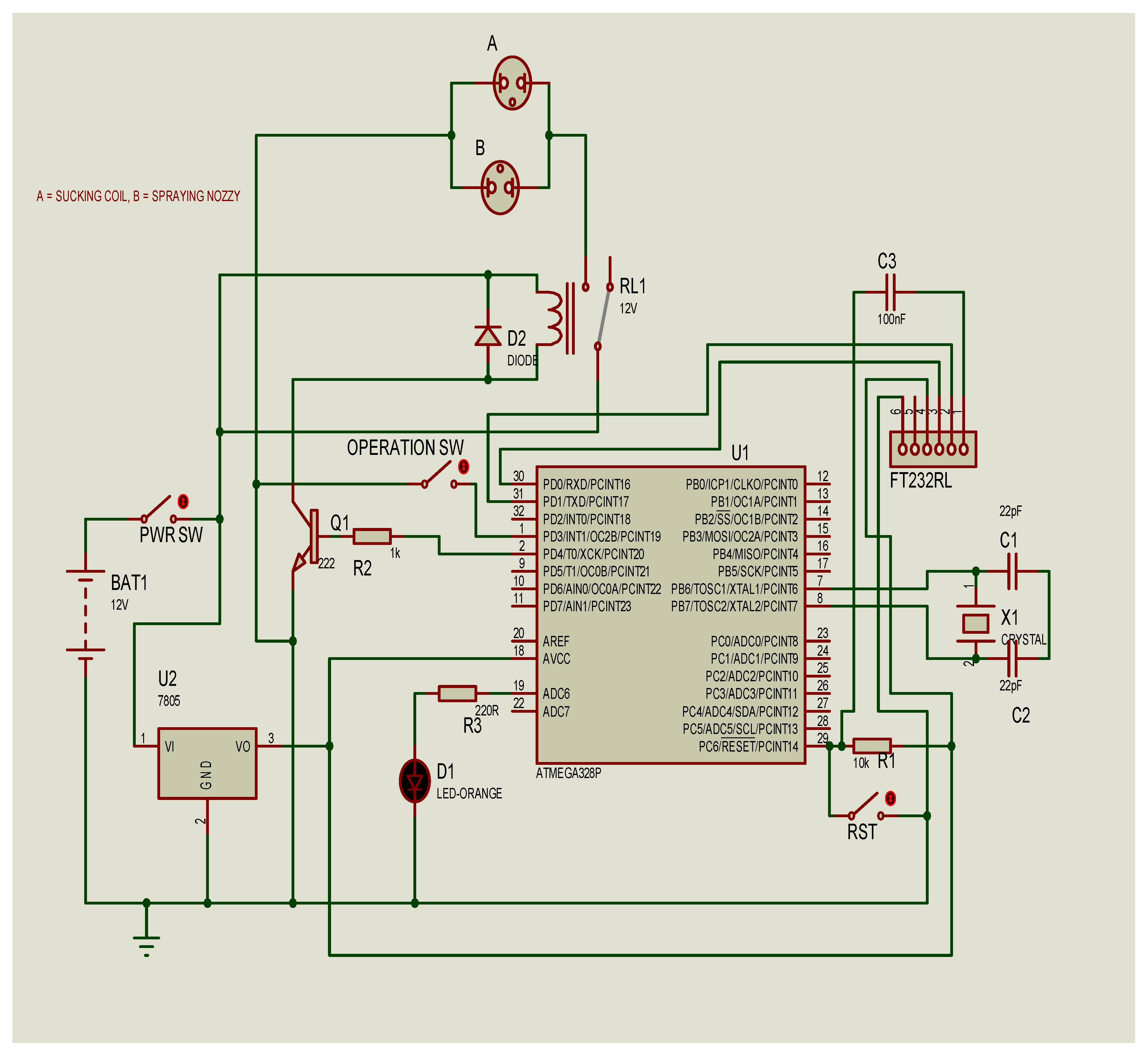
Figure 2.
(a) Flow rate of the precursors (b) Flow rate against current.
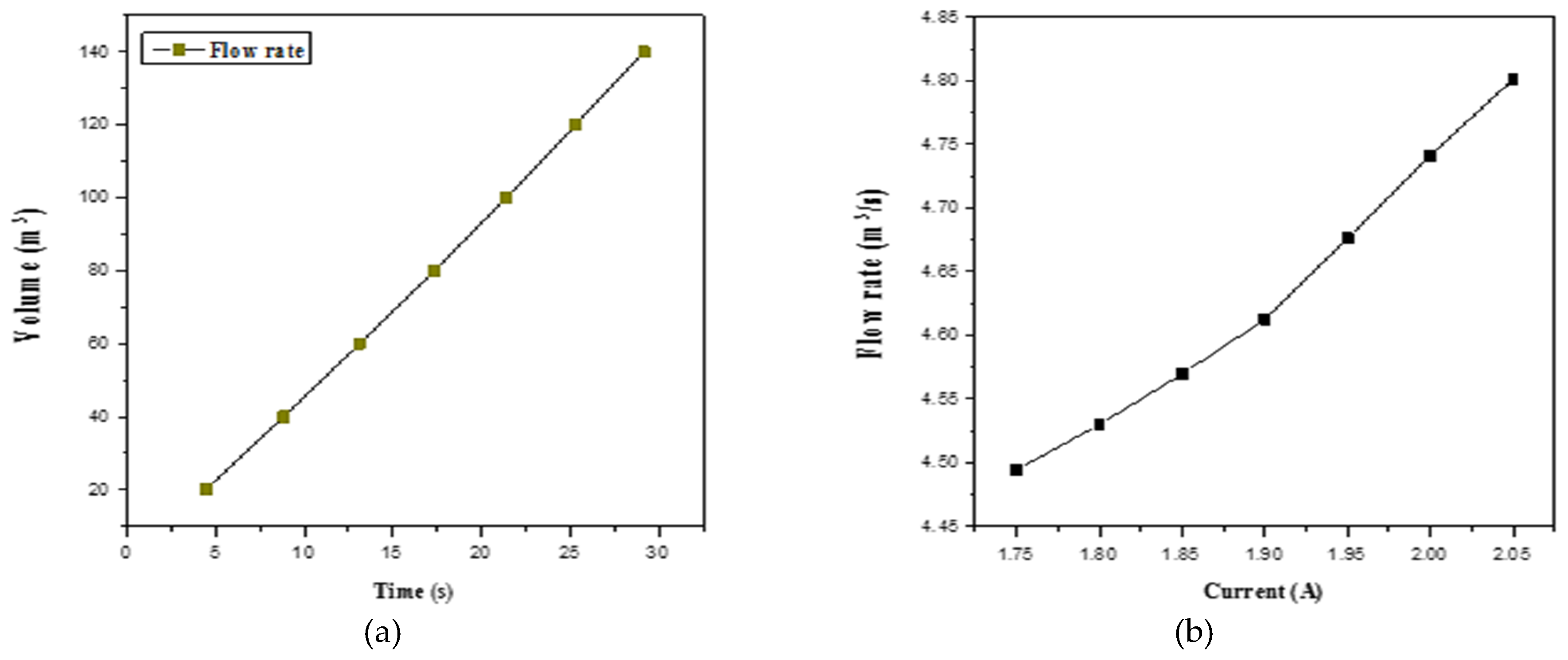
Figure 3.
SEM micrograph of Sample: (1) T0 (2) T1 (3) T2 and (4) T3.
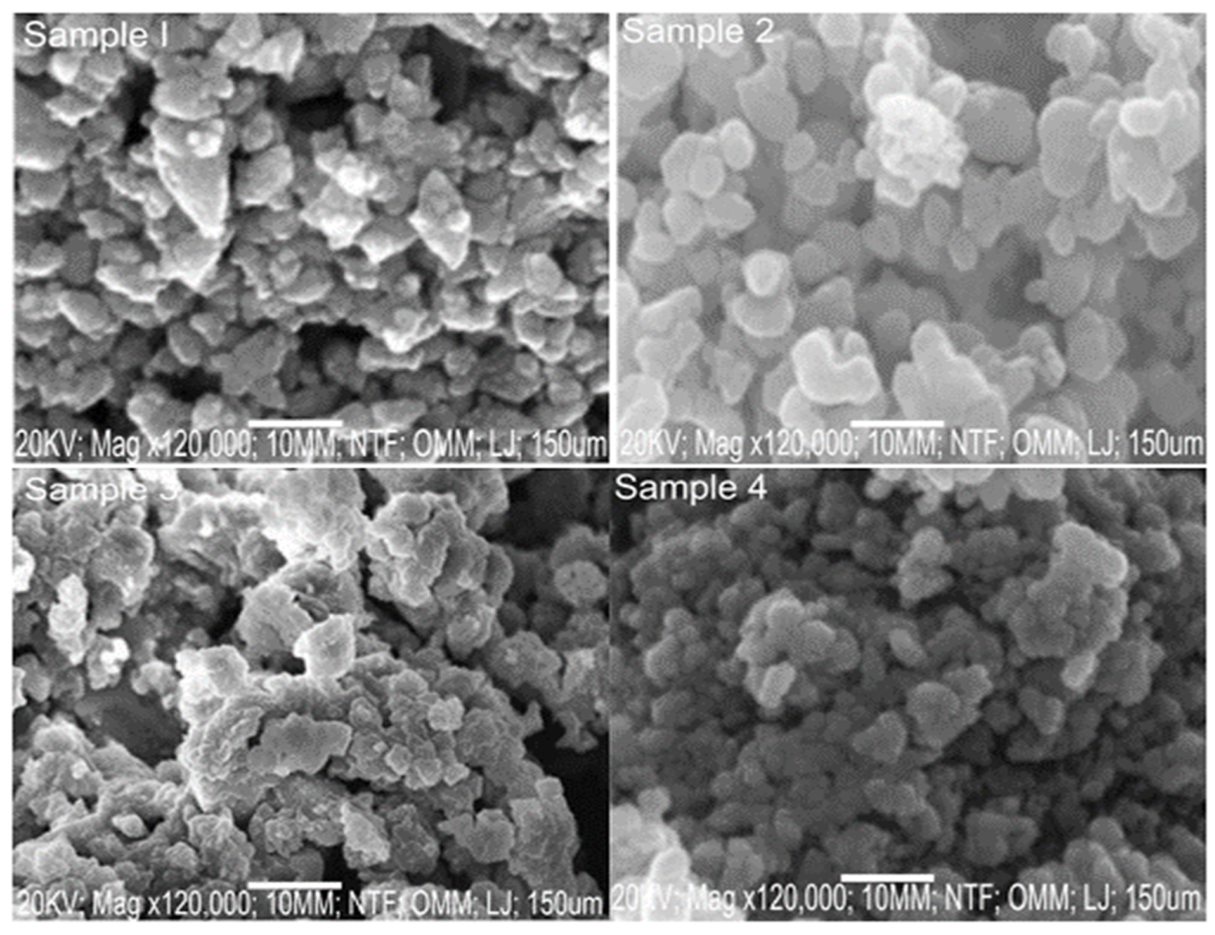
Figure 4.
EDX of samples: (a) T0 (b) T1 (c) T2 (d) T3.
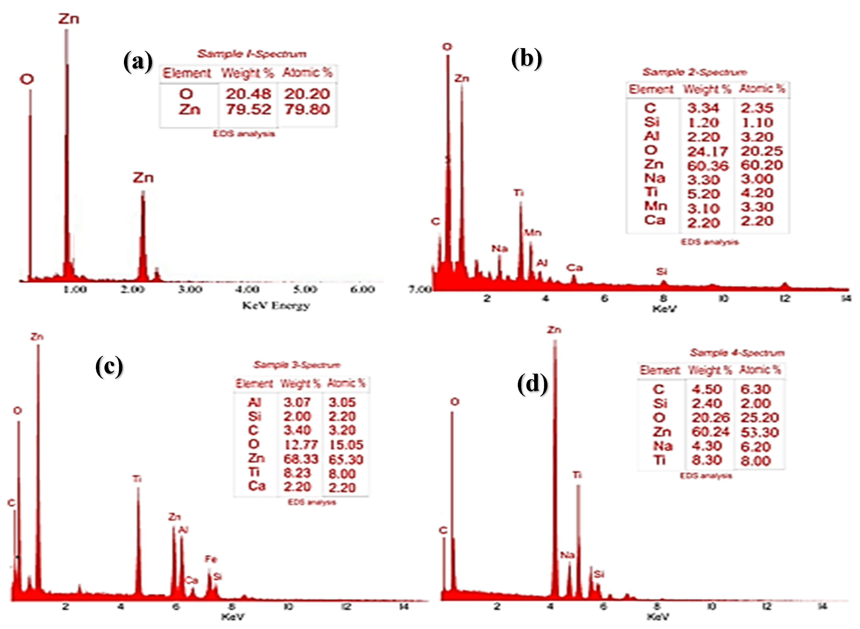
Figure 5.
I – V characteristics for T0 (a) and T1 –T3 (b).
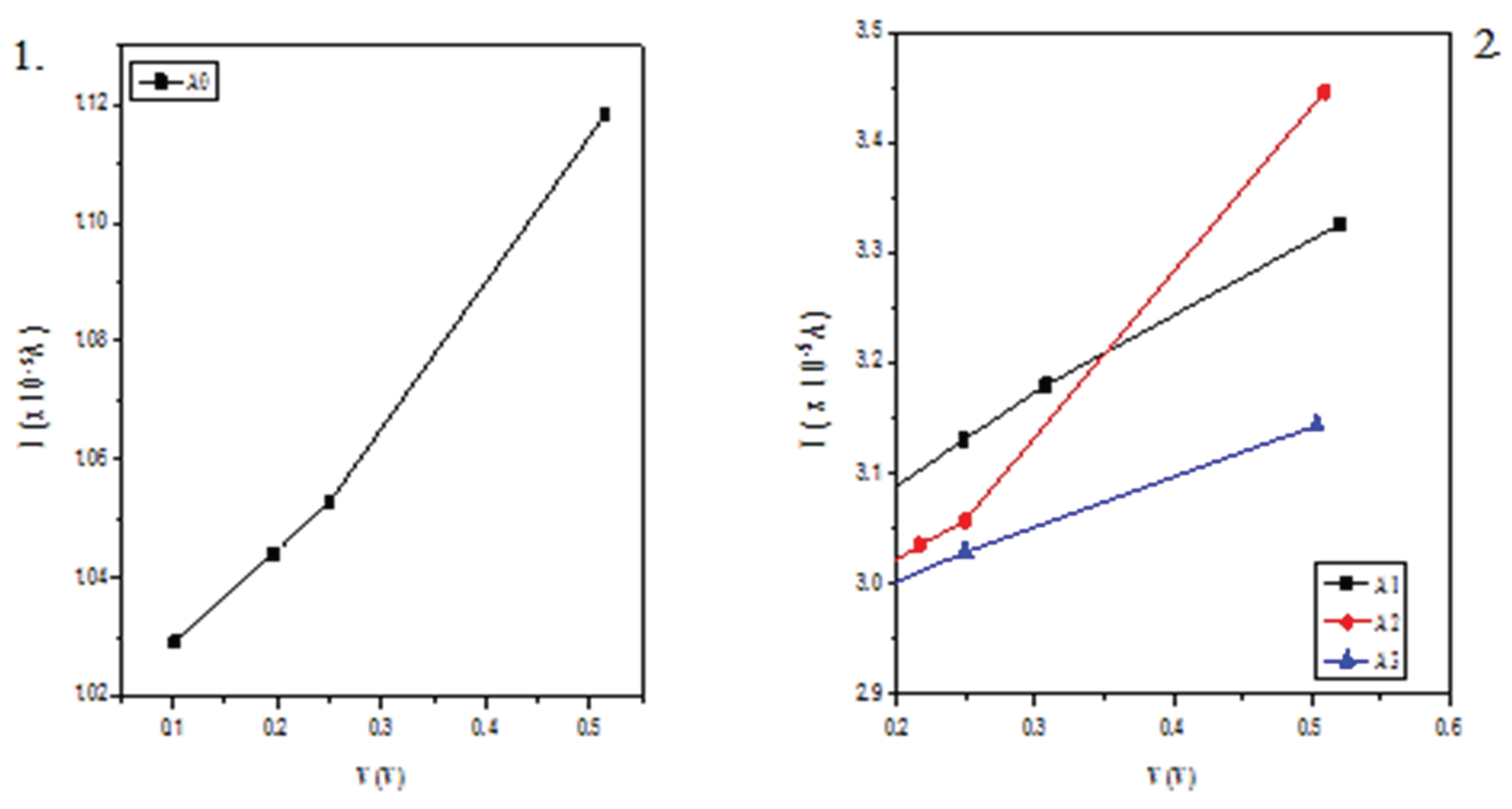

Table 1.
Samples, and its corresponding precursor amount.
| Sample Name | Precursor solutions |
|---|---|
| T0 | 100% ZnO (Control) |
| T1 | 97% ZnO with 3% Ti |
| T2 | 94% ZnO with 6% Ti |
| T3 | 91% ZnO with 9% Ti |
Table 2.
Effect of Ti Doping on the Elements present in ZnO Thin Films.
| Samples | Ti (%) | Zn (%) | O (%) | Si (%) | C (%) | Others (%) |
|---|---|---|---|---|---|---|
| T0 | - | 79.52 | 20.48 | - | - | - |
| T1 | 5.20 | 60.36 | 24.17 | 1.20 | 3.34 | 5.73 |
| T2 | 8.23 | 68.33 | 12.77 | 2.00 | 3.40 | 5.27 |
| T3 | 8.30 | 60.24 | 20.26 | 2.40 | 4.50 | 4.30 |
Disclaimer/Publisher’s Note: The statements, opinions and data contained in all publications are solely those of the individual author(s) and contributor(s) and not of MDPI and/or the editor(s). MDPI and/or the editor(s) disclaim responsibility for any injury to people or property resulting from any ideas, methods, instructions or products referred to in the content. |
© 2026 by the authors. Licensee MDPI, Basel, Switzerland. This article is an open access article distributed under the terms and conditions of the Creative Commons Attribution (CC BY) license (http://creativecommons.org/licenses/by/4.0/).
Copyright: This open access article is published under a Creative Commons CC BY 4.0 license, which permit the free download, distribution, and reuse, provided that the author and preprint are cited in any reuse.