Submitted:
17 February 2026
Posted:
19 February 2026
You are already at the latest version
Abstract
Flexible transparent conductive electrodes (TCEs) based on copper (Cu) meshes on polyethylene terephthalate (PET) substrates are constrained by critical interfacial weakness and inadequate mechanical durability, which hinder their widespread practical application. This study proposes a robust alloyed interface engineering strategy to address this fundamental challenge. Magnetron sputtering is employed to deposit Cu thin films on PET substrates with intermediate aluminum oxide (Al₂O₃) and nickel-chromium (NiCr) interfacial layers. Systematic comparative analyses reveal that the direct Cu/PET interface exhibits poor adhesion and mechanical fragility, while the incorporation of NiCr interlayers significantly enhances interfacial toughness. Through optimization, the NiCr layer forms a distinct alloyed interface with Cu via interdiffusion, fundamentally reinforcing the Cu/PET interface. Maskless photolithography enables precise patterning of Cu into micrometer-scale meshes, resulting in Cu Mesh/PET electrodes with excellent optoelectronic performance. The optimized electrodes achieve a sheet resistance of ~10.8 Ω/sq with an optical transmittance exceeding 87%, alongside remarkable mechanical robustness under repeated bending cycles. The synergistic toughening mechanism is clarified through interfacial microstructure analysis, which shows that the formation of a gradient alloyed zone effectively mitigates interfacial stress concentrations and suppresses crack propagation. This work provides a viable pathway for the development of next-generation durable flexible electronics.
Keywords:
flexible transparent conductive meshes
; Cu-based mesh electrodes
; interface stability
; flexible optoelectronics
1. Introduction
Flexible transparent conductive electrodes (TCEs) are indispensable components for advancing next-generation optoelectronic devices, including flexible displays, wearable sensors, and transparent heaters [1,2,3]. Indium tin oxide (ITO) currently dominates the market due to its exceptional optoelectronic performance, but its inherent brittleness and resource scarcity severely limit its application in flexible electronics [1]. As a result, alternative materials such as silver nanowires (AgNWs), carbon nanotubes (CNTs), and conductive polymers have been extensively explored [2]. Among these alternatives, copper (Cu) stands out as a particularly promising candidate due to its high intrinsic electrical conductivity (≈5.8 × 10⁷ S/m) and abundant availability in the Earth’s crust [4]. However, the practical implementation of Cu flexible electrodes on chemically inert polymer substrates is often hindered by weak interfacial adhesion and susceptibility to oxidation, highlighting the need for robust interface engineering strategies [4,5].
To address these interfacial challenges, various modification strategies have been proposed, yet each faces distinct limitations related to process compatibility or mechanical reliability. Some approaches utilize atomic layer deposition (ALD) to fabricate in-situ oxide interlayers, which can reduce electrical resistivity and enhance peel strength through oxide-metal bridging [6], but the low deposition rate of ALD and the complexity of vacuum processing impede high-throughput roll-to-roll manufacturing. Other strategies introduce refractory metal seed layers to promote adhesion via chemical bond formation at the interface [7], but the inherent stiffness of these metals often induces interfacial stress concentrations during small-radius bending, leading to premature crack initiation [8]. In terms of environmental stability, some methods develop oxidation-resistant Cu nanowires through specific chemical reactions, maintaining stable resistance in ambient air for extended periods [9], yet the synthesis complexity and potential haze introduced by the shell layer remain challenges for high-clarity optical integration.
To further overcome the optoelectronic limitations of continuous films, patterning Cu into micrometer-scale meshes has become a mainstream strategy to decouple optical transparency from electrical conductivity. Certain techniques employ self-cracking templates assisted by electrodeposition to fabricate semi-embedded Cu meshes, achieving ultra-low sheet resistance at high transmittance with a high Figure of Merit (FoM) [10], but the stochastic nature of crack propagation results in uncontrollable geometric uniformity and moiré patterns. Conventional photolithography, on the other hand, enables the fabrication of metal meshes with deterministic geometries and excellent uniformity [11], yet it relies heavily on expensive, pre-fabricated physical masks with fixed patterns, increasing fabrication costs and restricting flexibility for rapid prototyping or customized geometric designs. Maskless laser lithography has been utilized to construct fractal Cu meshes with excellent performance [12], but such approaches often focus heavily on geometric design while overlooking the critical role of the underlying seed layer in determining electromechanical durability. Therefore, developing a scalable electrode that simultaneously optimizes macroscopic geometry via precise patterning and microscopic interface via alloy engineering remains an urgent imperative.
This study reports high-performance Cu mesh electrodes developed through a systematic interface engineering strategy, rigorously comparing the efficacy of ceramic (Al2O3) and metallic (NiCr) seed layers. The ductile NiCr layer, activated by in-situ Ar plasma, significantly outperforms its brittle oxide counterpart as an interfacial bridge, as shown in Figure 1. It facilitates 5B-level adhesion via strong chemical anchoring and induces dense (111)-textured Cu growth. Consequently, the optimized Cu/NiCr thin films exhibit exceptional electromechanical durability (R/R0 < 5% after 1,000 cycles) and remarkable oxidation resistance under damp-heat conditions (85 °C/85% RH). Furthermore, leveraging maskless laser lithography, Cu meshes with high transmittance (87%) and low sheet resistance (10.8 Ω/sq) are fabricated, with practical viability validated in stable, rapid-response flexible heaters (>20 h of continuous operation).
2. Experimental Details
2.1. Fabrication of Cu Thin Films and Mesh Electrodes
Commercial polyethylene terephthalate (PET) films (~50 µm thick) are used as flexible substrates. Three distinct types of Cu thin films are prepared to systematically investigate the effect of interfacial layers on film performance: (1) Cu thin films without a seed layer, (2) Cu thin films with a NiCr seed layer, and (3) Cu thin films with an Al2O3 seed layer. Prior to deposition, the samples are loaded into a magnetron sputtering chamber (base pressure ≈ 8 × 10⁻⁴ Pa) and pretreated with in-situ argon (Ar) plasma (1 Pa, 2 min) to enhance surface energy. For seed layer deposition, the NiCr layer (~6 nm) is deposited via pulsed-DC sputtering (50 W, 0.33 Pa Ar), while the Al2O3 seed layer (~6 nm) is prepared via reactive sputtering at 70 W under a working pressure of 1 Pa, with an Ar:O2 gas flow ratio of 45:6 and a deposition time of 72 s. A Cu functional layer with a thickness of approximately 210 nm is then deposited on all samples using a polycrystalline Cu target via DC sputtering (200 W, 0.46 Pa Ar).
Following the optimization of the thin films, high-precision Cu mesh electrodes are fabricated using the NiCr seed layer via a photolithography-assisted lift-off process. A positive photoresist (AZ-5214) is spin-coated onto the cleaned PET substrates (300 rpm for 10 s, followed by 3000 rpm for 30 s) and soft-baked at 95 °C for 2 min. Unlike traditional mask alignment, the mesh patterns are defined using a maskless laser lithography system, controlled by a specific electronic mask program generated via MATLAB. After exposure and development (45 s), the optimal film stack (Ar plasma activation, NiCr seed layer, and Cu layer) is sequentially deposited under the aforementioned conditions. Finally, the lift-off process is performed by immersing the samples in acetone for 2 h followed by ultrasonication for 10 min to remove the photoresist and excess metal. The samples are stored at room temperature prior to optoelectronic and mechanical testing.
Two distinct aperiodic mesh geometries are designed and fabricated to optimize the trade-off between optoelectronic efficiency and mechanical flexibility: an aperiodic Linear mesh (Linear) composed of straight ligaments, and a stress-relieving aperiodic Sinusoidal mesh (Sinusoidal) featuring curved interconnected pathways. Both geometries are fabricated using the optimized NiCr layer process.
2.2. Characterization
The film thickness is determined via spectroscopic ellipsometry (J.A. Woollam, M2000DI). For structural and morphological characterization, the crystal structure is analyzed using X-ray diffraction (XRD, Bruker AXS D8 Advance) with Cu Kα radiation, while the surface morphologies and the quality of the mesh patterns are examined using a cold field-emission scanning electron microscopy (FE-SEM, Hitachi S-4800). Detailed interfacial microstructure and elemental distribution analyses are performed using a transmission electron microscope (TEM, FEI Tecnai F20) equipped with an energy-dispersive X-ray spectroscopy (EDS) system at an accelerating voltage of 200 kV. The surface roughness of the different seed layers is quantified by atomic force microscopy (AFM, Veeco Dimension 3100 V).
Regarding optoelectronic properties, the sheet resistance is measured using a four-point probe system (NAPSON, Cresbox), and transmittance spectra are acquired using a UV-vis-NIR spectrophotometer (Lambda950) equipped with an integrating sphere. Hall effect measurements are conducted to analyze carrier transport properties (mobility and concentration). The mechanical durability under repeated bending is evaluated using a flexible testing system (NAPSON, FlexTest mini-F-C) with a bending radius of 2 mm and a bending angle of 60°. Damp-heat aging tests are performed at 85 °C and 85% relative humidity (RH) to evaluate oxidation resistance and environmental tolerance, with electrical performance and surface morphology monitored every 20 min over a duration of 100 min.
For the practical application evaluation in flexible transparent heaters (FTHs), copper foil electrodes are attached to opposite edges of the Linear and Sinusoidal mesh films to ensure uniform current distribution. The time-dependent temperature profiles under a 5 V step voltage are recorded, and multi-voltage step heating experiments (3 V to 7 V) are conducted to assess thermal output controllability. Long-term operational reliability is evaluated under a constant bias of 5 V for over 20 h.
3. Results and Discussion
3.1. Influence of Seed Layers on Interfacial Stability and Microstructural Evolution
The robust integration of metallic thin films onto flexible polymer substrates is a prerequisite for reliable flexible optoelectronics, yet the chemical inertness of PET often leads to weak interfacial adhesion [3,13]. Standard cross-cut tape tests are conducted to quantitatively evaluate the efficacy of different interfacial layers, as shown in Figure 2a–c. The Cu without layer deposited directly on the PET substrate suffers from severe delamination, with the majority of the grid area peeling off. This failure is primarily attributed to the low surface energy of the polymer and the lack of reactive sites, resulting in weak physical adsorption. The introduction of an Al2O3 layer offers a marginal improvement, but extensive detachment persists along the cutting edges, indicating that the oxide-polymer interaction remains insufficient to withstand mechanical stress [14,15]. In contrast, the Cu/NiCr thin film maintains a pristine grid structure with sharp, intact edges, successfully achieving a 5B classification. This superior bonding is ascribed to the synergistic effect of Ar plasma activation and the metallic NiCr layer, which facilitates the formation of strong interfacial chemical bonds (e.g., Ni-O/Cr-O), thereby effectively anchoring the Cu layer to the substrate [16]. Atomic force microscopy (AFM) analysis further reveals that the interfacial layers significantly suppress surface roughness, as shown in Figure 2d–f. The Cu without layer (Figure 2d) exhibits a coarse morphology with a relatively high arithmetic average roughness (Rₐ) of 1.45 nm, indicative of a Volmer-Weber island growth mode [17,18]. The Cu/Al2O3 sample (Figure 2e) shows a reduced roughness of 0.64 nm, while the Cu/NiCr sample (Figure 2f) displays the densest and smoothest surface architecture, with the Rₐ value decreasing to a minimum of 0.43 nm. This ultra-smooth surface suggests that the NiCr layer promotes uniform nucleation and planar growth [19,20]. Correspondingly, X-ray diffraction (XRD) patterns demonstrate that all thin films exhibit characteristic face-centered cubic (fcc) Cu (111) and (200) peaks, as shown in Figure 2g. However, the Cu/NiCr thin film exhibits the sharpest and most intense (111) diffraction peak [11,21]. Calculations based on the Scherrer equation indicate that the average crystallite size increases from approximately 16.6 nm for the Cu without layer to 20.8 nm for the Cu/Al2O3 thin film and 21.1 nm for the Cu/NiCr thin film. This coarsening of grains confirms that the NiCr layer not only enhances adhesion but also promotes the texturing of Cu grains along the (111) orientation, resulting in a highly crystalline microstructure. The electrical properties of the Cu thin films are intrinsically governed by these microstructural characteristics [17,21]. The Cu/NiCr thin film exhibits superior electrical performance (Figure 2h), achieving the lowest sheet resistance of 0.218 Ω/sq and a resistivity of 4.40 µΩ·cm. In comparison, the Cu/Al2O3 and Cu without layer display higher resistivity values of 5.03 µΩ·cm and 5.38 µΩ·cm, respectively. Hall effect measurements reveal distinct differences in mobility and carrier concentration (Figure 2i). The Cu without layer displays a carrier mobility of 11.1 cm2/V·s and a carrier concentration of 1.05 × 1023 cm−3. Upon introducing the Al2O3 layer, the mobility increases to 12.8 cm2/V·s, attributed to the suppression of surface roughness scattering [22]. Conversely, the Cu/NiCr thin film exhibits a slightly reduced mobility of 10.2 cm2/V·s, despite possessing the smoothest surface. This reduction implies that while surface scattering is minimized, the diffusion of Ni and Cr atoms into the Cu lattice likely introduces point defects, acting as impurity scattering centers that impede electron transport [23,24]. Nevertheless, the Cu/NiCr thin film demonstrates a substantial increment in carrier concentration, reaching a maximum of 1.42 × 1023 cm−3. This high carrier density effectively offsets the mobility loss, thereby serving as the dominant factor responsible for the minimized resistivity.
Energy-dispersive X-ray spectroscopy (EDS) elemental mapping and quantitative analysis were performed to verify the elemental composition and confirm the incorporation of the interfacial layers (Figure 3). For the Cu/Al2O3 thin film, the EDS maps (Figure 3a–d) show a uniform distribution of Al and O species coexisting with the Cu matrix, indicating successful formation of the oxide interlayer. Quantitatively, Al is detected at 2.21 wt% (1.36 at%), with the detailed EDS spectral results summarized in the Supporting Information (Table S1). For the Cu/NiCr sample, Ni and Cr signals are clearly resolved in the corresponding EDS maps (Figure 3e–h) and spectra (Figure 3j), with concentrations of 1.42 wt% (1.53 at%) for Ni and 1.01 wt% (1.23 at%) for Cr (Table S1). Notably, the detection of these elements despite the ultrathin interfacial layer thickness (∼6 nm) confirms the successful construction of the targeted Cu/NiCr architecture. Moreover, the presence of Ni and Cr supports the proposed mechanism (Figure 1), wherein solute atoms reinforce the interface and modulate the nucleation kinetics of the overlying Cu film [25].
The superior adhesion of the Cu/NiCr interface is attributed to the synergistic interaction of both nickel (Ni) and chromium (Cr) elements with the substrate. Upon deposition on the plasma-activated PET surface, the high-energy metallic atoms (Ni and Cr) collectively react with the abundant oxygen-containing functional groups (e.g., C=O, –OH), establishing a robust chemical bonding network (metal–O–C). Specifically, Cr serves as a reactive anchor by forming strong covalent bonds due to its high oxygen affinity, while Ni, as the chemically stable matrix, promotes the formation of a dense, continuous interfacial layer that physically interlocks with the polymer surface [26]. This cooperative mechanism effectively prevents the localized delamination often observed in single-component interfaces, ensuring 5B-level adhesion strength. Furthermore, unlike the abrupt boundary formed with ceramic seed layers (e.g., Al2O3), the Cu/NiCr interface facilitates the formation of a metallic solid solution. Since Copper (Cu) and Nickel (Ni) share the same face-centered cubic (FCC) crystal structure and similar atomic radii, they exhibit complete solid solubility. This allows for the interdiffusion of Ni and Cu atoms, creating a graded transition zone rather than a sharp interface [27]. As evidenced by the EDS mapping (Figure 3h), this interdiffusion layer effectively bridges the lattice mismatch and enhances interfacial toughness, thereby suppressing void formation and crack initiation under mechanical stress.
3.2. Electromechanical Reliability and Environmental Stability
The surface morphology and electromechanical stability of the films under dynamic deformation are systematically investigated. Scanning electron microscopy (SEM) images of the as-deposited thin films show that both the Cu thin film without a seed layer and the Cu/Al2O3 thin film exhibit a granular morphology characterized by discernible voids and loose grain boundaries (Figure 4a–c). In contrast, the Cu/NiCr thin film displays a highly compact, pinhole-free, and continuous surface architecture, confirming that the metallic NiCr layer promotes high-quality, dense thin film growth [5,19]. Dynamic bending tests with a bending radius (R) of 2 mm and a bending angle of 60° reveal distinct degradation behaviors among the three samples, as shown in Figure 4d-f. The Cu/Al2O3 thin film undergoes rapid electromechanical degradation, with the normalized resistance (R/R0) surging to ≈ 2.7 after only 400 cycles. This abrupt failure is attributed to the inherent brittleness of the ceramic oxide layer, which is prone to fracture under tensile stress, subsequently severing the conductive Cu network [28]. The Cu thin film without a seed layer shows a gradual increase in resistance, reaching R/R0 ≈ 1.8 after 1000 cycles, primarily due to the accumulation of fatigue cracks and localized delamination caused by weak interfacial adhesion. Remarkably, the Cu/NiCr thin film demonstrates exceptional durability, with the resistance remaining negligible (R/R0 ≈ 1.0) throughout the 1,000 bending cycles. The evolution of Hall mobility during bending further elucidates the microscopic degradation mechanism. For the Cu/NiCr thin film, the mobility is maintained at a stable level, indicating that the electron transport channels remain intact without significant scattering induced by structural defects. Conversely, the mobility of the Cu/Al2O3 thin film exhibits a precipitous decay, confirming that the generation of high-density cracks acts as a severe scattering source for charge carriers. Post-bending SEM characterization corroborates these findings (Figure 4g–i): the bent Cu/Al2O3 surface is characterized by dense, transverse microcracks, the Cu thin film without a seed layer exhibits visible crack propagation and signs of localized detachment, while the Cu/NiCr thin film retains a smooth, continuous, and crack-free morphology even after 1,000 cycles. This superior bending fatigue resistance confirms that the ductile NiCr alloy layer not only strengthens interfacial adhesion but also effectively dissipates mechanical stress, thereby suppressing crack initiation and propagation [23].
Damp-heat aging tests at 85 °C and 85% relative humidity (RH) are conducted to evaluate the long-term operational reliability of the films under harsh environmental conditions, as shown in Figure 5. The Cu thin film without a seed layer and the Cu/Al2O3 thin film exhibit pronounced oxidative degradation, with visible oxidation spots and localized corrosion pits emerging rapidly within the first 40 min and expanding significantly as the aging time extends. This severe surface discoloration suggests that moisture and oxygen molecules easily penetrate the loosely packed grain boundaries, facilitating oxidative corrosion [11,29,30]. In contrast, the Cu/NiCr thin film demonstrates significantly enhanced resistance to environmental corrosion, with only minor, localized oxidation spots observed after prolonged exposure. The quantitative evolution of electrical properties during aging shows that all samples exhibit a decreasing trend in sheet resistance (Rs) and normalized resistance (R/R0) during the initial stage, primarily attributed to the thermal annealing effect at 85 °C, which promotes grain growth and defect annihilation [31]. However, the magnitude of this change varies significantly: the Cu thin film without a seed layer and Cu/Al2O3 thin film show a sharp resistance drop (R/R0 decreases to ≈0.8), indicative of the annealing of a high density of pre-existing defects and structural instability under thermal stress. Conversely, the Cu/NiCr thin film exhibits the highest stability, with the resistance showing only a marginal fluctuation (R/R0 stabilizes around 0.9). Post-aging AFM characterization further corroborates the protective mechanism of the NiCr layer: the surfaces of the aged Cu thin film without a seed layer and Cu/Al2O3 thin film appear rough and uneven, with Rₐ values increasing to 3.94 nm and 4.45 nm, respectively, while the Cu/NiCr thin film retains a remarkably smooth and dense surface topology with the lowest Rₐ of 1.55 nm. This result confirms that the dense packing of Cu (111) grains induced by the NiCr layer acts as an effective diffusion barrier against water vapor and oxygen, thereby significantly enhancing the environmental lifespan of the electrode [30].
3.3. Geometric Engineering for Electromechanical Optimization
Conventional periodic metal meshes often suffer from coherent optical interference, leading to distinct diffraction artifacts and Moiré patterns when overlaid on pixel arrays [32]. Aperiodic or random mesh designs can effectively suppress these coherent diffraction effects, minimizing Moiré patterns to achieve superior optical homogeneity and visual invisibility [33,34]. Quantitative comparisons from the literature are compiled in the Supporting Information (Table S2). These reports indicate that introducing aperiodicity reduces the non-uniformity of high-order diffraction (Cv) and weakens concentrated high-order stray-light components, which in turn alleviates diffraction-related artifacts and Moiré visibility. The reported sheet resistance remains comparable to, or better than, that of periodic meshes. Further numerical details and references are provided in Table S2.
Motivated by this optical advantage, an aperiodic tessellation strategy is adopted for the electrode design, with two distinct aperiodic mesh geometries fabricated: an aperiodic Linear mesh (Linear) and a stress-relieving aperiodic Sinusoidal mesh (Sinusoidal) [35]. Metallographic micrographs (Figure 6a,b) show that both the Linear and Sinusoidal samples exhibit highly uniform network structures with well-defined edges, comparable to commercial metal mesh films. A macroscopic photograph (Figure 6c) visually demonstrates the excellent optical clarity of the mesh electrodes, allowing for distinct visibility of the background features. The theoretical optical aperture ratio (AR) is calculated based on the geometric lattice definition, and the Figure of Merit (FoM) is calculated using the ratio of DC conductivity to optical conductivity [36]. In terms of static optoelectronic properties, the Linear mesh exhibits a sheet resistance (Rs) of 10.8 Ω/sq, an aperture ratio of 96%, and a high transmittance of 87.0% at 550 nm, as shown in Figure 6d–f. In comparison, as summarized in Table 1, the Sinusoidal mesh demonstrates a marginally lower sheet resistance of 10.4 Ω/sq and an aperture ratio of 95.9%, but its transmittance is lower at 85.7%. Consequently, despite the slightly higher resistance, the Linear mesh yields a superior FoM of 121.3, compared to 102.1 for the Sinusoidal mesh. This quantitative analysis indicates that the Linear design, with its higher aperture ratio and transmittance, offers a higher static optoelectronic performance. This quantitative analysis indicates that the Sinusoidal design, with its higher aperture ratio and transmittance, offers a more favorable balance between transparency and conductivity. Bending fatigue tests reveal a stark contrast in stability between the two geometries, as shown in Figure 6g–i. The Linear mesh undergoes rapid electromechanical degradation, with the normalized resistance (R/R0) surging to ≈ 4.7 after 2,500 bending cycles. Post-bending microscopic analysis shows severe transverse fractures concentrated at the sharp hexagonal vertices, severing the electrical network. In contrast, the Sinusoidal mesh demonstrates superior durability, with the resistance increase significantly suppressed (R/R0 ≈ 2.8) under identical conditions. The Sinusoidal structure remains continuous without observable cracking, as the Sinusoidal curvature effectively acts as a mechanical spring, delocalizing tensile stress along the arcs rather than concentrating it at the junctions [37,38]. Consequently, although the Linear mesh possesses a higher static FoM, the Sinusoidal geometry provides a critical enhancement in electromechanical reliability via geometric compliance, rendering it the preferred candidate for highly flexible electronic applications.
3.4. Practical Application in Flexible Transparent Heaters
To validate the practical viability of the fabricated electrodes, flexible transparent heaters (FTHs) are assembled using Linear and Sinusoidal thin films (Figure 7) [39]. The time-dependent temperature profiles under a 5 V step voltage reveal a rapid thermal response: the surface temperature rises from room temperature (∼20 °C) to thermal equilibrium within approximately 40 s and swiftly returns to the initial state upon power-off. The Linear heater achieves a higher saturation temperature of 49.8 °C, whereas the Sinusoidal heater stabilizes at 42.9 °C. This discrepancy is governed by the Joule heating mechanism (P = V2/R), where the lower sheet resistance of the Linear mesh generates a higher power density compared to the Sinusoidal counterpart. Multi-voltage step heating experiments demonstrate precise controllability of the thermal output. As the applied voltage is incrementally stepped from 3 V to 7 V, the saturation temperature of the Linear heater increases monotonically from 30.4 °C to a maximum of 73.6 °C. Similarly, the Sinusoidal heater exhibits stable temperature plateaus ranging from 27.7 °C to 62.1 °C. The observed quadratic dependence of temperature on input voltage enables accurate, wide-range thermal tuning suitable for applications such as defogging systems and wearable thermotherapy [35,40]. Long-term operational reliability evaluated under a constant bias of 5 V for over 20 h shows that both devices exhibit exceptional stability, characterized by negligible resistance drift and constant thermal output throughout the testing duration. The maintenance of stable heating profiles (Linear at ∼50 °C and Sinusoidal at ∼43 °C) confirms robust resistance against thermal degradation. This superior electro-thermal stability is attributed to the dense NiCr layer, which acts as a robust diffusion barrier, effectively mitigating oxidation kinetics and preventing the inter-diffusion of species at elevated temperatures [41]. These results confirm that both mesh designs offer viable technical solutions for high-performance heaters, with the Linear design maximizing thermal efficiency and the Sinusoidal design offering a superior balance of mechanical compliance and optoelectronic performance.
4. Conclusions
This work presents a robust alloyed interface engineering strategy to address the critical interfacial adhesion weakness and inadequate mechanical durability of Cu-based flexible transparent conductive electrodes (TCEs) on PET substrates. Systematic comparative studies of ceramic (Al2O3) and metallic (NiCr) seed layers reveal that the NiCr layer forms a distinct alloyed interface with Cu via interdiffusion, which fundamentally reinforces the Cu/PET interface. The optimized Cu/NiCr thin films achieve 5B-level adhesion, a low sheet resistance of 0.218 Ω/sq, exceptional electromechanical durability (R/R0 < 5% after 1,000 bending cycles), and remarkable environmental stability under damp-heat conditions. By leveraging maskless photolithography, Cu is precisely patterned into micrometer-scale aperiodic meshes. Among the designed geometries, the Linear mesh exhibits superior optoelectronic performance, achieving ~10.8 Ω/sq sheet resistance, >87% optical transmittance, and a high FoM of 121.3, while the Sinusoidal mesh offers a superior mechanical flexibility. Practical validation in flexible transparent heaters (FTHs) confirms rapid thermal response, precise temperature controllability, and long-term operational stability (>20 h), underscoring the electrodes’ potential for next-generation flexible optoelectronics. Microstructural analysis clarifies the synergistic toughening mechanism: the gradient alloyed zone formed at the Cu-NiCr interface effectively mitigates interfacial stress concentrations and suppresses crack propagation. This work provides a viable pathway for developing high-performance, durable flexible TCEs, offering valuable insights for the design and optimization of next-generation flexible electronic devices.
Supplementary Materials
The following supporting information can be downloaded at the website of this paper posted on Preprints.org.
Author Contributions
Hongliang Zhang, Weijie Song: Supervision, Project administration, Funding acquisition. Jia Li, Xianfa Rao: Writing–review & editing. Xueyu Li, Jingwu Wang, Bing chen: Validation, Data curation. Chengli Zhang, Qiang Wang: Supervision, Resources, Project administration. Guanglong Xu: Methodology, Data curation. Xiao Lu: Writing–original draft, Validation, Methodology, Investigation, Data curation.
Data Availability Statement
The data supporting this article have been included as part of the ESI.
Acknowledgments
This project is supported by the “Pioneer” and “Leading Goose” R&D Program of Zhejiang (2024C01252(SD2)).
Conflicts of Interest
The authors declare that they have no known competing financial interests or personal relationships that could have appeared to influence the work reported in this paper.
References
- Yang, Y.; Wang, Y.; Qiao, Y.; Song, Y. Flexible transparent electrodes based on metallic micro–nano architectures for perovskite solar cells. J. Mater. Chem. C 2022, 10, 2349–2363. [Google Scholar] [CrossRef]
- Ding, Y.; Xiong, S.; Sun, L.; Wang, Y.; Zhou, Y.; Li, Y.; Peng, J.; Fukuda, K.; Someya, T.; Liu, R.; et al. Metal nanowire-based transparent electrode for flexible and stretchable optoelectronic devices. Chem. Soc. Rev. 2024, 53, 7784–7827. [Google Scholar] [CrossRef]
- Zhang, Y.; Lu, Z.; Zhou, X.; Xiong, J. Metallic meshes for advanced flexible optoelectronic devices. Mater. Today 2024, 73, 179–207. [Google Scholar] [CrossRef]
- Kim, J.; Kim, M.; Jung, H.; Park, J.; Lee, Y. Ultrastable 2D material-wrapped copper nanowires for high-performance flexible and transparent energy devices. Nano Energy 2023, 106, 108067. [Google Scholar] [CrossRef]
- Lu, M.; You, J.; Gao, M.; Li, W.; Zhang, C.; Zhu, B.; Peng, C.; Wu, S.; Dazhenlamu; Ren, W.; et al. Interfacial adhesion in flexible electronics: Materials, structures and applications. Coord. Chem. Rev. 2025, 523, 216278. [Google Scholar] [CrossRef]
- Gao, Z.; Zhang, C.; Gao, J.; Wang, Q.; Xu, G.; Cao, H.; Zhang, H. Nucleation and growth of low resistivity copper thin films on polyimide substrates by low-temperature atomic layer deposition. Appl. Surf. Sci. 2023, 638, 158072. [Google Scholar] [CrossRef]
- Nimbalkar, P.; Blancher, C.; Kathaperumal, M.; Swaminathan, M.; Tummala, R. Effect of titanium-polymer interactions on adhesion of polymer-copper redistribution layers in advanced packaging. IEEE Trans. Device Mater. Reliab 2022, 22, 59–64. [Google Scholar] [CrossRef]
- Xia, Y.; Xie, Z.; Zuo, J.; Wu, K.; Yao, X.; Liu, G.; Sun, J. Fatigue tolerance of nanostructured Cu/interlayer bilayers: Tuned by heterogeneous interface. Scr. Mater. 2023, 234, 115563. [Google Scholar] [CrossRef]
- Križan, A.; Bardet, L.; Zimny, K.; Romanus, M.; Berthe, M.; Labrugère-Sarroste, C.; Bellet, D.; Tréguer-Delapierre, M. Oxidation-resistant Cu-based nanowire transparent electrodes activated by an exothermic reduction reaction. ACS Nano 2024, 18, 34902–34911. [Google Scholar] [CrossRef] [PubMed]
- Chen, Z.; Yang, S.; Huang, J.; Gu, Y.; Huang, W.; Liu, S.; Lin, Z.; Zeng, Z.; Hu, Y.; Chen, Z.; et al. Flexible, transparent and conductive metal mesh films with ultra-high FoM for stretchable heating and electromagnetic interference shielding. Nano-Micro Lett. 2024, 16, 92. [Google Scholar] [CrossRef]
- Kim, S.J.; Kim, Y.I.; Lamichhane, B.; Kim, Y.-H.; Lee, Y.; Cho, C.R.; Cheon, M.; Kim, J.C.; Jeong, H.Y.; Ha, T.; et al. Flat-surface-assisted and self-regulated oxidation resistance of Cu(111). Nature 2022, 603, 434–438. [Google Scholar] [CrossRef]
- Li, T.; Chen, X.; Xu, Z.; Nie, S.; Xu, W.; Yuan, W.; Xu, S.; Zhang, S.; Pei, F.; Su, W.; et al. High-performance visible-infrared broadband transparent copper mesh conductor and applications for electromagnetic shielding and heating. Sci. China Mater. 2025, 68, 421–431. [Google Scholar] [CrossRef]
- Prakash, A.; Manohara, K.; Kumar, S.; Katiyar, M. Effect of plasma processing on the morphological and electrical properties of polyethylene terephthalate (PET) substrate. Results Surf. Interfaces 2025, 20, 100559. [Google Scholar] [CrossRef]
- Putz, B.; Edwards, T.E.J.; Huszar, E.; Pethö, L.; Kreiml, P.; Cordill, M.J.; Thiaudiere, D.; Chiroli, S.; Zighem, F.; Faurie, D.; et al. In situ fragmentation of Al/Al2O3 multilayers on flexible substrates in biaxial tension. Mater. Des. 2023, 232, 112081. [Google Scholar] [CrossRef]
- Petit, R.R.; Li, J.; Van De Voorde, B.; Van Vlierberghe, S.; Smet, P.F.; Detavernier, C. Atomic layer deposition on polymer thin films: On the role of precursor infiltration and reactivity. ACS Appl. Mater. Interfaces 2021, 13, 46151–46163. [Google Scholar] [CrossRef]
- Wei, F.; Wei, Y.; Yao, X.; Li, X.; Wei, Z.; Zhang, S.; Luo, X.; Guo, Z.; Liu, Q.; Zhu, Q. Review: Enhancing bond strength of heterogeneous metal-polymer components the perspective of surface micro-nano morphology construction. J. Mater. Sci. 2025, 60, 6023–6058. [Google Scholar] [CrossRef]
- Dulmaa, A.; Cougnon, F.G.; Dedoncker, R.; Depla, D. On the grain size-thickness correlation for thin films. Acta Mater. 2021, 212, 116896. [Google Scholar] [CrossRef]
- Wang, X.; Jin, P.; Xiao, D.; Lu, Y.; Tian, X. Interlayer design for strong adhesion in the double-layer flexible copper clad laminate via HiPIMS deposition. Appl. Surf. Sci. 2024, 670, 160697. [Google Scholar] [CrossRef]
- Tsai, Y.-N.; Chen, H.-Y.; Tseng, I.-H.; Lee, J.-W.; Tsai, M.-H.; Li, M.-S.; Wang, C.-H.; Gee, C.-M.; Chen, T.-L.; Tsai, P.-C. Adhesive properties of deposited Cu films on colorless polyimide using high power impulse magnetron sputtering system. Surf. Coat. Technol. 2024, 484, 130710. [Google Scholar] [CrossRef]
- Lin, J.; Kilani, M.; Baharfar, M.; Wang, R.; Mao, G. Understanding the nanoscale phenomena of nucleation and crystal growth in electrodeposition. Nanoscale 2024, 16, 19564–19588. [Google Scholar] [CrossRef]
- Peng, W.; Gao, J.; Lu, T.; Sun, B.; Zhang, X.; Zhang, L.; Tu, S. Insights into abnormal grain growth in copper thin films for reduced electrical resistivity: A quantitative multi-order-parameter phase-field study under finite element framework. Acta Mater. 2023, 260, 119236. [Google Scholar] [CrossRef]
- Hu, C.; Zhang, Y.; Chen, Z.; Zhang, Q.; Zhu, J.; Hu, S.; Ke, Y. Size effect of resistivity due to surface roughness scattering in alternative interconnect metals: Cu, Co, Ru, and Mo. Phys. Rev. B 2023, 107, 195422. [Google Scholar] [CrossRef]
- Lee, K.-P.; Tran, D.-P.; Chen, B.-Y.; Lin, Y.-Q.; Huang, J.-Y.; Chen, P.-C.; Chen, C. Twin boundary and grain boundary engineering to enhance mechanical strength of nanotwinned Cu. Mater. Sci. Eng. A 2025, 923, 147719. [Google Scholar] [CrossRef]
- Bishara, H.; Langenohl, L.; Zhou, X.; Gault, B.; Best, J.P.; Dehm, G. Decoupling the electrical resistivity contribution of grain boundaries in dilute Fe-alloyed Cu thin films. Scr. Mater. 2023, 230, 115393. [Google Scholar] [CrossRef]
- Chang, L.; Yang, G.; Zhu, H.; Li, Y.; Li, L. Chloride–gelatin regulation of ion transport and 2D nucleation selects (110)/(111) textures in electrodeposited nanotwinned copper. J. Mater. Sci. 2026, 61, 671–685. [Google Scholar] [CrossRef]
- Selimov, A.; Chu, K.; McDowell, D.L. Effects of interdiffusion on shear response of semi-coherent {111} interfaces in Ni/Cu. Int. J. Plast. 2022, 157, 103393. [Google Scholar] [CrossRef]
- Wang, G.; Wang, Z.; Ren, J.; Wu, Z.; Duan, Y. Innovative stress-release method for low-stress flexible Al2O3 encapsulation films in OLED applications. npj Flex. Electron. 2025, 9, 94. [Google Scholar] [CrossRef]
- Jeong, E.; Lee, S.-G.; Yu, S.M.; Mun, C.; Han, S.Z.; Lee, G.-H.; Choi, E.-A.; Yun, J. Cu-substrate interfacial adhesion: A key factor in controlling the oxidation of Cu thin films on oxide substrates. Appl. Surf. Sci. 2023, 640, 158319. [Google Scholar] [CrossRef]
- Fang, Y.; Wang, Y.; Bian, Y.; Ngiam, Y.; Huang, M.X. Enhancing oxidation resistance of Cu thin film through grain size reduction. Acta Mater. 2026, 302, 121676. [Google Scholar] [CrossRef]
- Bishara, H.; Lee, S.; Brink, T.; Ghidelli, M.; Dehm, G. Understanding grain boundary electrical resistivity in Cu: The effect of boundary structure. ACS Nano 2021, 15, 16607–16615. [Google Scholar] [CrossRef]
- Zhou, H.; Song, Y. Fabrication of silver mesh/grid and its applications in electronics. ACS Appl. Mater. Interfaces 2021, 13, 3493–3511. [Google Scholar] [CrossRef] [PubMed]
- Wang, Z.; Wang, M.; Jiao, B.; Lu, W.; Xu, D.; Huang, L.; Hou, X.; Wu, Z. Smooth and mechanically robust random metallic mesh electrode modified by thermally transferred PEDOT: PSS for ITO-free flexible organic light-emitting diodes. Org. Electron. 2022, 106, 106498. [Google Scholar] [CrossRef]
- Zarei, M.; Li, M.; Medvedeva, E.E.; Sharma, S.; Kim, J.; Shao, Z.; Walker, S.B.; LeMieux, M.; Liu, Q.; Leu, P.W. Flexible embedded metal meshes by sputter-free crack lithography for transparent electrodes and electromagnetic interference shielding. ACS Appl. Mater. Interfaces 2024, 16, 6382–6393. [Google Scholar] [CrossRef]
- Kim, H.-J.; Kim, Y. Copper micromesh-based lightweight transparent conductor with short response time for wearable heaters. Micro Nano Syst. Lett. 2021, 9, 6. [Google Scholar] [CrossRef]
- Ellmer, K. Past achievements and future challenges in the development of optically transparent electrodes. Nat. Photonics 2012, 6, 809–817. [Google Scholar] [CrossRef]
- Yang, S.; Cao, Y.-J.; Han, K.; Guo, J.-T.; Zheng, P.-L.; Wang, L.-Y.; Cheng, T.; Zhang, Y.-Z.; Lai, W.-Y. Stretchable transparent electrodes based on metal grid hybrids for skin-like multimodal sensing and flexible touch panel. Nano Energy 2025, 139, 110942. [Google Scholar] [CrossRef]
- Jiao, R.; Wang, R.; Wang, Y.; Cheung, Y.K.; Chen, X.; Wang, X.; Deng, Y.; Yu, H. Vertical serpentine interconnect-enabled stretchable and curved electronics. Microsyst. Nanoeng. 2023, 9, 149. [Google Scholar] [CrossRef]
- Kim, H.-J.; Choi, D.-I.; Lee, S.; Sung, S.-K.; Kang, D.-H.; Kim, J.; Kim, Y. Quick thermal response-transparent-wearable heater based on copper mesh/poly(vinyl alcohol) film. Adv. Eng. Mater. 2021, 23, 2100395. [Google Scholar] [CrossRef]
- Liang, R.; Wang, H.; Zhan, S.; Ye, M.; Shu, L.; Fei, L.; Wang, D.; Zheng, R.; Ke, S. High-temperature flexible transparent heater for rapid thermal annealing of thin films. Phys. Rev. Appl. 2022, 17, 044049. [Google Scholar] [CrossRef]
- Liu, S.; Chen, Y.; An, Z.; Zhao, J.; Lu, H.; Jiao, Y.; Xie, L.; Li, A.; Han, X. Microstructure and oxidation of NiCr alloys studied by analytical in situ environmental TEM. Corros. Sci. 2023, 224, 111525. [Google Scholar] [CrossRef]
Figure 1.
Schematic illustration of the fabrication process and structural design for alloy-engineered Cu mesh electrodes.
Figure 1.
Schematic illustration of the fabrication process and structural design for alloy-engineered Cu mesh electrodes.
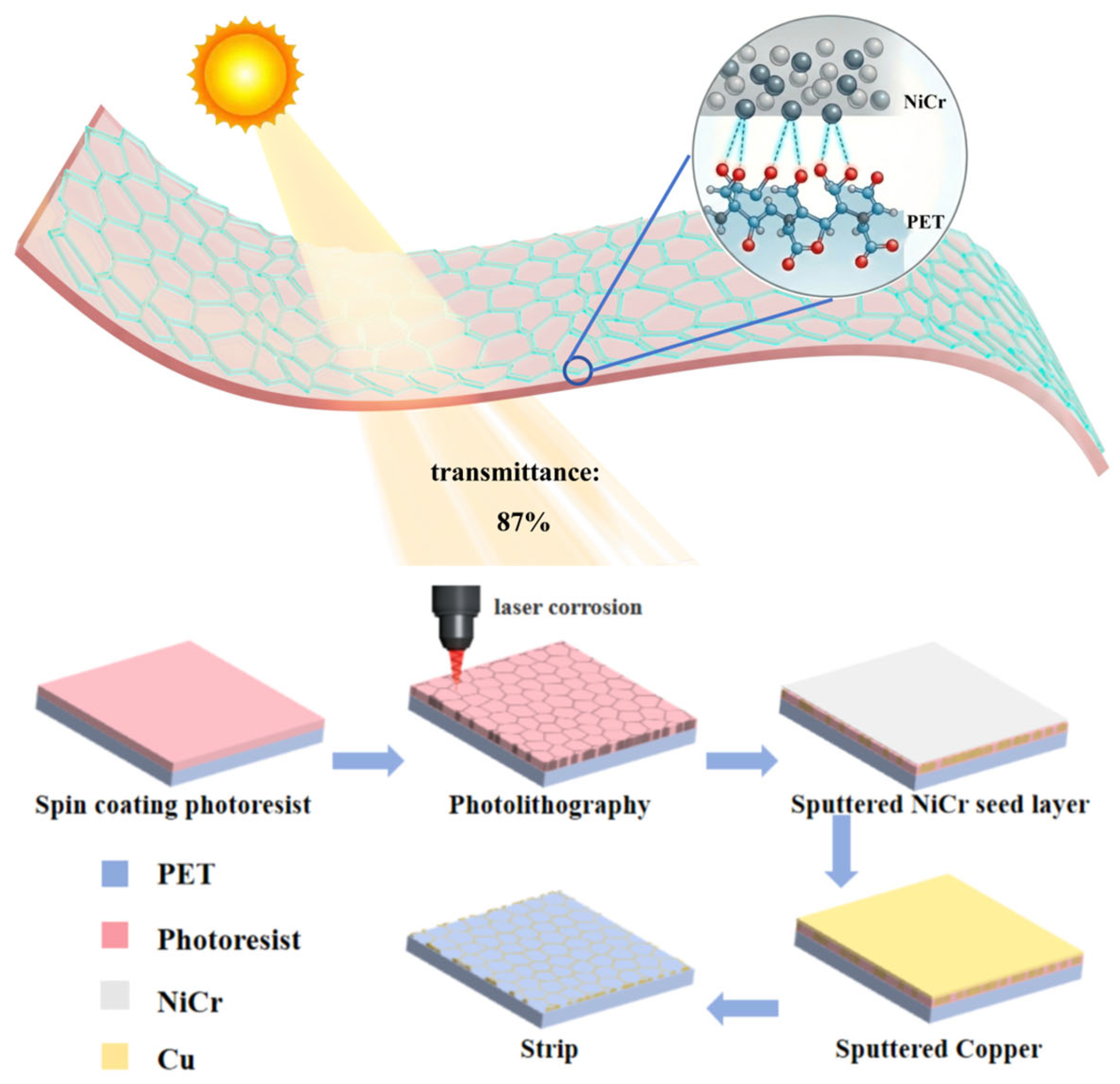
Figure 2.
Interfacial adhesion and microstructural characterization of Cu thin films with different seed layers. (a–c) Optical micrographs of cross-cut tape test results for (a) pristine Cu (seedless), (b) Cu/Al2O3, and (c) Cu/NiCr thin films. (d) Comparison of sheet resistance and electrical resistivity for the three thin film systems. (e) Carrier transport properties (mobility and concentration) derived from Hall effect measurements. (f) XRD patterns. (g–i) 3D-AFM topographic images and corresponding arithmetic average roughness (Ra) values for (g) pristine Cu, (h) Cu/Al2O3, and (i) Cu/NiCr.
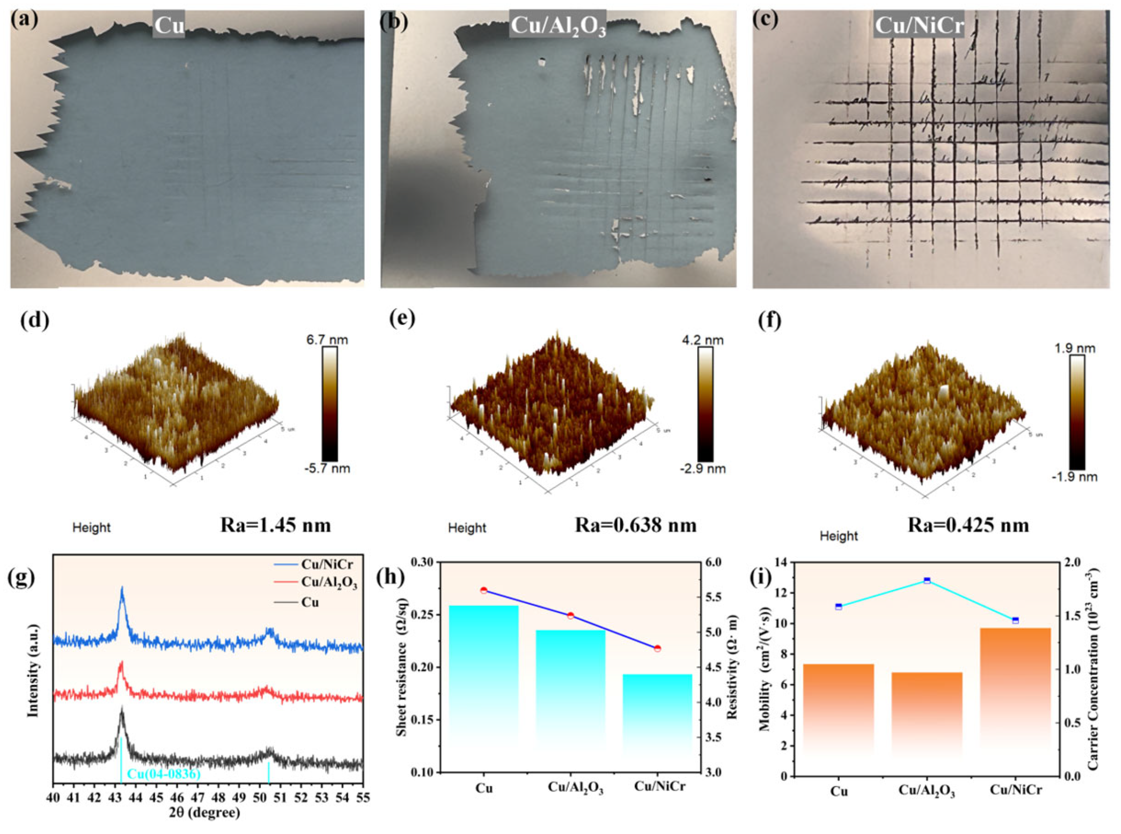
Figure 3.
Elemental composition and interfacial analysis of Cu thin films with Al2O3 and NiCr seed layers. (a–d) STEM-EDS elemental mapping of the Cu/Al2O3 thin film, showing the uniform distribution of Cu (a), Al (b), and O (c) elements, with a merged map (d) confirming the integrity of the oxide seed layer. (e–h) STEM-EDS elemental mapping of the Cu/NiCr thin film, displaying the distribution of Cu (e), Cr (f), and Ni (g) elements, with a merged map (h) verifying Ni/Cr interdiffusion at the Cu-NiCr interface. (i,j) Corresponding EDS spectra quantitatively determining the weight percentages of constituent elements for (i) Cu/Al2O3 and (j) Cu/NiCr samples.
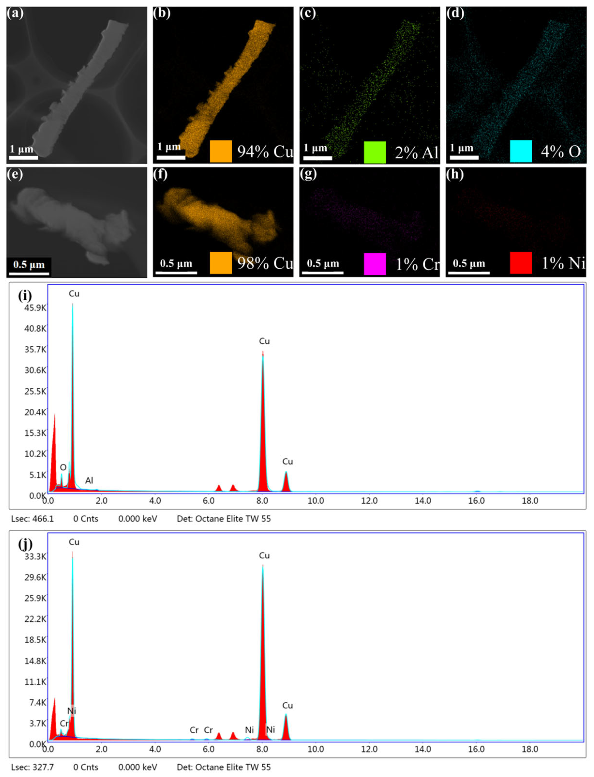
Figure 4.
Electromechanical reliability of Cu thin films under dynamic bending deformation. (a–c) FE-SEM images of as-deposited (a) pristine Cu, (b) Cu/Al2O3, and (c) Cu/NiCr thin films. (d) Schematic of the dynamic bending test setup: bending radius (R) = 2 mm, bending angle (θ) = 60°, and cyclic deformation up to 1000 cycles. (e) Normalized resistance change (R/R0) as a function of bending cycles. (f) Evolution of Hall mobility during bending tests. (g–i) Post-bending FE-SEM images after 1000 cycles: (g) pristine Cu with visible cracks and delamination, (h) Cu/Al2O3 with dense transverse microcracks, and (i) Cu/NiCr retaining a continuous, crack-free surface.
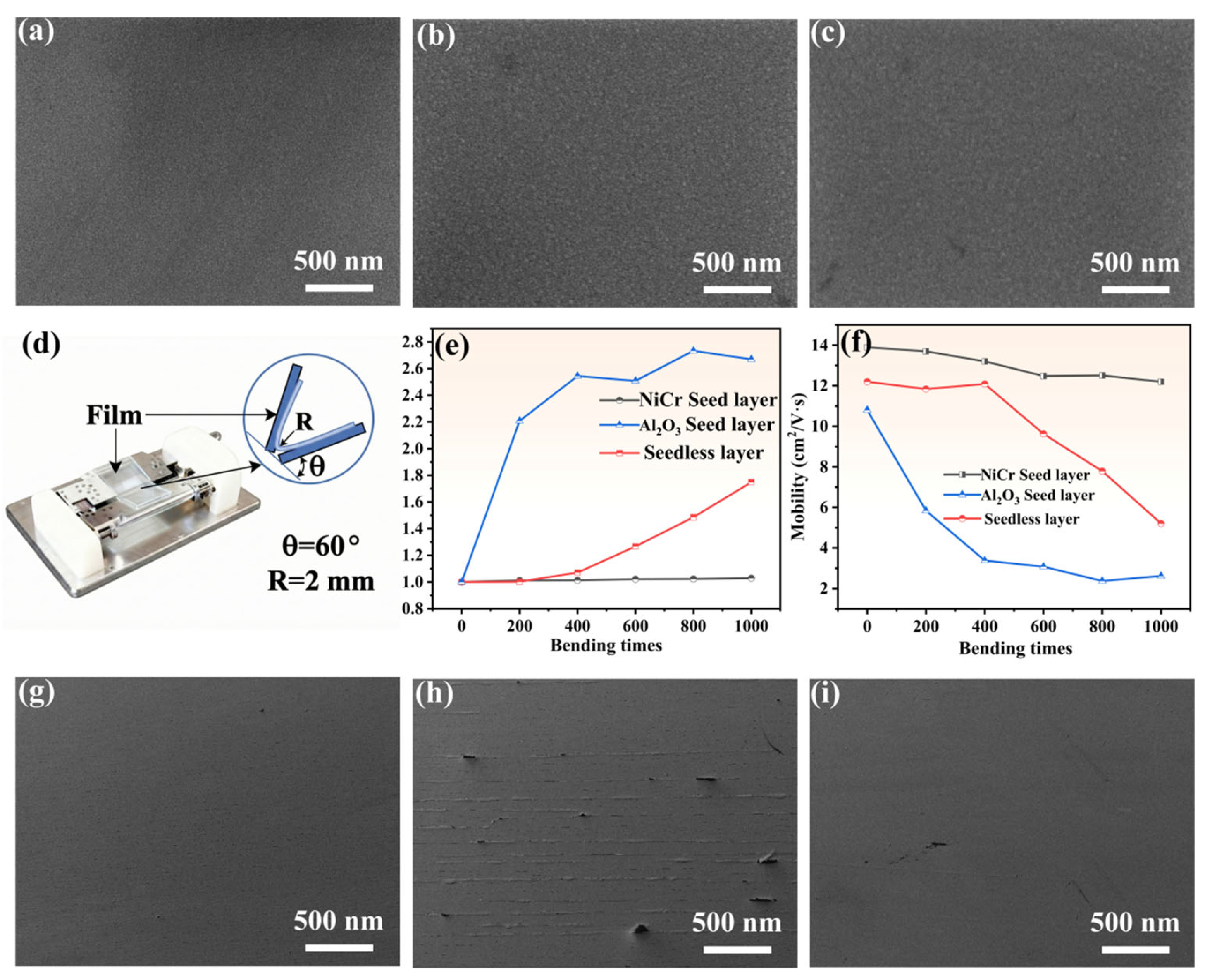
Figure 5.
Environmental stability of Cu thin films under damp-heat aging conditions (85 °C/85% relative humidity, RH). (a–c) Macroscopic optical images of (a) pristine Cu, (b) Cu/NiCr, and (c) Cu/Al2O3 thin films recorded at 0, 40, 80, and 120 min of aging. (d) Sheet resistance and (e) normalized resistance (R/R0) variations as a function of aging time, with the Cu/NiCr thin film exhibiting the highest stability. (f–h) Post-aging 3D AFM images and roughness (Ra) analysis: (f) pristine Cu (Ra = 3.94 nm), (g) Cu/Al2O3 (Ra = 4.45 nm), and (h) Cu/NiCr (Ra = 1.55 nm).
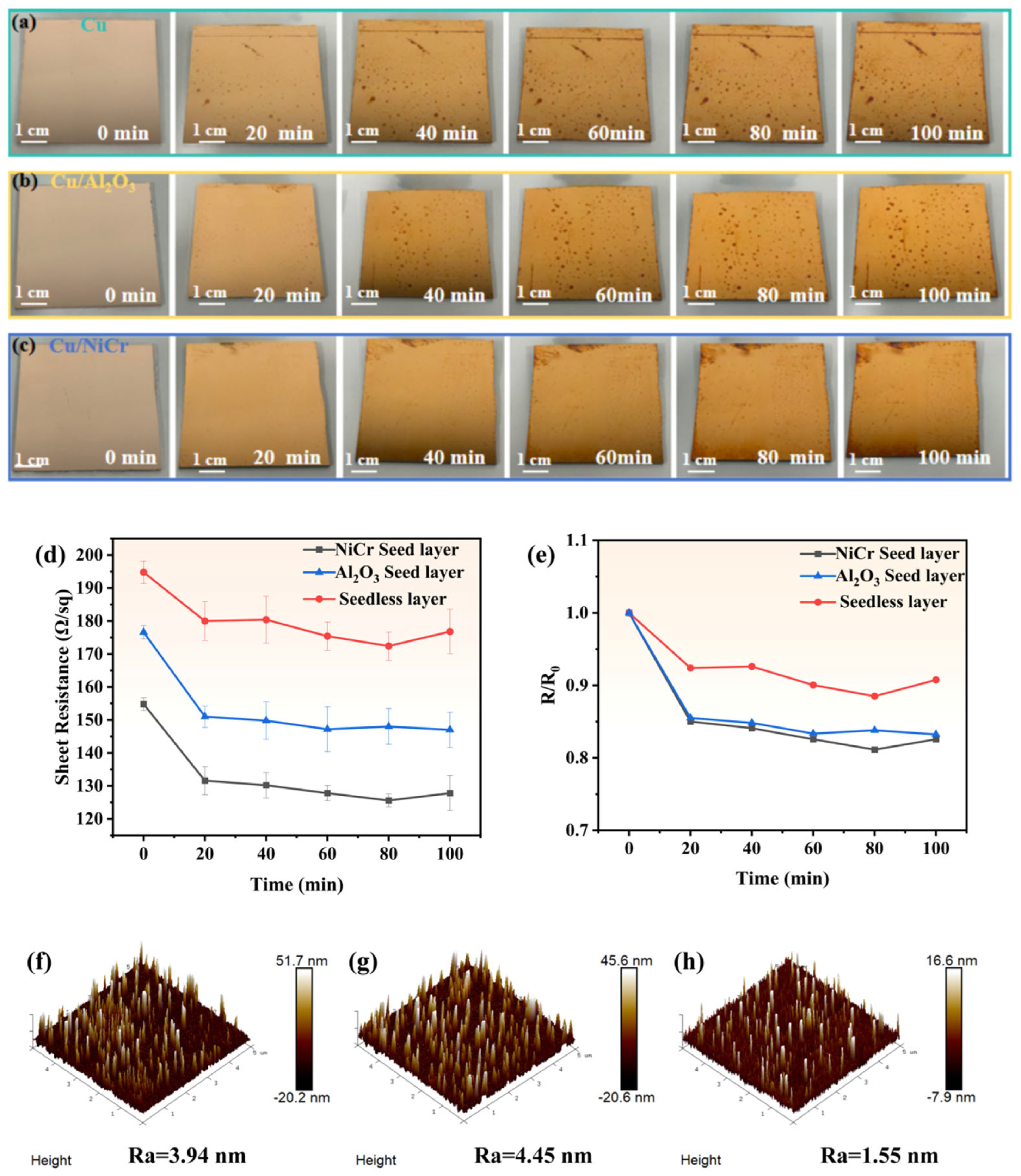
Figure 6.
Geometric engineering of aperiodic Cu meshes for optimized electromechanical performance. (a,b) Metallographic micrographs of (a) Linear and (b) Sinusoidal aperiodic mesh patterns. (c) Digital photograph of the Sinusoidal mesh electrode on a complex background. (d) UV-vis-NIR transmittance spectra of bare PET, Linear, and Sinusoidal thin films in the 400–1000 nm wavelength range. (e) Comparison of sheet resistance and transmittance at 550 nm for the two mesh geometries. (f) Calculated Figure of Merit (FoM) highlighting the superior optoelectronic balance of the Sinusoidal mesh. (g) Normalized resistance change (R/R0) as a function of bending cycles (R = 2 mm). (h,i) Post-bending metallographic micrographs after 2500 cycles: (h) Linear mesh with severe transverse fractures at hexagonal vertices, and (i) Sinusoidal mesh retaining structural integrity without observable cracks.
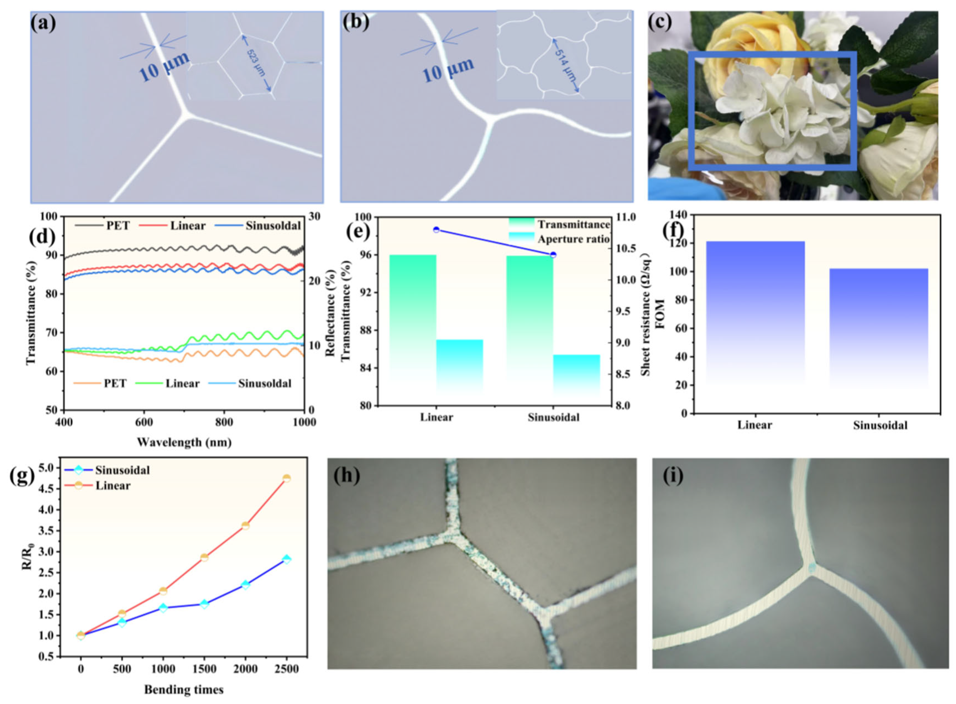
Figure 7.
Performance of flexible transparent heaters (FTHs) based on Linear and Sinusoidal Cu mesh electrodes. (a) Schematic diagram of the FTH device structure: Cu mesh electrode on PET, with copper foil current collectors attached to opposite edges. (b) Time-dependent temperature profiles under a constant applied voltage of 5 V. (c) Temperature response curves under stepwise voltage increases (3 V to 7 V). (d) Long-term operational stability test at 5 V for 20 h.
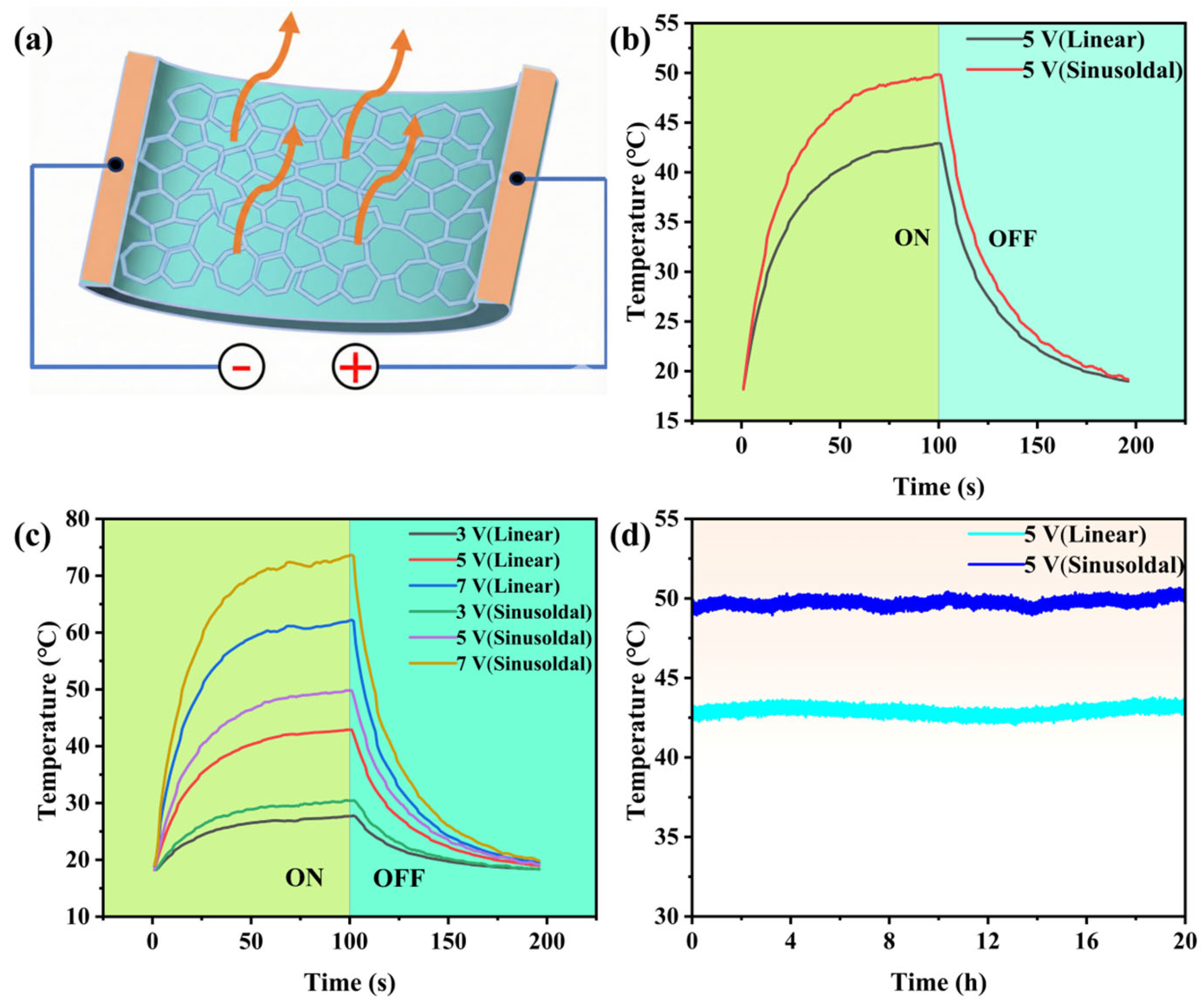

Table 1.
Optoelectronic properties and FoM of Cu mesh electrodes with different geometric parameters.
Table 1.
Optoelectronic properties and FoM of Cu mesh electrodes with different geometric parameters.
| Sample | Rs (Ω/sq) | T (550 nm) (%) | Aperture Ratio | |
|---|---|---|---|---|
| Linear | 10.8 | 87.0 | 96% | 121.3 |
| Sinusoidal | 10.4 | 85.7 | 95.9% | 102.1 |
Disclaimer/Publisher’s Note: The statements, opinions and data contained in all publications are solely those of the individual author(s) and contributor(s) and not of MDPI and/or the editor(s). MDPI and/or the editor(s) disclaim responsibility for any injury to people or property resulting from any ideas, methods, instructions or products referred to in the content. |
© 2026 by the authors. Licensee MDPI, Basel, Switzerland. This article is an open access article distributed under the terms and conditions of the Creative Commons Attribution (CC BY) license (http://creativecommons.org/licenses/by/4.0/).
Copyright: This open access article is published under a Creative Commons CC BY 4.0 license, which permit the free download, distribution, and reuse, provided that the author and preprint are cited in any reuse.


