Submitted:
05 February 2026
Posted:
09 February 2026
You are already at the latest version
Abstract
On-chip integration of two-dimensional (2D) materials provides a promising route for implementing nonlinear integrated photonic devices that break existing barriers and unlock new capabilities. Although 2D materials with ultrahigh optical nonlinearity have driven this technological progress, their high optical absorption also constitutes an Achilles’ heel. Whether 2D materials can overcome their intrinsic absorption and generate net gain (NG) via optical parametric amplification (OPA) processes is a critical and intriguing question, which is central to many nonlinear optical applications. Recently [1], we experimentally demonstrated enhanced OPA and achieved NG in silicon nitride waveguides integrated with 2D graphene oxide (GO) under pulsed pumping. Based on material parameters from this work, this perspective systematically analyzes the feasibility of achieving NG in more widely used, yet more challenging, scenarios involving silicon waveguides incorporating GO and continuous-wave pumping. The results show that a gap still exists toward achieving this goal, but it can be bridged through combined efforts in optimizing waveguide structure, reducing loss of GO, and improving GO’s thermal stability. We also investigate different waveguide structures as well as other 2D materials, and analyze the gap in each case. This work provides a critical roadmap and useful guidance for future developments towards achieving NG via OPA in integrated photonic devices incorporating 2D materials.
Keywords:
integrated optics
; 2D materials
; optical parametric amplification
1. Introduction
Nonlinear integrated photonic devices, which enable all-optical signal generation and processing without inefficient optical-electrical-optical (OEO) conversion, offer far superior processing speed and energy efficiency compared to electronic devices, along with added benefits such as compact device footprint, low power consumption, high stability, and mass production [1,2,3]. Silicon platform that leverages the well-developed complementary metal-oxide-semiconductor (CMOS) fabrication technologies from integrated circuit industry has been a leading platform for integrated photonic devices [2]. Nevertheless, the absence of χ(2) optical nonlinearity and the strong two-photon absorption (TPA) at near-infrared telecommunication wavelengths significantly limit the use of silicon devices for many nonlinear optical applications [4,5]. Although other CMOS compatible platforms, such as silicon nitride (SiN) and doped silica, exhibit much weaker TPA [6,7], they also suffer from limited nonlinear conversion efficiency due to their much lower χ(3) optical nonlinearity compared with silicon.
The era of big data has witnessed an unprecedented surge in data generation and processing, leading to an explosive demand for higher processing speed and energy efficiency in data centers that bear the brunt of this growth. This has driven the pursuit for high-performance nonlinear integrated photonic devices, motivating the hybrid integration of advanced nonlinear optical materials to overcome the limitations of existing integrated platforms [8,9,10]. Since the ground-breaking discovery of graphene in 2004 [11], 2D materials with atomic thickness and extraordinary properties have emerged at the forefront of global research, providing vast opportunities for both fundamental science and industrial applications [12,13,14,15]. In recent years, significant progress has been made in on-chip integration of 2D materials to implement hybrid devices that surpass the performance limits of conventional counterparts and unlock new capabilities [16,17,18]. A substantial body of research has demonstrated the enhancement of fundamental nonlinear optical processes, such as four-wave mixing (FWM) and self-phase modulation (SPM), in hybrid integrated photonic devices incorporating 2D materials [19,20]. Although the ultrahigh optical nonlinearity of 2D materials has been widely recognized, their considerably higher light absorption compared with conventional bulk integrated materials limits their use in many advanced nonlinear optical applications, particularly optical parametric amplification (OPA) [21,22,23] and optical micro-comb generation based on OPA [24,25,26]. As illustrated in Figure 1, in these applications critical questions arise as to whether the high parametric gain (PG) provided by 2D materials with high optical nonlinearity can compensate for their high loss to achieve net gain (NG), and how close current technologies are to realizing this goal. These issues are fundamental and of broad interest to the related research community, yet remain unaddressed.
Recently [1], we experimentally demonstrated NG of up to ~24 dB for femtosecond optical pulses propagating through SiN waveguides integrated with 2D graphene oxide (GO) films, representing the first demonstration of achieving NG via OPA by integrating 2D materials onto photonic chips. In this perspective, based on practical material parameters obtained from this work, we systematically analyze the feasibility of achieving NG via OPA in silicon waveguides incorporating GO and using continuous-wave (CW) light. This is highly challenging due to the strong TPA of silicon at telecommunication wavelengths and the much lower peak power of CW light compared with optical pulses. Nevertheless, it is of great significance given silicon’s dominant role in integrated photonic devices and the more widely use of CW pumping for nonlinear optical applications. Our simulation results reveal that although a gap remains toward achieving this goal, it can be bridged through coordinated advances in optimizing waveguide structure, reducing loss of GO, and improving GO’s thermal stability. We also investigate and analyze the existing gap for different types of silicon waveguides including nanowire waveguides, rib waveguides, etchless waveguides, and slot waveguides, as well as for other 2D materials such as graphene and molybdenum disulfide (MoS2). This work presents a clear roadmap and practical insights to guide future efforts towards achieving NG via OPA in integrated photonic devices incorporating 2D materials.
2. Limitations for Achieving NG via OPA in Bulk Integrated Photonic Devices
OPA underpins many modern optical applications, such as optical communications, broadband optical sources, and optical micro-comb generation [21,23]. Compared with optical amplifiers based on rare-earth-doped fibers and III-V semiconductors, OPA-based amplifiers can offer gain over much broader wavelength ranges and enable optical amplification using passive devices [22,23]. In this section, we discuss the limitations of conventional SiN and silicon waveguides in achieving NG via OPA at telecommunication wavelengths (centered at 1550 nm). Based on the theory detailed in Note 1 of Supplementary information (SI), we performed simulation using typical material parameters and waveguide loss factors aligned with state-of-the-art fabrication capabilities. Our discussion of OPA in this paper focuses on that based on χ(3) optical nonlinearity, although we note that OPA can also be induced by χ(2) optical nonlinearity [27,28,29].
In Figure 2, we analyze the PG for SiN waveguides. Note that the PG values here and in our following discussion refer to net parametric gain over and above the intrinsic loss of the waveguides (i.e., achieving NG requires PG > 0). This differs from the “on/off parametric gain” quoted in Refs. [30,31], where the waveguide loss is excluded, resulting in higher PG values.
To simplify the discussion, our PG simulation here and in the following analysis assume that the signal and pump wavelengths are closely spaced, so that the phase mismatch can be neglected.
Figure 2(a) shows the waveguide schematic and transverse-electric (TE) mode profile (at 1550 nm), where the SiN waveguide has a typical cross-section of 1600 nm × 720 nm [1,32]. In our following discussion, we focus on investigating the PG for TE modes as they are more widely used than transverse-magnetic (TM) modes for nonlinear integrated photonic devices, particularly those incorporating 2D materials [9,33,34].
Figure 2(b) shows the simulated PG for the SiN waveguide in Figure 2(a) excited by using a CW pump. In our simulation, we used typical waveguide nonlinear parameter (γ = ~1.1 W-1m-1) and dispersion reported in Refs. [1,32]. The typical optical bandgap of SiN is ~5.0 eV, far exceeding twice the photon energy at 1550 nm (i.e., ~1.6 eV) and resulting in negligible TPA at telecommunication wavelengths. The waveguide propagation loss (PL) is a critical factor affecting the PG. For comparison, we used two different values for the PL of the SiN waveguides in our simulation. The first one is ~0.5 dB/cm, which is typical for SiN waveguides fabricated with current average fabrication capabilities [1,35]. The second one is ~0.02 dB/cm, corresponding to state-of-the-art fabrication capabilities according to Refs. [22,36]. In Figure 2(b), the white dashed lines denote the condition of PG = 0, and the black points and asterisks mark the results simulated using the parameters of practical devices reported in Refs. [1] and [22], respectively. In Figure 2(b-i), the simulated PG values show good agreement with the experimental results in Refs. [1,22], confirming the accuracy of our simulation. At a pump power of PCW = 2 W, the PG remains negative for waveguide length L ≤ 200 cm when PL = 0.5 dB/cm. In contrast, NG is achievable for 20 cm ≤ L ≤ 200 cm when PL = 0.02 dB/cm. This highlights the significance of reducing the waveguide PL in achieving NG, which is also reflected by the results in Figure 2(b-ii) and 2(b-iii).
Figure 2(c) shows the corresponding results under pulsed pumping, which is based on FWM between a CW light as the signal and optical pulses as the pump ‒ consistent with our experimental demonstration in Ref. [1]. Compared with CW pumping, pulsed pumping enables high peak powers while maintaining low average powers, which helps suppress the material property changes induced by thermo-optic effects. This is particularly important for 2D materials such as GO, which can be reduced at high temperatures [37]. In our simulation, we used optical pulses with a pulse width of 180 fs and a maximum peak power Ppulse of 180 W ‒ consistent with the pulse parameters employed in our previous experiments [1,38]. As can be seen, NG can be easily achieved even for PL = 0.5 dB/cm, and it becomes more significant for PL = 0.02 dB/cm. This is mainly because the high peak power of the pumping pulses significantly enhances the efficiency of the OPA process. It should be noted that the PG values shown inFigure 2(c) and in the following pulsed pumping analysis correspond to the maximum values achieved at the peak powers, which cannot be sustained over long times due to the short pulse duration.
Following the analysis performed for SiN waveguides, the corresponding results for silicon nanowire waveguides are provided in Figure 3. In our simulation, the silicon nanowire waveguides have a typical cross-section of 450 nm × 220 nm, and we used typical waveguide nonlinear parameter (γ = ~288 W-1m-1) and dispersion reported in Ref. [20]. Compared with SiN waveguides, the nonlinear parameter of silicon nanowire waveguide is two orders of magnitude larger ‒ owing to silicon’s much higher Kerr coefficient (~6.0 × 10⁻¹⁸ m2/W [20,39]) relative to SiN (~2.6 × 10⁻¹⁹ m2/W [32]) and the much smaller effective mode area. Unlike SiN with a large bandgap that yields negligible TPA at telecommunication wavelengths, the much smaller optical bandgap of silicon (~1.12 eV [2,40]) leads to significant TPA in this range. The nonlinear optical absorption induced by TPA, as well as parasitic free-carrier effects (i.e., free carrier dispersion and free carrier absorption [2]) were considered in our simulation for silicon devices (see details in Note 2 of SI).
Similar to that in Figure 2, we used two different values for the PL of the silicon nanowire waveguides in our simulation: 4.3 dB/cm representing average fabrication capabilities [20] and 1.0 dB/cm corresponding to state-of-the-art fabrication capabilities [41]. We performed simulation for both CW and pulsed pumping, and in both cases, the PG remains negative within the investigated power and waveguide length ranges. This is mainly due to the strong TPA that induces significant nonlinear optical loss that increases with input power, highlighting the challenges of achieving NG in silicon waveguides. We note that Ref. [30] reported achieving NG in silicon nanowire waveguides with a cross-section of 600 nm × 300 nm, so we also performed simulation for this waveguide geometry. The simulation results show that achieving NG remains challenging in this case when TPA is taken into account (see details in Note 3 of SI). In fact, the results in Ref. [30] were achieved based on FWM between two synchronized picosecond optical pulses, for which the TPA-induced free carrier effects can be neglected since the generated free carriers with long life times (typically on the order of ~1 ns [42,43]) do not have sufficient time to recombine within the pulse duration. This differs from FWM between two CW lights or between a CW light and a pulsed pump, as discussed in Figure 2(c) and 3(c), where TPA induced free carrier effects are no longer negligible.
In Figure 4 and Figure 5, we analyze the PG for other types of silicon waveguides including rib, etchless, slab, and slot waveguides. Each of these waveguides has its own characteristics and has been widely studied and employed in diverse applications [44,45,46].
Figure 4 shows the results for silicon rib, etchless, and slab waveguides that exhibit lower PL than nanowire waveguides. In Figure 4(a), the rib waveguides have a cross-section of 1000 nm × 380 nm, and the cap has an etched depth of 70 nm. The rib waveguides with a shallow-etched structure exhibit weaker optical confinement, which reduce mode overlap with scattering sidewalls and consequently lower the PL [47]. In Figure 4(b), the etchless waveguides have a cross-section of 1000 nm× 70 nm. These waveguides can be fabricated by first growing and patterning a thermal oxide mask, followed by defining the waveguide core through thermal oxidation of silicon, where the silicon layer remains completely free from the etching process, resulting in extremely smooth silicon/silica interface and significantly reduced PL [48]. In Figure 4(c), the slab waveguides have a cross-section of 900 nm × 60 nm. The low PL is enabled by the ultra-thin waveguide structure that exhibits lower sensitivity to sidewall roughness [49]. In our simulation, the PL values of the silicon rib, etchless, and slab waveguides were 0.4, 0.3, and 0.6 dB/cm, respectively. These values were consistent with those reported in Refs. [47,48,49]. The corresponding nonlinear parameters of these waveguides were ~30, ~89, and ~69 W-1m-1, respectively, calculated using the same n2 of silicon for the nanowire waveguide but with effective mode areas specific to each waveguide configuration. As can be seen, although these waveguides offer lower PL values compared with nanowire waveguides, this comes at the expense of lower optical nonlinearities. Similar to the results in Figure 3, for both CW and pulsed pumping, the PG remains negative within the power and waveguide length ranges investigated in Figure 4. This further highlights the challenges of overcoming the TPA of silicon and achieving NG in silicon waveguides at telecommunication wavelengths.
Figure 5 shows the simulation results for silicon slot waveguides. Owing to their ability to confine light tightly within nanoscale slot regions, slot waveguides offer exceptionally strong field confinement and greatly enhanced light-matter interaction, making them widely used for optical sensing, nonlinear photonics, and electro-optic modulation [50,51]. We analyze slot waveguides with different slot widths of 100, 150, and 200 nm inFigure 5. Each silicon waveguide on both sides of the slot region has a cross-section of 225 nm × 220 nm. The slot region and the upper cladding are made of silica, and the fabrication of such slot waveguides can be achieved using techniques detailed in Ref. [41]. In our simulation, the PL values of the slot waveguides with 100-nm, 150-nm, and 200-nm slot widths were 4.1, 5.0, and 6.3 dB/cm, respectively ‒ consistent with those reported in Ref. [41]. The calculated nonlinear parameters of these waveguides were ~13, ~8.8, and ~6.4 W-1m-1, respectively. Similar to the results in Figure 3 and Figure 4, the PG remains negative for both CW and pulsed pumping. A key reason is that the material filling the slot region is silica, which has a very low Kerr coefficient (~2.6 × 10⁻²⁰ m2/W [52]). By filling the slot region with highly nonlinear materials such as nonlinear polymers [53] and 2D materials [54], the waveguide optical nonlinearity can be significantly improved, offering a promising route toward achieving NG. Detailed analysis for achieving NG in slot waveguides with highly nonlinear 2D materials is provided in Section 3.
3. Challenges and Opportunities for Achieving NG via OPA in Hybrid Integrated Photonic Devices Incorporating 2D Materials
The limitations for achieving NG via OPA in bulk nonlinear integrated photonic devices motivate on-chip integration of advanced materials to address them. In this section, we systematically analyze the challenges and opportunities for achieving NG via OPA in integrated photonic devices incorporating 2D materials. Our discussion focuses on devices with 2D GO films based on our experimental work in Ref. [1], and comparisons between GO and other 2D materials such as graphene and MoS2 will also be provided.
In Figure 6, we analyze the PG of SiN waveguides coated with 2D monolayer GO films. GO is an oxidized derivative of graphene, featuring carbon networks decorated with diverse oxygen-containing functional groups (OCFGs) such as hydroxyl, carboxyl, and carbonyl groups [14,55]. Among various 2D materials, GO provides several key advantages for OPA applications, including high optical nonlinearity (~1.5 × 10⁻¹⁴ m2/W, which is about 5 orders of magnitude higher than that of SiN [32,38]) and a large optical bandgap (2.1 – 3.6 eV [56]) that yields low linear optical absorption and nonlinear TPA at near-infrared wavelengths. In addition, GO has facile solution-based synthesis processes [57] and transfer-free film coating with precise control over the thickness [58], showing strong capability for large-scale manufacturing and high compatibility with integrated device platforms [10].
Figure 6(a) shows the waveguide schematic and TE mode profile (at 1550 nm). The SiN waveguide structure is the same as that in Figure 2(a), except that the silica upper cladding is removed to enable coating of a GO film on the top surface. InFigure 6(b-i), we investigate the PG versus waveguide length L and CW pump power PCW under current fabrication capabilities [1]. In our simulation, the material property parameters of GO, including refractive index (n = ~1.97 at 1550 nm), extinction coefficient (k =~ 0.012 at 1550 nm), film thickness (~2 nm), and Kerr coefficient (n2 = ~1.5 × 10⁻¹⁴ m2/W) were consistent with those obtained from our experiments in Refs. [1,32]. The calculated nonlinear parameter of the hybrid waveguide and GO-induced excess propagation loss (EPLGO, after excluding PL of the uncoated SiN waveguide) were ~14.5 W-1m-1 and ~3 dB/cm, respectively ‒ both of which are typical of current GO film fabrication capabilities [1,32]. The PL of the uncoated SiN waveguide (~0.2 dB/cm) was estimated according to the state-of-art PL of clad SiN waveguides (~0.02 dB/cm) and the current etching techniques. The asterisk marks the simulated PG that agrees well with the experimental result in Ref. [1]. As can be seen, the PG remains negative within the investigated ranges of waveguide length and pump power. This indicates achieving NG under CW pumping in the GO-SiN hybrid waveguides remains challenging under current fabrication capabilities. Our simulation also shows that the hybrid waveguides exhibit higher PG than comparable SiN waveguides without GO (see details in Note 4 of SI). This reflects the fact that, although incorporating 2D GO does not enable NG, it is still beneficial for improving the OPA performance.
The reduction of GO at high temperatures or under high optical powers, which breaks the chemical bonds between the OCFGs and the carbon network, is an intrinsic feature of GO that can limit its use for high-power OPA applications. As the degree of reduction increases, reduced GO (rGO) exhibits decreased optical bandgaps and increased optical absorption, which can result in decreased PG. InFigure 6(b-i), the dashed-dot line marks the CW pump power threshold (Pthres = ~0.2 W) above which significant GO reduction occurs, according to the experimental results in Ref. [37]. It should be noted that the Pthres is not a fundamental limit and can be further increased (as indicated by the arrow) by improving the thermal stability of GO. For instance, our previous work showed that modifying the degree of oxidation of GO using an electrochemical method allows GO to preserve a high Kerr nonlinearity while significantly enhancing its thermal stability (>100 times) under high-power laser illumination [59].
In addition to thermal stability, there remains room to further reduce the linear loss of 2D GO films and optimize their performance for OPA applications. In principle, GO with a bandgap > 2 eV exhibits negligible linear optical absorption at near infrared wavelengths, and the linear loss of practical GO films is dominated by defect-induced absorption and scattering loss arising from imperfect layer contact and film unevenness [60,61]. As these loss sources are fabrication-dependent and difficult to quantify, estimating the minimum linear loss achievable in practical GO films is challenging. What is clear, however, is that there remains significant room to reduce the EPLGO arising from these sources by optimizing the film fabrication processes. InFigure 6(b-ii), we plot PG of GO-SiN waveguides versus L and EPLGO. In our simulation, the input CW pump power is 0.2 W. For comparison, all the parameters of the hybrid waveguide are the same as those used in Figure 6(b–i), except for the varying EPLGO. The dashed line marks the current loss level of EPLGO = 3 dB/cm (i.e., k = ~ 0.012) [1], and the arrow indicates the desired direction for future optimization. As can be seen, reducing the GO-induced loss alone is still insufficient for achieving NG in the GO-SiN hybrid waveguides.
InFigure 6(b-iii), we further investigate the feasibility of achieving NG through a combined increase in Pthres and decrease in EPLGO, where the PG versus EPLGO and PCW is plotted. The waveguide length in our simulation was L = 2 cm. It can be seen that NG can be achieved with a maximum EPLGO of ~0.5 dB/cm (i.e., k < 0.002) and a minimum PCW of 1 W. This result reveals that maintaining the current level of optical nonlinearity of GO while reducing its extinction coefficient k (by a factor of ~6) and optimizing its thermal stability (> ~5 times), can yield NG under CW pumping in the GO-SiN hybrid waveguides. At PCW = 2 W and EPLGO = 0.1 dB/cm, only a small PG of ~0.2 dB is achieved. We also performed simulation for a longer hybrid waveguide with L = 10 cm (see details in Note 5 of SI), which shows a higher PG of ~4.3 dB at PCW = 2 W and EPLGO = 0.1 dB/cm.
Figure 6(c) shows the corresponding results under pulsed pumping. For comparison, the pulse parameters are consistent with those in Section 2. For pulsed pumping, a low average power can still provide a high peak power (at a low repetition rate) without inducing significant thermal reduction of GO. Therefore, we assume that there are no pump power thresholds in Figure 6(c) and the following analysis on pulsed pumping. Under pulsed pumping, NG can be easily achieved even under the current loss level of EPLGO = 3 dB/cm, together with significant PG enhancement compared to the uncoated SiN waveguides (see details in Note 4 of SI). These results agree with our experimental results in Ref. [1].
Extending the analysis for GO-SiN hybrid waveguides in Figure 6, Figure 7 provides the corresponding results for GO-coated silicon nanowire waveguides. The waveguide structure is the same as that in Figure 3. The self-assembly coating method [58] enables conformal coating of the GO film around the silicon nanowire waveguide. In our simulation, the nonlinear parameter for the GO-silicon hybrid waveguide was 668 W-1m-1 [20], and the PL of the uncoated silicon waveguide was 1.0 dB/cm [41]. Compared GO-SiN waveguides, the stronger GO mode overlap in silicon nanowire waveguides yields a higher nonlinear parameter, and this comes at the expense of a higher EPLGO of ~20 dB/cm) and a lower Pthres of ~0.02 W [39]. As can be seen, even with decreased EPLGO and increased Pthres achievable through fabrication and material optimization, the GO-coated silicon nanowire waveguides remain unable to achieve NG over the investigated CW and pulse pump power ranges. The main limitation for this is still the significant TPA of silicon, and the hybrid waveguides also exhibit higher PG than comparable waveguides without GO (see details in Note 6 of SI).
In Figure 8 and Figure 9, we analyze the PG for other types of silicon waveguides coated with monolayer GO films, including rib, etchless, slab, and slot waveguides as discussed in Figure 4 and Figure 5.Figure 8shows the PG versus EPLGO and pump power for the hybrid rib, etchless, and slab waveguides. For each type of waveguide, the results for both CW and pulsed pumping are provided. To clearly show the evolution of PG, we chose small ranges for the CW (< 1 W) and pulsed (< 20 W) pump powers. We also selected L = 1 mm as an optimized length for achieving NG, and the corresponding results for a longer length of L = 2 cm is provided in Note 7 of SI. Compared to the uncoated waveguides in Figure 4, the incorporation of GO significantly enhances the optical nonlinearity, yielding calculated γ values of ~38, ~1626, and ~1669 W-1m-1, respectively. This enhancement is accompanied by increased excess propagation loss, with calculated EPLGO of ~1.9, ~19.8, and ~20.4 dB/cm based on current GO loss of k = ~0.012. We also calculated Pthres values (only for CW pumping) of the three hybrid waveguides based on the GO mode overlap, which are ~0.05 W, ~0.01 W, and ~0.01 W, respectively.
In Figure 8, the hybrid rib waveguides do not show NG for both CW and pulsed pumping, even with potentially decreased EPLGO and increased Pthres. In contrast, the hybrid etchless and slab waveguides exhibit NG for both CW and pulsed pumping. For CW pumping, NG can be achieved by either reducing EPLGO or increasing PCW. At PCW = 1 W and EPLGO = 5 dB/cm, the PG values for the hybrid etchless and slab waveguides are ~2.0 dB and ~2.7 dB, respectively. For pulsed pumping, NG becomes much easier to achieve and can be realized even with the current GO loss level. In addition, the hybrid slab waveguide exhibits better performance, providing a higher maximum PG value (~4.3 dB) and a broader pulse power range for achieving NG (Ppulse < 13 W) compared with the hybrid etchless waveguide (with a maximum PG of ~3.0 dB and Ppulse < 7 W for achieving NG). The superior performance of the hybrid slab waveguides compared to other types of GO-silicon waveguides highlights the importance of increasing GO mode overlap (to enhance optical nonlinearity) and suppressing silicon mode overlap (to minimize TPA) when optimizing the waveguide structure for achieving high PG.
Figure 9 shows the results for GO-silicon slot waveguides, which have the same waveguide structures as those in Figure 5 except that the slot region is conformally coated with monolayer GO films. The optical nonlinearity of the slot waveguides can be significantly improved by incorporating 2D GO films, showing calculated γ values of ~2517, ~1774, and ~1335 W-1m-1 for the waveguides with 100-nm, 150-nm, and 200-nm slot widths, respectively. The calculated EPLGO were ~59.3, ~51.0, and ~44.9 dB/cm for these waveguides, with corresponding Pthres values of ~0.006 W, ~0.007 W, and ~0.008 W, respectively. Similar to Figure 8, we analyze the PG versus EPLGO and pump power for both CW and pulsed pumping. For CW pumping, the 100-nm and 150-nm slot waveguides can achieve NG at the current GO loss level by increasing Pthres. At PCW = 2 W and with current GO loss of k = ~0.012, a PG of ~0.6 dB can be obtained for the 100-nm slot waveguides. On this basis, a much higher PG of ~6.7 dB could be achieved by reducing the GO loss to k = ~0.003. For the 200-nm slot waveguides with weaker mode confinement, the PG is lower at the same PCW and k, and achieving NG requires a combined decrease in EPLGO and increase in Pthres. For pulsed pumping,
NG can be readily achieved at the current GO loss level when Ppulse is less than ~20 W, ~30 W, and ~40 W for the 100-nm, 150-nm, and 200-nm slot waveguides, respectively. At Ppulse = 10 W and with current GO loss level, the PG values for the three waveguides are ~1.8 dB, ~4.1 dB, and ~5.2 dB, respectively. The 200-nm slot waveguide achieves a higher PG than the 100-nm and 150-nm slot waveguides, showing a trend opposite to the results for CW pumping. This is mainly due to the fact that the much stronger mode confinement in the 100-nm and 150-nm slot waveguides also significantly enhances TPA under pulsed pumping with high peak powers. It is also worth noting that these PG values of the hybrid slot waveguides are higher than comparable values of ~-0.7 dB for the hybrid slab waveguide in Figure 8(c-iii) and ~-15.8 dB for the hybrid nanowire waveguide in Figure 7(c-iii), reflecting that the slot waveguide structure exhibits the best performance for achieving high PG via OPA among all the waveguide structures we investigated.
As mentioned previously, a phase-matched condition is assumed for the simulation in Figure 2Figures –Figure 9. Therefore, the simulated PG values represent the maximum achievable values. Phase mismatch over a large wavelength range degrades the OPA performance, and we have also performed simulations to investigate the influence of phase mismatch on the PG. Detailed results are provided in Note 8 of SI.
In Figure 10, we compare the PG of SiN and silicon waveguides incorporating different 2D materials, including GO discussed previously, as well as graphene and MoS2 as representative examples. For comparison, we performed simulation for the devices incorporating monolayer GO, graphene, MoS2 films with typical thicknesses of ~2 nm [1], ~0.3 nm [62], and ~0.7 nm [63], respectively. Among these three 2D materials, GO with a bandgap of ~2.0 eV ‒3.5 eV exhibits the lowest third-order optical nonlinearity (n2 = ~1.5 × 10⁻¹⁴ m2/W [64]) and the lowest linear optical absorption (k = ~0.012 at ~1550 nm [1]) at the near-infrared wavelengths we investigated. Graphene with zero bandgap exhibits the highest absolute value of third-order optical nonlinearity (n2 = ~-1.0 × 10⁻¹³ m2/W [65]) and the highest linear optical absorption (with k = ~1.35 at ~1550 nm [66]). MoS2 is a representative transition metal dichalcogenide (TMDC) with a direct bandgap of ~1.8 eV ‒ 1.9 eV in the monolayer form, exhibiting moderate third-order optical nonlinearity (n2 = ~2.3 × 10⁻¹⁴ m2/W [67]) and linear optical absorption (k = ~0.1 at ~1550 nm [67]). In our simulation, the nonlinear optical absorption of graphene was taken into account using the nonlinear absorption coefficient of β = 1.0 × 10⁻⁷ m/W reported in Ref. [65]. For GO and MoS2, their nonlinear optical absorption at near infrared wavelengths was not considered given their large optical bandgaps, although we notice that doping or defect states can induce strong nonlinear optical absorption in these materials [34,67].
Figure 10(a-i) shows PG versus pump power for SiN waveguides incorporating the three 2D materials under CW pumping. Except for the coated 2D materials, the SiN waveguides discussed here are the same as those in Figure 6. In our simulation, a relatively short waveguide length of L = 1 mm was chosen to mitigate performance degradation induced by the loss of 2D materials. The simulation of GO was performed based on its current level of linear loss and thermal stability. The calculated nonlinear parameter and graphene-induced excess propagation loss for the graphene-coated SiN waveguide were γ = ~-50 W-1m-1 and EPLgrahene = ~123 dB/cm, respectively. For the MoS2-coated SiN waveguide, these parameters were γ = ~32 W-1m-1 and EPLMoS2 = ~24 dB/cm. As can be seen, none of the three waveguides achieves NG under CW pumping, and the GO hybrid waveguide exhibits the highest PG among them. The latter indicates a better trade-off between enhanced optical nonlinearity and increased loss for the GO hybrid waveguide. Figure 10(a-ii) shows the corresponding results of Figure 10(a-i) under pulsed pumping. As can be seen, all the three waveguides can achieve NG when Ppulse is sufficiently high. The graphene-coated waveguide still exhibits the lowest PG among the three, but the MoS2-coated waveguide achieves higher PG than the GO-coated waveguide when Ppulse > 50 W, reflecting that at high power levels MoS2 exhibits a better trade-off between optical nonlinearity and loss.
In Figure 10(b), we compare the PG of silicon nanowire waveguides incorporating the three 2D materials under both CW and pulsed pumping. Except for the coated 2D materials, the silicon nanowire waveguides are the same as those inFigure 7. The calculated γ and EPLgraphene for the graphene-coated silicon waveguide were ~1146 W-1m-1 and ~516 dB/cm, respectively. For the MoS2-coated silicon waveguide, these parameters were γ = ~1716 W-1m-1 and EPLMoS2 = ~193 dB/cm. These values are much higher than those for the graphene-coated and MoS2-coated SiN waveguides due to the much stronger mode overlap with 2D materials in these waveguides. For CW pumping in Figure 10(b-i), NG is still not achieved in any of the three hybrid waveguides, and the GO hybrid waveguide achieves the highest PG ‒ similar to those observed in Figure 10(a-i). For pulsed pumping in Figure 10(b-ii), none of the three waveguides achieves NG, and the PG decreases as Ppulse increases, exhibiting a trend different from that observed in Figure 10(a-ii). This reflects the fact that the strong TPA of silicon remains dominant in these hybrid waveguides. The GO hybrid waveguide exhibits much higher PG than the other two waveguides under both CW and pulsed pumping, highlighting the smaller gap for GO towards achieving NG and motivating the focus on GO optimization in this work.
Finally, we note that some 2D materials, such as doped graphene and GO with defect states [68,69], exhibit saturable absorption (SA) behavior, featured by a decrease in loss with increasing input power ‒ opposite to that of TPA [10,70]. The decrease in loss enabled by the SA of 2D materials is beneficial for boosting the OPA processes and can be utilized to improve the PG, but it predominantly manifests under pulsed excitation with high peak powers, rather than under CW pumping. Although in this paper we mainly discuss the OPA arising from χ(3) optical nonlinearity, it can also be realized by leveraging χ(2) optical nonlinearity of non-centrosymmetric 2D materials. Recently [29], experimental demonstration of OPA in 2D TMDCs based on their high χ(2) optical nonlinearity has been reported. Owing to the atomic thickness of the TMDCs, the PG was achieved without phase-matching constraints, and the efficiency was independent of the in-plane polarization of the signal and pump lights. Similar to TMDCs, GO exhibits a non-centrosymmetric atomic structure that yields a large χ(2) optical nonlinearity that is absent in undoped graphene with a centrosymmetric atomic structure [71,72]. This property provides opportunities for future OPA applications. It is also worth noting that the family of 2D materials is rapidly growing, and many newly discovered 2D materials with ultrahigh optical nonlinearity are emerging, such as rhenium sulfur (ReS2, a member of TMDCs with a large χ(2) = ~1.0× 10⁻⁹ m/V [73]), gallium selenide (GaSe, a member of IIIA-VIA[76–106 compounds with a large χ(3) = ~1.4 × 10⁻¹⁶ m2/V2 [74]), and bismuth selenide (Bi2Se3, a typical topological insulator with ultra-broad response bandwidth spanning from the visible to the terahertz regions [75]). This work has broad implications for microcombs [76,77,78,79,80,81,82,83,84,85,86,87,88,89,90,91,92,93,94,95,96,97,98,99,100,101,102,103,104,105,106] and their applications to microwave photonics, neuromorphic processors and communications. [107,108,109,110,111,112,113,114,115,116,117,118,119,120,121,122,123,124,125,126,127,128,129,130,131,132,133,134,135,136,137,138,139,140,141,142,143,144,145,146,147,148,149,150,151,152,153,154,155,156,157] The addition and use of 2D materials [158,159,160,161,162,163,164,165,166,167,168,169,170,171,172,173,174,175,176,177,178,179,180,181,182,183,184,185,186,187,188,189,190,191,192,193,194,195,196,197,198,199,200,201,202,203] will add extra functionality to microcomb chips for potential applications to quantum photonics [204,205,206,207,208,209,210,211,212,213,214,215,216,217,218,219] and other areas. [220,221,222,223,224,225,226,227,228,229] As new materials continue to be discovered, this field is expected to see further exciting progress in the future.
4. Conclusions
In this perspective, we discuss the current challenges and future opportunities towards achieving NG via OPA in photonic chips integrated with 2D materials. Based on material parameters obtained from our previous experiments, we systematically analyze the feasibility of achieving NG via OPA in silicon and SiN waveguides incorporating 2D GO films under both CW and pulsed pumping. Our analysis reveals that, although a gap remains in achieving NG with current fabrication capabilities, it is not fundamental and can be bridged through combined efforts in optimizing waveguide structure, reducing loss of GO, and improving GO’s thermal stability. We also compare the performance for different waveguide structures and 2D materials, and analyze the existing gap in each case. Our work provides a roadmap for engineering OPA-induced PG in integrated photonic devices incorporating 2D materials. With continued improvements in fabrication capabilities and optimization of material properties, nonlinear integrated photonic devices incorporating advanced 2D materials are expected to progressively deliver on their high promise in the future.
Supplementary Materials
The following supporting information can be downloaded at website of this paper posted on Preprints.org.
Conflicts of Interest
The authors declare no competing financial interest.
References
- Yang, Q., et al., Integrated optical parametric amplifiers in silicon nitride waveguides incorporated with 2D graphene oxide films. Light: Advanced Manufacturing, 2024. 4(4): p. 437-452.
- Leuthold, J.; Koos, C.; Freude, W. Nonlinear silicon photonics. Nat. Photon- 2010, 4, 535–544. [CrossRef]
- Moss, D.; Morandotti, R.; Gaeta, A.L.; Lipson, M. New CMOS-compatible platforms based on silicon nitride and Hydex for nonlinear optics. Nat. Photonics 2013, 7, 597–607. [CrossRef]
- Griffith, A.G.; Lau, R.K.; Cardenas, J.; Okawachi, Y.; Mohanty, A.; Fain, R.; Lee, Y.H.D.; Yu, M.; Phare, C.T.; Poitras, C.B.; et al. Silicon-chip mid-infrared frequency comb generation. Nat. Commun. 2015, 6, 6299. [CrossRef]
- Lin, Q.; Zhang, J.; Fauchet, P.M.; Agrawal, G.P. Ultrabroadband parametric generation and wavelength conversion in silicon waveguides. Opt. Express 2006, 14, 4786–4799. [CrossRef]
- Levy, J.S.; Gondarenko, A.; Foster, M.A.; Turner-Foster, A.C.; Gaeta, A.L.; Lipson, M. CMOS-compatible multiple-wavelength oscillator for on-chip optical interconnects. Nat. Photon- 2009, 4, 37–40. [CrossRef]
- Ferrera, M.; Razzari, L.; Duchesne, D.; Morandotti, R.; Yang, Z.; Liscidini, M.; Sipe, J.E.; Chu, S.; Little, B.E.; Moss, D.J. Low-power continuous-wave nonlinear optics in doped silica glass integrated waveguide structures. Nat. Photon- 2008, 2, 737–740. [CrossRef]
- Gu, T.; Petrone, N.; McMillan, J.F.; van der Zande, A.; Yu, M.; Lo, G.Q.; Kwong, D.L.; Hone, J.; Wong, C.W. Regenerative oscillation and four-wave mixing in graphene optoelectronics. Nat. Photon- 2012, 6, 554–559. [CrossRef]
- Chen, H.; Corboliou, V.; Solntsev, A.S.; Choi, D.-Y.; A Vincenti, M.; de Ceglia, D.; de Angelis, C.; Lu, Y.; Neshev, D.N. Enhanced second-harmonic generation from two-dimensional MoSe2 on a silicon waveguide. Light. Sci. Appl. 2017, 6, e17060–e17060. [CrossRef]
- Zhang, Y.; Wu, J.; Jia, L.; Qu, Y.; Yang, Y.; Jia, B.; Moss, D.J. Graphene Oxide for Nonlinear Integrated Photonics. Laser Photon- Rev. 2023, 17. [CrossRef]
- Novoselov, K.S.; Geim, A.K.; Morozov, S.V.; Jiang, D.; Zhang, Y.; Dubonos, S.V.; Grigorieva, I.V.; Firsov, A.A. Electric field effect in atomically thin carbon films. Science 2004, 306, 666–669. [CrossRef]
- Zhang, Y.; Wu, J.; Jia, L.; Jin, D.; Jia, B.; Hu, X.; Moss, D.; Gong, Q. Advanced optical polarizers based on 2D materials. npj Nanophotonics 2024, 1, 1–17. [CrossRef]
- Zhang, Y.; Wu, J.; Hu, J.; Jia, L.; Jin, D.; Jia, B.; Hu, X.; Moss, D.J.; Gong, Q. 2D material integrated photonics: Toward industrial manufacturing and commercialization. APL Photon- 2025, 10. [CrossRef]
- Wu, J.; Lin, H.; Moss, D.J.; Loh, K.P.; Jia, B. Graphene oxide for photonics, electronics and optoelectronics. Nat. Rev. Chem. 2023, 7, 162–183. [CrossRef]
- Yu, S.; Wu, X.; Wang, Y.; Guo, X.; Tong, L. 2D Materials for Optical Modulation: Challenges and Opportunities. Adv. Mater. 2017, 29. [CrossRef]
- Wu, J.; Yang, Y.; Qu, Y.; Jia, L.; Zhang, Y.; Xu, X.; Chu, S.T.; Little, B.E.; Morandotti, R.; Jia, B.; et al. 2D Layered Graphene Oxide Films Integrated with Micro-Ring Resonators for Enhanced Nonlinear Optics. Small 2020, 16, 1906563. [CrossRef]
- Liu, N.; Yang, X.; Zhu, Z.; Chen, F.; Zhou, Y.; Xu, J.; Liu, K. Silicon nitride waveguides with directly grown WS2for efficient second-harmonic generation. Nanoscale 2021, 14, 49–54. [CrossRef]
- Pelgrin, V.; Yoon, H.H.; Cassan, E.; Sun, Z. Hybrid integration of 2D materials for on-chip nonlinear photonics. Light. Adv. Manuf. 2023, 4, 168. [CrossRef]
- Yonezu, Y.; Kou, R.; Nishi, H.; Tsuchizawa, T.; Yamada, K.; Aoki, T.; Ishizawa, A.; Matsuda, N. Evaluation of graphene optical nonlinearity with photon-pair generation in graphene-on-silicon waveguides. Opt. Express 2019, 27, 30262–30271. [CrossRef]
- Zhang, Y.; Wu, J.; Yang, Y.; Qu, Y.; Jia, L.; Moein, T.; Jia, B.; Moss, D.J. Enhanced Kerr Nonlinearity and Nonlinear Figure of Merit in Silicon Nanowires Integrated with 2D Graphene Oxide Films. ACS Appl. Mater. Interfaces 2020, 12, 33094–33103. [CrossRef]
- Zhao, P.; Shekhawat, V.; Girardi, M.; He, Z.; Torres-Company, V.; Andrekson, P.A. Ultra-broadband optical amplification using nonlinear integrated waveguides. Nature 2025, 640, 918–923. [CrossRef]
- Riemensberger, J.; Kuznetsov, N.; Liu, J.; He, J.; Wang, R.N.; Kippenberg, T.J. A photonic integrated continuous-travelling-wave parametric amplifier. Nature 2022, 612, 56–61. [CrossRef]
- Kuznetsov, N.; Nardi, A.; Riemensberger, J.; Davydova, A.; Churaev, M.; Seidler, P.; Kippenberg, T.J. An ultra-broadband photonic-chip-based parametric amplifier. Nature 2025, 639, 928–934. [CrossRef]
- Herr, T., M.L. Gorodetsky, and T.J. Kippenberg, Dissipative Kerr solitons in optical microresonators. Nonlinear optical cavity dynamics: from microresonators to fiber lasers, 2016: p. 129-162.
- Yao, B.-C.; Wang, W.-T.; Xie, Z.-D.; Zhou, Q.; Tan, T.; Zhou, H.; Guo, G.-C.; Zhu, S.-N.; Zhu, N.-H.; Wong, C.W. Interdisciplinary advances in microcombs: bridging physics and information technology. eLight 2024, 4, 1–36. [CrossRef]
- Sun, Y., et al., Applications of optical microcombs. Advances in Optics and Photonics, 2023. 15(1): p. 86.
- Heydari, D.; Cătuneanu, M.; Ng, E.; Gray, D.J.; Hamerly, R.; Mishra, J.; Jankowski, M.; Fejer, M.; Jamshidi, K.; Mabuchi, H. Degenerate optical parametric amplification in CMOS silicon. Optica 2023, 10, 430–437. [CrossRef]
- Cerullo, G. and S. De Silvestri, Ultrafast optical parametric amplifiers. Review of scientific instruments, 2003. 74(1): p. 1-18.
- Trovatello, C.; Marini, A.; Xu, X.; Lee, C.; Liu, F.; Curreli, N.; Manzoni, C.; Conte, S.D.; Yao, K.; Ciattoni, A.; et al. Optical parametric amplification by monolayer transition metal dichalcogenides. Nat. Photon- 2020, 15, 6–10. [CrossRef]
- Foster, M.A.; Turner, A.C.; Sharping, J.E.; Schmidt, B.S.; Lipson, M.; Gaeta, A.L. Broad-band optical parametric gain on a silicon photonic chip. Nature 2006, 441, 960–963. [CrossRef]
- Ooi, K.J.A.; Ng, D.K.T.; Wang, T.; Chee, A.K.L.; Ng, S.K.; Wang, Q.; Ang, L.K.; Agarwal, A.M.; Kimerling, L.C.; Tan, D.T.H. Pushing the limits of CMOS optical parametric amplifiers with USRN:Si7N3 above the two-photon absorption edge. Nat. Commun. 2017, 8, 13878. [CrossRef]
- Qu, Y.; Wu, J.; Yang, Y.; Zhang, Y.; Liang, Y.; El Dirani, H.; Crochemore, R.; Demongodin, P.; Sciancalepore, C.; Grillet, C.; et al. Enhanced Four-Wave Mixing in Silicon Nitride Waveguides Integrated with 2D Layered Graphene Oxide Films. Adv. Opt. Mater. 2020, 8. [CrossRef]
- Pelgrin, V.; Yoon, H.H.; Cassan, E.; Sun, Z. Hybrid integration of 2D materials for on-chip nonlinear photonics. Light. Adv. Manuf. 2023, 4, 168. [CrossRef]
- Zhang, Y.; Wu, J.; Qu, Y.; Jia, L.; Jia, B.; Moss, D.J. Optimizing the Kerr Nonlinear Optical Performance of Silicon Waveguides Integrated With 2D Graphene Oxide Films. J. Light. Technol. 2021, 39, 4671–4683. [CrossRef]
- Frigg, A., et al., Optical frequency comb generation with low temperature reactive sputtered silicon nitride waveguides. APL Photonics, 2020. 5(1).
- Liu, J.; Huang, G.; Wang, R.N.; He, J.; Raja, A.S.; Liu, T.; Engelsen, N.J.; Kippenberg, T.J. High-yield, wafer-scale fabrication of ultralow-loss, dispersion-engineered silicon nitride photonic circuits. Nat. Commun. 2021, 12, 1–9. [CrossRef]
- Qu, Y.; Yang, Y.; Wu, J.; Zhang, Y.; Jia, L.; El Dirani, H.; Crochemore, R.; Sciancalepore, C.; Demongodin, P.; Grillet, C.; et al. Photo-Thermal Tuning of Graphene Oxide Coated Integrated Optical Waveguides. Micromachines 2022, 13, 1194. [CrossRef]
- Zhang, Y.; Wu, J.; Yang, Y.; Qu, Y.; El Dirani, H.; Crochemore, R.; Sciancalepore, C.; Demongodin, P.; Grillet, C.; Monat, C.; et al. Enhanced self-phase modulation in silicon nitride waveguides integrated with 2D graphene oxide films. IEEE J. Sel. Top. Quantum Electron. 2022, PP, 1–1. [CrossRef]
- Wu, J.; Zhang, Y.; Hu, J.; Yang, Y.; Jin, D.; Liu, W.; Huang, D.; Jia, B.; Moss, D.J. 2D Graphene Oxide Films Expand Functionality of Photonic Chips. Adv. Mater. 2024, 36, e2403659. [CrossRef]
- Liang, D.; Bowers, J.E. Recent progress in lasers on silicon. Nat. Photon- 2010, 4, 511–517. [CrossRef]
- Debnath, K.; Khokhar, A.Z.; Boden, S.A.; Arimoto, H.; Oo, S.Z.; Chong, H.M.H.; Reed, G.T.; Saito, S. Low-Loss Slot Waveguides with Silicon (111) Surfaces Realized Using Anisotropic Wet Etching. Front. Mater. 2016, 3. [CrossRef]
- Yin, L.; Agrawal, G.P. Impact of two-photon absorption on self-phase modulation in silicon waveguides. Opt. Lett. 2007, 32, 2031–2033. [CrossRef]
- Sang, X., E.-K. Tien, and O. Boyraz, Applications of two photon absorption in silicon. Journal of optoelectronics and advanced materials, 2009. 11(1): p. 15.
- Rickman, A.; Reed, G.; Namavar, F. Silicon-on-insulator optical rib waveguide loss and mode characteristics. J. Light. Technol. 1994, 12, 1771–1776. [CrossRef]
- Griffith, A.G.; Lau, R.K.; Cardenas, J.; Okawachi, Y.; Mohanty, A.; Fain, R.; Lee, Y.H.D.; Yu, M.; Phare, C.T.; Poitras, C.B.; et al. Silicon-chip mid-infrared frequency comb generation. Nat. Commun. 2015, 6, 6299. [CrossRef]
- Wang, X.; Zhou, L.; Li, R.; Xie, J.; Lu, L.; Wu, K.; Chen, J. Continuously tunable ultra-thin silicon waveguide optical delay line. Optica 2017, 4, 507–515. [CrossRef]
- Lardenois, S.; Pascal, D.; Vivien, L.; Cassan, E.; Laval, S.; Orobtchouk, R.; Heitzmann, M.; Bouzaida, N.; Mollard, L. Low-loss submicrometer silicon-on-insulator rib waveguides and corner mirrors. Opt. Lett. 2003, 28, 1150–1152. [CrossRef]
- Cardenas, J.; Poitras, C.B.; Robinson, J.T.; Preston, K.; Chen, L.; Lipson, M. Low loss etchless silicon photonic waveguides. Opt. Express 2009, 17, 4752–4757. [CrossRef]
- Zou, Z.; Zhou, L.; Li, X.; Chen, J. 60-nm-thick basic photonic components and Bragg gratings on the silicon-on-insulator platform. Opt. Express 2015, 23, 20784–20795. [CrossRef]
- Yang, A.H.J.; Moore, S.D.; Schmidt, B.S.; Klug, M.; Lipson, M.; Erickson, D. Optical manipulation of nanoparticles and biomolecules in sub-wavelength slot waveguides. Nature 2009, 457, 71–75. [CrossRef]
- Koos, C.; Vorreau, P.; Vallaitis, T.; Dumon, P.; Bogaerts, W.; Baets, R.; Esembeson, B.; Biaggio, I.; Michinobu, T.; Diederich, F.; et al. All-optical high-speed signal processing with silicon–organic hybrid slot waveguides. Nat. Photon- 2009, 3, 216–219. [CrossRef]
- Ranka, J.K.; Windeler, R.S.; Stentz, A.J. Optical properties of high-delta air–silica microstructure optical fibers. Opt. Lett. 2000, 25, 796–798. [CrossRef]
- Baehr-Jones, T.; Penkov, B.; Huang, J.; Sullivan, P.; Davies, J.; Takayesu, J.; Luo, J.; Kim, T.-D.; Dalton, L.; Jen, A.; et al. Nonlinear polymer-clad silicon slot waveguide modulator with a half wave voltage of 0.25V. p. 163303.
- Wang, J.; Cheng, Z.; Chen, Z.; Wan, X.; Zhu, B.; Tsang, H.K.; Shu, C.; Xu, J. High-responsivity graphene-on-silicon slot waveguide photodetectors. Nanoscale 2016, 8, 13206–13211. [CrossRef]
- Wu, J.; Jia, L.; Zhang, Y.; Qu, Y.; Jia, B.; Moss, D.J. Graphene Oxide for Integrated Photonics and Flat Optics. Adv. Mater. 2020, 33, e2006415. [CrossRef]
- Loh, K.P.; Bao, Q.; Eda, G.; Chhowalla, M. Graphene oxide as a chemically tunable platform for optical applications. Nat. Chem. 2010, 2, 1015–1024. [CrossRef]
- Chen, J.; Yao, B.; Li, C.; Shi, G. An improved Hummers method for eco-friendly synthesis of graphene oxide. Carbon 2013, 64, 225–229. [CrossRef]
- Yang, Y.; Lin, H.; Zhang, B.Y.; Zhang, Y.; Zheng, X.; Yu, A.; Hong, M.; Jia, B. Graphene-Based Multilayered Metamaterials with Phototunable Architecture for on-Chip Photonic Devices. ACS Photon- 2019, 6, 1033–1040. [CrossRef]
- Ren, J.; Zheng, X.; Tian, Z.; Li, D.; Wang, P.; Jia, B. Giant third-order nonlinearity from low-loss electrochemical graphene oxide film with a high power stability. p. 221105.
- Wu, J.; Yang, Y.; Qu, Y.; Xu, X.; Liang, Y.; Chu, S.T.; Little, B.E.; Morandotti, R.; Jia, B.; Moss, D.J. Graphene Oxide Waveguide and Micro-Ring Resonator Polarizers. Laser Photon- Rev. 2019, 13, 1900056. [CrossRef]
- Cote, L.J.; Kim, J.; Zhang, Z.; Sun, C.; Huang, J. Tunable assembly of graphene oxide surfactant sheets: wrinkles, overlaps and impacts on thin film properties. Soft Matter 2010, 6, 6096–6101. [CrossRef]
- Demongodin, P.; El Dirani, H.; Lhuillier, J.; Crochemore, R.; Kemiche, M.; Wood, T.; Callard, S.; Rojo-Romeo, P.; Sciancalepore, C.; Grillet, C.; et al. Ultrafast saturable absorption dynamics in hybrid graphene/Si3N4 waveguides. p. 076102.
- Abidi, I.H.; Giridhar, S.P.; Tollerud, J.O.; Limb, J.; Waqar, M.; Mazumder, A.; Mayes, E.L.; Murdoch, B.J.; Xu, C.; Bhoriya, A.; et al. Oxygen Driven Defect Engineering of Monolayer MoS2 for Tunable Electronic, Optoelectronic, and Electrochemical Devices. Adv. Funct. Mater. 2024, 34. [CrossRef]
- Yang, Y.; Wu, J.; Xu, X.; Liang, Y.; Chu, S.T.; Little, B.E.; Morandotti, R.; Jia, B.; Moss, D.J. Invited Article: Enhanced four-wave mixing in waveguides integrated with graphene oxide. p. 120803.
- Ishizawa, A.; Kou, R.; Goto, T.; Tsuchizawa, T.; Matsuda, N.; Hitachi, K.; Nishikawa, T.; Yamada, K.; Sogawa, T.; Gotoh, H. Optical nonlinearity enhancement with graphene-decorated silicon waveguides. Sci. Rep. 2017, 7, 45520. [CrossRef]
- Jia, L.; Wu, J.; Zhang, Y.; Qu, Y.; Jia, B.; Chen, Z.; Moss, D.J. Fabrication Technologies for the On-Chip Integration of 2D Materials. Small Methods 2022, 6, 2101435. [CrossRef]
- Shahaz S. Hameed, D.J., Aihao Zhao, Jiayang Wu *, Irfan H. Abidi *, Junkai Hu, Sebastien Cueff, Christian Grillet, Yuning Zhang, Houssein El Dirani, Corrado Sciancalepore, Sebastien Kerdiles, Quentin Wilmart, Sumeet Walia *, Christelle Monat *, and David J. Moss, . Advanced Materials Technology, 2026.
- Lee, C.-C.; Miller, J.M.; Schibli, T.R. Doping-induced changes in the saturable absorption of monolayer graphene. Appl. Phys. B Laser Opt. 2012, 108, 129–135. [CrossRef]
- Sobon, G.; Sotor, J.; Jagiello, J.; Kozinski, R.; Zdrojek, M.; Holdynski, M.; Paletko, P.; Boguslawski, J.; Lipinska, L.; Abramski, K.M. Graphene Oxide vs Reduced Graphene Oxide as saturable absorbers for Er-doped passively mode-locked fiber laser. Opt. Express 2012, 20, 19463–19473. [CrossRef]
- Liu, Z.; Zhang, X.; Yan, X.; Chen, Y.; Tian, J. Nonlinear optical properties of graphene-based materials. Chin. Sci. Bull. 2012, 57, 2971–2982. [CrossRef]
- Russier-Antoine, I.; Fakhouri, H.; Basu, S.; Bertorelle, F.; Dugourd, P.; Brevet, P.-F.; Velayudhan, P.; Thomas, S.; Kalarikkal, N.; Antoine, R. Second harmonic scattering from mass characterized 2D graphene oxide sheets. Chem. Commun. 2020, 56, 3859–3862. [CrossRef]
- E Fernandes, G.; Kim, J.H.; Osgood, R.; Xu, J.M. Field-controllable second harmonic generation at a graphene oxide heterointerface. Nanotechnology 2018, 29, 105201. [CrossRef]
- Song, Y.; Hu, S.; Lin, M.-L.; Gan, X.; Tan, P.-H.; Zhao, J. Extraordinary Second Harmonic Generation in ReS2 Atomic Crystals. ACS Photon- 2018, 5, 3485–3491. [CrossRef]
- Song, Q.; Zhang, B.; Wang, G. THz absorption spectrum employed for characterize the mixed Gallium selenide-Tin disulfide saturable absorber and its application for passively Q-switched solid state laser. Infrared Phys. Technol. 2018, 93, 87–90. [CrossRef]
- Tielrooij, K.-J.; Principi, A.; Reig, D.S.; Block, A.; Varghese, S.; Schreyeck, S.; Brunner, K.; Karczewski, G.; Ilyakov, I.; Ponomaryov, O.; et al. Milliwatt terahertz harmonic generation from topological insulator metamaterials. Light. Sci. Appl. 2022, 11, 1–8. [CrossRef]
- Moss, D.; Morandotti, R.; Gaeta, A.L.; Lipson, M. New CMOS-compatible platforms based on silicon nitride and Hydex for nonlinear optics. Nat. Photonics 2013, 7, 597–607. [CrossRef]
- Razzari, L.; Duchesne, D.; Ferrera, M.; Morandotti, R.; Chu, S.; Little, B.E.; Moss, D.J. CMOS-compatible integrated optical hyper-parametric oscillator. Nat. Photon- 2009, 4, 41–45. [CrossRef]
- Pasquazi, A.; Peccianti, M.; Park, Y.; Little, B.E.; Chu, S.T.; Morandotti, R.; Azaña, J.; Moss, D.J. Sub-picosecond phase-sensitive optical pulse characterization on a chip. Nat. Photon- 2011, 5, 618–623. [CrossRef]
- M Ferrera et al., “On-Chip ultra-fast 1st and 2nd order CMOS compatible all-optical integration”, Optics Express vol. 19 (23), 23153-23161 (2011).
- Bao, C.; Xuan, Y.; Jaramillo-Villegas, J.A.; Leaird, D.E.; Qi, M.; Weiner, A.M. Direct soliton generation in microresonators. Opt. Lett. 2017, 42, 2519–2522. [CrossRef]
- M.Ferrera et al., “CMOS compatible integrated all-optical RF spectrum analyzer”, Optics Express, vol. 22, no. 18, 21488 - 21498 (2014).
- Kues, M.; Reimer, C.; Wetzel, B.; Roztocki, P.; Little, B.E.; Chu, S.T.; Hansson, T.; Viktorov, E.A.; Moss, D.J.; Morandotti, R. Passively mode-locked laser with an ultra-narrow spectral width. Nat. Photon- 2017, 11, 159–162. [CrossRef]
- Ferrera, M.; Razzari, L.; Duchesne, D.; Morandotti, R.; Yang, Z.; Liscidini, M.; Sipe, J.E.; Chu, S.; Little, B.E.; Moss, D.J. Low-power continuous-wave nonlinear optics in doped silica glass integrated waveguide structures. Nat. Photon- 2008, 2, 737–740. [CrossRef]
- M.Ferrera et al.“On-Chip ultra-fast 1st and 2nd order CMOS compatible all-optical integration”, Opt. Express, vol. 19, (23)pp. 23153-23161 (2011).
- Duchesne, D.; Peccianti, M.; Lamont, M.R.E.; Ferrera, M.; Razzari, L.; Légaré, F.; Morandotti, R.; Chu, S.; Little, B.E.; Moss, D.J. Supercontinuum generation in a high index doped silica glass spiral waveguide. Opt. Express 2010, 18, 923–930. [CrossRef]
- Bao, H.; Olivieri, L.; Rowley, M.; Chu, S.T.; Little, B.E.; Morandotti, R.; Moss, D.J.; Gongora, J.S.T.; Peccianti, M.; Pasquazi, A. Turing patterns in a fiber laser with a nested microresonator: Robust and controllable microcomb generation. Phys. Rev. Res. 2020, 2, 023395. [CrossRef]
- Ferrera, M.; Park, Y.; Razzari, L.; Little, B.E.; Chu, S.T.; Morandotti, R.; Moss, D.J.; Azaña, J. On-chip CMOS-compatible all-optical integrator. Nat. Commun. 2010, 1, 29–5. [CrossRef]
- Pasquazi, A.; Ahmad, R.; Rochette, M.; Lamont, M.; Little, B.E.; Chu, S.T.; Morandotti, R.; Moss, D.J. All-optical wavelength conversion in an integrated ring resonator. Opt. Express 2010, 18, 3858–3863. [CrossRef]
- Pasquazi, Y. Park, J. Azana, et al., “Efficient wavelength conversion and net parametric gain via Four Wave Mixing in a high index doped silica waveguide,” Optics Express, vol. 18, no. 8, pp. 7634-7641 (2010).
- Peccianti, M.; Ferrera, M.; Razzari, L.; Morandotti, R.; Little, B.E.; Chu, S.T.; Moss, D.J. Subpicosecond optical pulse compression via an integrated nonlinear chirper. Opt. Express 2010, 18, 7625–7633. [CrossRef]
- Ferrera, M.; Park, Y.; Razzari, L.; Little, B.E.; Chu, S.T.; Morandotti, R.; Moss, D.J.; Azaña, J. All-optical 1st and 2nd order integration on a chip. Opt. Express 2011, 19, 23153–23161. [CrossRef]
- M. Ferrera et al., “Low Power CW Parametric Mixing in a Low Dispersion High Index Doped Silica Glass Micro-Ring Resonator with Q-factor > 1 Million”, Optics Express, vol.17, no. 16, 14098–14103 (2009).
- M. Peccianti, et al., “Demonstration of an ultrafast nonlinear microcavity modelocked laser”, Nature Communications, vol. 3, 765, 2012.
- Pasquazi, A.; Caspani, L.; Peccianti, M.; Clerici, M.; Ferrera, M.; Razzari, L.; Duchesne, D.; Little, B.E.; Chu, S.T.; Moss, D.J.; et al. Self-locked optical parametric oscillation in a CMOS compatible microring resonator: a route to robust optical frequency comb generation on a chip. Opt. Express 2013, 21, 13333–13341. [CrossRef]
- Pasquazi, A.; Peccianti, M.; Little, B.E.; Chu, S.T.; Moss, D.J.; Morandotti, R. Stable, dual mode, high repetition rate mode-locked laser based on a microring resonator. Opt. Express 2012, 20, 27355–27363. [CrossRef]
- Pasquazi, A.; Peccianti, M.; Razzari, L.; Moss, D.J.; Coen, S.; Erkintalo, M.; Chembo, Y.K.; Hansson, T.; Wabnitz, S.; Del’hAye, P.; et al. Micro-combs: A novel generation of optical sources. Phys. Rep. 2018, 729, 1–81. [CrossRef]
- Bao, H.; Cooper, A.; Rowley, M.; Di Lauro, L.; Gongora, J.S.T.; Chu, S.T.; Little, B.E.; Oppo, G.-L.; Morandotti, R.; Moss, D.J.; et al. Laser cavity-soliton microcombs. Nat. Photon- 2019, 13, 384–389. [CrossRef]
- Cutrona et al., “High Conversion Efficiency in Laser Cavity-Soliton Microcombs”, Optics Express Vol. 30, Issue 22, 39816-39825 (2022).
- Rowley, M.; Hanzard, P.-H.; Cutrona, A.; Bao, H.; Chu, S.T.; Little, B.E.; Morandotti, R.; Moss, D.J.; Oppo, G.-L.; Gongora, J.S.T.; et al. Self-emergence of robust solitons in a microcavity. Nature 2022, 608, 303–309. [CrossRef]
- Cutrona, A.; Cecconi, V.; Hanzard, P.H.; Rowley, M.; Das, D.; Cooper, A.; Peters, L.; Olivieri, L.; Wetzel, B.; Morandotti, R.; et al. Nonlocal bonding of a soliton and a blue-detuned state in a microcomb laser. Commun. Phys. 2023, 6, 1–10. [CrossRef]
- Aadhi, A.; Alamgir, I.; Di Lauro, L.; Fischer, B.; Perron, N.; Dmitriev, P.; Mazoukh, C.; Roztocki, P.; Rimoldi, C.; Chemnitz, M.; et al. Mode-locked laser with multiple timescales in a microresonator-based nested cavity. APL Photon- 2024, 9. [CrossRef]
- Cooper, A.; Olivieri, L.; Cutrona, A.; Das, D.; Peters, L.; Chu, S.T.; Little, B.; Morandotti, R.; Moss, D.J.; Peccianti, M.; et al. Parametric interaction of laser cavity-solitons with an external CW pump. Opt. Express 2024, 32, 21783–21794. [CrossRef]
- Cutrona et al.,“Stability Properties of Laser Cavity-Solitons for Metrological Applications”, Applied Physics Letters vol. 122 (12) 121104 (2023).
- Murray, C.E.; Tan, M.; Prayoonyong, C.; Zhu, X.; Chu, S.T.; Little, B.E.; Morandotti, R.; Mitchell, A.; Moss, D.J.; Corcoran, B.; et al. Investigating the thermal robustness of soliton crystal microcombs. Opt. Express 2023, 31, 37749–37762. [CrossRef]
- Sun, Y.; Salamy, J.; Murray, C.E.; Little, B.E.; Chu, S.T.; Morandotti, R.; Mitchell, A.; Moss, D.J.; Corcoran, B. Enhancing laser temperature stability by passive self-injection locking to a microring resonator. Opt. Express 2024, 32, 23841–23855. [CrossRef]
- Y. Sun et al., “Applications of optical micro-combs”, Advances in Optics and Photonics 15 (1) 86-175 (2023).
- X. Xu et al.,“Reconfigurable broadband microwave photonic intensity differentiator based on an integrated optical frequency comb source,” APL Photonics, vol. 2, no. 9, 096104 (2017).
- Xu, X.; Wu, J.; Nguyen, T.G.; Moein, T.; Chu, S.T.; Little, B.E.; Morandotti, R.; Mitchell, A.; Moss, D.J. Photonic microwave true time delays for phased array antennas using a 49 GHz FSR integrated optical micro-comb source [Invited]. Photon- Res. 2018, 6, B30–B36. [CrossRef]
- Xu, X.; Tan, M.; Wu, J.; Morandotti, R.; Mitchell, A.; Moss, D.J. Microcomb-Based Photonic RF Signal Processing. IEEE Photon- Technol. Lett. 2019, 31, 1854–1857. [CrossRef]
- Aadhi, A.; Di Lauro, L.; Fischer, B.; Dmitriev, P.; Alamgir, I.; Mazoukh, C.; Perron, N.; Viktorov, E.A.; Kovalev, A.V.; Eshaghi, A.; et al. Scalable photonic reservoir computing for parallel machine learning tasks. Nat. Commun. 2025, 17. [CrossRef]
- Li, Y.; Sun, Y.; Wu, J.; Prayoonyong, C.; Murray, C.E.; Ren, G.; Nguyen, T.G.; Xu, X.; Corcoran, B.; Chu, S.T.; et al. Reconfigurable Microwave Photonic Filters with Ultrasteep Roll-Off Based on Optical Microcombs. Laser Photon- Rev. 2026. [CrossRef]
- Xu, et al., “Advanced adaptive photonic RF filters with 80 taps based on an integrated optical micro-comb source,” Journal of Lightwave Technology, vol. 37, no. 4, 1288-1295 (2019).
- X. Xu, et al., “Photonic RF and microwave integrator with soliton crystal microcombs”, IEEE Transactions on Circuits and Systems II: Express Briefs, vol. 67, no. 12, 3582-3586 (2020).
- Xu, X.; Tan, M.; Wu, J.; Nguyen, T.G.; Chu, S.T.; Little, B.E.; Morandotti, R.; Mitchell, A.; Moss, D.J. High performance RF filters via bandwidth scaling with Kerr micro-combs. p. 026102.
- Tan, M.; Mitchell, A.; Moss, D.J.; Xu, X.; Corcoran, B.; Wu, J.; Boes, A.; Nguyen, T.G.; Chu, S.T.; Little, B.E.; et al. Microwave and RF Photonic Fractional Hilbert Transformer Based on a 50 GHz Kerr Micro-Comb. J. Light. Technol. 2019, 37, 6097–6104. [CrossRef]
- Tan, M.; Xu, X.; Corcoran, B.; Wu, J.; Boes, A.; Nguyen, T.G.; Chu, S.T.; Little, B.E.; Morandotti, R.; Mitchell, A.; et al. RF and Microwave Fractional Differentiator Based on Photonics. IEEE Trans. Circuits Syst. II: Express Briefs 2020, 67, 2767–2771. [CrossRef]
- Tan, M.; Xu, X.; Boes, A.; Corcoran, B.; Wu, J.; Nguyen, T.G.; Chu, S.T.; Little, B.E.; Morandotti, R.; Mitchell, A.; et al. Photonic RF Arbitrary Waveform Generator Based on a Soliton Crystal Micro-Comb Source. J. Light. Technol. 2020, 38, 6221–6226. [CrossRef]
- M. Tan et al., “RF and microwave high bandwidth signal processing based on Kerr Micro-combs”, Advances in Physics X, VOL. 6, NO. 1, 1838946 (2021).
- Xu, X.; Wu, J.; Nguyen, T.G.; Shoeiby, M.; Chu, S.T.; Little, B.E.; Morandotti, R.; Mitchell, A.; Moss, D.J. Advanced RF and microwave functions based on an integrated optical frequency comb source. Opt. Express 2018, 26, 2569–2583. [CrossRef]
- Tan, M.; Xu, X.; Boes, A.; Corcoran, B.; Wu, J.; Nguyen, T.G.; Chu, S.T.; Little, B.E.; Lowery, A.J.; Morandotti, R.; et al. Highly Versatile Broadband RF Photonic Fractional Hilbert Transformer Based on a Kerr Soliton Crystal Microcomb. J. Light. Technol. 2021, 39, 7581–7587. [CrossRef]
- Wu, J.; Xu, X.; Nguyen, T.G.; Chu, S.T.; Little, B.E.; Morandotti, R.; Mitchell, A.; Moss, D.J. RF Photonics: An Optical Microcombs’ Perspective. IEEE J. Sel. Top. Quantum Electron. 2018, 24, 1–20. [CrossRef]
- Nguyen, T.G.; Shoeiby, M.; Chu, S.T.; Little, B.E.; Morandotti, R.; Mitchell, A.; Moss, D.J. Integrated frequency comb source based Hilbert transformer for wideband microwave photonic phase analysis. Opt. Express 2015, 23, 22087–22097. [CrossRef]
- Xu, X.; Wu, J.; Nguyen, T.G.; Chu, S.T.; Little, B.E.; Morandotti, R.; Mitchell, A.; Moss, D.J. Broadband RF Channelizer Based on an Integrated Optical Frequency Kerr Comb Source. International Topical Meeting on Microwave Photonics (MWP). pp. 4519–4526.
- Xu, X.; Wu, J.; Jia, L.; Tan, M.; Nguyen, T.G.; Chu, S.T.; E Little, B.; Morandotti, R.; Mitchell, A.; Moss, D.J. Continuously tunable orthogonally polarized RF optical single sideband generator based on micro-ring resonators. J. Opt. 2018, 20, 115701. [CrossRef]
- Xu, X.; Wu, J.; Tan, M.; Nguyen, T.G.; Chu, S.T.; Little, B.E.; Morandotti, R.; Mitchell, A.; Moss, D.J. Orthogonally Polarized RF Optical Single Sideband Generation and Dual-Channel Equalization Based on an Integrated Microring Resonator. J. Light. Technol. 2018, 36, 4808–4818. [CrossRef]
- Xu, X.; Tan, M.; Wu, J.; Boes, A.; Corcoran, B.; Nguyen, T.G.; Chu, S.T.; Little, B.E.; Morandotti, R.; Mitchell, A.; et al. Photonic RF Phase-Encoded Signal Generation With a Microcomb Source. J. Light. Technol. 2020, 38, 1722–1727. [CrossRef]
- Xu, X.; Wu, J.; Tan, M.; Nguyen, T.G.; Chu, S.T.; Little, B.E.; Morandotti, R.; Mitchell, A.; Moss, D.J. Broadband Microwave Frequency Conversion Based on an Integrated Optical Micro-Comb Source. Optical Fiber Communications Conference and Exhibition (OFC). pp. 332–338.
- Tan, M.; Xu, X.; Wu, J.; Morandotti, R.; Mitchell, A.; Moss, D.J. Photonic RF and microwave filters based on 49 GHz and 200 GHz Kerr microcombs. Opt. Commun. 2020, 465. [CrossRef]
- Xu, X.; Tan, M.; Wu, J.; Boes, A.; Nguyen, T.G.; Chu, S.T.; Little, B.E.; Morandotti, R.; Mitchell, A.; Moss, D.J. Broadband Photonic RF Channelizer With 92 Channels Based on a Soliton Crystal Microcomb. J. Light. Technol. 2020, 38, 5116–5121. [CrossRef]
- M. Tan et al, “Orthogonally polarized Photonic Radio Frequency single sideband generation with integrated micro-ring resonators”, IOP Journal of Semiconductors, Vol. 42 (4), 041305 (2021).
- Tan, M.; Xu, X.; Wu, J.; Nguyen, T.G.; Chu, S.T.; Little, B.E.; Morandotti, R.; Mitchell, A.; Moss, D.J. Photonic radio frequency channelizers based on Kerr optical micro-combs. J. Semicond. 2021, 42. [CrossRef]
- Corcoran, B.; Tan, M.; Xu, X.; Boes, A.; Wu, J.; Nguyen, T.G.; Chu, S.T.; Little, B.E.; Morandotti, R.; Mitchell, A.; et al. Ultra-dense optical data transmission over standard fibre with a single chip source. Nat. Commun. 2020, 11, 1–7. [CrossRef]
- X. Xu et al, “Photonic perceptron based on a Kerr microcomb for scalable high speed optical neural networks”, Laser and Photonics Reviews, vol. 14, no. 8, 2000070 (2020).
- Xu, X.; Tan, M.; Corcoran, B.; Wu, J.; Boes, A.; Nguyen, T.G.; Chu, S.T.; Little, B.E.; Hicks, D.G.; Morandotti, R.; et al. 11 TOPS photonic convolutional accelerator for optical neural networks. Nature 2021, 589, 44–51. [CrossRef]
- Xu, X.; Han, W.; Tan, M.; Sun, Y.; Li, Y.; Wu, J.; Morandotti, R.; Mitchell, A.; Xu, K.; Moss, D.J. Neuromorphic Computing Based on Wavelength-Division Multiplexing. IEEE J. Sel. Top. Quantum Electron. 2022, 29, 1–12. [CrossRef]
- Bai, Y.; Xu, X.; Tan, M.; Sun, Y.; Li, Y.; Wu, J.; Morandotti, R.; Mitchell, A.; Xu, K.; Moss, D.J. Photonic multiplexing techniques for neuromorphic computing. Nanophotonics 2022, 12, 795–817. [CrossRef]
- Prayoonyong, C.; Boes, A.; Xu, X.; Tan, M.; Chu, S.T.; Little, B.E.; Morandotti, R.; Mitchell, A.; Moss, D.J.; Corcoran, B. Frequency comb distillation for optical superchannel transmission. J. Light. Technol. 2021, 39, 1–1. [CrossRef]
- Tan, M.; Xu, X.; Wu, J.; Corcoran, B.; Boes, A.; Nguyen, T.G.; Chu, S.T.; E Little, B.; Morandotti, R.; Mitchell, A.; et al. Integral order photonic RF signal processors based on a soliton crystal micro-comb source. J. Opt. 2021, 23, 125701. [CrossRef]
- Han, W.; Liu, Z.; Xu, Y.; Tan, M.; Li, Y.; Zhu, X.; Ou, Y.; Yin, F.; Morandotti, R.; Little, B.E.; et al. Dual-polarization RF channelizer based on microcombs. Opt. Express 2024, 32, 11281–11295. [CrossRef]
- W. Han et al., Photonic RF Channelization Based on Microcombs”, IEEE Journal of Selected Topics in Quantum Electronics 30 (5) 7600417 (2024).
- X. Xu et al., “Microcomb-enabled parallel self- calibration optical convolution streaming processor”, Light Science and Applications (2025).
- Liu, Z.; Zhang, H.; Song, Y.; Zhu, X.; Murray, C.E.; Bai, Y.; Tan, M.; Chu, S.T.; Moss, D.J.; Xu, X.; et al. Advances in Soliton Crystal Microcombs. Photonics 2024, 11, 1164. [CrossRef]
- B.Corcoran et al., “Optical microcombs for ultrahigh-bandwidth communications”, Nature Photonics Volume 19 (5) 451 - 462 (2025).
- S. Chen et al “Integrated photonic neural networks”, npj Nanophotonics 2, 28 (2025).
- Y. Li et al., “Feedback control in micro-comb-based microwave photonic transversal filter systems”, IEEE Journal of Selected Topics in Quantum Electronics Vol. 30 (5) 2900117 (2024).
- Sun, Y.; Wu, J.; Li, Y.; Xu, X.; Ren, G.; Tan, M.; Chu, S.T.; Little, B.E.; Morandotti, R.; Mitchell, A.; et al. Optimizing the Accuracy of Microcomb-Based Microwave Photonic Transversal Signal Processors. J. Light. Technol. 2023, 41, 7223–7237. [CrossRef]
- M. Tan et al., “Photonic signal processor for real-time video image processing based on a Kerr microcomb”, Nature Communications Engineering 2 94 (2023).
- Sun, Y.; Wu, J.; Li, Y.; Tan, M.; Xu, X.; Chu, S.T.; Little, B.E.; Morandotti, R.; Mitchell, A.; Moss, D.J. Quantifying the Accuracy of Microcomb-Based Photonic RF Transversal Signal Processors. IEEE J. Sel. Top. Quantum Electron. 2023, 29, 1–17. [CrossRef]
- Mazoukh, C.; Di Lauro, L.; Alamgir, I.; Fischer, B.; Perron, N.; Aadhi, A.; Eshaghi, A.; Little, B.E.; Chu, S.T.; Moss, D.J.; et al. Genetic algorithm-enhanced microcomb state generation. Commun. Phys. 2024, 7, 1–11. [CrossRef]
- Chen, S.; Zheng, Y.; Xu, Y.; Zhu, X.; Huang, S.; Wang, S.; Xu, X.; Xia, C.; Liu, Z.; Huang, C.; et al. High-Bit-Efficiency TOPS Optical Tensor Convolutional Accelerator Using Microcombs. Laser Photon- Rev. 2025, 19. [CrossRef]
- Li, Y.; Sun, Y.; Wu, J.; Ren, G.; Xu, X.; Corcoran, B.; Chu, S.T.; Little, B.E.; Morandotti, R.; Mitchell, A.; et al. Performance Analysis of Microwave Photonic Spectral Filters based on Optical Microcombs. Adv. Phys. Res. 2024, 4. [CrossRef]
- L. di Lauro et al., “Optimization Methods for Integrated and Programmable Photonics in Next-Generation Classical and Quantum Smart Communication and Signal Processing”, Advances in Optics and Photonics Vol. 17 (2) 526 - 622 (2025).
- Li, Y.; Sun, Y.; Wu, J.; Ren, G.; Corcoran, B.; Xu, X.; Chu, S.T.; Little, B.E.; Morandotti, R.; Mitchell, A.; et al. Processing Accuracy of Microcomb-Based Microwave Photonic Signal Processors for Different Input Signal Waveforms. Photonics 2023, 10, 1283. [CrossRef]
- Sun, Y.; Wu, J.; Li, Y.; Moss, D.J. Comparison of Microcomb-Based Radio-Frequency Photonic Transversal Signal Processors Implemented with Discrete Components Versus Integrated Chips. Micromachines 2023, 14, 1794. [CrossRef]
- Aadhi, A.; Di Lauro, L.; Fischer, B.; Dmitriev, P.; Alamgir, I.; Mazoukh, C.; Perron, N.; Viktorov, E.A.; Kovalev, A.V.; Eshaghi, A.; et al. Scalable photonic reservoir computing for parallel machine learning tasks. Nat. Commun. 2025, 17. [CrossRef]
- Xia, C.; Chen, S.; Xu, Y.; Bai, Y.; Zhu, X.; Zheng, Y.; Liu, Z.; Zhu, S.; Liu, Y.; Chu, S.T.; et al. TOPS-Speed Reconfigurable Photonic Transposed Convolution Accelerator for Generative Tasks. Laser Photon- Rev. 2025. [CrossRef]
- Tan, M.; Moss, D.J. The laser trick that could put an ultraprecise optical clock on a chip. Nature 2023, 624, 256–257. [CrossRef]
- Hu, J.; Wu, J.; Jin, D.; Chu, S.T.; Little, B.E.; Huang, D.; Morandotti, R.; Moss, D.J. Thermo-Optic Response and Optical Bistablility of Integrated High-Index Doped Silica Ring Resonators. Sensors 2023, 23, 9767. [CrossRef]
- Zhang, Y.; Wu, J.; Hu, J.; Jia, L.; Jin, D.; Jia, B.; Hu, X.; Moss, D.J.; Gong, Q. 2D material integrated photonics: Toward industrial manufacturing and commercialization. APL Photon- 2025, 10. [CrossRef]
- Jiang, W.; Hu, J.; Wu, J.; Jin, D.; Liu, W.; Zhang, Y.; Jia, L.; Wang, Y.; Huang, D.; Jia, B.; et al. Enhanced Thermo-Optic Performance of Silicon Microring Resonators Integrated with 2D Graphene Oxide Films. ACS Appl. Electron. Mater. 2025, 7, 5650–5661. [CrossRef]
- Yang, X.; Zhu, X.; Murray, C.; Prayoonyong, C.; Xu, X.; Tan, M.; Morandotti, R.; Little, B.E.; Moss, D.J.; Chu, S.T.; et al. Turnkey Deterministic Soliton Crystal Generation. Laser Photon- Rev. 2025, 19. [CrossRef]
- Sun, Y.; Salamy, J.; Murray, C.E.; Little, B.E.; Chu, S.T.; Morandotti, R.; Mitchell, A.; Moss, D.J.; Corcoran, B. Self-locking of free-running DFB lasers to a single microring resonator for dense WDM. Optical Fiber Communication Conference. United States; p. Th1B.2.
- W. Han et al., “TOPS-speed complex-valued convolutional accelerator for feature extraction and inference”, Nature Communications 16 292 (2025).
- Hu, J.; Wu, J.; Abidi, I.H.; Jin, D.; Zhang, Y.; Mao, J.; Pandey, A.; Wang, Y.; Walia, S.; Moss, D.J. Silicon Photonic Waveguide Polarizers Integrated With 2D MoS2 Films. IEEE J. Sel. Top. Quantum Electron. 2025, PP, 1–12. [CrossRef]
- C. Khallouf et al., “Raman scattering and supercontinuum generation in high-index doped silica chip waveguides”, Nonlinear Optics and its Applications, edited by John M. Dudley, Anna C. Peacock, Birgit Stiller, Giovanna Tissoni, SPIE Vol. 13004, 130040I (2024).
- Zerbib, M.; Hoang, V.; Beugnot, J.C.; Huy, K.P.; Little, B.; Chu, S.T.; Moss, D.J.; Morandotti, R.; Wetzel, B.; Sylvestre, T. Observation of Brillouin Backscattering in a 50cm-Long High-Index Doped Silica Chip Waveguide. 2023 Conference on Lasers and Electro-Optics Europe & European Quantum Electronics Conference (CLEO/Europe-EQEC). Germany; pp. 1–1.
- C. Khallouf et al., “Raman scattering and supercontinuum generation in high-index doped silica chip waveguides”, Nonlinear Optics and its Applications, edited by John M. Dudley, Anna C. Peacock, Birgit Stiller, Giovanna Tissoni, SPIE Vol. 13004, 130040I (2024).
- Khallouf, C.; Hoang, V.T.V.T.; Fanjoux, G.; Little, B.; Chu, S.T.; Moss, D.J.; Morandotti, R.; Dudley, J.M.; Wetzel, B.; Sylvestre, T. Supercontinuum generation in high-index doped silica photonic integrated circuits under diverse pumping settings. Opt. Express 2025, 33, 8431–8444. [CrossRef]
- Khallouf, C.; Sader, L.; Bougaud, A.; Fanjoux, G.; Little, B.; Chu, S.T.; Moss, D.J.; Morandotti, R.; Agrawal, G.; Dudley, J.M.; et al. Dual-pumping supercontinuum generation and temporal reflection in a nonlinear photonic integrated circuit. Opt. Express 2025, 33, 53828. [CrossRef]
- Della Torre, A.; Armand, R.; Sinobad, M.; Fiaboe, K.F.; Luther-Davies, B.; Madden, S.; Mitchell, A.; Nguyen, T.; Moss, D.J.; Hartmann, J.-M.; et al. Mid-infrared supercontinuum generation in a varying dispersion waveguide for multi-species gas spectroscopy. IEEE J. Sel. Top. Quantum Electron. 2022, PP, 1–10. [CrossRef]
- Yang, Y.; Wu, J.; Xu, X.; Chu, S.T.; Little, B.E.; Morandotti, R.; Jia, B.; Moss, D.J. Enhanced four-wave mixing in graphene oxide coated waveguides. CLEO: Science and Innovations. United States; p. STu3F.7.
- Wu, J.; Yang, Y.; Qu, Y.; Xu, X.; Liang, Y.; Chu, S.T.; Little, B.E.; Morandotti, R.; Jia, B.; Moss, D.J. Graphene Oxide Waveguide and Micro-Ring Resonator Polarizers. Laser Photon- Rev. 2019, 13, 1900056. [CrossRef]
- Zhang, Y.; Wu, J.; Yang, Y.; Qu, Y.; Jia, L.; Moein, T.; Jia, B.; Moss, D.J. Enhanced Kerr Nonlinearity and Nonlinear Figure of Merit in Silicon Nanowires Integrated with 2D Graphene Oxide Films. ACS Appl. Mater. Interfaces 2020, 12, 33094–33103. [CrossRef]
- Qu, Y.; Wu, J.; Yang, Y.; Zhang, Y.; Liang, Y.; El Dirani, H.; Crochemore, R.; Demongodin, P.; Sciancalepore, C.; Grillet, C.; et al. Enhanced Four-Wave Mixing in Silicon Nitride Waveguides Integrated with 2D Layered Graphene Oxide Films. Adv. Opt. Mater. 2020, 8. [CrossRef]
- Shahaz S. Hameed, Di Jin, Aihao Zhao, Jiayang Wu, Junkai Hu, Sebastien Cueff, Christian Grillet, Yuning Zhang, Irfan H. Abidi, Sumeet Walia, Christelle Monat, and David J. Moss, “Enhanced self-phase modulation in silicon nitride waveguides integrated with 2D MoS2 films”, Advanced Materials Technologies 11 (2026). [CrossRef]
- Rong Wang, Di Jin, Junkai Hu, Wenbo Liu, Yuning Zhang, Irfan H. Abidi, Sumeet Walia, Baohua Jia, Duan Huang, Jiayang Wu, and David J. Moss, “AI-guided design and optimization of 2D material based optical polarizers”, Chip (2026).
- Rong Wang, Yijun Wang, Di Jin, Junkai Hu, Wenbo Liu, Yuning Zhang, Baohua Jia, Duan Huang, Jiayang Wu, and David J. Moss, “AI-guided optimization of integrated waveguide polarizers with 2D reduced graphene oxide”, JOSA B (2026).
- Wu, J.; Yang, Y.; Zhang, Y.; Qu, Y.; Jia, L.; Xu, X.; Chu, S.T.; Little, B.E.; Morandotti, R.; Jia, B.; et al. Enhanced four-wave mixing in micro-ring resonators integrated with layered graphene oxide films. CLEO: Science and Innovations. p. SM4L.5.
- J. Wu et al., “Graphene oxide waveguide polarizers and polarization selective micro-ring resonators”, Paper 11282-29, SPIE Photonics West, San Francisco, CA, 4 - 7 February (2020).
- Zhang, Y.; Wu, J.; Qu, Y.; Jia, L.; Jia, B.; Moss, D.J. Design and Optimization of Four-Wave Mixing in Microring Resonators Integrated With 2D Graphene Oxide Films. J. Light. Technol. 2021, 39, 6553–6562. [CrossRef]
- Qu, Y.; Wu, J.; Zhang, Y.; Jia, L.; Liang, Y.; Jia, B.; Moss, D.J. Analysis of Four-Wave Mixing in Silicon Nitride Waveguides Integrated With 2D Layered Graphene Oxide Films. J. Light. Technol. 2021, 39, 2902–2910. [CrossRef]
- J. Wu et al., “Graphene oxide: versatile films for flat optics to nonlinear photonic chips”, Advanced Materials Vol. 33 (3) 2006415, 1-29 (2021).
- Zhang, Y.; Wu, J.; Qu, Y.; Yang, Y.; Jia, L.; Jia, B.; Moss, D.J. Graphene oxide for enhanced optical nonlinear performance in CMOS compatible integrated devices. 2D Photonic Materials and Devices IV. United States; p. 30.
- Zhang, Y.; Wu, J.; Qu, Y.; Jia, L.; Jia, B.; Moss, D.J. Optimizing the Kerr Nonlinear Optical Performance of Silicon Waveguides Integrated With 2D Graphene Oxide Films. J. Light. Technol. 2021, 39, 4671–4683. [CrossRef]
- Y. Qu et al., “Photo thermal tuning in GO-coated integrated waveguides”, Micromachines Vol. 13 1194 (2022).
- Zhang, Y.; Wu, J.; Qu, Y.; Jia, L.; Jia, B.; Moss, D. Graphene oxide-based waveguides for enhanced self-phase modulation. Ann. Math. Phys. 2022, 5, 103–106. [CrossRef]
- Zhang, Y.; Wu, J.; Yang, Y.; Qu, Y.; Jia, L.; Jia, B.; Moss, D.J. Enhanced Spectral Broadening of Femtosecond Optical Pulses in Silicon Nanowires Integrated with 2D Graphene Oxide Films. Micromachines 2022, 13, 756. [CrossRef]
- Y. Zhang et al., “Enhanced supercontinuum generated in SiN waveguides coated with GO films”, Advanced Materials Technologies 8 (1) 2201796 (2023).
- Y. Zhang et al.,“Graphene oxide for nonlinear integrated photonics”, Laser and Photonics Reviews 17 2200512 (2023).
- J. Wu et al., “Graphene oxide for electronics, photonics, and optoelectronics”, Nature Reviews Chemistry 7 (3) 162–183 (2023).
- Zhang, Y.; Wu, J.; Yang, Y.; Qu, Y.; El Dirani, H.; Crochemore, R.; Sciancalepore, C.; Demongodin, P.; Grillet, C.; Monat, C.; et al. Enhanced self-phase modulation in silicon nitride waveguides integrated with 2D graphene oxide films. IEEE J. Sel. Top. Quantum Electron. 2022, PP, 1–1. [CrossRef]
- Qu, Y.; Wu, J.; Zhang, Y.; Yang, Y.; Jia, L.; El Dirani, H.; Kerdiles, S.; Sciancalepore, C.; Demongodin, P.; Grillet, C.; et al. Integrated optical parametric amplifiers in silicon nitride waveguides incorporated with 2D graphene oxide films. Light. Adv. Manuf. 2023, 4, 437. [CrossRef]
- J. Wu et al., “Novel functionality with 2D graphene oxide films integrated on silicon photonic chips”, Advanced Materials Vol. 36 2403659 (2024).
- Jin, D.; Wu, J.; Hu, J.; Liu, W.; Zhang, Y.; Yang, Y.; Jia, L.; Huang, D.; Jia, B.; Moss, D.J. Silicon photonic waveguide and microring resonator polarizers incorporating 2D graphene oxide films. Appl. Phys. Lett. 2024, 125. [CrossRef]
- Zhang, Y.; Wu, J.; Jia, L.; Jin, D.; Jia, B.; Hu, X.; Moss, D.; Gong, Q. Advanced optical polarizers based on 2D materials. npj Nanophotonics 2024, 1, 1–17. [CrossRef]
- J. Hu et al.,“2D graphene oxide: a versatile thermo-optic material”, Advanced Functional Materials 34 2406799 (2024).
- Wu, J.; Zhang, Y.; Yang, Y.; Qu, Y.; Sun, Y.; Grillet, C.; Monat, C.; Jia, B.; Moss, D.J. Graphene oxide for enhanced nonlinear optics in integrated waveguides. 2D Photonic Materials and Devices VII. United States; pp. 16–39.
- Jin, D.; Liu, W.; Jia, L.; Zhang, Y.; Hu, J.; El Dirani, H.; Kerdiles, S.; Sciancalepore, C.; Demongodin, P.; Grillet, C.; et al. Thickness- and Wavelength-Dependent Nonlinear Optical Absorption in 2D Layered MXene Films. Small Sci. 2024, 4. [CrossRef]
- J. Hu et al., “Integrated waveguide and microring polarizers incorporating 2D reduced graphene oxide”, Opto-Electronic Science 4 240032 (2025).
- Jia, L.; Wu, J.; Zhang, Y.; Qu, Y.; Jia, B.; Moss, D.J. Third-Order Optical Nonlinearities of 2D Materials at Telecommunications Wavelengths. Micromachines 2023, 14, 307. [CrossRef]
- Jia, L.; Wu, J.; Zhang, Y.; Qu, Y.; Jia, B.; Chen, Z.; Moss, D.J. Fabrication Technologies for the On-Chip Integration of 2D Materials. Small Methods 2022, 6, 2101435. [CrossRef]
- L. Jia et al., “BiOBr nanoflakes with strong nonlinear optical properties towards hybrid integrated photonic devices”, Applied Physics Letters Photonics vol. 4 090802 vol. (2019).
- Jia, L.; Wu, J.; Yang, T.; Jia, B.; Moss, D.J. Large Third-Order Optical Kerr Nonlinearity in Nanometer-Thick PdSe2 2D Dichalcogenide Films: Implications for Nonlinear Photonic Devices. ACS Appl. Nano Mater. 2020, 3, 6876–6883. [CrossRef]
- Kues, M.; Reimer, C.; Lukens, J.M.; Munro, W.J.; Weiner, A.M.; Moss, D.J.; Morandotti, R. Quantum optical microcombs. Nat. Photon- 2019, 13, 170–179. [CrossRef]
- C.Reimer et al., “Integrated frequency comb source of heralded single photons,” Optics Express, vol. 22, no. 6, 6535-6546, (2014).
- Reimer, C.; Kues, M.; Caspani, L.; Wetzel, B.; Roztocki, P.; Clerici, M.; Jestin, Y.; Ferrera, M.; Peccianti, M.; Pasquazi, A.; et al. Cross-polarized photon-pair generation and bi-chromatically pumped optical parametric oscillation on a chip. Nat. Commun. 2015, 6, 8236. [CrossRef]
- Caspani, L.; Reimer, C.; Kues, M.; Roztocki, P.; Clerici, M.; Wetzel, B.; Jestin, Y.; Ferrera, M.; Peccianti, M.; Pasquazi, A.; et al. Multifrequency sources of quantum correlated photon pairs on-chip: a path toward integrated Quantum Frequency Combs. Nanophotonics 2016, 5, 351–362. [CrossRef]
- N. Montaut et al.,“Progress in integrated and fiber optics for time-bin based quantum information processing”, Advanced Optical Technologies 14 1560084 (2025).
- Reimer, C.; Kues, M.; Roztocki, P.; Wetzel, B.; Grazioso, F.; Little, B.E.; Chu, S.T.; Johnston, T.; Bromberg, Y.; Caspani, L.; et al. Generation of multiphoton entangled quantum states by means of integrated frequency combs. Science 2016, 351, 1176–1180. [CrossRef]
- Kues, M.; Reimer, C.; Roztocki, P.; Cortés, L.R.; Sciara, S.; Wetzel, B.; Zhang, Y.; Cino, A.; Chu, S.T.; Little, B.E.; et al. On-chip generation of high-dimensional entangled quantum states and their coherent control. Nature 2017, 546, 622–626. [CrossRef]
- Roztocki, P.; Kues, M.; Reimer, C.; Wetzel, B.; Sciara, S.; Zhang, Y.; Cino, A.; Little, B.E.; Chu, S.T.; Moss, D.J.; et al. Practical system for the generation of pulsed quantum frequency combs. Opt. Express 2017, 25, 18940–18949. [CrossRef]
- Y. Zhang, et al., “Induced photon correlations through superposition of two four-wave mixing processes in integrated cavities”, Laser and Photonics Reviews, vol. 14, no. 7, pp. 2000128, 2020.
- Reimer, C.; Sciara, S.; Roztocki, P.; Islam, M.; Cortés, L.R.; Zhang, Y.; Fischer, B.; Loranger, S.; Kashyap, R.; Cino, A.; et al. High-dimensional one-way quantum processing implemented on d-level cluster states. Nat. Phys. 2018, 15, 148–153. [CrossRef]
- P.Roztocki et al., “Complex quantum state generation and coherent control based on integrated frequency combs”, Journal of Lightwave Technology vol. 37 (2) 338-347 (2019).
- Sciara, S.; Roztocki, P.; Rimoldi, C.; Chemnitz, M.; Fischer, B.; Cortes, L.R.; Munro, W.J.; Moss, D.J.; Caspani, L.; Reimer, C.; et al. Generation and Processing of Complex Photon States With Quantum Frequency Combs. IEEE Photon- Technol. Lett. 2019, 31, 1862–1865. [CrossRef]
- Yu, H.; Sciara, S.; Chemnitz, M.; Montaut, N.; Crockett, B.; Fischer, B.; Helsten, R.; Wetzel, B.; Goebel, T.A.; Krämer, R.G.; et al. Quantum key distribution implemented with d-level time-bin entangled photons. Nat. Commun. 2025, 16, 1–10. [CrossRef]
- Yu, H.; Crockett, B.; Montaut, N.; Sciara, S.; Chemnitz, M.; Chu, S.T.; Little, B.E.; Moss, D.J.; Wang, Z.; Azaña, J.; et al. Exploiting Nonlocal Correlations for Dispersion-Resilient Quantum Communications. Phys. Rev. Lett. 2025, 134, 220801. [CrossRef]
- Sciara, S.; Roztocki, P.; Fischer, B.; Reimer, C.; Cortés, L.R.; Munro, W.J.; Moss, D.J.; Cino, A.C.; Caspani, L.; Kues, M.; et al. Scalable and effective multi-level entangled photon states: a promising tool to boost quantum technologies. Nanophotonics 2021, 10, 4447–4465. [CrossRef]
- Caspani, L.; Reimer, C.; Kues, M.; Roztocki, P.; Clerici, M.; Wetzel, B.; Jestin, Y.; Ferrera, M.; Peccianti, M.; Pasquazi, A.; et al. Multifrequency sources of quantum correlated photon pairs on-chip: a path toward integrated Quantum Frequency Combs. Nanophotonics 2016, 5, 351–362. [CrossRef]
- Arianfard, H.; Juodkazis, S.; Moss, D.J.; Wu, J. Sagnac interference in integrated photonics. p. 011309.
- Arianfard, H.; Wu, J.; Juodkazis, S.; Moss, D.J. Optical Analogs of Rabi Splitting in Integrated Waveguide-Coupled Resonators. Adv. Phys. Res. 2023, 2. [CrossRef]
- Arianfard, H.; Wu, J.; Juodkazis, S.; Moss, D.J. Spectral shaping based on optical waveguides with advanced Sagnac loop reflectors. Integrated Optics: Devices, Materials, and Technologies XXVI. United States; .
- Di Jin et al., “Modelling of complex integrated photonic resonators using scattering matrix method”, Photonics, Vol. 11, 1107 (2024).
- Arianfard, H.; Wu, J.; Juodkazis, S.; Moss, D.J. Spectral Shaping Based on Coupled Sagnac Loop Reflectors Formed by a Self-Coupled Wire Waveguide. IEEE Photon- Technol. Lett. 2021, 33, 680–683. [CrossRef]
- Arianfard, H.; Wu, J.; Juodkazis, S.; Moss, D.J. Three Waveguide Coupled Sagnac Loop Reflectors for Advanced Spectral Engineering. J. Light. Technol. 2021, 39, 3478–3487. [CrossRef]
- Arianfard, H.; Wu, J.; Juodkazis, S.; Moss, D.J. Advanced Multi-Functional Integrated Photonic Filters Based on Coupled Sagnac Loop Reflectors. J. Light. Technol. 2021, 39, 1400–1408. [CrossRef]
- Arianfard, H.; Wu, J.; Juodkazis, S.; Moss, D.J. Advanced Multi-Functional Integrated Photonic Filters Based on Coupled Sagnac Loop Reflectors. J. Light. Technol. 2021, 39, 1400–1408. [CrossRef]
- J. Wu et al., “Advanced photonic filters via cascaded Sagnac loop reflector resonators in silicon-on-insulator integrated nanowires”, Applied Physics Letters Photonics vol. 3 046102 (2018).
- Wu, J.; Moein, T.; Xu, X.; Ren, G.; Mitchell, A.; Moss, D.J. Micro-ring resonator quality factor enhancement via an integrated Fabry-Perot cavity. APL Photon- 2017, 2. [CrossRef]
Figure 1.
(a) Schematic illustration of optical parametric amplification (OPA) process, where the nonlinear parametric process provides parametric gain (PG) to amplify the input signal. (b) Schematic illustration of optical micro-comb generation based on OPA, where PG generated by optical parametric oscillation process amplifies the frequency components other than the pump frequence to initiate and sustain comb formation. (c) Trade-off between high PG provided by 2D materials and their high loss, which is critical for achieving net gain (NG) in hybrid integrated photonic devices incorporating 2D materials.
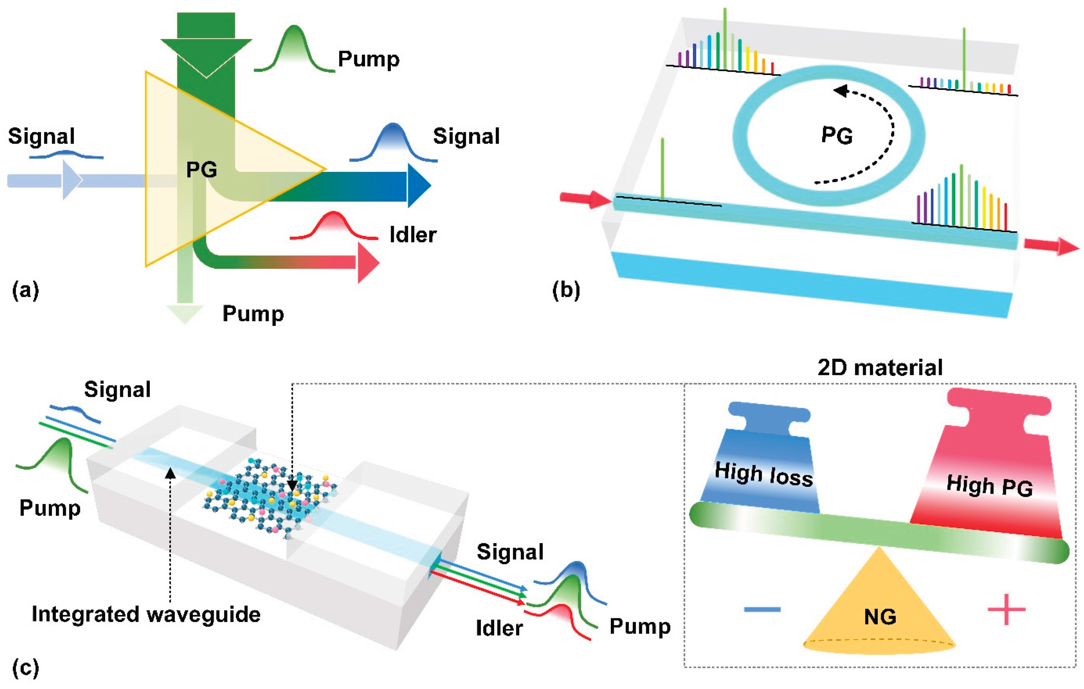
Figure 2.
(a) Schematic illustration of a SiN waveguide with a cross-section of 1600 nm × 720 nm, where (i), (ii), and (iii) show the three-dimensional (3D) view, cross-sectional view, and TE mode profile (at 1550 nm), respectively. (b) PG for the waveguide in (a) excited by using a continuous-wave (CW) pumping, where (i) shows the PG versus waveguide length (L) and propagation loss (PL) with a CW pump power (PCW) of 2 W, (ii) and (iii) show the PG versus L and PCW with PL = 0.5 dB/cm and 0.02 dB/cm, respectively. (c) PG for the waveguide in (a) excited by using a pulsed pumping, where (i) shows the PG versus L and PL with a pulse pump power (Ppulse) of 180 W, (ii) and (iii) show the PG versus L and Ppulse with PL = 0.5 dB/cm and 0.02 dB/cm, respectively. In (b) and (c), the black points and asterisks mark the results simulated using the parameters of practical devices in Refs. [1,22].
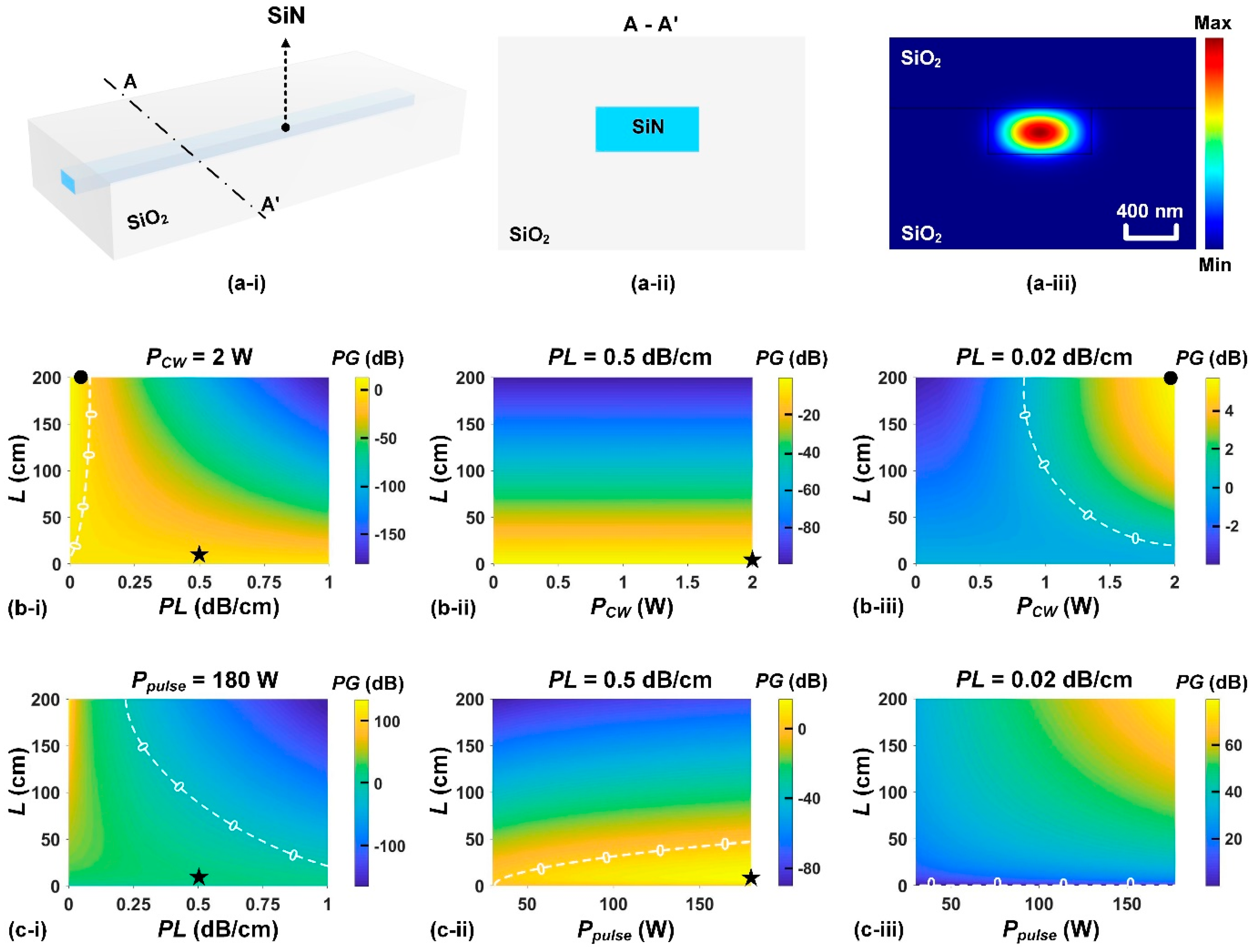
Figure 3.
(a) Schematic illustration of a silicon nanowire waveguide with a cross-section of 450 nm × 220 nm, where (i), (ii), and (iii) show the 3D view, cross-sectional view, and TE mode profile (at 1550 nm), respectively. (b) PG for the waveguide in (a) excited by using a CW pumping, where (i) shows the PG versus L and PL with PCW = 2 W, (ii) and (iii) show the PG versus L and PCW with PL = 4.3 dB/cm and 1.0 dB/cm, respectively. (c) PG for the waveguide in (a) excited by using a pulsed pumping, where (i) shows the PG versus L and PL with Ppulse = 180 W, (ii) and (iii) show the PG versus L and Ppulse with PL = 4.3 dB/cm and 1.0 dB/cm, respectively.
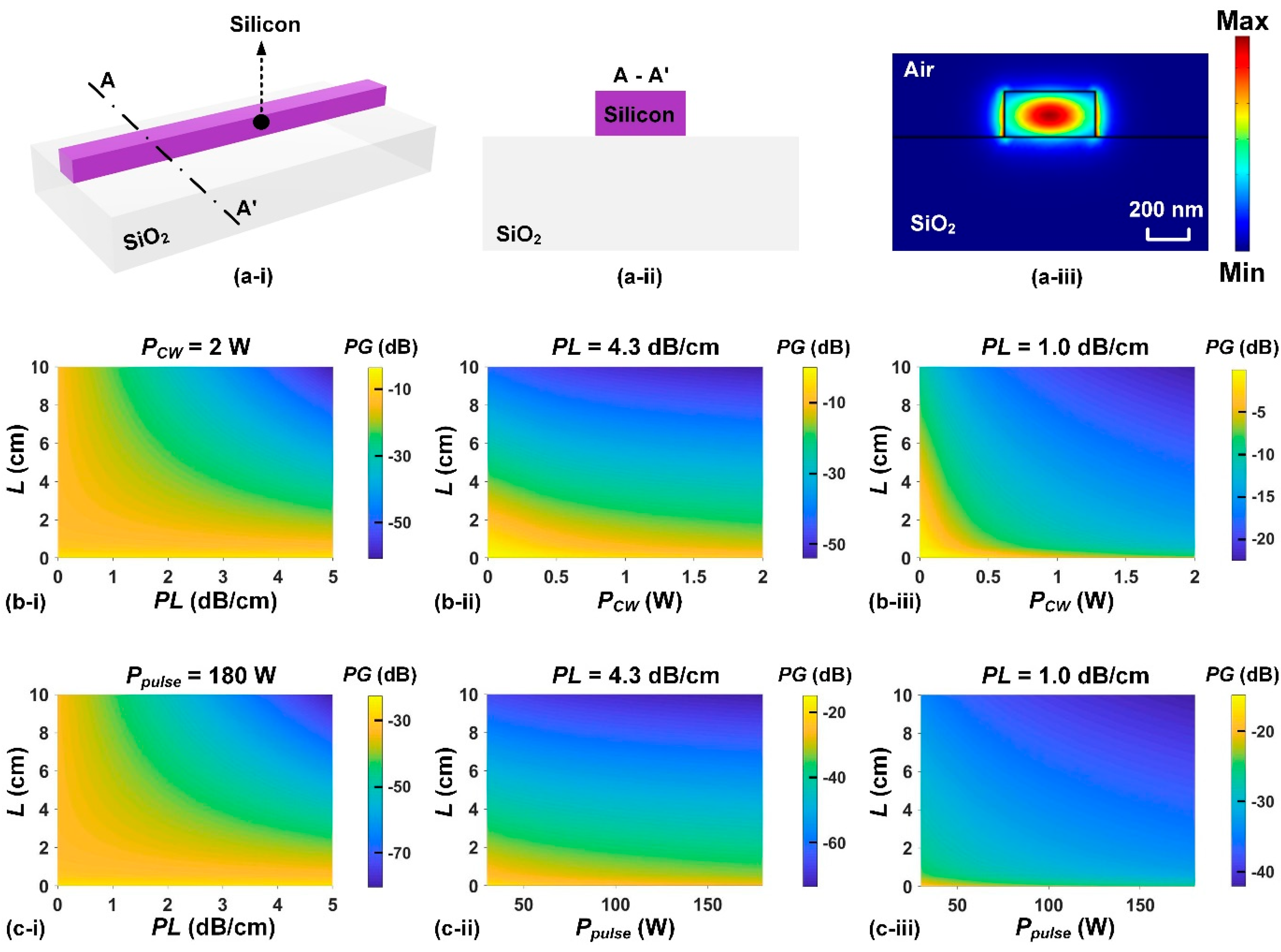
Figure 4.
PG analysis for (a) a silicon rib waveguide with a cross-section of 1000 nm × 380 nm and an etched depth of 70 nm for the cap, (b) a silicon etchless waveguide with a cross-section of 1000 nm × 70 nm, and (c) a silicon slab waveguide with a cross-section of 900 nm × 60 nm. In (a) ‒ (c), (i) shows the TE mode profile (at 1550 nm), (ii) shows the PG versus L and PCW, and (iii) shows the PG versus L and Ppulse. The PL values of the silicon rib, etchless, and slab waveguides in (a) ‒ (c) are 0.4, 0.3, and 0.6 dB/cm, respectively.
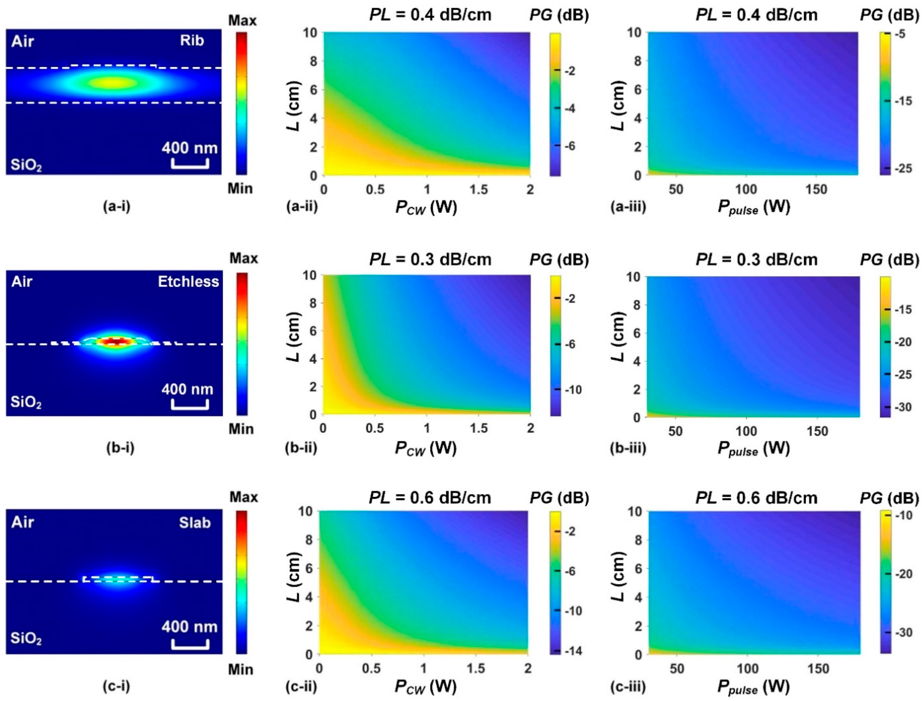
Figure 5.
PG analysis of silicon slot waveguides with (a) 100-nm, (b) 150-nm, and (c) 200-nm slot widths. In (a) ‒ (c), (i) shows the TE mode profile (at 1550 nm), (ii) shows PG versus L and PCW, and (iii) shows PG versus L and Ppulse. Each silicon waveguide on both sides of the slot region has a cross-section of 225 nm × 220 nm. The PL values of the waveguides in (a) ‒ (c) are 4.1, 5.0, and 6.3 dB/cm, respectively.
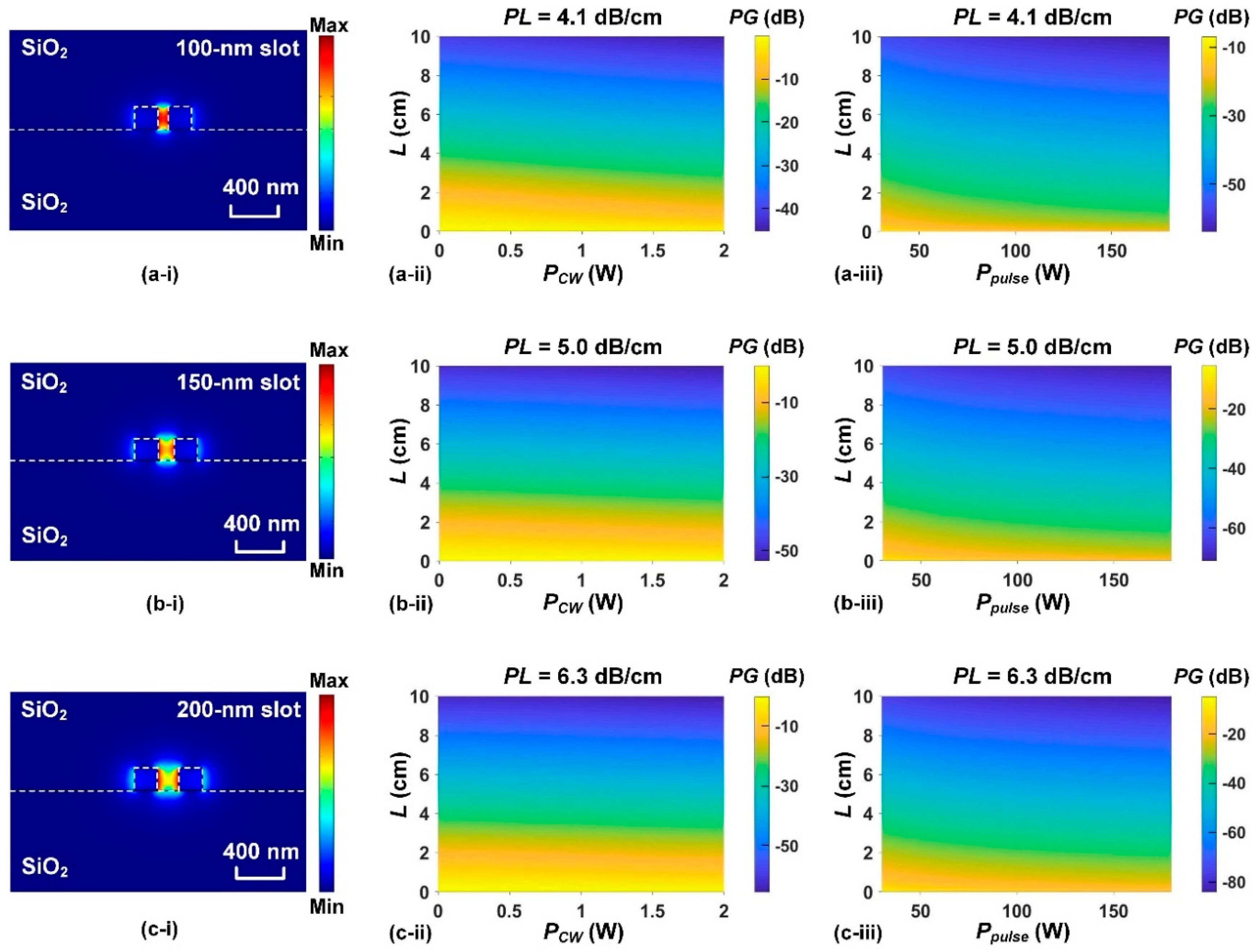
Figure 6.
(a) Schematic illustration of a SiN waveguide integrated with monolayer GO films, where (i), (ii), and (iii) show the 3D view, cross-sectional view, and TE mode profile (at 1550 nm), respectively. (b) PG for the hybrid waveguide in (a) excited by using a CW pumping, where (i) shows the PG versus L and PCW when the excess propagation loss induced by GO (EPLGO) is 3.0 dB/cm, (ii) shows the PG versus L and EPLGO with PCW = 0.2 W, and (iii) shows the PG versus EPLGO and PCW with L = 2 cm. (c) PG for the hybrid waveguide in (a) excited by using a pulsed pumping, where (i) shows the PG versus L and Ppulse with EPLGO = 3.0 dB/cm, (ii) shows the PG versus L and EPLGO with Ppulse = 180 W, and (iii) shows the PG versus EPLGO and Ppulse with L = 2 cm. In (b) and (c), the PL of the uncoated SiN waveguide is 0.2 dB/cm and the asterisks mark the results simulated using the parameters of practical devices in Ref. [1].
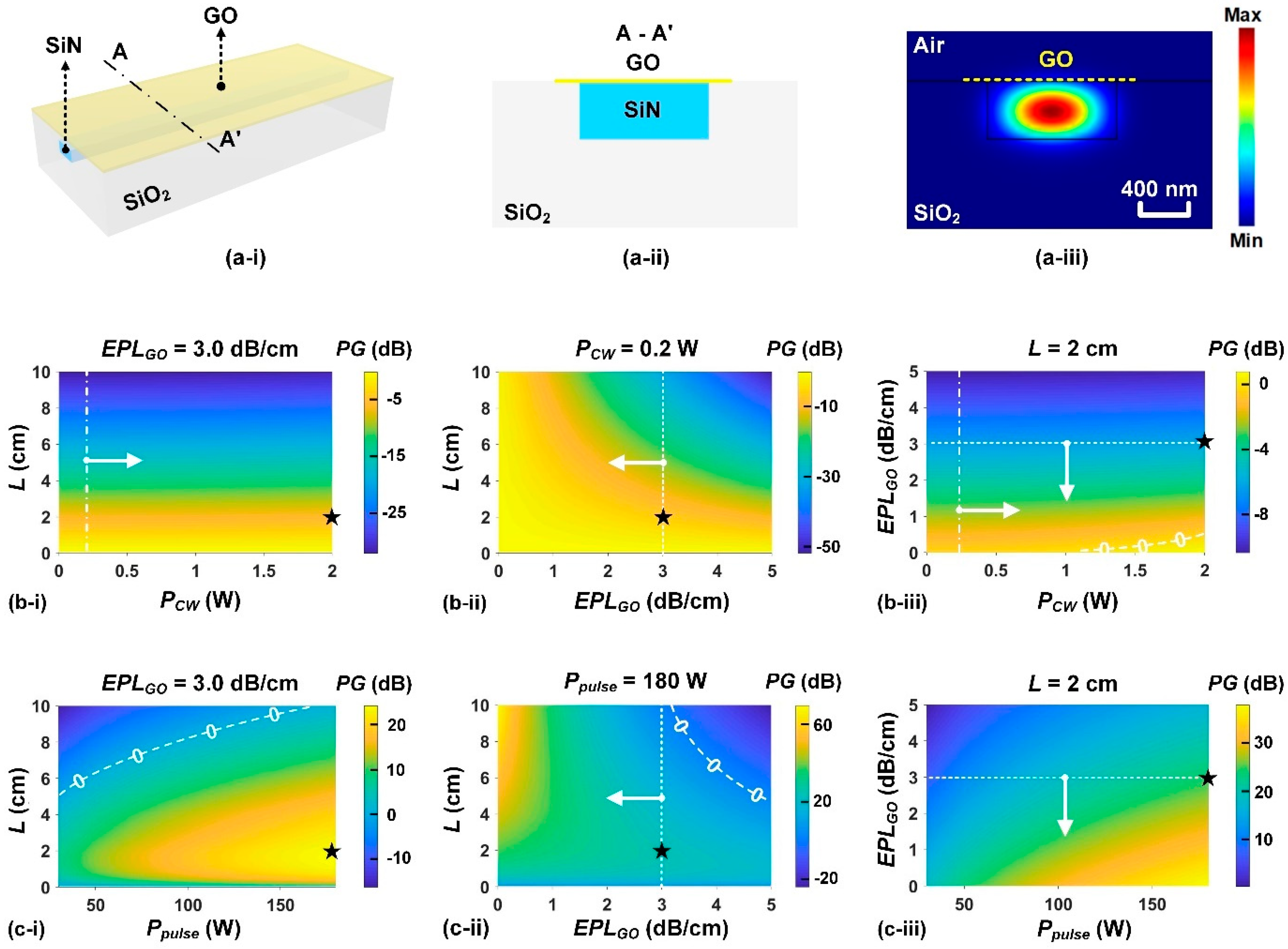
Figure 7.
(a) Schematic illustration of a silicon nanowire waveguide incorporated with monolayer GO films, where (i), (ii), and (iii) show the 3D view, cross-sectional view, and TE mode profile (at 1550 nm), respectively. (b) PG for the hybrid waveguide in (a) excited by using a CW pumping, where (i) shows the PG versus L and PCW with EPLGO = 20.5 dB/cm, (ii) shows the PG versus L and EPLGO with PCW = 0.1 W, and (iii) shows the PG versus EPLGO and PCW with L = 3 mm. (c) PG for the hybrid waveguide in (a) excited by using a pulsed pumping, where (i) shows the PG versus L and Ppulse with EPLGO = 20.5 dB/cm, (ii) shows the PG versus L and EPLGO with Ppulse = 20 W, and (iii) shows the PG versus EPLGO and Ppulse with L = 3 mm. In (b) and (c), the PL of the uncoated silicon waveguide is 1.0 dB/cm.
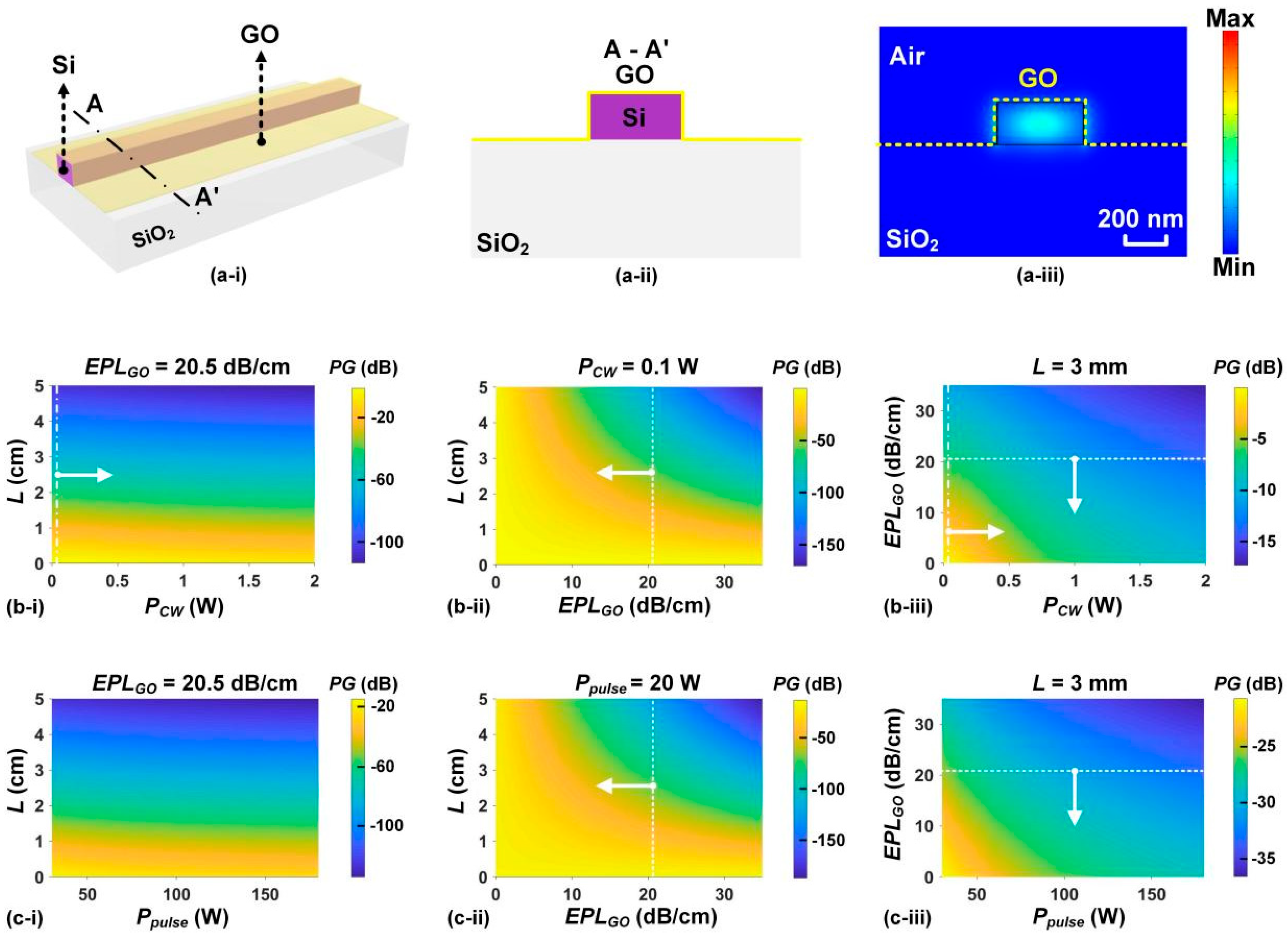
Figure 8.
PG analysis of three types of silicon waveguides integrated with monolayer GO films: (a) a rib waveguide (b) an etchless waveguide, and (c) a slab waveguide. In (a) ‒ (c), (i) shows the TE mode profile (at 1550 nm), (ii) shows the PG versus EPLGO and PCW with L = 1 mm, and (iii) shows the PG versus EPLGO and Ppulse with L = 1 mm. The PL values of the uncoated silicon rib, etchless, and slab waveguides are 0.4, 0.3, and 0.6 dB/cm, respectively.
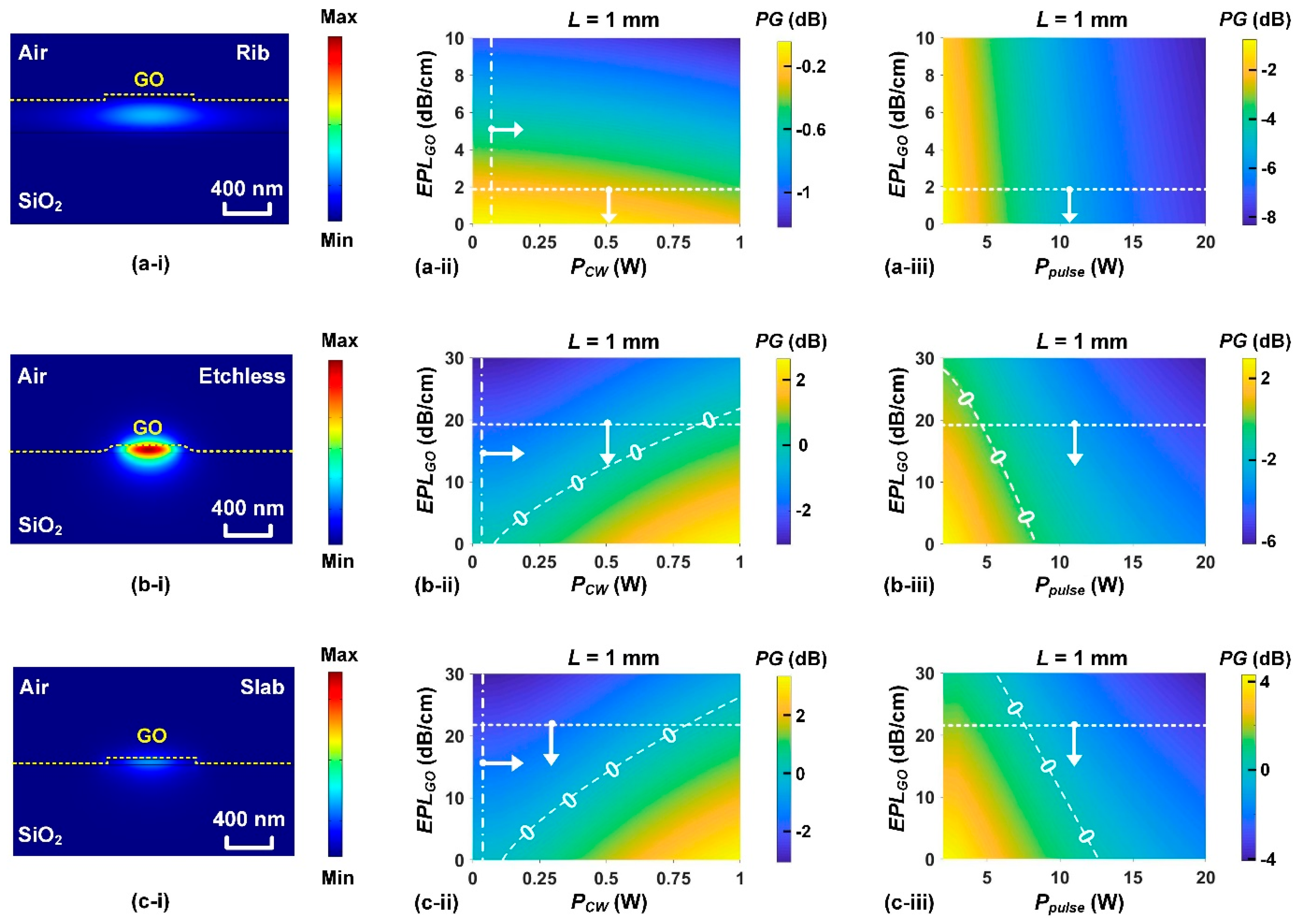
Figure 9.
PG analysis of GO-silicon slot hybrid waveguides with (a) 100-nm, (b) 150-nm, and (c) 200-nm slot widths. In (a) ‒ (c), (i) shows the TE mode profile (at 1550 nm), (ii) shows PG versus EPLGO and PCW with L = 1 mm, and (iii) shows PG versus EPLGO and Ppulse with L = 1 mm. The PL values of the uncoated waveguides are 4.1, 5.0, and 6.3 dB/cm, respectively.
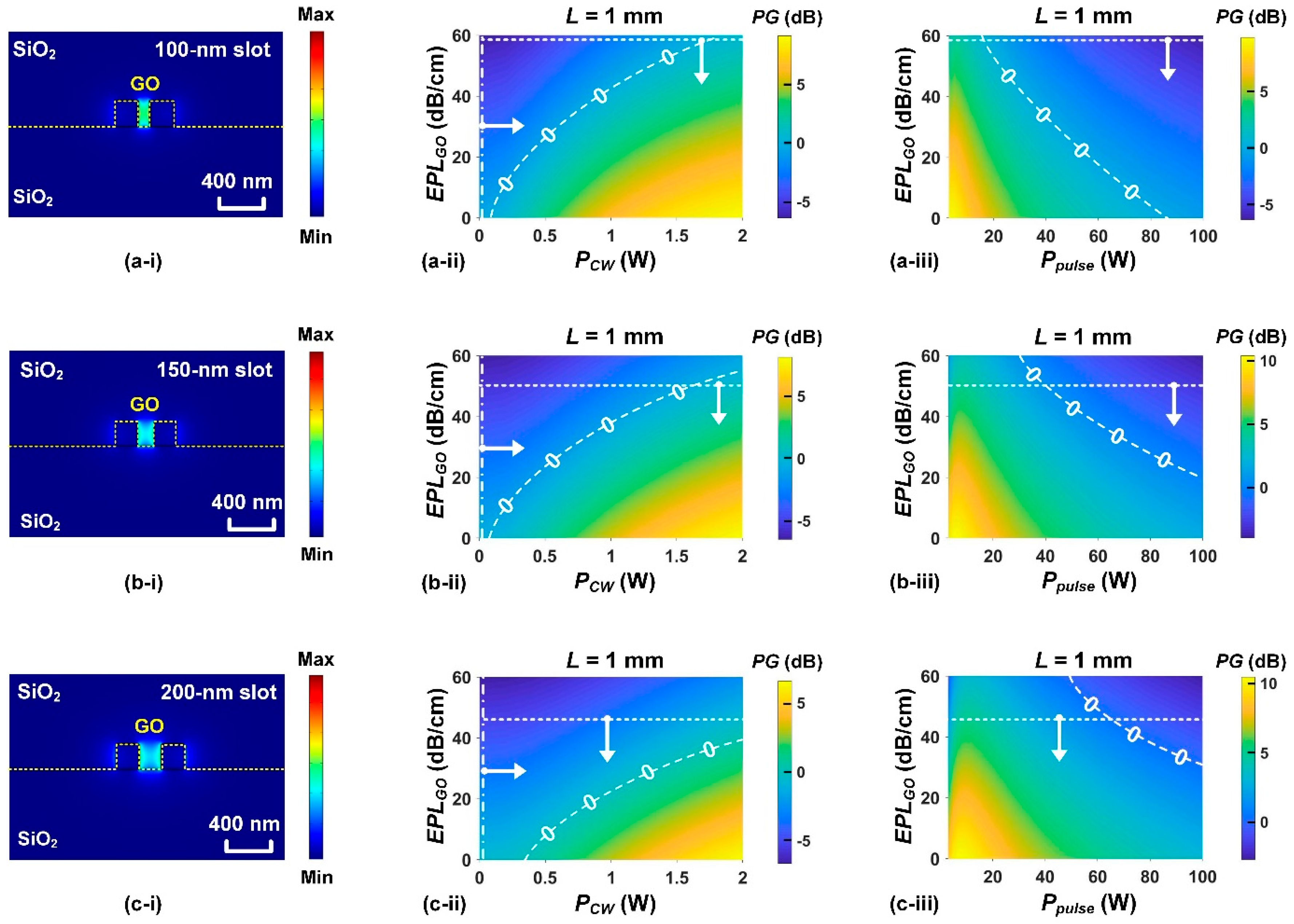
Figure 10.
Comparison of PG for (a) SiN waveguides and (b) silicon nanowire waveguides incorporating 2D GO, graphene, and MoS2 films, where (i) and (ii) show the PG versus PCW and Ppulse with L = 1 mm, respectively. In (a) and (b), the PL values of the uncoated SiN and silicon waveguide are 0.2 dB/cm and 1.0 dB/cm, respectively.
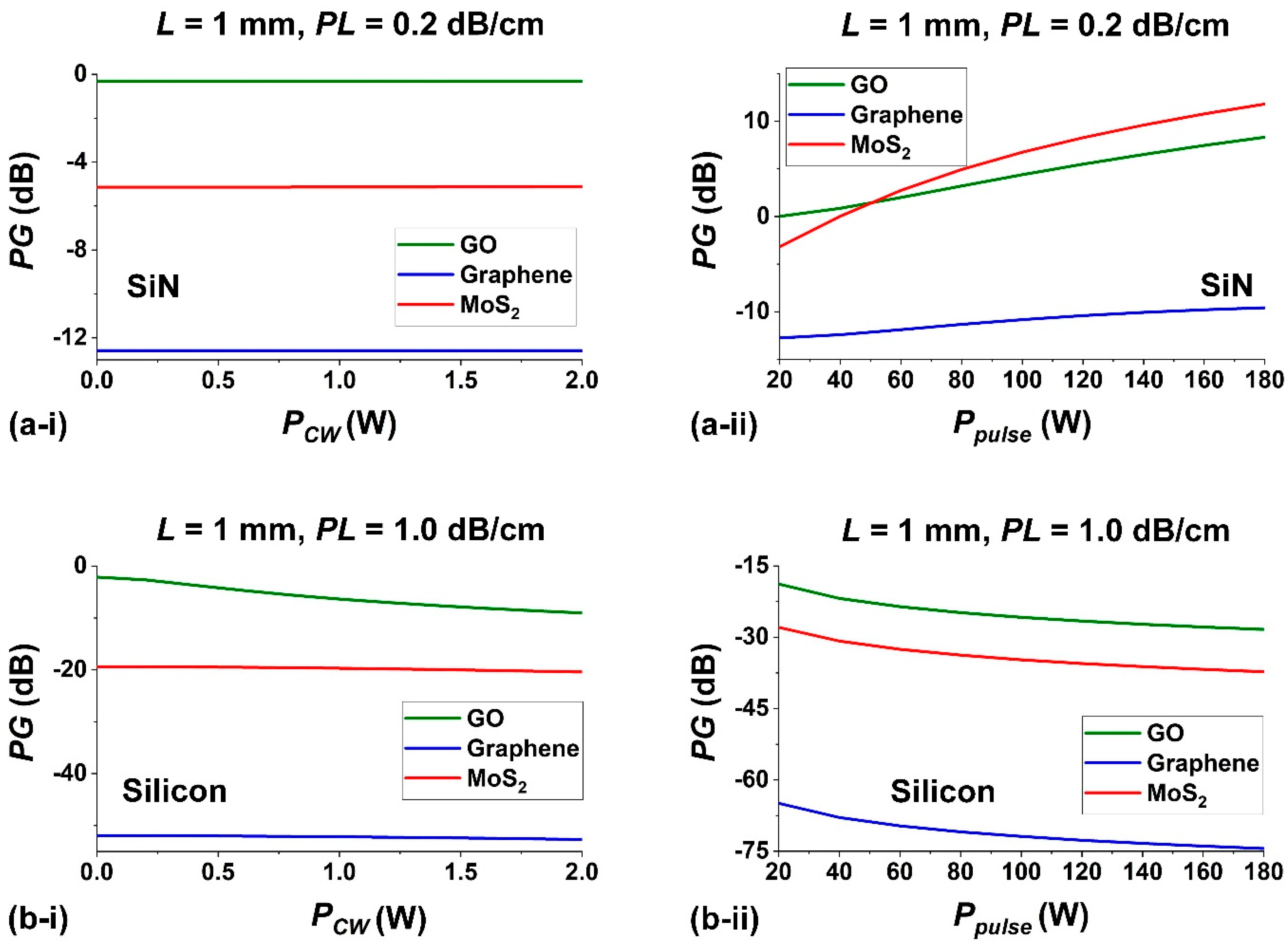
Disclaimer/Publisher’s Note: The statements, opinions and data contained in all publications are solely those of the individual author(s) and contributor(s) and not of MDPI and/or the editor(s). MDPI and/or the editor(s) disclaim responsibility for any injury to people or property resulting from any ideas, methods, instructions or products referred to in the content. |
© 2026 by the author. Licensee MDPI, Basel, Switzerland. This article is an open access article distributed under the terms and conditions of the Creative Commons Attribution (CC BY) license.
Copyright: This open access article is published under a Creative Commons CC BY 4.0 license, which permit the free download, distribution, and reuse, provided that the author and preprint are cited in any reuse.


