Submitted:
04 February 2026
Posted:
05 February 2026
You are already at the latest version
Abstract
This article discusses the additive manufacturing and post-processing of axicons, and their performance evaluation using attenuation and near-field-measurements based fundamental techniques. The axicons are manufactured using the materials cyclic olefin copolymer (TOPAS) and polymethyl methacrylate (PMMA), for their respective use in terahertz and near-infrared applications. An emphasis is placed on the dip-coating-based post-processing. Interval dipping and intermittent hardening lead to excellent surface finish and transparency in case of additively-manufactured near-infrared axicons. The dip-coated samples exhibit surface roughness of sub 10 nm, and a uniformly distributed thin layer coating over the axicon surface. In addition to the improved surface finish and transparency, the coatings are also closely matched in refractive index to the axicon material. Such post-processed axicons pave the way for rapid-prototyping and production.
Keywords:
additive manufacturing
; stereolithography
; dip-coating
; post-processing
1. Introduction
Additive manufacturing (AM) of optical components is widely used for rapid prototyping and swift error correction [1,2]. Techniques such as stereolithography apparatus (SLA) and material jetting based 3D-printing processes, e.g., inkjet 3D-printing using transparent materials enable the fabrication of optical components such as lenses, plastic optical fibers (POFs), and waveguides [3,4,5,6]. Implementation of photopolymerization based manufacturing helps to develop complex geometrical structures, e.g., Fresnel lenses, Fresnel axicons, and diffraction gratings [7,8]. Additionally, AM facilitates the production of other optical components such as optical multi-material meta-surfaces and phase modulation elements [2,9]. Therefore, it is evident that when AM is combined with the optical component prototyping, a cost-efficient alternative for current manufacturing techniques can be derived [10]. However, the objects manufactured using polymer based AM possess high surface roughness of the order of few µm [11]. For employing these prototypes in applications of optics, a post-processing based approach is necessary. Simple hand polishing and lacquering based approaches bring surface roughness down to 5 , which is not sufficient for optical applications [12]. Additionally, state-of-the-art coating techniques based on high temperature processing are expensive and tedious [13,14]. Other dip-coating based approaches also exist and are typically derived from spraying lacquer over the surface to be coated, or by a completely automated complex industrial dip-coating procedure developed only for coating filament-based prototypes [15,16,17]. Such coating-based techniques can achieve nano-meter scale surface roughness [18], using various dip-coating techniques defined for optical waveguides and fibers [19]. However, very few techniques propose a simplified and cost-efficient approach for coating of lenses, e.g., our previous research [20].
Building upon current state-of-the-art designs of additively-manufactured axicons, reference [21] proposes a micro-axicon based design for endoscopes. Notably, most of the applications of axicons appear in tomography and endoscopy, enabling improved imaging with large depth of focus (DOF) [22]. Similarly, reference [23] reports on 3D-printed axicons and phase plates composed of polypropylene (PP) and high density polyethylene (HDPE) for terahertz (THz) applications. Reference [24] summarizes detailed designs, parameter estimations, specific types of axicons, and their applications. Moreover, as discussed in reference [25], 3D-printed axicons of different apex angle for THz spectral range are evaluated for generation of arbitrary order Bessel beams. Motivated by these developments, we propose axicons for near-infrared (NIR) and THz applications. Such axicons can aid in the in- and outcoupling of THz waves [26] in waveguide-based biosensors, and hold promise for their equivalent NIR counterparts.
This article extends our previous work from reference [26], where we investigated the AM and performance of THz axicons, with and without a dip-coating-based post-processing technique. Here, we concentrate on AM of axicons for implementation in NIR spectroscopy and present the fundamental results and analysis of the additively manufactured and post-processed NIR axicons at 1550 . The outline of this article is as follows. Section 2 introduces axicons, briefly followed by the corresponding design parameters. Section 3 gives an overview of the manufacturing strategies and post-processing techniques. Section 4 discusses the results for additively manufactured THz axicons presented in reference [26], followed by the results obtained for the NIR axicons. Section 5 summarizes the experimental evaluation, followed by the conclusion and outlook.
2. Theory and Design
Axicons are a special type of lens characterized by a different geometry compared to conventional spherical lenses. An axicon has a conical front surface and relies on diffraction to obtain a long focal depth [27]. The shape of an axicon resembles a tip and differs fundamentally from the curved surfaces of classic converging lenses. The special geometry of an axicon guides the light as it passes through the same. Unlike convex lenses that focus a parallel light beam around the focal point of the lens, the axicon produces an elongated focal depth profile called an interference line or DOF. This offers an advantage in applications where an elongated focal line is desired for imaging or spectroscopy. The applications of axicons include astronomy where parallel ring beams are generated. They are also implemented especially in the medical field for eye surgery and endoscopic imaging [24]. Moreover, the very basic use of axicons is in wave optics where Bessel beam generation is necessary. Axicons are usually manufactured using injection molding and preform-based heated molds, followed by polishing and milling. A separate milling of glass also produces axicons. Another interesting method for manufacturing axicons is diamond turning, and is used for high-precision axicon manufacturing without requiring any post-processing [28]. However, these processes are non-trivial and lack the rapid prototyping and error correction step. Therefore, the authors concentrate on manufacturing the axicons using additive-manufacturing-based processes, e.g., SLA [29].
For the defined range of the DOF of an axicon, a special light distribution is produced by the incident parallel light rays. The incident gaussian beam guides itself into a second-order Bessel beam and forms concentric rings. This beam has different properties compared to its gaussian counterpart. Gaussian beams generally diverge in the direction of propagation of light, thereby decreasing the intensity of the beam. However, Bessel beams show almost constant intensity distribution transverse to the direction of propagation. The beam properties within the range of DOF are nearly uniform, similar to a non-diffracting beam. It is however only theoretically possible to generate perfect Bessel beams, and axicons can only produce nearly perfect Bessel beams [30].
Figure 1.
Pictorial representation of an axicon depicting the formation of Bessel beams after the DOF region [29].
Figure 1.
Pictorial representation of an axicon depicting the formation of Bessel beams after the DOF region [29].
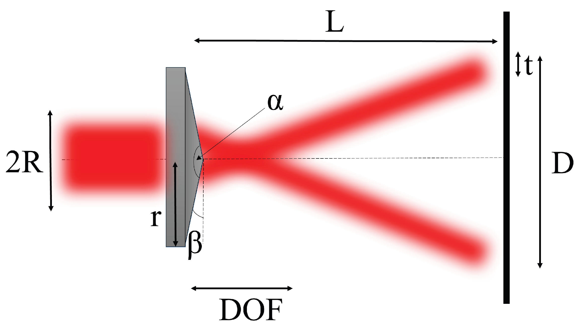
To design axicons, we used the traditional approach based on apex angle calculations. The length of the DOF region is approximated using equation 1, where R is the radius of the incident light beam, n is the refractive index of the axicon material, and is the cone angle [31]. Cone angle is calculated using the predefined apex angle () of the axicon. The simplified formula given in equation 1 approximates quite accurate results for smaller cone angles, but it is recommended to use the extended version for larger cone angle based calculations.
The second-order Bessel beam forms an interference ring behind the DOF region. The thickness of this ring (t) corresponds approximately to the radius of the incident light beam.
The analytical calculations using equation 2 give the thickness of the interference ring. Furthermore, we also calculated ring diameter of the interference ring () using the simplified equation 3.
There is a linear relationship between the ring diameter and the distance between the formed ring and the axicon. Another important parameter in the designing of axicons is the height of the axicon. We used equation 4 to calculate the height of the axicon (h), where r is the radius of the axicon and is the cone angle.
For the calculation of the DOF, the authors used the alternate angle of apex angle (cone angle or ). In case of NIR beams, as the collimated light beam emitted by the laser source is a gaussian beam, the method is initially utilized to approximate the radius of the light beam. This method is based on a fixed intensity threshold, and is used in international standards, e.g., in laser safety assessment. This method defines the beam radius where the intensity has dropped to where is the initial intensity [32]. Based on a few reference measurements and method calculations in MATLAB, we approximate the NIR beam diameter as 10 . For the THz beam, the approximated beam diameter due to the placement of an aluminum foil-based circular aperture before the axicon, does not exceed 20 mm for the investigated frequencies. Subsequently, further design parameters for axicons of apex angles 140° 150° and 160° were calculated using MATLAB to design the axicons of three different apex angles.
For the TOPAS material used to manufacture THz components [12], the measured refractive index between and is approximately 1.53, and for clear resin material (for NIR components), the refractive index at 1550 nm is 1.49. Table 1 shows the design parameters of NIR and THz axicon with apex angles of 140°, 150° and 160°. With the help of these design parameters, we then designed the axicons in Autodesk Fusion 360. Initially, a triangle based sketch is designed with the height of the axicon mentioned in Table 1, and desired radius of the axicon, followed by the use of the rotate function to create the conical axicon surface. The authors provided a thickness of 10 mm to each axicon in case post-processing requires better grip. These axicons also possess three stripes at 120° each to be fitted inside their holders before further post-processing (explained in detail in Section 3). Figure 2 shows the exemplary 3D-representation and 2D-sketch of the axicon of apex angle 140°, with thickness designed in the software Autodesk Fusion 360.
3. Methodology
AM of optical components is a four-step process in which the 3D-CAD, standard triangulation language, or standard tessellation language (STL) file is initially sliced. This is followed by the prototype manufacturing with the help of layer-by-layer deposition. The component then undergoes post-processing to achieve the required transparency and attenuation. Our previous research from references [12] and [13] thoroughly discuss the currently available materials and suitable processes for AM of NIR and THz components. The fabrication of THz-based waveguides and axicons usually utilizes TOPAS as the filament material as it shows low absorption of the THz beam [12]. In the 3D-printer used for manufacturing of THz axicons from our previous research [26] (Bambu Lab X1E), filament deposition onto the build platform was carried out using the fused filament fabrication (FFF) process. The axicons were fabricated using an aligned rectilinear infill pattern and a layer-by-layer manufacturing process. A material flow ratio exceeding 100% compensated for air gaps formed during the filament deposition.
As an extension to the work described in reference [20], this study utilizes a PMMA-based resin and SLA process for the manufacturing of NIR axicons. The newly fabricated NIR axicon shares the same design parameters as the THz axicon in reference [29], featuring a apex angle. A Formlabs Form 3 SLA-based 3D-printer and Formlabs Clear resin V4 were used to manufacture the axicons. The fabrication process orients the axicons such that the flat surface contains the support structures, which surround the surface to prevent the formation of in-process satellite drops, and are removed later by mechanical breaking. The 3D-printer uses low force SLA, which facilitates support removal without affecting the surface finish. After printing, the structures were washed in isopropyl alcohol to remove any residual resin, and were subsequently hardened under UV-light. The bottom flat surface was polished using a wet-grinding machine, while the top surface remained unpolished to avoid structural deformation and potential parameter alterations. An improved and enhanced dip-coating process acts as the final post-processing step. This improved technique (termed hereafter as enhanced dip-coating) differs from the previous method (termed hereafter as simple dip-coating) reported in our research from reference [20], which contained the following steps:
- 1.
- Heating the PMMA-based resin to C, followed by immersing the optical components in heated resin for approximately 10 .
- 2.
- A UV-hardening unit (Formlabs Form Cure) operating at a wavelength of 405 and with heating at C hardened the coated samples continuously for up to 30 .
An initial Snell’s law based verification of the refractive index of the half cylindrical samples evaluated the effects of hardening and dip-coating on the refractive index of the resin [7]. Refractive index of the resin after washing remains the same as that of the liquid resin. After hardening, the refractive index of the material increases to 1.53. Additionally, a yellow hue and a few satellite drops were occasionally present in the post-processed samples. The enhanced approach presented in this manuscript resolves these drawbacks by performing multiple dip-coating cycles (interval dipping) lasting more than 10 , separated by 20 – 30 intervals, to achieve a uniform coating layer.
An intermittent hardening technique then cures the samples to suppress coloration and satellite droplet formation. Hardening was performed at C in 5 intervals, and was repeated up to five times. Figure 3 shows a step-by step enhanced dip-coating approach based on interval dipping and intermittent hardening. Furthermore, the authors also computed the relation between dipping and hardening time based on surface tension, thermal diffusivity and thickness of the object to be coated, and dipping thickness [33]. Based on the relaxation time () equation from the Landau-Levich-Derjaguin Problem [34] of viscous liquid, with as viscosity and L as flow scale is given in equation 5.
The derived dipping time and hardening time are given in equations 6 and 7.
Here, l is the thickness of the lens, is the thickness of the coating layer, and is the thermal diffusivity.
Figure 4 depicts the achieved transparency after the enhanced dip coating process for THz and NIR axicon samples. The samples coated using the enhanced dip-coating are later mounted on holders 3D-printed using PLA in an FFF-based Prusa MK3S+ 3D-printer. These holders are specially designed to fit inside the curing device (in this particular case, Formlabs Form Cure) so that the bottom surface of the 3D-structures does not touch the curing surface of the Form cure. The holders also avoid imprinting the dust or resin residue particles on the dip-coated surface. These holders provide sufficient grip for the intermittent hardening process.
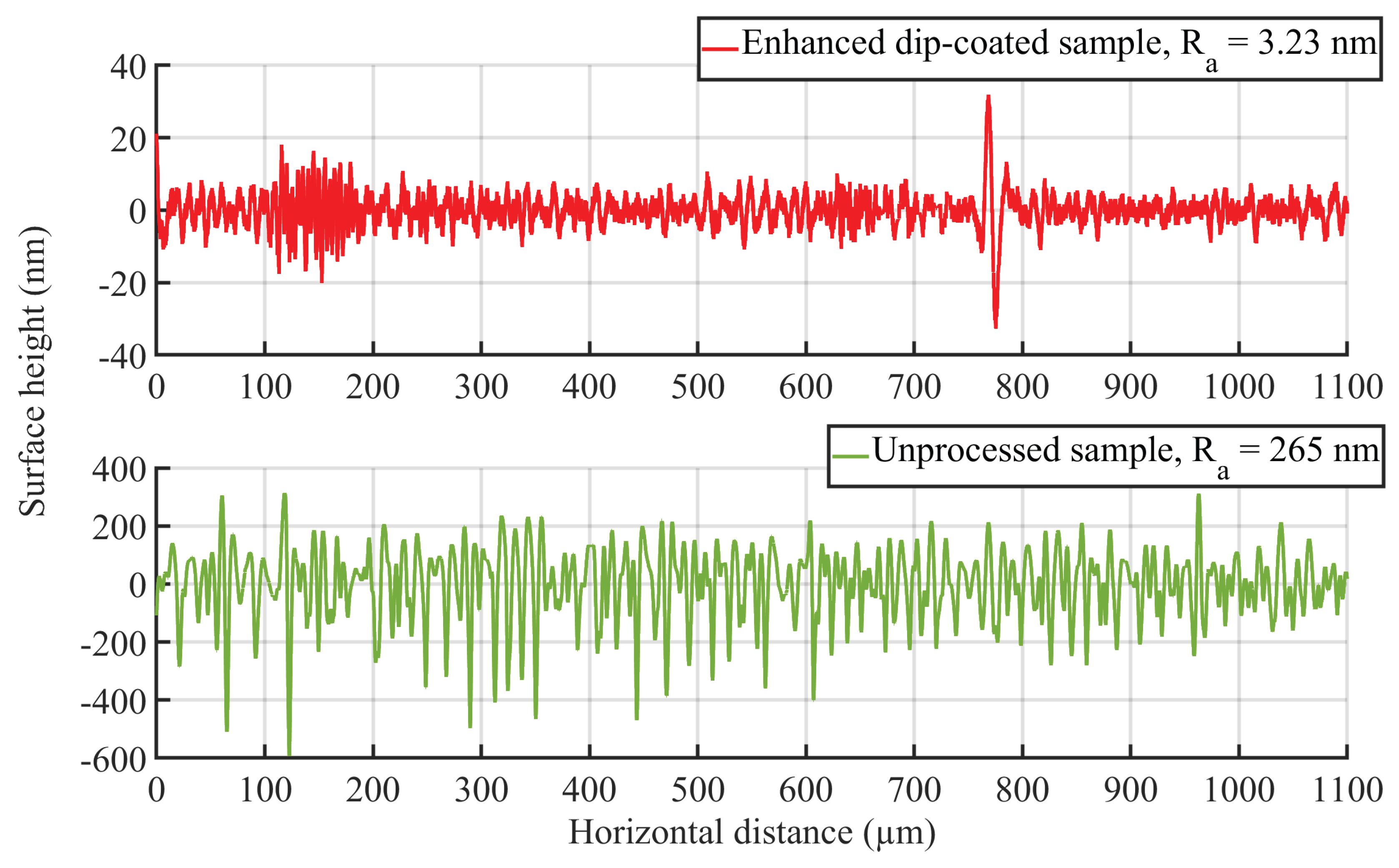
The authors concentrated only on post-processing using the Formlabs clear resin material to avoid refractive-index mismatch and probable Fabry Pérot effects. Research is currently being carried out with other suitable materials, e.g., Acrylonitrile Butadiene Styrene, Ormocore, and SU-8 as they show nearly similar refractive indices as the Formlabs Clear resin. Comparing with prior studies from reference [20], the enhanced dip-coating process differs in dipping the prototype in the solvent and continuous hardening. The enhanced approach shows that the combination of interval dipping and intermittent hardening offers an improved finish of the axicon surface. Moreover, the refractive index of the hardened layer and the axicon material stabilizes at 1.53 following the enhanced dip-coating process. A profilometer (DEKTAK 6M from Bruker Corporation) measured the surface roughness of the samples. The surface roughness (arithmetic average of surface deviation) of the enhanced dip-coated sample is sub 10 and the thickness of the uniform coating layer measured after hardening is 10 . Corresponding measurement results are plotted in Appendix A. Additionally, a Mitutoyo profilometer and Keyence VHX7000 microscope were also used to assess the surface roughness; however, due to their resolution-limited measurement accuracy, these results are excluded from further analysis. A total of eight samples were manufactured and characterized. Two samples were left unprocessed, while two samples each were post-processed by simple dip-coating, enhanced dip-coating, and polishing at the bottom surface. All samples were fabricated using identical design parameters to ensure reproducibility and to validate the obtained results.
4. Results and Discussion
The authors initially carried out the characterization of THz axicons. Reference [26] details the experimental setup for this measurement. The distances chosen (55 mm and 82 mm) correspond to regions in the vicinity or within the DOF of the axicon for the frequencies in the range of 100 - 200 . Figure 5 illustrates the normalized intensity distribution of unprocessed and dip-coated THz axicons manufactured using TOPAS and the FFF process. There was a negligible difference in the beam profiles of the two axicons as the film thickness remains a small fraction of the THz wavelength (here 1 - 3 ). For NIR, however, the situation differs: if the coating material (Formlabs Clear Resin V4) differs from the base material (TOPAS) of the axicon, a minor refractive index mismatch can occur, which leads to potential Fabry-Pérot effects. Such issues can be mitigated by using identical materials or a material with very slight index mismatch. The enhanced dip-coating process and the same dipping solvent described in Section 3 were employed for post-processing of the NIR axicons. The surface roughness achieved using the simple dip-coating process and the enhanced dip-coating process is tabulated in Table 2.
Figure 6 illustrates the experimental setup for the NIR axicon evaluation. The setup includes a Thorlabs MCLS1 fiber–coupled laser module that provides four selectable wavelengths ( 635 , 850 , 1310 , and 1550 ). For the analysis of NIR axicons, the 1550 output was selected, delivering of optical power. The laser beam exits the multimode FC/PC fiber patch cable (with 50 core diameter) into free space, where a conventional convex lens (C-L) is used to align the setup and form a quasi-parallel transmission beam. The Anritsu ML9001A power meter with 1550 detector module is placed on an automated XYZ stage, operated by a Newport MM4006 motion controller.
The detector and power-meter readings determine the approximate beam diameter at the incident plane of the additively manufactured axicon lens (AX-L). The AX-L features a diameter of 30 , ensuring that the optical beam remains non-truncated. A reference measurement without the axicon provides a baseline for subsequent analysis. The beam profile of a 1550 beam transmitted through an axicon with apex angle of was first calculated and later compared with measured and processed experimental results (see Figure 7, dashed plot). Initially, the distance set between the detector module and the calculated DOF is 5 . Unprocessed and post-processed (polished at the bottom surface, dip-coated and enhanced dip-coated) axicons are then placed between the convex lens and the detector one after another to analyze the DOF of the axicon. The detector scans the axicon’s calculated DOF region in 2 steps. The results demonstrate that the dip-coated axicon focuses the beam within the DOF region, whereas the unprocessed axicon fails to achieve this. As the detector uses an aperture with a diameter of , the data is integrated and normalized to the detector area and then an image-processing based evaluation is used to correctly represent the measured results.
The authors used the following image processing tools (described here step-by-step) to generate the final comparison of the DOF results.
- 1.
- Digitization: The continuous image is scanned at fixed raster positions. The underlying grid is determined by the sensor architecture [35].
- 2.
- Interpolation: Interpolation is used to obtain the continuous signal from the digitized and discrete scan. It is based on the probability of finding how the particular points contribute in creating a new point. A MATLAB interpolation tool is used to approximate the interpolation kernels, as the perfect interpolation is complex to achieve. This implementation includes both linear and spline interpolation. Linear interpolation is a classic approach and uses interpolated points lying on a straight line to connect to a neighboring grid. It is a simple but inaccurate approach, and leads to smoothing of image and spectral errors where the wave number is higher. However, the spline interpolation method uses polynomials connected at the nodes under continuity conditions. This method produces smooth curves unlike linear interpolation. Cubic spline is also one of the types of spline interpolation that provides smoothing of the image.
- 3.
- Deconvolution: At the end of image processing, deconvolution using a point spread function is utilized. This is the final image reconstruction step using inverse filtering and Wiener deconvolution. A mathematical representation explaining a measured image b, point spread function c, and original image X is given by equation 8, where is the additive noise independent of the signal.The measured image acts as a low pass filter attenuating high frequency image details. It is observed that the Wiener deconvolution is a robust method of decompressing that delivers consistent results using the measurement data.
Finally, the raw and processed data sets are compared to verify the DOF of the NIR axicons. Figure 7 shows an exemplary result depicting the data-processed plots for the beam profile of the axicons (unprocessed, polished at bottom surface, simple dip-coated and enhanced dip-coated) with an apex angle of . It can be concluded from these results that the beam profile of the enhanced dip-coated axicon and simple dip-coated axicon matches with the analytical results derived from our design parameters.
Figure 8 shows the total integrated power for the enhanced dip-coated axicons and simple dip-coated axicons for varying detector positions. The output power measurements indicate that the strongest power concentration occurs within the half of the DOF region, located between 13 and 17 . For both the samples, the authors observed the maximum integrated total power of approximately and in this particular region. This region aligns well with the original design parameters and is considered as the beginning of the DOF region. The total integrated power starts dropping after the distance of 33 , followed by the formation of an interference ring, which results in the convolution of second order Bessel beams at 60 for the considered axicon. The enhanced dip-coated axicon shows less attenuation of the beam as compared to simple dip-coated samples due to uniform coating and reduced satellite drops. Enhanced dip-coating also makes sure that the scattering due to satellite drops and yellow hue is avoided. It is also observed that the high absorption in the unprocessed axicons prevents any clear or reliable conclusions regarding the DOF and the beam profile. From these results, it is evident that the enhanced dip-coating process with interval dipping and intermittent hardening, provides higher transparency, better finishing in terms of surface roughness, reduced attenuation, and marginal effects on the targeted refraction. The reduced surface roughness also promises better wave propagation with minimal scattering. Finally, two NIR axicon samples of apex angles 150° and 160° were additively manufactured and post-processed using the enhanced dip-coating process. Similar experiments to measure the beam profiles of both axicons are carried out using the experimental setup shown in Figure 6.
A comparatively similar behavior is observed for the same, reinforcing the critical role of dip-coating based post-processing. The comparison of the beam profiles for measured enhanced dip-coated axicon samples with analytical calculations for axicons of apex angles 150° and 160° is shown in Figure 9.
5. Conclusions and Outlook
In this work, we manufactured and characterized THz and NIR axicons with three different apex angles. THz axicons were produced using the FFF process with a TOPAS filament, and NIR axicons were manufactured using the SLA process with a PMMA-based Formlabs Clear resin V4. Without post-processing and by using the previously studied post-processing techniques, minimal measurable changes occur in the beam pattern within the DOF region for THz-axicons. To further improve the surface finish, we enhanced the simple dip-coating method from our previous research with the aid of interval dipping and intermittent hardening. The enhanced process increased the transparency of the axicons and avoided the formation of satellite drops and a possible yellow hue during the dip-coating process. The new coating reduced the surface roughness to sub 10 nm, and ensured a uniformly distributed thin coating layer. These improvements also occur for NIR axicons. Using such a closely-index-matched resin for the coating also minimizes any Fabry-Pérot related effects in both THz and NIR axicons. The resulting DOF parameters and beam profile for the dip-coating based post-processed axicons match with the intended design parameters. The repetitive measurements using two different samples of each NIR axicon with apex angle of 140°, 150° and 160° also prove the reproducibility of results using AM and successive dip-coating-based post-processing. The authors are currently extending the scope of employed materials and are working on bringing thin-film coatings using the enhanced dip-coating process for other additively-manufactured NIR components. An investigation into ultra-precise dispensing and vapor deposition is also being carried out for further reduction of surface roughness.
Author Contributions
Conceptualization, A.S., A.St., S.J.; methodology, A.S.; validation, A.S.; measurements and formal analysis, A.S., A.St., S.J.; investigation, A.S.; resources, A.S., S.J., A.St.; writing—original draft preparation, A.S.; writing—review and editing, A.S., A. St., S.J., S.P., O.S.; supervision, S.P., O.S.; project administration, A.S., S.P., O.S.; funding acquisition, S.P., O.S. All authors have read and agreed to the published version of the manuscript.
Funding
This research was funded by Deutsche Forschungsgemeinschaft (German Research Foundation) grant number 502254396 and the APC were funded by the Open Access Funds of Technische Hochschule Ostwestfalen-Lippe and Technische Universität Darmstadt.
Data Availability Statement
Data underlying the results presented in this paper are not publicly available at this time, but may be obtained from the authors upon reasonable request.
Acknowledgments
We thank Tobias Christophliemke and Silke Schober for laboratory support and device management, and Lea Vogel for experimental evaluation.
Conflicts of Interest
The authors declare no conflicts of interest.
Appendix A. Supporting Data
The authors manufactured cube samples of volume 1 to evaluate the surface roughness of the unprocessed and enhanced dip-coated objects. Figure A1 and Figure A2 depict the corresponding evaluation of surface roughness measurements for an enhanced dip-coated sample and an unprocessed sample using a DEKTAK 6M profilometer. The raw surface profiles measured by the system exhibit a pronounced low-order curvature despite the samples being nominally flat. This curvature does not represent surface roughness but arises from a combination of instrumental effects. To isolate the true roughness, the low-order form was removed by polynomial detrending, followed by spatial filtering to suppress long-wavelength waviness, yielding a band-limited surface profile. Roughness parameters, especially the arithmetic mean surface height is calculated from these form-removed profiles. The resulting plots therefore highlight only the micro-scale surface variations, enabling an accurate comparison of surface roughness between the samples. Among these, the unprocessed sample shows wavy features pointing towards the high surface roughness in the range of few 800 . The surface roughness results for enhanced dip-coated samples imply a smooth surface, which is detectable without the presence of wavy features. The authors observed the surface roughness for multiple unprocessed and enhanced dip-coated samples and confirmed that the surface roughness of the enhanced dip-coated samples lies in the range of sub 10 , with a minimum calculated surface roughness of .
Figure A1.
Comparison of surface roughness measurements of unprocessed samples and enhanced dip-coated samples depicted as a combined plot.
Figure A1.
Comparison of surface roughness measurements of unprocessed samples and enhanced dip-coated samples depicted as a combined plot.
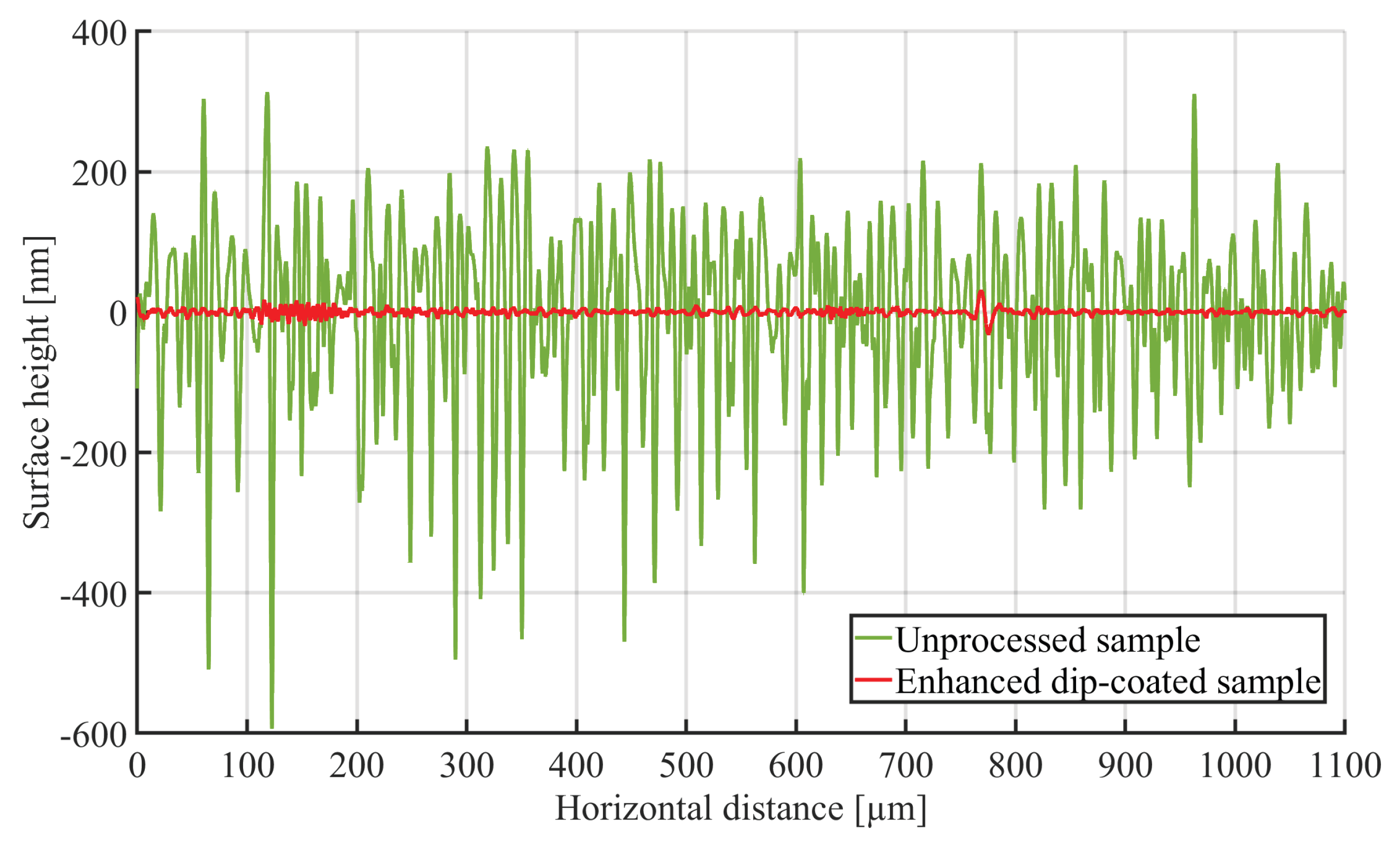
Figure A2.
Evaluation of surface roughness measurements of enhanced dip-coated (top) and unprocessed samples (bottom) along with the arithmetic mean surface height .
Figure A2.
Evaluation of surface roughness measurements of enhanced dip-coated (top) and unprocessed samples (bottom) along with the arithmetic mean surface height .
References
- Thompson, M.K.; Moroni, G.; Vaneker, T.; Fadel, G.; Campbell, R.I.; Gibson, I.; Bernard, A.; Schulz, J.; Graf, P.; Ahuja, B.; et al. Design for Additive Manufacturing: Trends, opportunities, considerations, and constraints. CIRP Annals 2016, 65, 737–760. [Google Scholar] [CrossRef]
- Berglund, G.; Wisniowiecki, A.; Gawedzinski, J.; Applegate, B.; Tkaczyk, T.S. Additive manufacturing for the development of optical/photonic systems and components. Optica 2022, 9, 623–638. [Google Scholar] [CrossRef]
- Shan, Y.; Hua, J.; Mao, H. 3D Printing of Optical Lenses Assisted by Precision Spin Coating. Advanced Functional Materials 2024, 34, 2407165. [Google Scholar] [CrossRef]
- Heinrich, A.; Rank, M. 3D printing of Optics; SPIE, 2018. [Google Scholar]
- Trunin, P.; Cafiso, D.; Beccai, L. Design and 3D printing of soft optical waveguides towards monolithic perceptive systems. Additive Manufacturing 2025, 100, 104687. [Google Scholar] [CrossRef]
- Elkaseer, A.; Chen, K.J.; Janhsen, J.C.; Refle, O.; Hagenmeyer, V.; Scholz, S.G. Material jetting for advanced applications: A state-of-the-art review, gaps and future directions. Additive Manufacturing 2022, 60, 103270. [Google Scholar] [CrossRef]
- Shrotri, A.; Beyer, M.; Stübbe, O. Manufacturing and analyzing of cost-efficient fresnel lenses using stereolithography. In Proceedings of the 3D Printed Optics and Additive Photonic Manufacturing II. International Society for Optics and Photonics, SPIE, 2020, Vol. 11349, p. 113490N. [CrossRef]
- Hua, J.; Shan, Y.; Wu, S.; Mao, H. Three-Dimensional Printed Diffraction Gratings Drop Coated by Different Resins and Their Mechanism. Journal of Manufacturing Science and Engineering 2023, 146, 011001. [Google Scholar] [CrossRef]
- Zhu, J.; Yang, Y.; Hu, N.; Liao, S.; Nulman, J. Additively Manufactured Multi-Material Ultrathin Metasurfaces for Broadband Circular Polarization Decoupled Beams and Orbital Angular Momentum Generation. ACS Applied Materials & Interfaces 2021, 13, 59460–59470. [Google Scholar] [CrossRef]
- Klenam, D.; McBagonluri, F.; Asumadu, T.; Osafo, S.; Bodunrin, M.; Agyepong, L.; Osei, E.; Mornah, D.; Soboyejo, W. Additive manufacturing: shaping the future of the manufacturing industry – overview of trends, challenges and opportunities. Applications in Engineering Science 2025, 22, 100224. [Google Scholar] [CrossRef]
- Golhin, A.P.; Tonello, R.; Frisvad, J.R.; Grammatikos, S.; Strandlie, A. Surface roughness of as-printed polymers: a comprehensive review. The International Journal of Advanced Manufacturing Technology 2023, 127, 987–1043. [Google Scholar] [CrossRef]
- Shrotri, A.; Mukherjee, A.K.; Lohöfener, S.; Springer, A.; Stübbe, O.; Preu, S. Additive manufacturing and characterization of hollow core metal and topas waveguides for Terahertz sensor systems. In Proceedings of the 2023 48th International Conference on Infrared, Millimeter, and Terahertz Waves (IRMMW-THz), 2023, pp. 1–2. [CrossRef]
- Beyer, M.; Shrotri, A.; Stübbe, O. Evaluation of stereolithography processes for the production of lens prototypes. In Proceedings of the Production Engineering and Management. TH OWL, 2019, Vol. 11349, pp. 227–239.
- Žigon, J.; Kariž, M.; Pavlič, M. Surface Finishing of 3D-Printed Polymers with Selected Coatings. Polymers 2020, 12. [Google Scholar] [CrossRef] [PubMed]
- Sarkar, A.K.; Sarmah, D.; Baruah, S.; Datta, P. An Optimized Dip Coating Approach for Metallic, Dielectric, and Semiconducting Nanomaterial-Based Optical Thin Film Fabrication. Coatings 2023, 13. [Google Scholar] [CrossRef]
- Rauh, F.; Bienek, O.; Sharp, I.D.; Stutzmann, M. Conversion of a 3D printer for versatile automation of dip coating processes. Review of Scientific Instruments 2023, 94, 083901. [Google Scholar] [CrossRef] [PubMed]
- Trinh, T.; Smihi, M.; Koev, L.; Zielinski, R. Dip Coating Process for Optical Elements, 2004. US Patent, US20040096577A1.
- Vaidya, N.; Solgaard, O. 3D printed optics with nanometer scale surface roughness. Microsystems & Nanoengineering 2018, 4, 18. [Google Scholar] [CrossRef]
- Evertz, A.; Schrein, D.; Olsen, E.; Hoffmann, G.A.; Overmeyer, L. Dip coating of thin polymer optical fibers. Optical Fiber Technology 2021, 66, 102638. [Google Scholar] [CrossRef]
- Shrotri, A.; Preu, S.; Stübbe, O. Achieving Transparency and Minimizing Losses of Rough Additively Manufactured Optical Components by a Dip-Coating Surface Finish. Coatings 2025, 15. [Google Scholar] [CrossRef]
- Ruchka, P.; Kushwaha, A.; Marathe, J.A.; Xiang, L.; Chen, R.; Kirk, R.W.; Tan, J.T.M.; Bursill, C.; Verjans, J.; Thiele, S.; et al. 3D-printed micro-axicon enables extended depth-of-focus intravascular optical coherence tomography in vivo. Advanced Photonics 2025, 7, 026003. [Google Scholar] [CrossRef]
- Kumar, P.; Martin, H.; Henning, A.; Jiang, J. Probing depth enhancements of spectral domain optical coherence tomography using axicons for the inspection of additively manufactured polymer parts. In Proceedings of the Proceedings of the Joint Special Interest Group meeting between euspen and ASPE, United Kingdom, sep 2023.
- Ahmed, M. 3D Printed Optical Components For THz-Spectroscopy. In Proceedings of the 3D Printed Optical Components For THz-Spectroscopy, Austria, March 2019. [Google Scholar]
- Khonina, S.N.; Kazanskiy, N.L.; Khorin, P.A.; Butt, M.A. Modern Types of Axicons: New Functions and Applications. Sensors 2021, 21. [Google Scholar] [CrossRef]
- Wei, X.; Liu, C.; Niu, L.; Zhang, Z.; Wang, K.; Yang, Z.; Liu, J. Generation of arbitrary order Bessel beams via 3D printed axicons at the terahertz frequency range. Appl. Opt. 2015, 54, 10641–10649. [Google Scholar] [CrossRef]
- Shrotri, A.; Joshi, S.; Vogel, L.; Starsaja, A.; Stübbe, O.; Preu, S. Terahertz Axicon Lenses. In Proceedings ofbthe 2025 50th International Conference on Infrared, Millimeter, and TerahertzWaves (IRMMW-THz), 2025, pp. 1–2. [CrossRef]
- Shi, L.; Dong, X.; Deng, Q.; Lu, Y.; Ye, Y.; Du, C. Design and characterization of an axicon structured lens. Optical Engineering 2011, 50, 063001. [Google Scholar] [CrossRef]
- Bachus, K.; de Lima Filho, E.S.; Wlodarczyk, K.; Oleschuk, R.; Messaddeq, Y.; Loock, H.P. Fabrication of axicon microlenses on capillaries and microstructured fibers by wet etching. Opt. Express 2016, 24, 20346–20358. [Google Scholar] [CrossRef]
- Shrotri, A.; Krause, B.; Stübbe, O.; Pfeiffer, U.; Preu, S. Evaluation of Additively Manufactured Axicon Lenses Using a THz-Camera. In Proceedings of the 2024 49th International Conference on Infrared, Millimeter, and Terahertz Waves (IRMMW-THz), 2024, pp. 1–2. [CrossRef]
- Jaroszewicz, Z. Axicons: Design and Propagation Properties; Research and Development Treatises, Polish Chapter of SPIE: Warsaw, 1997. [Google Scholar]
- González-Acuña, R.G.; Chaparro-Romo, H.A.; Gutiérrez-Vega, J.C. Analytical Lens Design; 2053-2563, IOP Publishing, 2020. [CrossRef]
- Brand, C.; Simonović, K.; Kiałka, F.; Troyer, S.; Geyer, P.; Arndt, M. A fiber-based beam profiler for high-power laser beams in confined spaces and ultra-high vacuum. Optics Express 2020, 28, 6164. [Google Scholar] [CrossRef]
- Levich, B.; Landau, L. Dragging of a liquid by a moving plate. Acta Physicochimica U.R. S. S., Vol. XVII, No 1942, XVII, 42–54.
- Maleki, M.; Reyssat, M.; Restagno, F.; Quéré, D.; Clanet, C. Landau–Levich menisci. Journal of Colloid and Interface Science 2011, 354, 359–363. [Google Scholar] [CrossRef] [PubMed]
- Jähne, B. Digitale Bildverarbeitung, 8 ed.; Springer Vieweg: Wiesbaden, Germany, 2024. [Google Scholar]
Figure 2.
Autodesk Fusion 360 screenshot depicting the 3D-representation (left) and 2D-sketch (right) of an axicon of apex angle 140°.
Figure 2.
Autodesk Fusion 360 screenshot depicting the 3D-representation (left) and 2D-sketch (right) of an axicon of apex angle 140°.
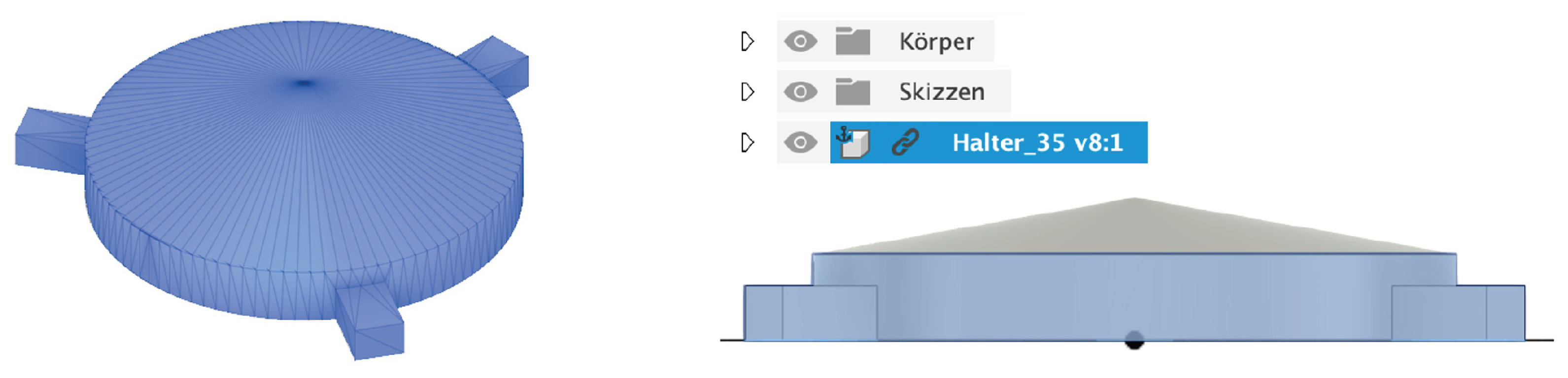
Figure 3.
Step-by-step enhanced dip-coating approach based on interval dipping and intermittent hardening.
Figure 3.
Step-by-step enhanced dip-coating approach based on interval dipping and intermittent hardening.
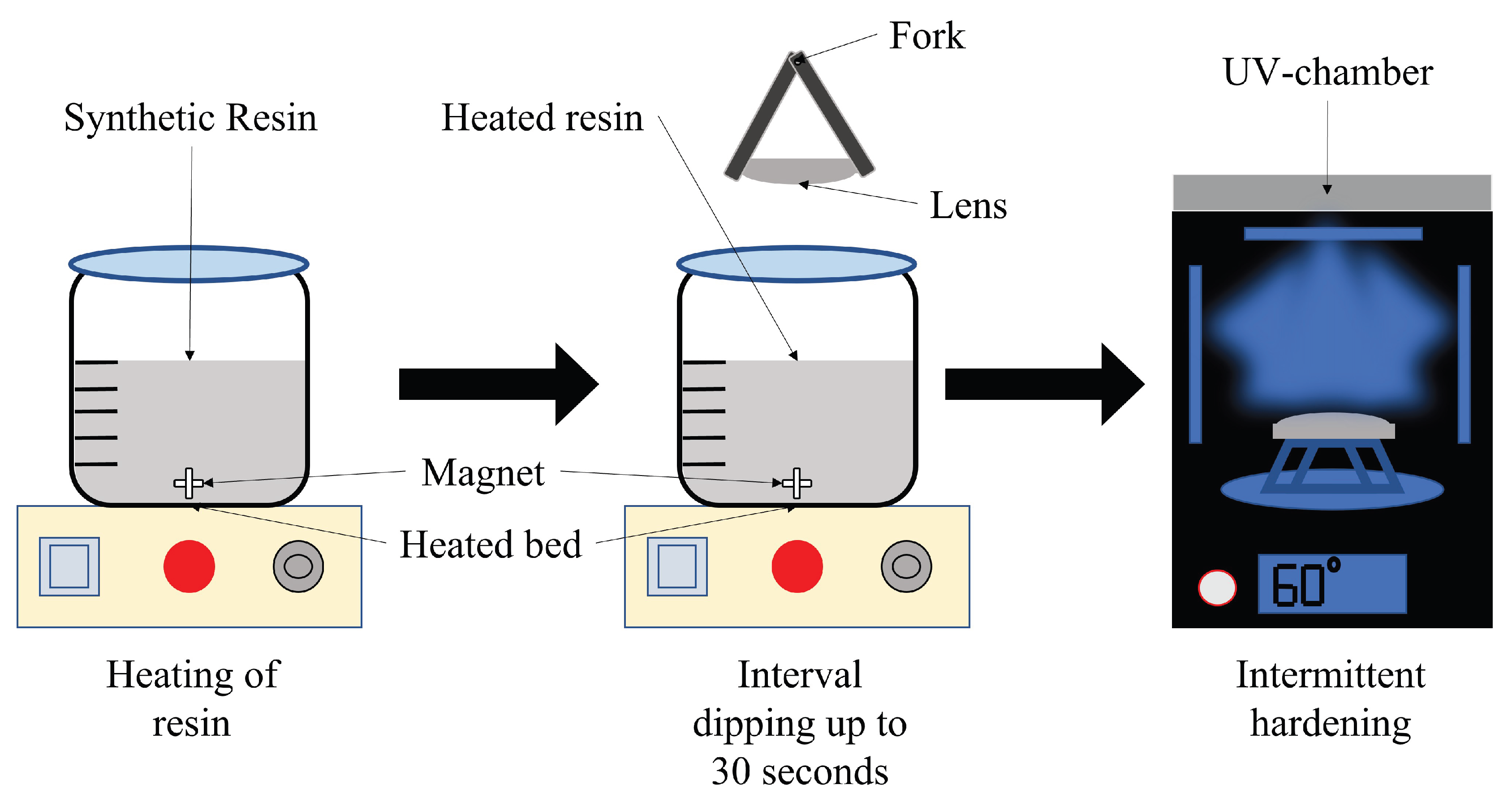
Figure 4.
Achieved transparency of a THz-axicon (microscope image) (top) and a NIR-axicon (bottom) before and after enhanced dip-coating depicting the unprocessed (left) and enhanced dip-coated (right) axicon samples.
Figure 4.
Achieved transparency of a THz-axicon (microscope image) (top) and a NIR-axicon (bottom) before and after enhanced dip-coating depicting the unprocessed (left) and enhanced dip-coated (right) axicon samples.
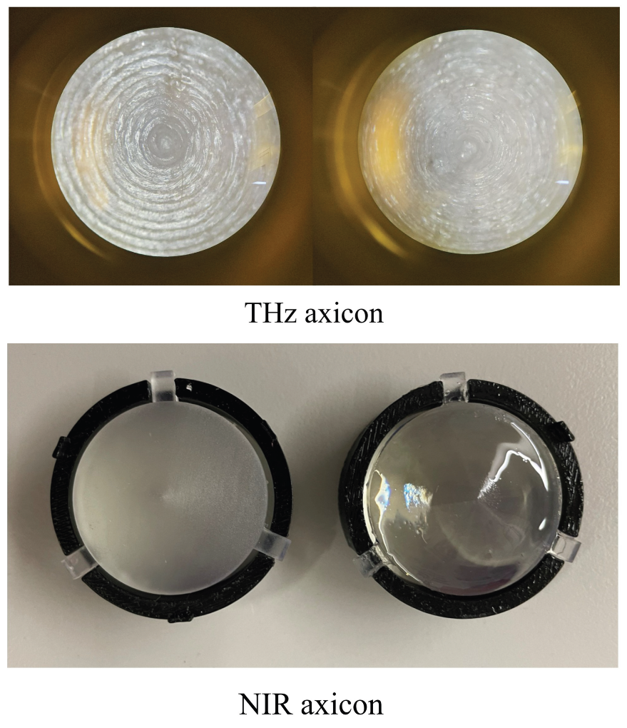
Figure 5.
Normalized intensity distribution of the unprocessed (left) and dip-coated (right) axicons in the frequency range of 100 - 200 at distances 55 and 82 from the receiver [26].
Figure 5.
Normalized intensity distribution of the unprocessed (left) and dip-coated (right) axicons in the frequency range of 100 - 200 at distances 55 and 82 from the receiver [26].
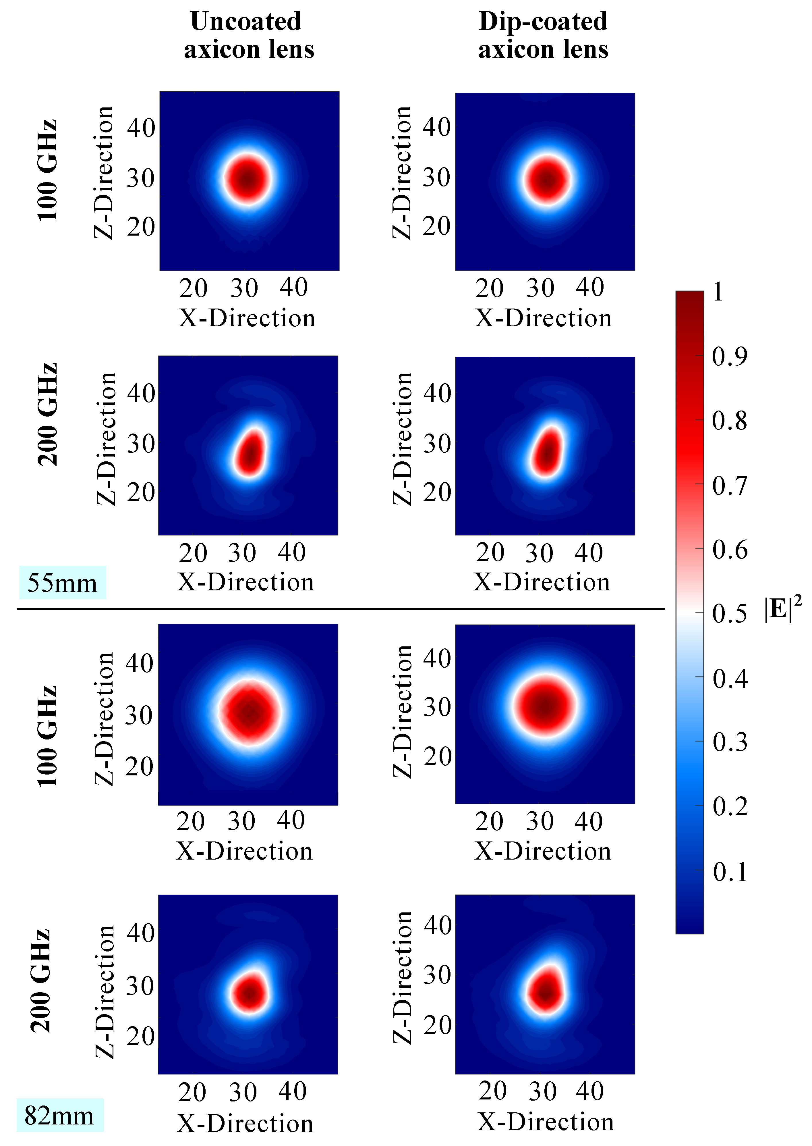
Figure 6.
Experimental setup for the measurement of the beam profile of an axicon at 1550 nm.
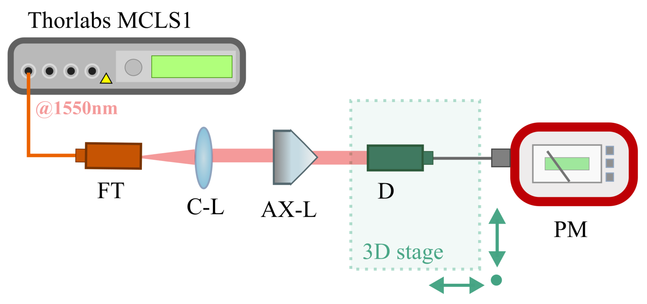
Figure 7.
Beam profile of NIR axicons with an apex angle of 140°.
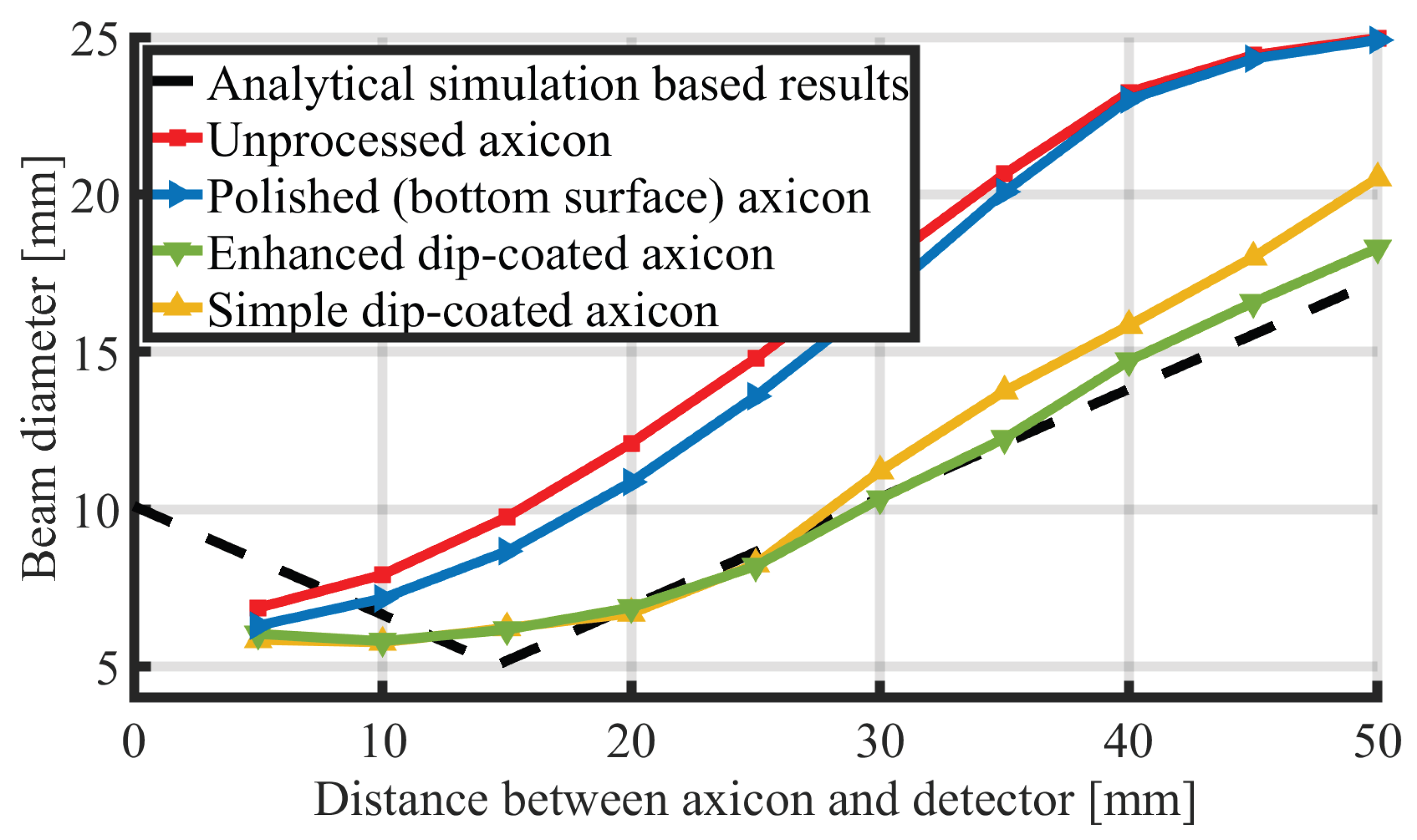
Figure 8.
Integrated optical power at different distances to estimate the DOF region of NIR axicons with an apex angle of 140°.
Figure 8.
Integrated optical power at different distances to estimate the DOF region of NIR axicons with an apex angle of 140°.
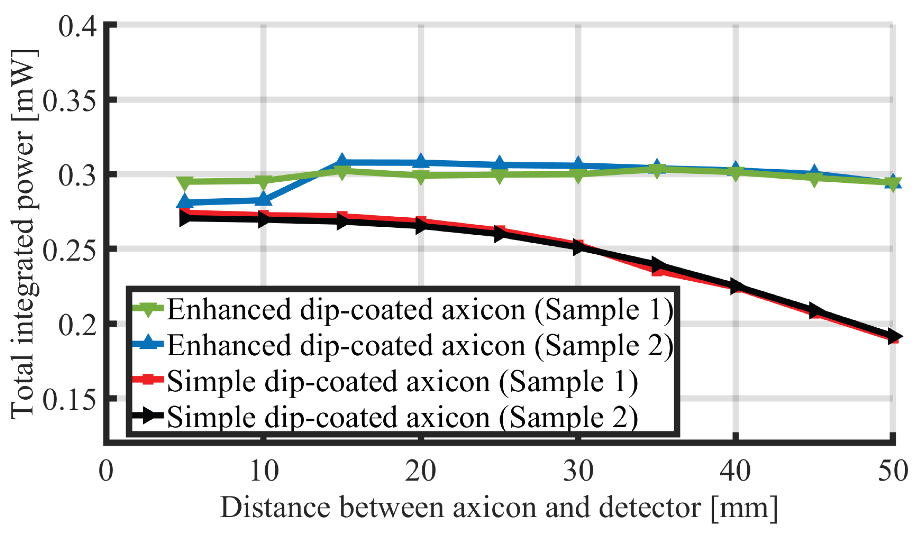
Figure 9.
Beam profile of NIR axicons with an apex angle of 150° (top) and 160° (bottom).
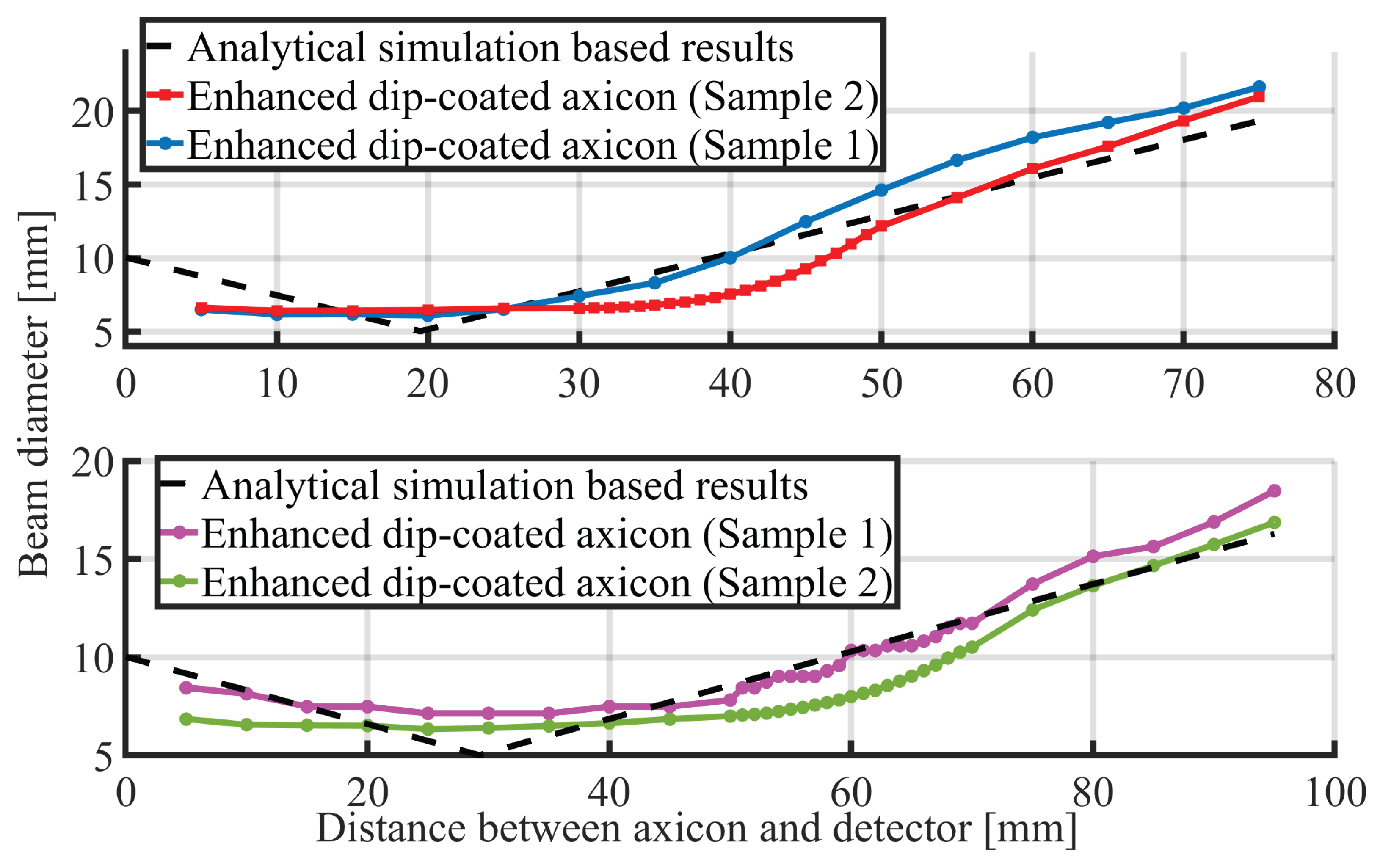

Table 1.
Design parameters of NIR and THz axicons.
| Apex angle () | Cone angle () | h | DOF (NIR) | DOF (THz) |
|---|---|---|---|---|
| 140° | 20° | |||
| 150° | 15° | |||
| 160° | 10° |
Table 2.
Comparison of surface roughness after applying simple dip-coating and enhanced dip-coating based post-processing.
Table 2.
Comparison of surface roughness after applying simple dip-coating and enhanced dip-coating based post-processing.
| Post-processing technique | Simple dip-coating | Enhanced dip-coating |
|---|---|---|
| Roughness () | 5 | up to 3 |
Disclaimer/Publisher’s Note: The statements, opinions and data contained in all publications are solely those of the individual author(s) and contributor(s) and not of MDPI and/or the editor(s). MDPI and/or the editor(s) disclaim responsibility for any injury to people or property resulting from any ideas, methods, instructions or products referred to in the content. |
© 2026 by the authors. Licensee MDPI, Basel, Switzerland. This article is an open access article distributed under the terms and conditions of the Creative Commons Attribution (CC BY) license (http://creativecommons.org/licenses/by/4.0/).
Copyright: This open access article is published under a Creative Commons CC BY 4.0 license, which permit the free download, distribution, and reuse, provided that the author and preprint are cited in any reuse.


