Submitted:
29 January 2026
Posted:
30 January 2026
You are already at the latest version
Abstract
This work demonstrates an efficient and reproducible method for the covalent biofunctionalization of epoxy solder mask surfaces on printed circuit boards (PCBs) produced using a conventional manufacturing process, enabling the implementation of capacitive biosensors without the need for any additional PCB fabrication steps and thereby supporting low-cost biosensing applications. Surface activation was achieved using 600 mM 3-mercaptopropionic acid (3-MPA) and 600 mM EDC/NHS, followed by immobilization of 600 µM bovine serum albumin (BSA) as a model protein, achieving spatial variability below 10%. This methodology can be directly applied to other proteins by simply substituting the biomolecule of interest. ATR-FTIR analysis confirmed successful chemical modification through the appearance of characteristic carboxyl and amide bands, while BCA assays verified effective protein attachment. The sensing performance of the functionalized surface was evaluated using electrochemical impedance spectroscopy on interdigitated PCB-based electrodes. A clear decrease in the impedance module was observed at 1 MHz after BSA immobilization and subsequent anti-BSA binding with a variation of 2826 ± 235 Ω and 4214 ± 239 Ω respectively (p < 0.001). Remarkably, anti-BSA was detected at concentrations as low as 10 ppb. These results highlight not only the strong biochemical activity and stability of the modified solder mask surface, but also its potential for scalable, robust, and cost-effective PCB-integrated biosensors for clinical biomarker detection and point-of-care diagnostics, as well as other widespread diagnostic and sensing applications.
Keywords:
biofunctionalization
; impedance
; printed circuit board (PCB)
; solder mask
1. Introduction
Printed Circuit Boards (PCBs) are a key component of nearly all modern electronic devices, providing a rigid platform that supports and interconnects electronic components. By enabling miniaturization, reliability, and high-density circuitry, PCBs have been essential to the rapid advancement of electronics technology. The invention of the PCB is credited to Austrian engineer Paul Eisler, who developed the first prototype in England in 1936 [1]. Widespread commercial adoption followed in the United States during the post–World War II era, particularly by the mid-1950s. Over time, PCBs have evolved from simple, single-sided boards using through-hole mounting to sophisticated multilayer structures with surface-mount technology (SMT), driving developments in consumer electronics, industry, and aerospace.
A key innovation in this evolution was the transition from point-to-point wiring and through-hole assembly to SMT between the 1960s and 1980s. This shift allowed for significant miniaturization of components, automation of assembly processes, higher circuit density, and lower production costs. Modern PCBs now commonly feature one to sixteen copper layers separated by dielectric substrates such as FR-4, and may include advanced features like blind, buried, or through-vias to facilitate complex routing.
Among the essential features of PCB design, yet sometimes underrated, is the need of a solder mask. The solder mask is a protective polymer coating applied over copper traces, exposing only the solder pads. Its primary functions are to prevent oxidation of copper, protect against mechanical damage, and control the flow of solder during manufacturing. Importantly, the solder mask contributes to signal integrity in multilayer and high-frequency designs by reducing capacitive coupling between adjacent traces. A notable class of solder mask material is based on epoxy resins, which are thermosetting polymers renowned for excellent thermal stability, chemical resistance, and mechanical strength. Synthesized from phenol and formaldehyde, Novolac resins’ highly cross-linked structure enables them to endure high temperatures and harsh conditions, making them ideal for demanding PCB applications. Moreover, in solder mask formulations, epoxies improve adhesion to copper and substrates, enhance resistance to thermal cycling during soldering, and maintain electrical insulation even in challenging environments. These attributes make these resins a preferred choice in advanced and high-reliability electronics manufacturing.
Beyond their material properties, the versatility and robustness of PCBs, particularly when combined with these epoxy-based solder masks, have enabled their use as adaptable substrates for diverse applications [2]. The evolution from single- to multilayer configurations, and later to flexible PCBs, has broadened their applicability across industries such as telecommunications, aerospace, and increasingly, biomedical engineering. Their structural adaptability and precision manufacturing make them suitable not only for conventional electronics but also for integrating actuators, coils, microheaters, and other components into complex microelectromechanical systems.
In recent years, the integration of PCB technology in sensor development has expanded considerably. By exploiting its multilayer design and standardized photolithographic fabrication, PCBs allow the patterning of highly reproducible electrodes with controlled geometry and spacing, crucial for the miniaturization of electrochemical sensors [2,3]. Their combination of electrical reliability and mechanical stability supports applications in environmental monitoring, chemical analysis, and medical diagnostics. Flexible PCB substrates, typically based on polyimide, further extend this capability to dynamic and wearable environments, providing conformability and durability under mechanical stress. These features have stimulated the design of integrated systems that merge electronics with microfluidics, creating cost-effective and portable sensors with real-time data acquisition [4,5,6].
The transition of PCB technology into biosensing represents a major paradigm shift, bridging traditional electronics with bioanalytical chemistry. As noted by Mahapatra et al. [7] PCBs now function not only as electronic backbones but also as active sensing matrices capable of supporting biochemical reactions and transducing biological signals. Their integration with microcontroller units (MCUs) and wireless communication modules has led to automated and miniaturized electrochemical workstations (potentiostats). These advances have enabled the development of open-source, portable biosensing devices that support electrochemical and optical detection of biomolecules with high sensitivity, reproducibility, and multiplexing capabilities. [8,9].
Recent innovations demonstrate the convergence of PCB-based microfabrication and molecular diagnostics in Lab-on-PCB (LoP) systems. LoP devices integrate microfluidics, sensors, and actuators on a single PCB platform, offering rapid, automated analyses using minimal sample volumes. The LoCKAmp platform exemplifies this integration [10], achieving virus genetic detection in under three minutes through on-chip amplification and signal readout.
Capacitive biosensors have attracted increasing attention in recent years and constitute a widely used label-free electrochemical transduction approach for biomolecular detection. These devices detect biomolecular interactions by monitoring variations in electrical capacitance caused by specific binding events on functionalized electrode surfaces [11,12]. According to the review by Weaver et al. [13], the behavior of the capacitance in such sensors depends on numerous factors. In some instances, the presence of the analyte produces an increase in capacitance [14,15,16,17], whereas in others the capacitance value decreases [18,19,20,21]. Some of the factors that influence biosensor capacitance include the type and size of the analyte, the size and geometry of the electrodes, and the insulation/immobilization chemistry [22]. Preferred recognition elements for capacitive sensors include antibodies, aptamers, and proteins [11]. In certain configurations the electrodes are covered by an insulating layer prior to functionalization, whereas in others the electrodes are functionalized directly [23,24]. The presence of a dielectric coating separating the electrodes from the sample medium is generally associated with improved signal stability and reduced interference, compared to configurations where the electrodes are directly exposed to the environment.
Although several methods exist to measure capacitance accurately [25], electrochemical impedance spectroscopy (EIS) remains the most widely adopted technique for characterizing capacitive biosensors, owing to its ability to resolve dielectric modulation, interfacial charge distribution, and surface polarization dynamics in real time [13,26,27,28].
Although the structural and electrical properties of PCBs make them a cost-effective and scalable platform for biosensing applications, in many cases the direct implementation of sensors on the PCB requires materials—such as gold—that are not part of the standard PCB manufacturing process, thereby forcing either post-processing of the board after fabrication or the inclusion of additional steps in the PCB fabrication workflow to deposit specific metallic coatings [29]. Moreover, when gold layers are applied using common PCB finishes such as electroless nickel immersion gold (ENIG), the resulting gold coating may not meet the required purity and quality standards [30]. In ENIG, gold is deposited over an electroless nickel barrier layer that itself lies on copper. As a result, the functional gold surface can be indirectly influenced by the underlying nickel - and, through it, by the copper substrate - due to factors such as limited gold thickness, porosity, and interdiffusion. These effects can adversely affect electrical performance, chemical stability, and long-term reliability in biosensing applications. In this work, we present an alternative approach for implementing capacitive biosensors by rendering the outermost PCB surface - the solder mask - selective to the target analyte through its functionalization. This approach would allow the insulating layer of a capacitive biosensor to be obtained directly from the standard PCB manufacturing process, without the need for additional deposition or printing steps. Therefore, the aim of this study is to demonstrate that an epoxy solder mask can be modified to create surfaces that specifically interact with chosen biological targets. As a proof of concept, we explore the attachment of bovine serum albumin (BSA) onto the solder mask and evaluate the specific recognition of anti-BSA antibodies, noting that this functionalization strategy provides a versatile platform that can be readily adapted to other proteins or biomolecular targets. The functionalization and its effect on the sensing properties were assessed using interdigitated electrodes as capacitive sensor and EIS as measurement method.
2. Materials and Methods
For the characterization of the functionalization on the solder mask surface, simple interdigitated sensors implemented on PCBs and covered with solder mask were employed. The sensor design was carried out using the open-source software KiCAD. The layout and dimensions of the sensors are shown in Figure 1. The interdigitated sensor consists of two electrodes with eight digits each. Each digit has a width of 100 µm and a length of 270 µm, with an interdigit spacing of 100 µm.
Once designed, the sensors were fabricated by Eurocircuits NV (Mechelen, Belgium). According to the manufacturer, the thickness of the copper interdigitated electrodes is approximately 35 µm, while the thickness of the soldermask layer is at least 7 µm across the entire electrode surface.
Before the functionalization process, epoxy resin pieces (chips, ca 0,5 cm x 0,5 cm) were attained from interdigitated electrodes, cleaned with an air flow and then characterized by Attenuated Total Reflection-Fourier Transform Infrared (ATR-FTIR) to establish baseline surface properties. Spectra were collected with a Bruker (Massachusetts, USA) Tensor-27 spectrometer, equipped with a diamond ATR crystal.
Surface activation was performed at room temperature, under an inert atmosphere and in darkness, by immersing the chips 24 hours in freshly prepared solutions of 3-mercaptopropionic acid (3-MPA) purchased from Sigma-Aldrich (St. Louis, Missouri, USA) with a purity of ≥99%. After activation, the chips were thoroughly rinsed with ultrapure water, dried under an air stream, and re-characterized by ATR-FTIR to assess surface modifications. Subsequently, the chips were incubated for one hour with gentle stirring and darkness in a solution containing N-ethyl-N’-(3-dimethylaminopropyl) carbodiimide (EDC) from Merck (Darmstadt, Germany) and N-hydroxysuccinimide (NHS) from Sigma-Aldrich. Following activation, surfaces were functionalized by immersion for one hour at room temperature, with gentle stirring and in darkness, in a BSA (from Merck) solution prepared in a 50 mM carbonate-bicarbonate buffer (both from Sigma-Aldrich) at pH 9.6 using ultrapure water. All solutions were prepared daily using ultrapure water (resistivity 18.2 MΩ·cm at 25°C) obtained from a Smart2Pure3 water purification system (Thermo Electron LED GmbH, Langenselbold, Germany).
After incubation, the chips were thoroughly rinsed with carbonate buffer and dried using air before analysis by ATR-FTIR to confirm successful protein immobilization. Protein binding was further verified using a colorimetric bicinchoninic acid (BCA) assay kit (Thermo Fisher Scientific, Waltham, Massachusetts, USA). The development of a purple color on the surface indicated a positive interaction between the immobilized BSA and the functionalized PCB substrate.
To characterize the functionalization, impedance spectroscopy measurements were performed in the frequency range of 10 kHz to 1 MHz, using a sinusoidal signal amplitude of 100 mV. The measurements were conducted using a PalmSens4 potentiostat/galvanostat/impedance analyzer (PalmSens BV, Houten, Netherlands).
The recognition experiments were conducted in a 10 ppb solution of Anti-BSA antibody produced in rabbit, purchased from Sigma-Aldrich (Saint Louis, MO, USA), prepared in phosphate-buffered saline buffer (PBS pH 7.4, made with sodium chloride 137 mM, potassium chloride 3 mM, disodium phosphate 8 mM and monopotassium phosphate 1 mM, all from Sigma-Aldrich). To asses the variability associated with PCB fabrication and surface functionalization, three independent sensors were characterized. First, impedance spectroscopy measurements were performed on the three unfunctionalized sensors, with three repetitions for each sensor. After functionalization, the impedance spectroscopy measurements were repeated, again performing three repetitions per sensor. Subsequently, each sensor was immersed in the Anti-BSA solution for 20 minutes. Finally, after immersion, three additional impedance spectroscopy measurements were conducted for each of the three sensors. All the impedance spectroscopy measurements were done in PBS.
3. Results and Discussion
Taking advantage of the well-known chemical stability and reactive backbone of epoxy resins, this work uses these materials to introduce functional groups onto the surface of PCB circuits. Functionalizing a solder mask through covalent bonding involves modifying its surface or composition so that specific functional groups are stable and permanently attached to the polymer matrix. For this purpose, bare PCB surfaces coated with epoxy resin were first characterized by ATR-FTIR spectroscopy (Figure 2). The ATR-FTIR spectrum of the untreated PCB surface displays several characteristic absorption bands that align with the expected structure of the resin. A band in the 3300–3500 cm⁻¹ region is observed, corresponding to O–H stretching vibrations of free hydroxyl groups. Its low intensity may indicate that the resin has undergone a high degree of curing. The broad peaks around 2900 cm⁻¹ correspond to C–H stretching vibrations of aliphatic –CH₂– and –CH₃ groups, typical of epoxy resins. A distinct band around 1725 cm⁻¹ is attributed to C=O stretching vibrations of carbonyl groups as a result of using anhydrides as curing agents. The peaks around 1450 cm⁻¹ are associated with C–H bending (scissoring) vibrations of methylene groups, as well as stretching vibrations of the aromatic ring skeleton. A strong band around 1010 cm⁻¹ corresponds to C–O stretching from ether linkages and may include contributions from epoxide ring vibrations. Additionally, a shoulder observed around 1100 cm⁻¹ is attributed to the asymmetric C–O–C stretching vibrations, characteristic of the epoxy matrix. In the fingerprint region, below 800 cm⁻¹, several overlapping bands are present, including out-of-plane C–H bending modes from substituted aromatic rings, and other deformations characteristic of the epoxy. These features confirm the presence of an epoxy resin coating on the PCB surface prior to chemical functionalization.
Once characterized, the surface of the epoxy resin was incubated for 24 hours with a dilution of 3-MPA, a small molecule containing a thiol group (–SH) with strong nucleophilicity, to promote molecular self-assembly on the surface and thus form a uniform monolayer. This thiol group reacts selectively with the epoxide rings present on the resin surface, opening the rings and leading to the covalent attachment of –3-MPA. As a result, carboxylic acid groups (–COOH) are introduced onto the surface, providing functional handles for further chemical modifications. As explained in the Materials and Methods section, EDC is then used to activate carboxylic groups by forming a transient O-acylisourea intermediate, which is then stabilized by NHS through the formation of an NHS ester. This highly reactive ester readily forms stable amide bonds with primary amine groups, allowing for efficient and specific biofunctionalization of the resin surface.
To verify the occurrence of the chemical reaction, Figure 2 shows the ATR-FTIR spectra of the epoxy resin after 24 hours treatment with 3-MPA at a concentration of 1000 mM. As expected, the spectra display an intensified band in the 3300–3500 cm⁻¹ region, corresponding to the O–H stretching vibrations of carboxylic acid hydroxyl groups, together with a stronger band in the 1700–1725 cm⁻¹ region, associated with the C=O stretching vibrations of the same functional groups. These features confirm the incorporation of the COOH group from 3-MPA onto the resin surface.
Since the absorption band around 1725 cm⁻¹ provides the clearest signal for identifying the presence of 3-MPA on the surface, this wavenumber is selected as the reference for evaluating the optimal 3-MPA concentration for resin functionalization. Figure 3 shows the plot of the intensity of this band as a function of 3-MPA concentration. In this figure, it can be observed that the untreated surface exhibits only a weak signal in this region. Upon 24 hours incubation with 3-MPA, a well-defined and statistically significant peak appears, increasing in intensity up to 600 mM. Beyond this concentration, however, the signal progressively decreases, reaching its minimum at the highest concentration tested (pure 3-MPA), suggesting that excessive 3-MPA may reduce the efficiency of surface functionalization.
This trend is consistent with the known behavior of 3-MPA in aqueous solutions, where it tends to form dimers through hydrogen bonding interactions between carboxylic reactivity and availability of functional groups, potentially limiting the interaction between 3-MPA and the epoxide groups on the resin surface.
Based on these results, 600 mM was identified as the optimal 3-MPA concentration for functionalizing the epoxy resin surface. This step is crucial, as it defines the density of carboxyl groups introduced onto the PCB surface, these being the exclusive reactive sites for subsequent activation and covalent coupling. Since each carboxyl group introduced by 3-MPA is converted into an NHS-ester intermediate using EDC and NHS, the 3-MPA concentration directly determines the amount of activating agents needed for efficient surface functionalization Consequently, 600 mM will be used as the standard concentration in the next step involving EDC/NHS activation. At this concentration, a sufficient number of carboxyl groups are generated, ensuring efficient activation by EDC/NHS and maximizing the potential for covalent attachment of biomolecules.
Figure 4 shows the ATR-FTIR spectrum of the epoxy resin after covalent immobilization of BSA, following the procedure detailed in the Materials and Methods section, using concentrations of 600 mM for 3-MPA, EDC/NHS, and BSA at 600 µM. The spectrum exhibits characteristic protein absorption bands around 1650 cm⁻¹ and 1540 cm⁻¹, corresponding to the amide I (mainly C=O stretching) and amide II (N–H bending and C–N stretching) vibrations, respectively. A broad band around 3289 cm⁻¹ is also observed, attributed to N–H and O–H stretching from amino acid residues. The presence of these bands confirms the successful covalent attachment of the protein to the epoxy resin surface.
To further assess the functionalization process, the intensity of these characteristic bands was analyzed to evaluate the homogeneity of protein immobilization on the surface. For this purpose, ATR-FTIR signal intensities were measured at three different locations on nine independently functionalized resin chips. The relative deviation of the absorbance values was then calculated for each plate, yielding an average variation of 8±3% under different experimental conditions. Hence, the covalent immobilization of the protein onto the epoxy resin surface is achieved with good spatial uniformity using the described methodology.
The presence of covalently immobil”zed ’rotein on the resin surface was further confirmed using the BCA colorimetric assay, which detects protein content through the formation of a purple complex between bicinchoninic acid and cuprous ions generated by the reduction of copper ions via peptide bonds. An intense purple coloration was observed in the BCA assay solution for the functionalized resin, confirming successful protein attachment, see Figure 5. These results also demonstrate that, under the tested conditions, the epoxy resin surface was effectively biofunctionalized with BSA, as no development of the characteristic intense purple color was observed in the assay solution for the non-functionalized resin.
These results indicate that the optimal conditions for covalent immobilization of BSA onto the epoxy resin surface involve a 24 hours incubation with 600 mM 3-MPA, followed by activation with 600 mM EDC/NHS for 1 hour, and subsequent exposure of the surface to 600 µM BSA for 1 hour. The difference between these concentrations is mainly because BSA is roughly 1000 times larger than the MPA or EDC molecules. Under these conditions, the highest protein signal was achieved, confirming the most efficient covalent anchoring of BSA onto the functionalized resin. Other functionalization strategies were also tested, such as the 1,1’-carbonyldiimidazole method in organic solvent, but they yielded no results since the organic solvents employed degraded the epoxy resin.
Next, Figure 6 presents the impedance spectroscopy measurements performed in PBS for the three sensors (S1, S2 and S3) in their three states. The values shown correspond to the average of three independent measurement repetitions performed for each sensor in each state. For all devices, the impedance magnitude of the non-functionalized/bare sensors (B) is higher than that of the functionalized ones (F), which in turn slightly exceeds the response of the functionalized sensors after analyte recognition (A). We attribute this decrease in the impedance magnitude – that corresponds to an increase in the capacitance – to the formation of a charged dipolar interface during probe immobilization, and subsequently during the specific binding event between BSA and anti-BSA. The emergence of this interface alters the dielectric environment at the electrode–electrolyte boundary, and the dipole moment of the immobilized and bound biomolecular layer contributes to increased overall capacitance [13].
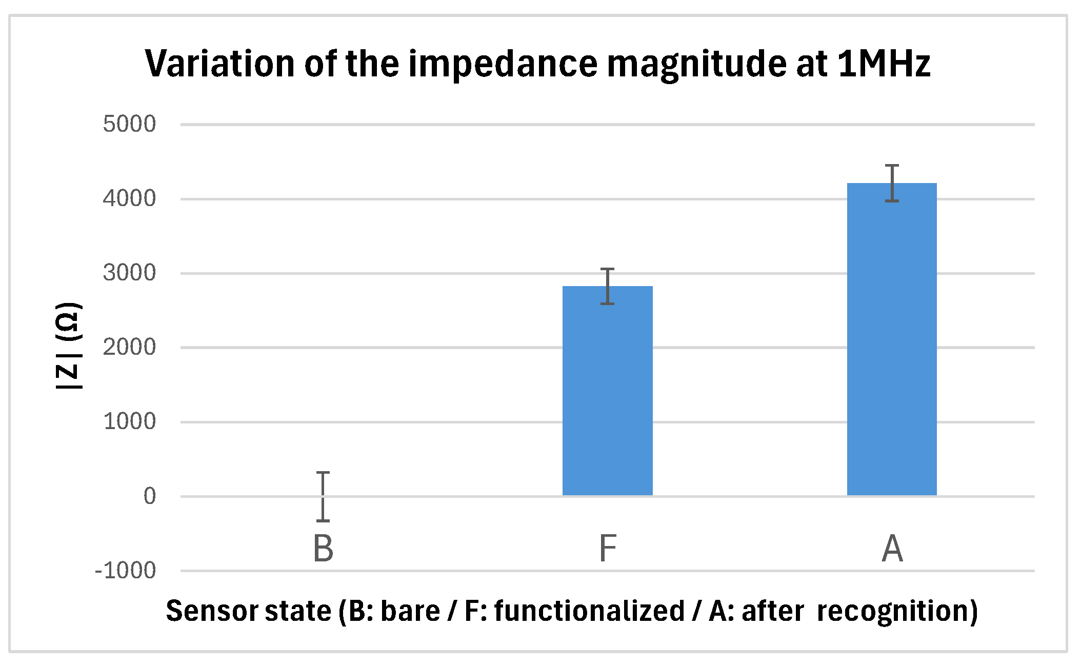
To numerically evaluate the effect of sensor functionalization and analyte recognition on the impedance magnitude, the impedance modulus at 1 MHz was extracted for each sensor. The mean value and standard deviation were then calculated for the three sensor states: non-functionalized/bare (B), functionalized (F), and after analyte recognition (A).
For the bare state, the difference of each measurement from the mean of the three repetitions was determined for each sensor. These differences were then averaged for each sensor, and the corresponding standard deviation was computed. Subsequently, the overall mean and standard deviation were obtained by averaging across the three sensors.
For the functionalized and analyte-recognized states, the mean impedance magnitude of the three repetitions was first calculated for each sensor. The relative change in impedance magnitude for each sensor was then calculated by subtracting the mean value of the functionalized or analyte-recognized sensor from the mean impedance magnitude of the corresponding bare sensor (bare - functionalized or bare - analyte-recognized). Finally, the average of these differences across the three sensors and the associated standard deviation were computed. Figure 7 shows the bar plot of the average difference and standard deviation of the sensors in the three states. For completeness, the bare state - whose mean difference is zero by definition but still exhibits a finite standard deviation - is also included.
Taking the bare sensor as the reference (mean impedance magnitude = 0 Ω, SD = 326 Ω), the functionalized sensor exhibited a mean relative impedance of 2826 ± 235 Ω. Upon exposure to the analyte, the impedance difference further increased to 4214 ± 239 Ω, corresponding to an additional rise of more than 1000 Ω compared with the functionalized sensor without analyte. These results demonstrate that the functionalization process induces a significant modification in the sensor’s electrical properties and that the functionalized surface enables specific recognition of the target analyte.
A one-way ANOVA was performed to compare the impedance values of the three experimental conditions: blank, functionalized surface, and functionalized surface with analyte. The analysis revealed a highly significant effect of the treatment on impedance values, F(2, 24) around 700, p < 0.001, indicating that all three groups differ statistically from each other. Post hoc comparisons confirmed that the impedance magnitude for both the functionalized and the functionalized + analyte conditions was significantly lower than that of the blank, with the recognition of the analyte further decreasing the signal. The statistical detection of this low concentration (10 ppb) of anti-BSA underscores the remarkable sensitivity achievable using low-cost PCBs directly, without requiring any additional steps beyond the standard fabrication process, thereby opening the door to highly scalable and reliable biosensing platforms.
4. Conclusions
The present work demonstrates that the surface of the epoxy solder mask used in standard PCB manufacturing can be successfully functionalized to enable covalent immobilization of biomolecules. Using 3-MPA as a coupling agent, carboxylic groups were introduced onto the epoxy surface, subsequently activated through EDC/NHS chemistry to form amide bonds with primary amines of BSA. ATR-FTIR characterization confirmed the appearance of characteristic absorption bands corresponding to carboxyl and amide functional groups, while BCA colorimetric assays verified the effective attachment of proteins. The optimized procedure, involving 600 mM 3-MPA and 600 µM BSA, resulted in efficient and homogeneous biofunctionalization of the epoxy surface with a spatial variation below 10%. Importantly, this functionalization methodology is highly versatile and can be readily applied to other proteins, providing a straightforward route to generate PCB-based sensors customized for different biomolecular targets.
To validate the functionalized solder mask as a sensing interface, electrochemical impedance spectroscopy (EIS) measurements were carried out on interdigitated capacitive sensors fabricated with PCB technology, where the solder mask acted as the dielectric insulating layer. The impedance spectra were recorded before functionalization, after BSA immobilization, and following analyte recognition (anti-BSA binding). The results revealed a clear decrease in impedance magnitude at 1 MHz-2826 ± 235 Ω after functionalization and over 1000 Ω after analyte recognition, 4214 ± 239 Ω -indicating an increase in capacitance consistent with the formation of charged dipolar interfaces during molecular binding events, F(2, 24) around 700, p < 0.001.
Overall, these findings highlight the potential of the solder mask in standard PCB substrates to serve not only as a structural and protective dielectric layer but also as a chemically active interface suitable for biofunctionalization. This approach enables the direct implementation of capacitive biosensors on conventionally fabricated PCBs, eliminating the need for additional deposition, printing, or screen-printing steps. Consequently, this strategy streamlines fabrication, lowers costs and processing complexity, and facilitates the scalable production of miniaturized, reliable, and application-specific PCB-integrated capacitive biosensors for applications such as clinical biomarker detection and point-of-care diagnostics.
Author Contributions
All authors contributed equally to all aspects of this work, including conceptualization, methodology, investigation, writing, and review. All authors have read and agreed to the published version of the manuscript.
Funding
This research was funded by the Spanish Ministry of Science and Innovation under grant PID2021-126304OB-C44 and the Spanish Ministry of Science, Innovation and Universities under grant PID2024-155683OB-C44.
Conflicts of Interest
The authors declare no conflicts of interest.
Abbreviations
The following abbreviations are used in this manuscript:
| PCB | Printed Circuit Board |
| SMT | Surface-mount technology |
| MCU | Microcontroller unit |
| LoP | Lab-on-PCB |
| EIS | Electrochemical impedance spectroscopy |
| ENIG | Electroless nickel immersion gold |
| ATR-FTIR | Attenuated total reflection-fourier transform infrared |
| 3-MPA | 3-mercaptopropionic acid |
| EDC | N-ethyl-N’-(3-dimethylaminopropyl) carbodiimide |
| NHS | N-hydroxysuccinimide |
| BSA | Bovine serum albumin |
| BCA | Bicinchoninic acid |
| PBS | Phosphate-buffered saline buffer |
| B | Bare sensor, non-functionalized |
| F | Functionalized sensor |
| A | Sensor after analyte recognition |
References
- Khandpur, R.S. Printed Circuit Boards Design, Fabrication and Assembly; 2006. [Google Scholar]
- Perdigones, F.; Quero, J.M. Printed Circuit Boards: The Layers’ Functions for Electronic and Biomedical Engineering. Micromachines (Basel). 2022, 13. [Google Scholar] [CrossRef] [PubMed]
- Shamkhalichenar, H.; Bueche, C.J.; Choi, J.W. Printed Circuit Board (PCB) Technology for Electrochemical Sensors and Sensing Platforms. Biosensors (Basel). 2020, 10. [Google Scholar] [CrossRef] [PubMed]
- Xu, C.; Song, Y.; Sempionatto, J.R.; Solomon, S.A.; Yu, Y.; Nyein, H.Y.Y.; Tay, R.Y.; Li, J.; Heng, W.; Min, J.; et al. A Physicochemical-Sensing Electronic Skin for Stress Response Monitoring. Nat. Electron. 2024, 7. [Google Scholar] [CrossRef] [PubMed]
- Rose, D.P.; Ratterman, M.E.; Griffin, D.K.; Hou, L.; Kelley-Loughnane, N.; Naik, R.R.; Hagen, J.A.; Papautsky, I.; Heikenfeld, J.C. Adhesive RFID Sensor Patch for Monitoring of Sweat Electrolytes. IEEE Trans. Biomed. Eng. 2015, 62. [Google Scholar] [CrossRef]
- Min, J.; Tu, J.; Xu, C.; Lukas, H.; Shin, S.; Yang, Y.; Solomon, S.A.; Mukasa, D.; Gao, W. Skin-Interfaced Wearable Sweat Sensors for Precision Medicine. Chem. Rev. 2023, 123, 5049–5138. [Google Scholar] [CrossRef]
- Mahapatra, S.; Kumari, R.; Chandra, P. Printed Circuit Boards: System Automation and Alternative Matrix for Biosensing. Trends Biotechnol. 2024, 42. [Google Scholar] [CrossRef]
- Shao, Y.; Ying, Y.; Ping, J. Recent Advances in Solid-Contact Ion-Selective Electrodes: Functional Materials, Transduction Mechanisms, and Development Trends. Chem. Soc. Rev. 2020, 49, 4405–4465. [Google Scholar] [CrossRef]
- Ranjan Srivastava, V.; Kumari, R.; Chandra, P. Miniaturized Surface Engineered Technologies for Multiplex Biosensing Devices. Electroanalysis 2023, 35. [Google Scholar] [CrossRef]
- Papamatthaiou, S.; Boxall-Clasby, J.; Douglas, E.J.A.; Jajesniak, P.; Peyret, H.; Mercer-Chalmers, J.; Kumar, V.K.S.; Lomonossoff, G.P.; Reboud, J.; Laabei, M.; et al. LoCKAmp: Lab-on-PCB Technology for . Lab Chip 2023, 23. [Google Scholar] [CrossRef]
- Sekhon, S.; Bayford, R.; Demosthenous, A. Capacitive Sensors for Label-Free Detection in High-Ionic-Strength Bodily Fluids: A Review. Biosensors (Basel). 2025, 15. [Google Scholar] [CrossRef]
- Huang, L.; Zhang, C.; Ye, R.; Yan, B.; Zhou, X.; Xu, W.; Guo, J. Capacitive Biosensors for Label-Free and Ultrasensitive Detection of Biomarkers. Talanta 2024, 266. [Google Scholar]
- Weaver, S.; Mohammadi, M.H.; Nakatsuka, N. Aptamer-Functionalized Capacitive Biosensors. Biosens. Bioelectron. 2023, 224. [Google Scholar] [CrossRef] [PubMed]
- Jung, H.W.; Chang, Y.W.; Lee, G. yeon; Cho, S.; Kang, M.J.; Pyun, J.C. A Capacitive Biosensor Based on an Interdigitated Electrode with Nanoislands. Anal. Chim. Acta 2014, 844. [Google Scholar] [CrossRef] [PubMed]
- Zeeshan; Bahrami, S.; Park, S.; Cho, S. Antibody Functionalized Capacitance Sensor for Label-Free and Real-Time Detection of Bacteria and Antibiotic Susceptibility. Talanta 2024, 272. [Google Scholar] [CrossRef]
- Park, J.H.; Lee, G.Y.; Song, Z.; Bong, J.H.; Chang, Y.W.; Cho, S.; Kang, M.J.; Pyun, J.C. Capacitive Biosensor Based on Vertically Paired Electrodes for the Detection of SARS-CoV-2. Biosens. Bioelectron. 2022, 202. [Google Scholar] [CrossRef]
- Kumar, J.; Xu, M.; Li, Y.A.; You, S.W.; Doherty, B.M.; Gardiner, W.D.; Cirrito, J.R.; Yuede, C.M.; Benegal, A.; Vahey, M.D.; et al. Capacitive Biosensor for Rapid Detection of Avian (H5N1) Influenza and E. Coli in Aerosols. ACS Sens. 2025, 10, 3381–3389. [Google Scholar] [CrossRef]
- Wang, L.; Veselinovic, M.; Yang, L.; Geiss, B.J.; Dandy, D.S.; Chen, T. A Sensitive DNA Capacitive Biosensor Using Interdigitated Electrodes. Biosens. Bioelectron. 2017, 87. [Google Scholar] [CrossRef]
- Georgas, A.; Lampas, E.; Houhoula, D.P.; Skoufias, A.; Patsilinakos, S.; Tsafaridis, I.; Patrinos, G.P.; Adamopoulos, N.; Ferraro, A.; Hristoforou, E. ACE2-Based Capacitance Sensor for Rapid Native SARS-CoV-2 Detection in Biological Fluids and Its Correlation with Real-Time PCR. Biosens. Bioelectron. 2022, 202. [Google Scholar] [CrossRef]
- Nguyen, N.V.; Yang, C.H.; Liu, C.J.; Kuo, C.H.; Wu, D.C.; Jen, C.P. An Aptamer-Based Capacitive Sensing Platform for Specific Detection of Lung Carcinoma Cells in the Microfluidic Chip. Biosensors (Basel). 2018, 8. [Google Scholar] [CrossRef]
- Ghobaei Namhil, Z.; Kemp, C.; Verrelli, E.; Iles, A.; Pamme, N.; Adawi, A.M.; Kemp, N.T. A Label-Free Aptamer-Based Nanogap Capacitive Biosensor with Greatly Diminished Electrode Polarization Effects. Physical Chemistry Chemical Physics 2019, 21. [Google Scholar] [CrossRef]
- Castiello, F.R.; Porter, J.; Modarres, P.; Tabrizian, M. Interfacial Capacitance Immunosensing Using Interdigitated Electrodes: The Effect of Insulation/Immobilization Chemistry. Physical Chemistry Chemical Physics 2019, 21. [Google Scholar] [CrossRef]
- Ertürk, G.; Mattiasson, B. Capacitive Biosensors and Molecularly Imprinted Electrodes. Sensors (Switzerland) 2017, 17. [Google Scholar] [CrossRef]
- Robin, P.; Gerber-Lemaire, S. Design and Preparation of Sensing Surfaces for Capacitive Biodetection. Biosensors (Basel). 2023, 13. [Google Scholar] [CrossRef] [PubMed]
- Kanoun, O.; Kallel, A.Y.; Fendri, A. Measurement Methods for Capacitances in the Range of 1 PF–1 NF: A Review. In Measurement (Lond).; 2022; Volume 195. [Google Scholar]
- Brett, C.M.A. Electrochemical Impedance Spectroscopy in the Characterisation and Application of Modified Electrodes for Electrochemical Sensors and Biosensors. Molecules 2022, 27. [Google Scholar] [CrossRef]
- Ribeiro, J.A.; Jorge, P.A.S. Applications of Electrochemical Impedance Spectroscopy in Disease Diagnosis—A Review. Sensors and Actuators Reports 2024, 8. [Google Scholar] [CrossRef]
- Qi, H.; Hu, Z.; Yang, Z.; Zhang, J.; Wu, J.J.; Cheng, C.; Wang, C.; Zheng, L. Capacitive Aptasensor Coupled with Microfluidic Enrichment for Real-Time Detection of Trace SARS-CoV-2 Nucleocapsid Protein. Anal. Chem. 2022, 94. [Google Scholar] [CrossRef] [PubMed]
- Talebi, S.; Daraghma, S.M.A.; Subramaniam, R.T.; Bhassu, S.; Gnana Kumar, G.; Periasamy, V. Printed-Circuit-Board-Based Two-Electrode System for Electronic Characterization of Proteins. ACS Omega 2020, 5, 7802–7808. [Google Scholar] [CrossRef]
- Mousavi, M.; Kosari, A.; Mol, J.M.C.; Gonzalez-Garcia, Y. Localised Aqueous Corrosion of Electroless Nickel Immersion Gold-Coated Copper. Corrosion Engineering Science and Technology 2022, 57, 520–530. [Google Scholar] [CrossRef]
Figure 1.
Interdigitated sensor. (a) Render of the interdigitated sensor PCB. (b) Dimensions of the interdigitated sensor.
Figure 1.
Interdigitated sensor. (a) Render of the interdigitated sensor PCB. (b) Dimensions of the interdigitated sensor.
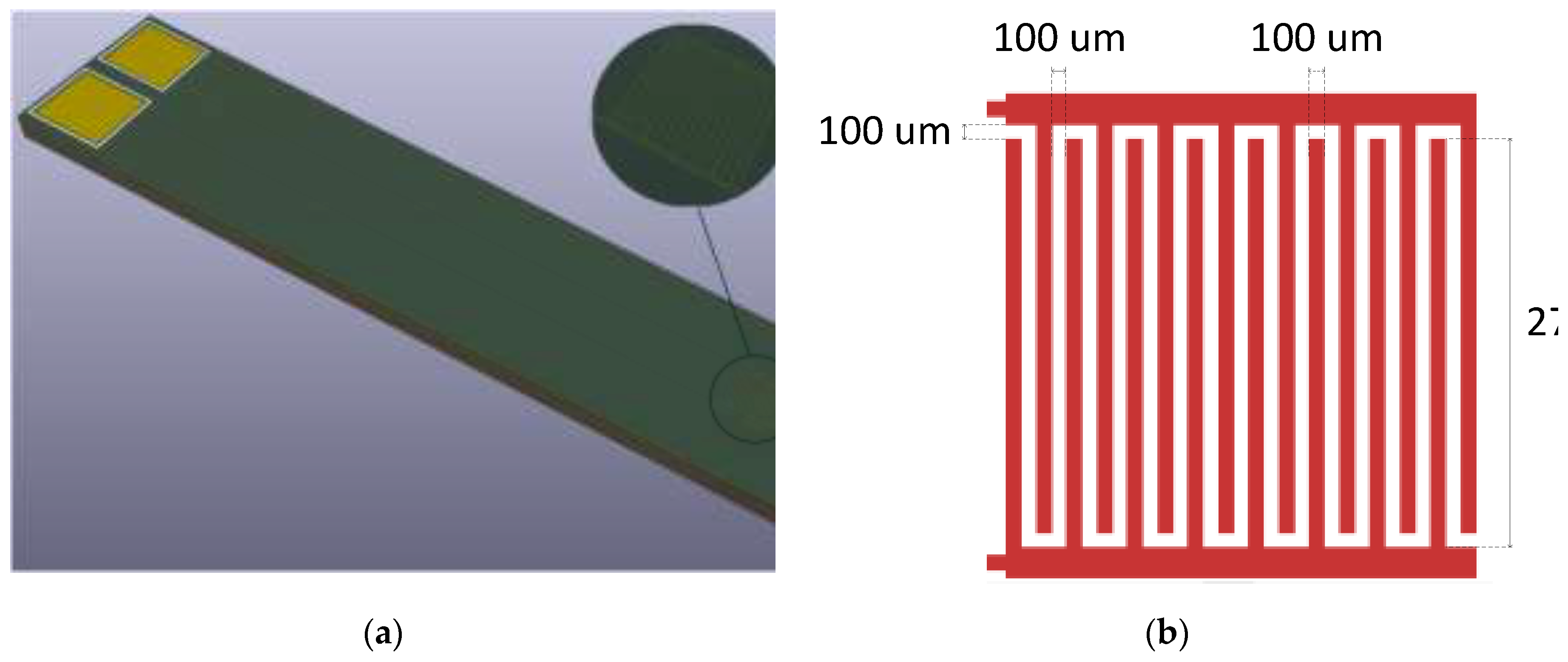
Figure 2.
ATR-FTIR spectra of epoxy resin samples. The blue spectrum corresponds to a PCB coated with epoxy resin, while the red spectrum represents the epoxy resin after 24 hours treatment with 3-MPA at a concentration of 1000 mM.
Figure 2.
ATR-FTIR spectra of epoxy resin samples. The blue spectrum corresponds to a PCB coated with epoxy resin, while the red spectrum represents the epoxy resin after 24 hours treatment with 3-MPA at a concentration of 1000 mM.
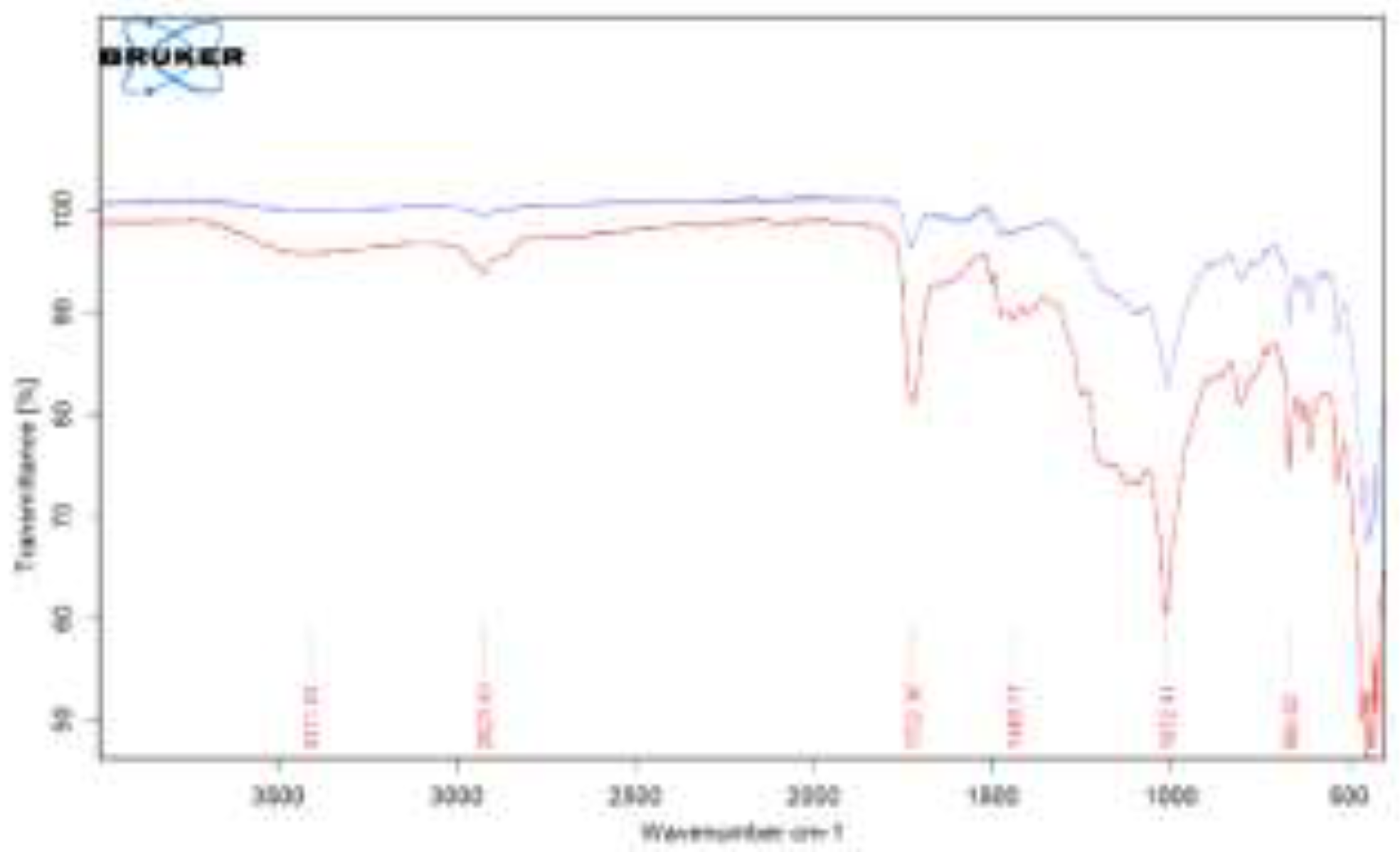
Figure 3.
Variation in the intensity of the ATR band at 1725 cm⁻¹ on the PCB surface as a function of the 3-MPA concentration applied.
Figure 3.
Variation in the intensity of the ATR band at 1725 cm⁻¹ on the PCB surface as a function of the 3-MPA concentration applied.
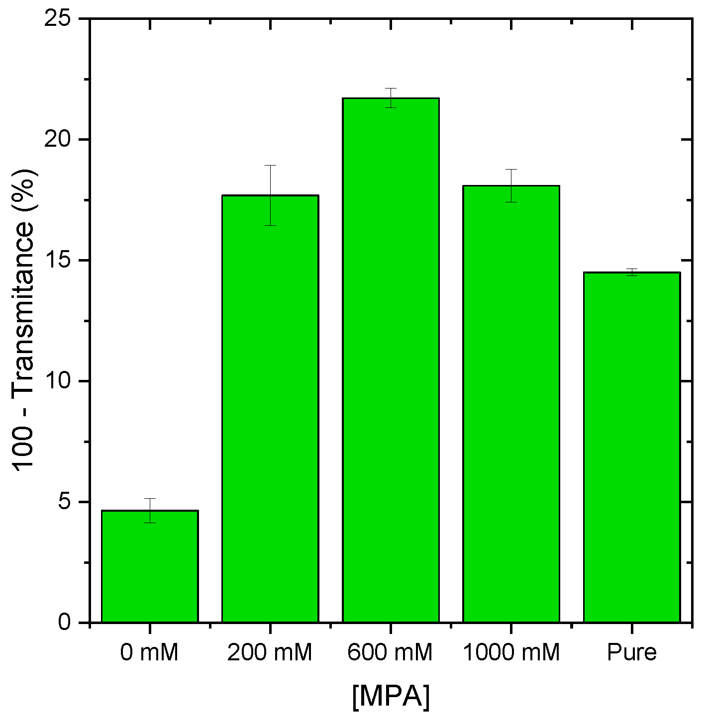
Figure 4.
ATR-FTIR spectra of epoxy resin samples. The blue spectrum corresponds to a PCB coated with epoxy resin after 24 hours treatment with 3-MPA, while the red spectrum corresponds to a PCB after covalent immobilization of BSA.
Figure 4.
ATR-FTIR spectra of epoxy resin samples. The blue spectrum corresponds to a PCB coated with epoxy resin after 24 hours treatment with 3-MPA, while the red spectrum corresponds to a PCB after covalent immobilization of BSA.
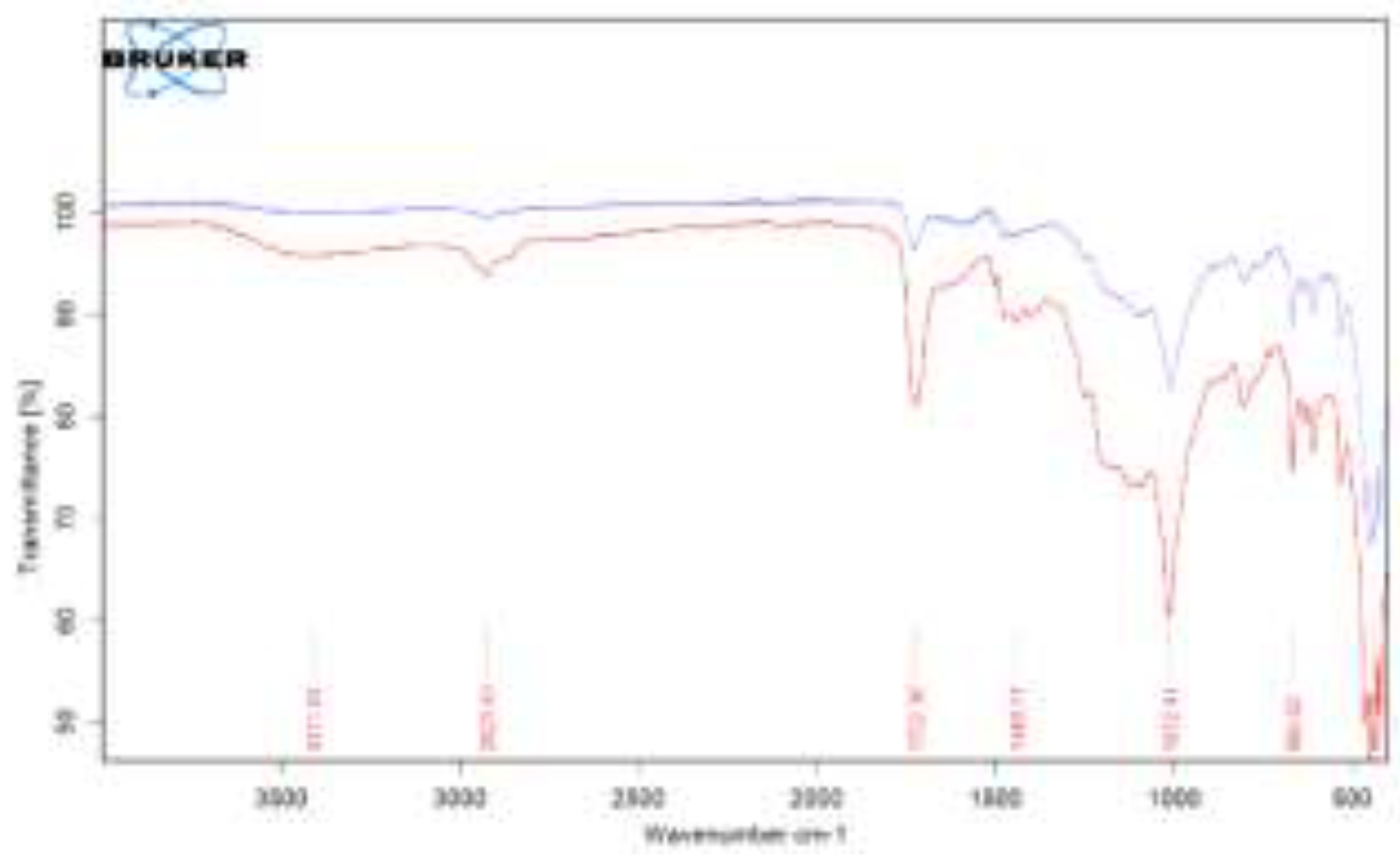
Figure 5.
BCA assay results showing three independent replicates for the functionalized resin.
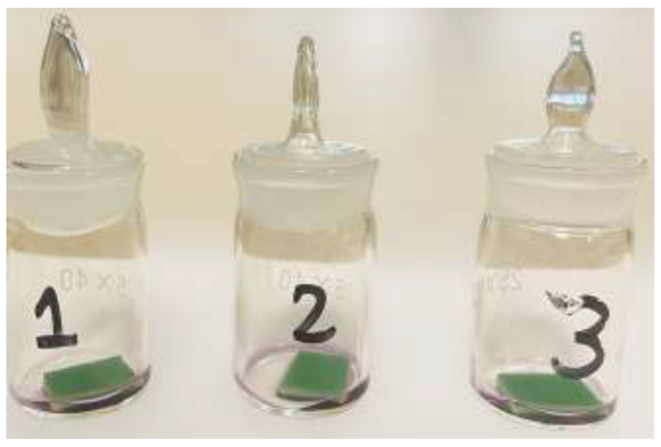
Figure 6.
Impedance spectroscopy plots for sensors 1 (a), 2, (b) and 3 (c). B: non-functionalized sensor; F: functionalized sensor; A: functionalized sensor after analyte recognition.
Figure 6.
Impedance spectroscopy plots for sensors 1 (a), 2, (b) and 3 (c). B: non-functionalized sensor; F: functionalized sensor; A: functionalized sensor after analyte recognition.
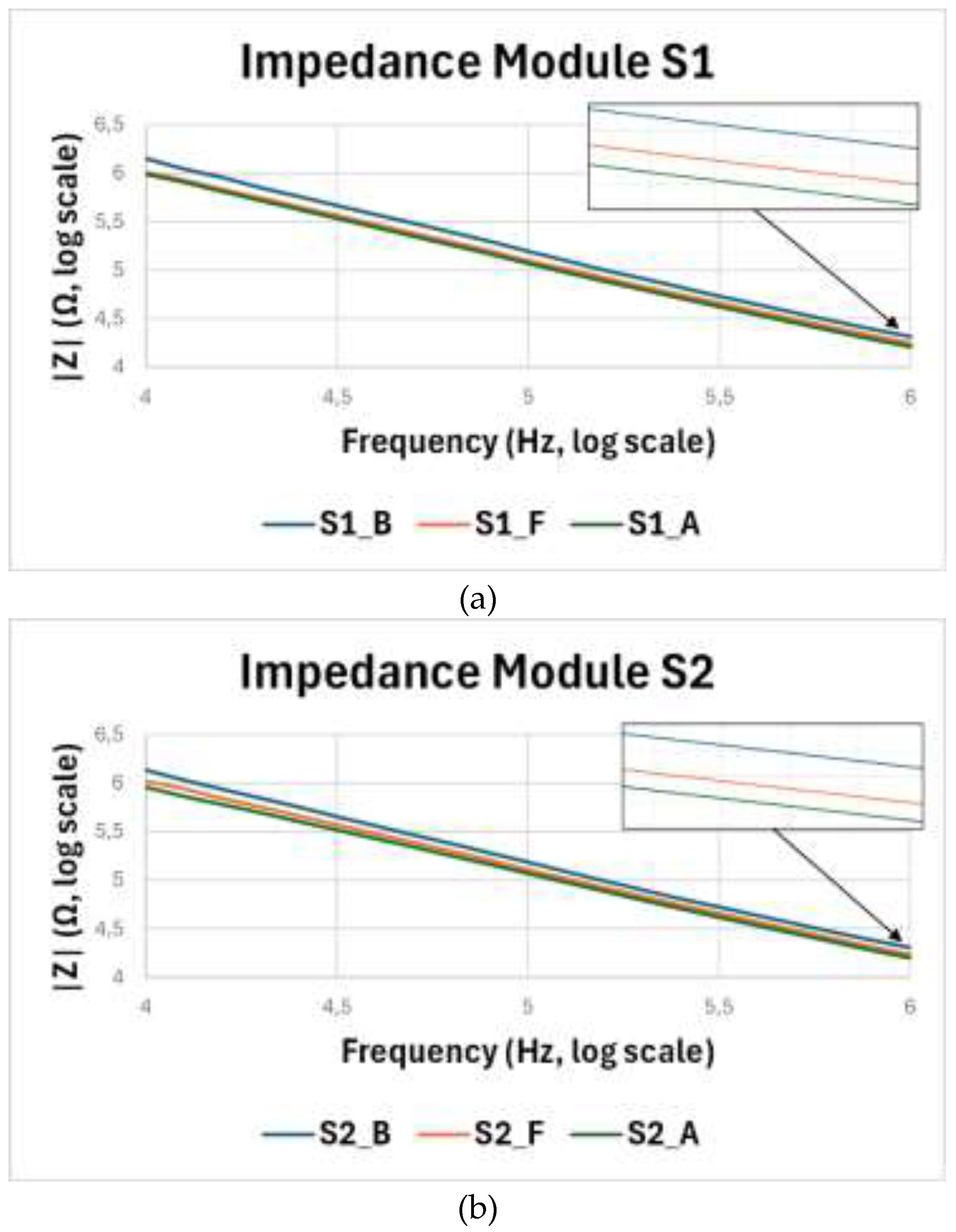
Figure 7.
Variation of the impedance magnitude with respect to the bare state (average and standard deviation).
Figure 7.
Variation of the impedance magnitude with respect to the bare state (average and standard deviation).
Disclaimer/Publisher’s Note: The statements, opinions and data contained in all publications are solely those of the individual author(s) and contributor(s) and not of MDPI and/or the editor(s). MDPI and/or the editor(s) disclaim responsibility for any injury to people or property resulting from any ideas, methods, instructions or products referred to in the content. |
© 2026 by the authors. Licensee MDPI, Basel, Switzerland. This article is an open access article distributed under the terms and conditions of the Creative Commons Attribution (CC BY) license (http://creativecommons.org/licenses/by/4.0/).
Copyright: This open access article is published under a Creative Commons CC BY 4.0 license, which permit the free download, distribution, and reuse, provided that the author and preprint are cited in any reuse.


