Submitted:
28 January 2026
Posted:
06 February 2026
You are already at the latest version
Abstract
To meet the requirements for high-precision acquisition of multi-channel weak current signals in magnetic field tomography diagnostics for the CN-H1 star-simulator, this paper presents a 64-channel microcurrent data acquisition system based on the ZYNQ-7000 SoC. The system employs independent high-gain transimpedance amplification and filtering circuits for front-end conditioning. Utilising FPGA control over four AD4115 analogue-to-digital converters, it achieves parallel high-precision acquisition of 64 signals. Experiments demonstrate that within the ±2 μA input range, the system's equivalent input noise remains below 0.2 nA (RMS). The average effective number of bits (ENOB) per channel reaches 13.28 bits, with high inter-channel consistency (standard deviation of 0.04 bits). This system combines high channel density with outstanding single-channel measurement performance, making it suitable for precision measurement scenarios requiring parallel, high-precision acquisition of minute currents.
Keywords:
CN-H1
; weak signal acquisition
; high-precision measurement
; multi-channel
; ZYNQ
; AD4115
1. Introduction
The magnetic field configuration of a stellarator is independently generated by external coils, and its vacuum magnetic topology can be directly measured through magnetic field mapping under plasma-free conditions [1]. This diagnostic technique is based on the principle of electron cyclotron motion along magnetic field lines and employs electron beam tracing to reconstruct magnetic field distributions by analyzing electron trajectories [2,3]. At the China No. 1 Heliotron (CN-H1) device of the University of South China, an electron beam is directed to strike a rotating grid array. By detecting the spatial distribution of minute current signals and combining them with tomographic inversion, detailed magnetic field structure information can be obtained [4].
This diagnostic method requires high-precision measurement of nA-level microcurrents collected from 64 rotating grid channels. Such signals are characterized by extremely low amplitudes and are highly susceptible to thermal noise, electromagnetic interference, and non-ideal system effects [5,6,7], placing stringent requirements on noise suppression capability and long-term system stability. Moreover, multi-channel parallel acquisition inherently introduces channel crosstalk, power-supply coupling noise, and synchronization timing errors, resulting in a pronounced trade-off between channel density and measurement accuracy. Conventional general-purpose current acquisition schemes struggle to simultaneously satisfy the demands for high resolution [8], multi-channel consistency [9], and system stability [10]. Similar challenges have been reported in the magnetic diagnostics of the HL-2A tokamak, where real-time digital integrators are employed to mitigate errors caused by drift and channel asynchronism [11]. In recent years, significant progress has been made in multi-channel weak-current acquisition systems, with several implementations achieving high-precision and highly consistent synchronous measurements [12,13,14].
To address these challenges, this work develops a 64-channel microcurrent data acquisition system based on the ZYNQ-7000 SoC. Through optimized system architecture and circuit design, the proposed system integrates low-noise transimpedance amplification, highly stable power-supply and clock management, and continuous multi-channel acquisition using multiple Σ–Δ ADCs [15]. While maintaining a high channel density, the system demonstrates excellent single-channel measurement performance. Experimental results indicate that the proposed system exhibits favorable noise characteristics, effective number of bits, and channel-to-channel consistency [16]. The system satisfies the diagnostic requirements for high-precision magnetic field mapping on the CN-H1 device and provides a reliable solution for similar multi-channel weak-current measurement applications.
2. System Analysis
A high-precision multi-channel signal processing and data acquisition system is designed and implemented in this work. The system is built around a self-developed board based on the Xilinx ZYNQ-7000 series SoC. As illustrated in Figure 1, the overall architecture consists of five main components: a signal conditioning circuit, an analog-to-digital (A/D) conversion module, a data buffering module, a timing and logic control unit, and a host-side processing unit. The system is intended for plasma diagnostics and weak-signal measurement applications, aiming to achieve high-precision acquisition and reliable real-time transmission of multi-channel analog signals.
During operation, analog signals generated by external sensors are first amplified and filtered by the signal conditioning circuit to improve the signal-to-noise ratio and suppress out-of-band noise, thereby ensuring the stability and reliability of the signals fed into the A/D converters. Under the control of a global sampling clock (CLK1), the A/D conversion module performs synchronous sampling and quantization of multi-channel signals, and the resulting digital data are transferred to the data buffering module. Driven by an independent clock (CLK2), the buffering module enables high-speed temporary storage and orderly data output, effectively alleviating the rate mismatch between high-speed sampling and back-end data transmission.
The timing and logic control of the system are implemented by the programmable logic (FPGA), which coordinates the timing relationships among sampling, buffering, and data transmission operations to ensure stable system operation and data stream consistency. The processing system (ARM) is responsible for data parsing and communication tasks, and the acquired data are transmitted in real time to the host computer via a high-speed Ethernet interface for further processing and visualization.
3. Hardware and Software Implementation
3.1. Hardware Design
3.1.1. Hardware Design of the Signal Conditioning Module
In electron gun–grid tomographic diagnostics, the signals collected by the grid are present in the form of extremely weak currents, which cannot be directly measured with high accuracy [7]. To satisfy the requirements of subsequent analog-to-digital conversion and digital signal processing in terms of signal amplitude and signal-to-noise ratio, the original current signals must be properly converted, amplified, and filtered prior to data acquisition [8]. Therefore, a dedicated signal conditioning module is designed in this system. By employing an I–V transimpedance amplification circuit, the weak current signals are converted into measurable voltage signals [5,8], while noise suppression and bandwidth limitation are simultaneously achieved.
Figure 2 illustrates the complete schematic of the signal conditioning circuit. The overall transfer function of the conditioning stage can be expressed as Equation (1):
The signal conditioning module mainly consists of an I–V transimpedance amplification stage, a second-order Sallen–Key low-pass filter, and an output buffer stage. Its primary function is to convert weak current signals into voltage signals and to perform filtering and waveform shaping. By selecting operational amplifiers with high input impedance and low noise characteristics, together with an optimized feedback network, a transimpedance gain of 2 × 10⁶ is achieved, corresponding to an overall gain of approximately 126 dB. In addition to providing high gain, the proposed design effectively suppresses noise interference, thereby ensuring stable and reliable signal conditioning for subsequent data acquisition.
3.1.2. Hardware Design of the A/D Conversion Module
After processing by the signal conditioning module, the original weak current signals are converted and amplified into analog voltage signals with amplitudes suitable for analog-to-digital conversion. To ensure that no significant additional errors are introduced during quantization and to satisfy the requirements of high-precision multi-channel acquisition, the data acquisition module must exhibit high resolution, low noise, and good channel-to-channel consistency. Accordingly, a high-precision sigma–delta (Σ–Δ) analog-to-digital converter (ADC) is selected as the core of the data acquisition module [17], enabling reliable quantization of multi-channel weak current signals.
The data acquisition module is implemented using four 24-bit Σ–Δ ADC chips (AD4115) [18], and is specifically designed to support the parallel acquisition of 64 microcurrent channels. The AD4115 provides a configurable sampling rate of up to 125 kSPS, and in multi-channel scanning mode, the effective sampling rate per channel can reach 24.8 kSPS. This configuration achieves a favorable balance between sampling speed and quantization accuracy. Considering that the spectral content of microcurrent signals in plasma diagnostics is predominantly concentrated in the low-frequency range and is highly sensitive to noise, the proposed system fully exploits the excellent noise-shaping and interference suppression characteristics of the Σ–Δ architecture at low frequencies, thereby providing a solid hardware foundation for high-fidelity weak-signal acquisition.
The system controller is based on a Xilinx ZYNQ-7000 SoC (XC7Z045), which enables efficient cooperation between data acquisition and processing tasks through its heterogeneous processing system (PS) and programmable logic (PL) architecture [19]. Specifically, the PL side (FPGA) communicates with the four AD4115 devices via the SPI bus and is responsible for time-critical sampling control, channel switching management, and preliminary data buffering. In contrast, the PS side (ARM) handles system configuration, data packetization, and high-speed data transmission to the host computer. This task partitioning effectively reduces processor workload and enhances real-time performance and system stability under multi-channel, high-sampling-rate conditions [20]. The ADC interface circuitry is illustrated in Figure 3, where the conditioned analog voltage signals are connected to the ADC through Vin0–Vin15, enabling synchronous quantization of multi-channel signals and subsequent high-speed transmission to the host computer for further processing and analysis.
3.2. System Software Design
3.2.1. System Workflow
The system software workflow follows the main sequence of acquisition–buffering–transmission. By leveraging the collaborative architecture of the processing system (PS) and programmable logic (PL) in the ZYNQ-7000 platform [19], the proposed system achieves high-precision multi-channel data acquisition and reliable data transmission. The overall workflow is illustrated in Figure 4.
After system power-up, the power management module supplies multiple independent and low-noise regulated voltages to each functional unit, ensuring long-term stable operation. On the PL side, the master FPGA first initializes the SPI interfaces and configures the operating modes of the ADCs (AD4115). A unified sampling timing sequence is then generated to drive the four ADC devices, each of which performs high-precision sampling and analog-to-digital conversion for 16 corresponding input channels.
Upon completion of each conversion, the 24-bit output data from the ADCs are written in real time into FIFO buffers implemented in the FPGA via the SPI interface. To mitigate the rate mismatch between high-speed sampling and subsequent data processing, the FPGA transfers the buffered data in batches to the PS-side DDR3 memory through the AXI bus, thereby forming continuous data blocks [21].
During experimental operation or when predefined storage conditions are met, the embedded Linux system running on the ARM Cortex-A9 core initiates the data transmission task. Using the TCP/IP protocol stack, the system reliably transfers the temporarily stored data in DDR3 memory to the host computer via a Gigabit Ethernet interface (RJ45). The host-side software is responsible for data reception, channel parsing, real-time waveform visualization, and storage of the raw data in TXT format for subsequent offline analysis and performance evaluation.
This workflow establishes a complete closed loop encompassing independent multi-channel acquisition, real-time buffering, remote data transmission, and visualization, thereby ensuring data integrity and real-time performance in high-precision multi-channel acquisition scenarios.
3.2.2. ADC Driver and Configuration Logic
The AD4115 is configured and read out via an SPI interface, with its timing fully controlled by FPGA logic. Figure 5 illustrates the communication timing of the ADC operating in continuous conversion mode.
During the configuration phase, the FPGA asserts the chip-select signal (CS) low and sequentially writes configuration parameters, including channel selection, sampling rate, and digital filter mode, into the internal registers of the AD4115 through the SPI data input line (DIN). Upon completion of the configuration process, the ADC enters continuous conversion mode.
During the data acquisition phase, at the end of each conversion cycle, the DOUT/RDY pin of the AD4115 outputs a low-level pulse to indicate that new conversion data are available. Once this data-ready signal is detected, the FPGA immediately initiates an SPI read operation. With the chip-select signal (CS) asserted and a serial clock (SCLK) provided, the 24-bit conversion result is shifted out sequentially through the DOUT pin and captured by the FPGA.
3.2.3. FIFO Buffer Design
In a data acquisition system, the processing rates of the A/D converters, FPGA, and display or host modules are inherently different. Direct data transfer without buffering may therefore lead to data loss, glitches, or repeated reads. To address this issue, a FIFO buffering mechanism is introduced into the system design. As a first-in–first-out storage structure implemented using internal FPGA register resources, the FIFO effectively performs data buffering and scheduling functions.
As shown in Figure 6, once the A/D converter completes an analog-to-digital conversion, the resulting digital data are first written into the FIFO buffer. Subsequently, if the FPGA detects a read request from the display or host module, the FIFO outputs the buffered data sequentially for further processing or visualization. If no read request is detected, the data remain stored in the FIFO until the next read operation. This buffering strategy not only enables effective rate matching between different system modules but also ensures stable system operation and data integrity, thereby providing reliable support for high-reliability data acquisition and processing.
3.3. Data Processing Method
In the proposed system, weak current signals from each channel are sampled using a direct ADC data acquisition approach, and the sampling results are stored in text format. The acquired data are saved as unsigned integer values, with each sample occupying 4 bytes to represent the quantized voltage code corresponding to each channel. This code reflects the quantization result of the ADC for the input voltage signal, and the relationship between the digital code and the actual voltage value can be expressed by Equation (2), where Code denotes the stored voltage code in the sampled data.
After the voltage value is obtained, the corresponding current value, expressed in amperes (A), can be further calculated according to Equation (3) by incorporating the transimpedance gain of the front-end signal conditioning circuit. This conversion process establishes a mapping from the raw ADC output codes to the actual physical quantity, thereby providing a computational basis for the quantitative analysis of weak current signals.
In this system, each acquisition channel records 20,000 sampling points, and a total of 64 channels are implemented, resulting in an overall data volume of approximately 5000 kB per acquisition. With a per-channel sampling rate of 20 kSPS, the acquisition duration for a single measurement is approximately 1 s, corresponding to a data transmission rate of about 5 MB/s. This transmission rate falls within the bandwidth capability of the high-speed communication link designed for the system, enabling stable and real-time data upload. The described data acquisition and processing method provides a reliable data foundation for subsequent waveform analysis, multi-channel consistency evaluation, and system performance verification.
4. Experimental Results
4.1. System Test Setup
The experimental platform consists of two regulated power supplies, a waveform generator, a voltage-to-current conversion board with a scaling factor of 1/2490k, the proposed data acquisition system, and a host computer (PC). The waveform generator is used to provide excitation signals required for testing, while the voltage-to-current conversion board emulates the characteristics of weak current signals generated by the detector.
The FPGA-based data acquisition system is responsible for high-precision multi-channel signal sampling and data buffering. The host computer performs data reception, storage, real-time visualization, and subsequent offline analysis. The overall configuration of the experimental platform is illustrated in Figure 7.
4.2. Accuracy and Linearity Verification
4.2.1. Time-Domain Response under Sinusoidal Excitation
To evaluate the accuracy and linearity of the proposed data acquisition system, a sinusoidal excitation test was performed. A 1 V, 100 Hz sinusoidal voltage generated by a signal generator was applied to a voltage-to-current conversion circuit with a scaling factor of 1/2490k, yielding an input current of approximately 400 nA at the front-end signal conditioning stage.
Figure 8 shows the time-domain waveform of the conditioned output signal acquired at a sampling rate of 20 kHz under bipolar input mode, together with the corresponding sinusoidal fitting result. The measured waveform closely follows the fitted sinusoid in terms of amplitude, phase, and periodicity, with no observable waveform clipping or distortion. The output signal exhibits good symmetry with respect to the zero level, with a measured peak-to-peak voltage of approximately 727 mV and a single-sided peak amplitude of about ±0.363 V. Based on the nominal transimpedance gain of the conditioning circuit, the corresponding theoretical input current is 4.02 × 10⁻⁷ A, whereas the peak current extracted from the measured data is approximately 3.69 × 10⁻⁷ A, resulting in an absolute deviation of about 3.2 × 10⁻⁸ A. This deviation remains within an acceptable range for nanoampere-level measurements and indicates a stable and approximately linear response of the acquisition chain under low-frequency sinusoidal excitation.
To further assess the spectral fidelity of the acquisition system, a fast Fourier transform (FFT) was applied to the acquired data, as shown in Figure 9. Under a sinusoidal excitation of approximately 775.4 Hz, the fundamental frequency component is clearly identifiable, while low-amplitude third- and fifth-order harmonic components are also observable. These harmonics are primarily attributed to the non-ideal characteristics of the signal source and the analog front-end circuitry. Quantitative analysis yields a total harmonic distortion (THD) of −88.76 dB and a signal-to-noise ratio (SNR) of 82.55 dB, indicating that the harmonic and noise components are effectively suppressed relative to the fundamental signal. Notably, the observed higher-order harmonics are located outside the effective operating bandwidth of the system and therefore have a negligible impact on the acquisition of target weak signals.
To examine measurement consistency in a multi-channel configuration, five representative channels (CH1, CH8, CH16, CH32, and CH64) distributed across the full channel range were selected and evaluated under identical theoretical input current conditions. The comparison between theoretical and measured peak-to-peak currents is summarized in Table 1.
As shown in Table 1, the relative error between the measured and theoretical peak-to-peak current values for all tested channels is approximately 0.8%. This systematic deviation is mainly attributed to parasitic impedances, leakage currents, and loading effects introduced by the extended analog signal path and multi-stage signal conditioning, which slightly reduce the effective transimpedance gain compared with its ideal value. Importantly, the dispersion of the relative error among different channels remains below 0.02%, demonstrating a high degree of channel-to-channel uniformity. No monotonic trend or channel-index-dependent error is observed, indicating that the proposed system maintains stable and consistent measurement performance across all channels.
4.3. Multi-Channel Consistency and Stability
To evaluate the channel-to-channel consistency and stability of the proposed multi-channel data acquisition system under weak signal measurement conditions, a statistical analysis was performed on the peak-to-peak values of the acquired signals from all 64 channels. The corresponding results are presented in Figure 10.
Let Vpp,i denote the peak-to-peak current measured for the i-th channel. The mean value μ(Vpp) and standard deviation σ(Vpp) across all 64 channels are given by
μ(Vpp) = 3.695 × 10⁻⁷ A
while the corresponding standard deviation is
σ(Vpp) = 2.683 × 10⁻¹⁰ A
Based on these results, the relative dispersion of the peak-to-peak current is approximately 0.07%, indicating that the peak-to-peak values across different channels are highly concentrated and that the channel-to-channel variation is minimal.
4.4. Noise Performance Evaluation
Figure 11 illustrates the measured noise current spectral density of the proposed system under zero-input conditions. As shown, within the frequency range from 10 Hz to 10 kHz, the noise amplitude spectral density remains on the order of 10⁻¹² A/√Hz, indicating an approximately white-noise-dominated behavior over the effective operating bandwidth. In the low-frequency region (1–10 Hz), a slight increase in noise level is observed, which reflects the presence of typical 1/f noise. However, the magnitude of this low-frequency noise remains well controlled, and no obvious low-frequency instability is detected.
To further assess channel-to-channel noise consistency, the median noise spectrum together with the 10th–90th percentile envelope across all channels is presented. The narrow percentile band maintained over the entire frequency range demonstrates good uniformity of noise performance among different channels. In addition, several narrowband interference components appear around 500 Hz and at higher frequencies. These spectral components are mainly attributed to power supply ripple or coupling from digital circuits and have a limited impact on the noise level within the target low-frequency measurement bandwidth of the system.
4.5. Effective Number of Bits (ENOB) Analysis
Under identical test conditions, the quantization performance of the proposed multi-channel microcurrent acquisition system was evaluated by comparing the effective number of bits (ENOB) across all 64 channels. The ENOB is calculated according to Equation (4):
where SNR denotes the signal-to-noise ratio obtained from frequency-domain analysis.
In the experiments, a sinusoidal excitation signal with fixed amplitude and frequency was applied to the system. After the system reached a stable operating state, the output data of each channel were analyzed in the frequency domain using FFT. The corresponding ENOB values were then derived based on Equation (4). This approach enables a consistent and quantitative assessment of the effective resolution and channel-to-channel uniformity of the proposed acquisition system.
The experimental results indicate that the ENOB values across all channels are highly concentrated. The average ENOB is 13.28 bits, with a minimum value of 13.21 bits and a maximum value of 13.36 bits. The corresponding standard deviation is 0.04 bits, demonstrating good channel-to-channel consistency without any noticeably degraded channels. These results verify that the proposed system provides stable and reliable high-precision quantization performance under ideal sinusoidal excitation conditions.
Figure 12.
Distribution of ENOB across all channels.
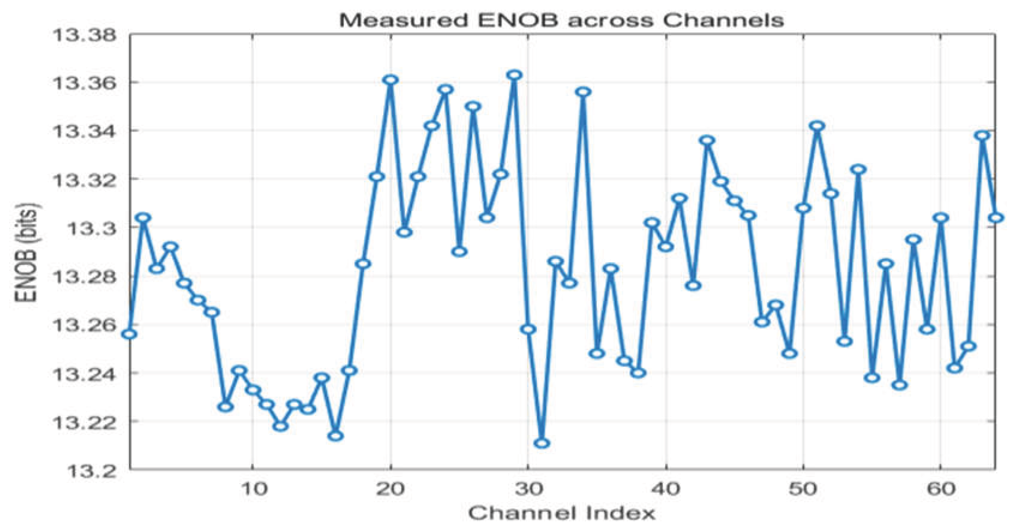
By combining the system input range with the measured ENOB results, the equivalent quantization current step of the worst-performing channel is estimated to be approximately 0.44 nA. Accordingly, the equivalent RMS noise current is better than 0.2 nA. This performance level is sufficient to meet the resolution requirements for precise measurement of nanoampere-level weak current signals.
5. Conclusions
In this work, a 64-channel weak-current data acquisition system based on the ZYNQ-7000 SoC was developed and experimentally validated. By integrating a high-gain, low-noise signal conditioning circuit with multiple Σ–Δ ADCs, the proposed system enables parallel, high-precision acquisition of nanoampere-level current signals across a large number of channels. Experimental evaluations demonstrate that, under zero-input conditions, the system achieves a noise current spectral density on the order of 10⁻¹² A/√Hz. Moreover, the average effective number of bits (ENOB) across all 64 channels reaches 13.28 bits, with a small inter-channel dispersion, indicating good channel-to-channel consistency and stable quantization performance.
These results confirm that the proposed architecture provides a reliable solution for high-precision multi-channel weak-current acquisition. Owing to its combination of low noise, high resolution, and consistent multi-channel performance, the system is well suited for stellarator magnetic field diagnostics and other applications requiring accurate measurement of nanoampere-level current signals.
Funding
This research was funded by the National Natural Science Foundation of China, grant number 12505255.
Institutional Review Board Statement
Not applicable.
Informed Consent Statement
Not applicable.
Data Availability Statement
Data are contained within the article.
Acknowledgments
The authors would like to thank all contributors involved in this study.
Conflicts of Interest
The authors declare no conflict of interest.
References
- Jaenicke, R.; Ascasibar, E.; Grigull, P.; Lakicevic, I.; Weller, A.; Zippe, M.; Hailer, H.; Schworer, K. Detailed investigation of the vacuum magnetic surfaces on the W7-AS stellarator. Nuclear Fusion 1993, 33, 687–704. [Google Scholar] [CrossRef]
- Paschmann, G.; Quinn, J. M.; Torbert, R. B. Sensitive detection of probing electron transport and magnetic field structure in toroidal plasma configuration. Japanese Journal of Applied Physics 1994, 33, 1161–1167. [Google Scholar] [CrossRef]
- Paschmann, G.; Quinn, J. M.; Torbert, R. B.; et al. Results of the electron drift instrument on Cluster. Journal of Geophysical Research: Space Physics 2021, 126, 1161–1164. [Google Scholar] [CrossRef]
- Tumlos, R.B. Studies of vacuum magnetic surfaces in H-1 using tomography. Ph.D. Thesis, The Australian National University, Canberra, Australia, 1994. [Google Scholar]
- Lei, S.J.; Wei, Z.Y.; Chen, G.Y. Design of weak current measurement circuit in space particle detector. Journal of Astronautic Metrology and Measurement 2010, 6, 45–50, (in Chinese with English abstract). [Google Scholar]
- Wei, L.Q.; Lei, S.J.; Fang, M.H. An I-V converter in picoampere current measurement. Instrumentation Analysis and Monitoring 2010, 3, 28–31, (in Chinese with English abstract). [Google Scholar]
- Kim, D.; Goldstein, B.; Tang, W.; Sigworth, F. J.; Culurciello, E. Noise analysis and performance comparison of low current measurement systems for biomedical applications. IEEE Transactions on Biomedical Circuits and Systems 2013, 7, 52–62. [Google Scholar] [CrossRef]
- Chen, K.; Chen, M.; Cheng, L.; et al. A 124 dB dynamic range sigma–delta modulator applied to non-invasive EEG acquisition using chopper-modulated input-scaling-down technique. Science China Information Sciences 2022, 65, 140402. [Google Scholar] [CrossRef]
- Stoyka, K.; Femia, N.; Di Capua, G. Power inductors behavioral modeling revisited. IEEE Transactions on Circuits and Systems I 2020, 67, 5636–5649. [Google Scholar] [CrossRef]
- Kumar, D.S.; Gaurav, S.; Garje, K.; Sushma, P.; Sharada, C. 90 dB dynamic range multi-channel data acquisition ASIC for sonar applications. In Proceedings of the 4th International Conference on Range Technology (ICORT), Chandipur, Balasore, India, 2025; pp. 1–6. [Google Scholar] [CrossRef]
- Chen, C.; Fan, W.W.; Pan, Y.H.; et al. A multi-channel real-time digital integrator for magnetic diagnostics in HL-2A tokamak. Nuclear Science and Techniques 2016, 27, 14. [Google Scholar] [CrossRef]
- Xu, Q. Research on multi-channel weak current quasi-synchronous measurement technology based on FPGA. In Proceedings of the 4th International Conference on Electronic Information Engineering and Computer Communication (EIECC), Wuhan, China, 2024; pp. 99–104. [Google Scholar] [CrossRef]
- Chen, X.; Guo, J. Design of a high-speed multi-channel data acquisition system based on FPGA. In Proceedings of the International Conference on Virtual Reality and Intelligent Systems (ICVRIS), Zhangjiajie, China, 2020; pp. 250–252. [Google Scholar] [CrossRef]
- Jia, L. Algorithm design of multi-channel weak signal detection and synchronous acquisition in communication networks. Wireless Personal Communications, 2022. [Google Scholar] [CrossRef]
- Garcia, J.; Rusu, A. High-Order Continuous-Time Incremental Sigma–Delta ADC for Multi-Channel Applications. In Proceedings of the IEEE International Symposium on Circuits and Systems (ISCAS), Rio de Janeiro, Brazil, 2011; pp. 1121–1124. [Google Scholar] [CrossRef]
- Hua, J.; Yang, P.; Yin, X.; Zhou, Y.; Wang, Y. Timing control system design of stellarator based on virtual instrument. Fusion Engineering and Design 2026, 224, 115625. [Google Scholar] [CrossRef]
- Ding, W.; Wu, T.; Liao, C.; Wang, J.; Jiang, Y. A high-resolution ADC model combining pipeline and sigma–delta oversampling architecture. In Proceedings of the IEEE International Conference on Cognitive Informatics and Cognitive Computing (ICCI*CC), Milan, Italy, 2019; pp. 350–355. [Google Scholar] [CrossRef]
- Analog Devices. AD4115: Low Power, Low Noise, 24-Bit Sigma–Delta ADC with ±10 V and 0 V to 10 V Bipolar Inputs, Rev. G ed; Analog Devices: Norwood, MA, USA, 2020; Available online: https://www.analog.com/media/en/technical-documentation/data-sheets/ad4115.pdf (accessed on 2 April 2024).
- Xilinx. Zynq-7000 SoC Data Sheet: Overview (DS190). Xilinx: San Jose, CA, USA, 2023; Available online: https://www.xilinx.com/support/documentation/data_sheets/ds190-Zynq-7000-Overview.pdf (accessed on 2 April 2024).
- Medina-Hernández, S.M.; Carballo, P.P.; Hernández-Fernández, P.; González, S. Low-cost Zynq FPGA SoC-based data acquisition system for applications in the field of astrophysics. In Proceedings of the 3rd International Conference on Electrical, Computer, Communications and Mechatronics Engineering (ICECCME), Tenerife, Canary Islands, Spain, 2023; pp. 1–5. [Google Scholar] [CrossRef]
- Tyagi, H.; Gajjar, N.P.; Bandyopadhyay, M.; Chakraborty, A. Real-time high-speed novel data acquisition system based on ZYNQ. In Intelligent Computing Techniques for Smart Energy Systems; Kalam, A., Niazi, K., Soni, A., Siddiqui, S., Mundra, A., Eds.; Lecture Notes in Electrical Engineering; Springer: Singapore, 2020; Vol. 607, pp. 725–735. [Google Scholar] [CrossRef]
Figure 1.
Overall block diagram of the analog signal data acquisition system.
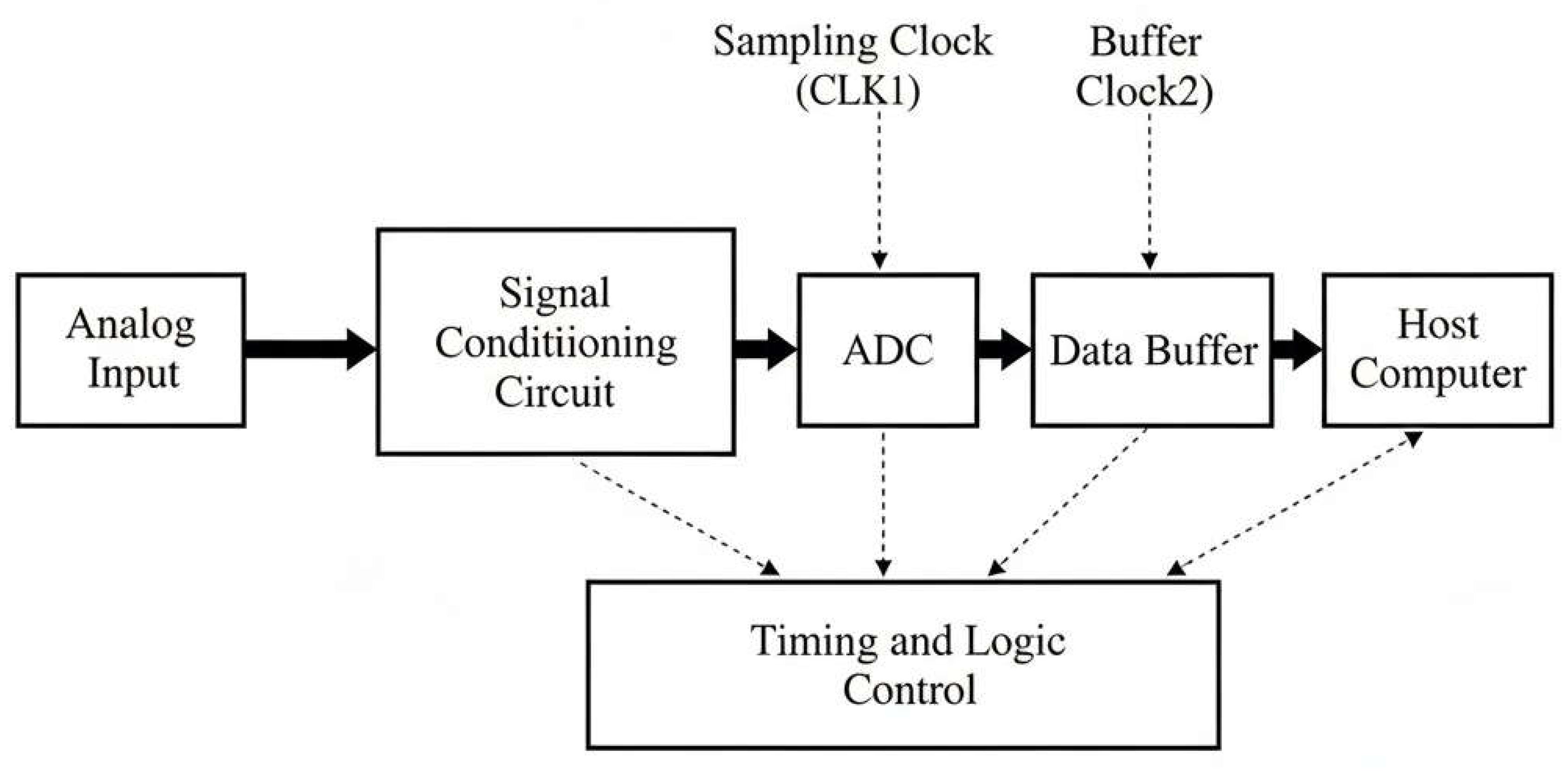
Figure 2.
Simulation circuit of the signal conditioning stage.
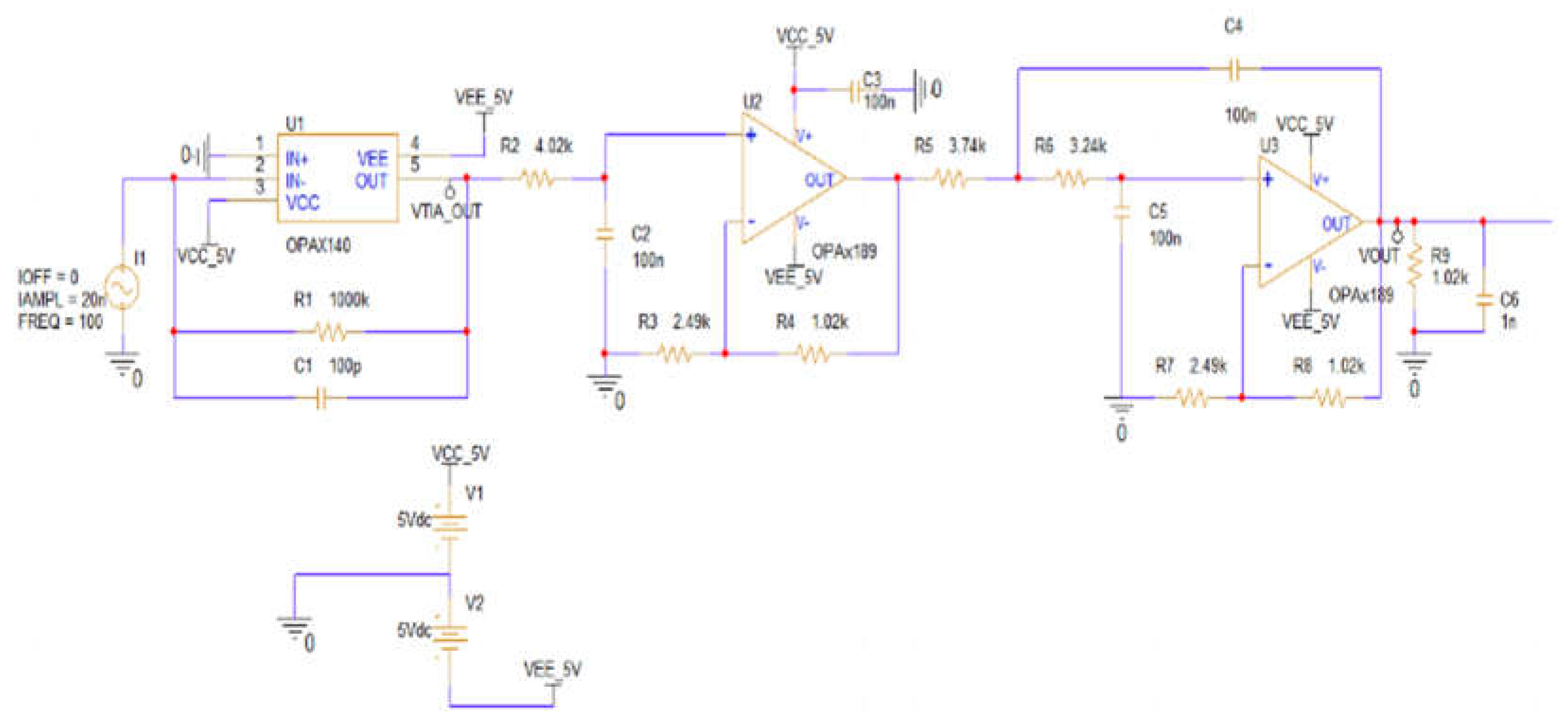
Figure 3.
Interface circuit design of the ADC module.
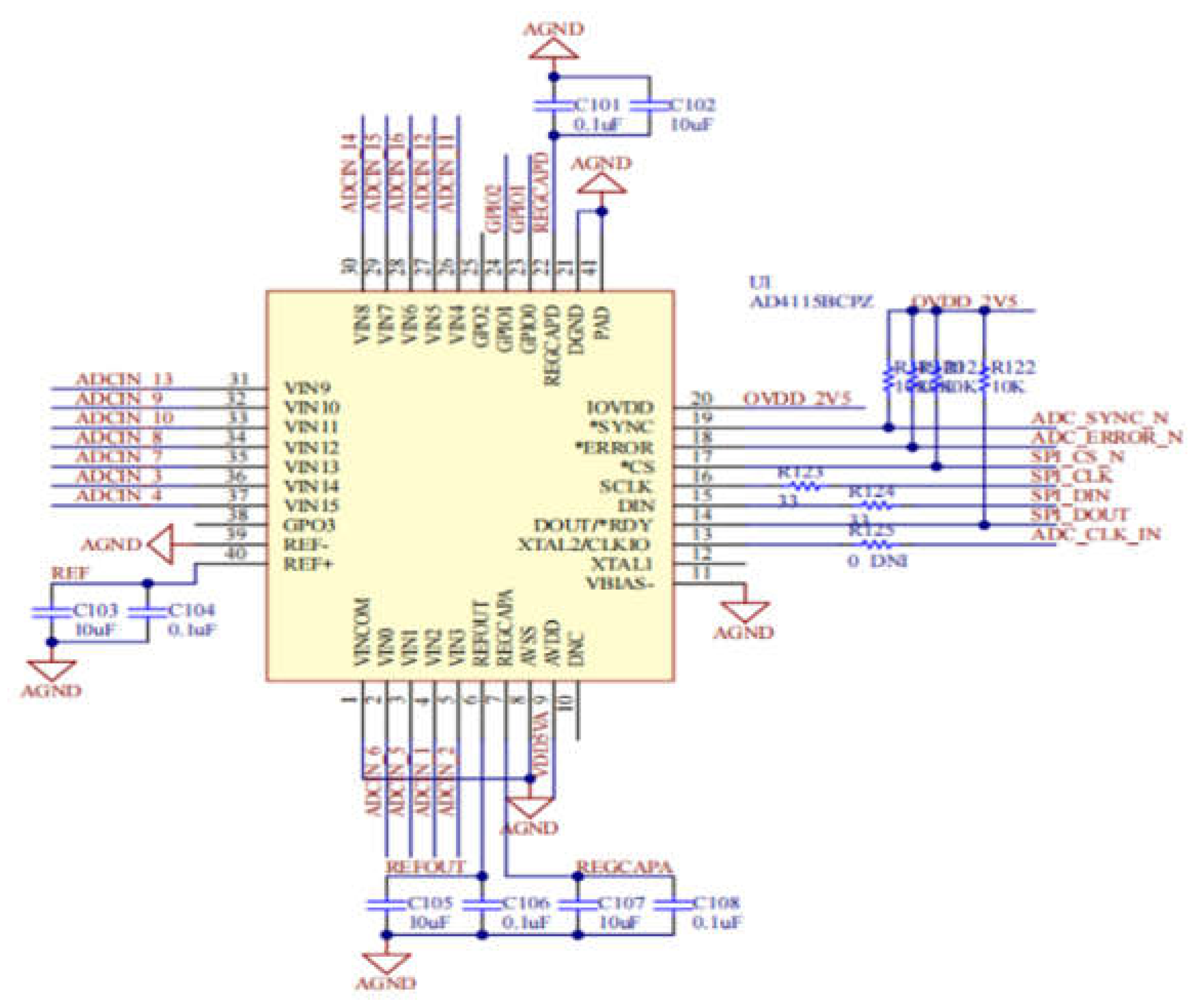
Figure 4.
Software and hardware workflow of the 64-channel ZYNQ-based data acquisition system.
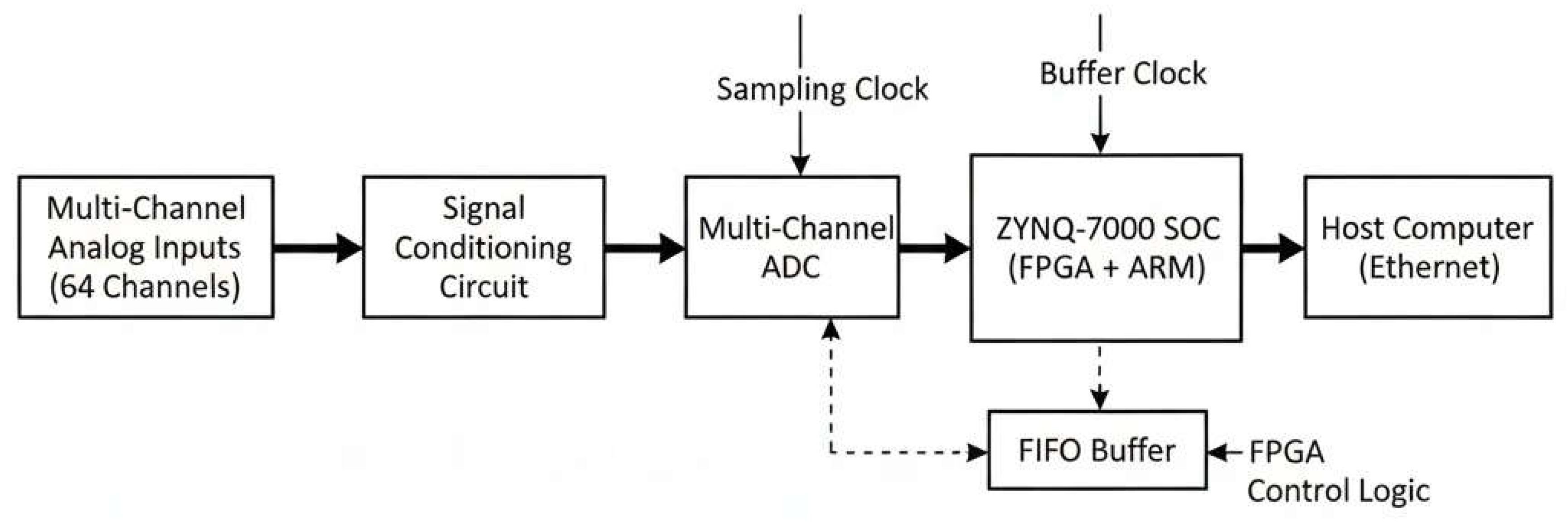
Figure 5.
Timing diagram of the AD4115 in continuous conversion mode.
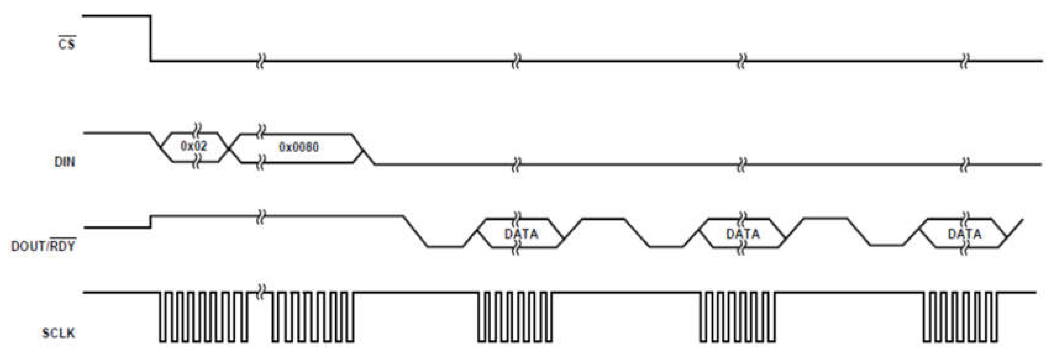
Figure 6.
Flowchart of the FIFO buffer design.
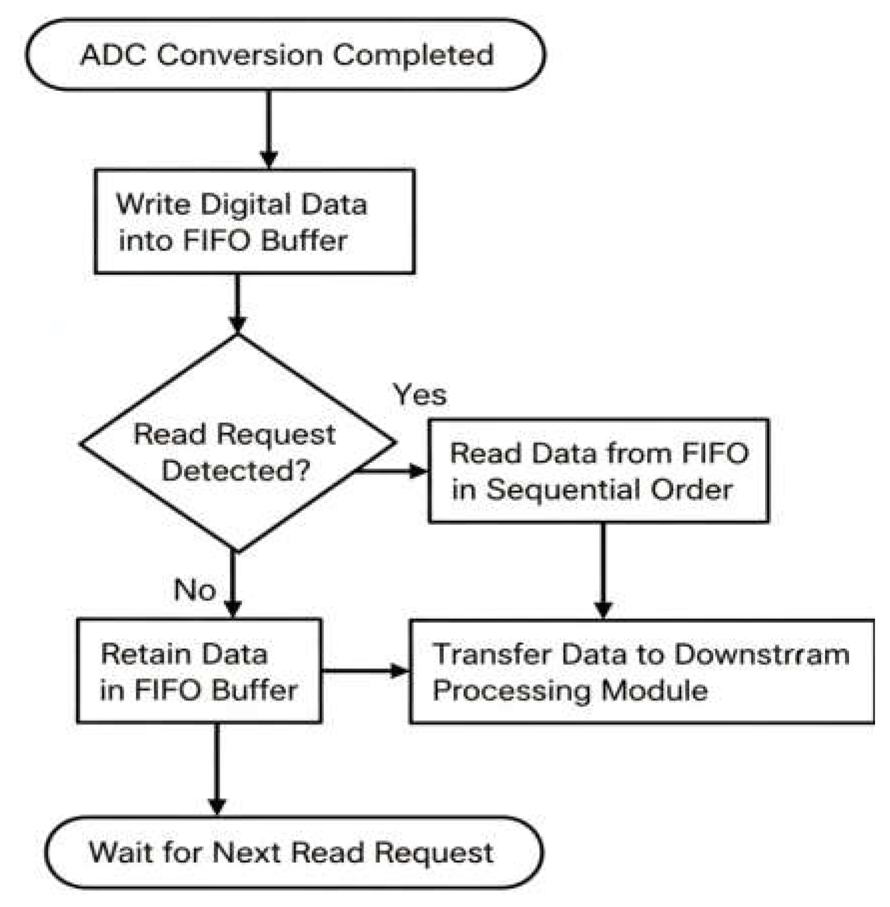
Figure 7.
Architecture of the multi-channel experimental data acquisition platform.
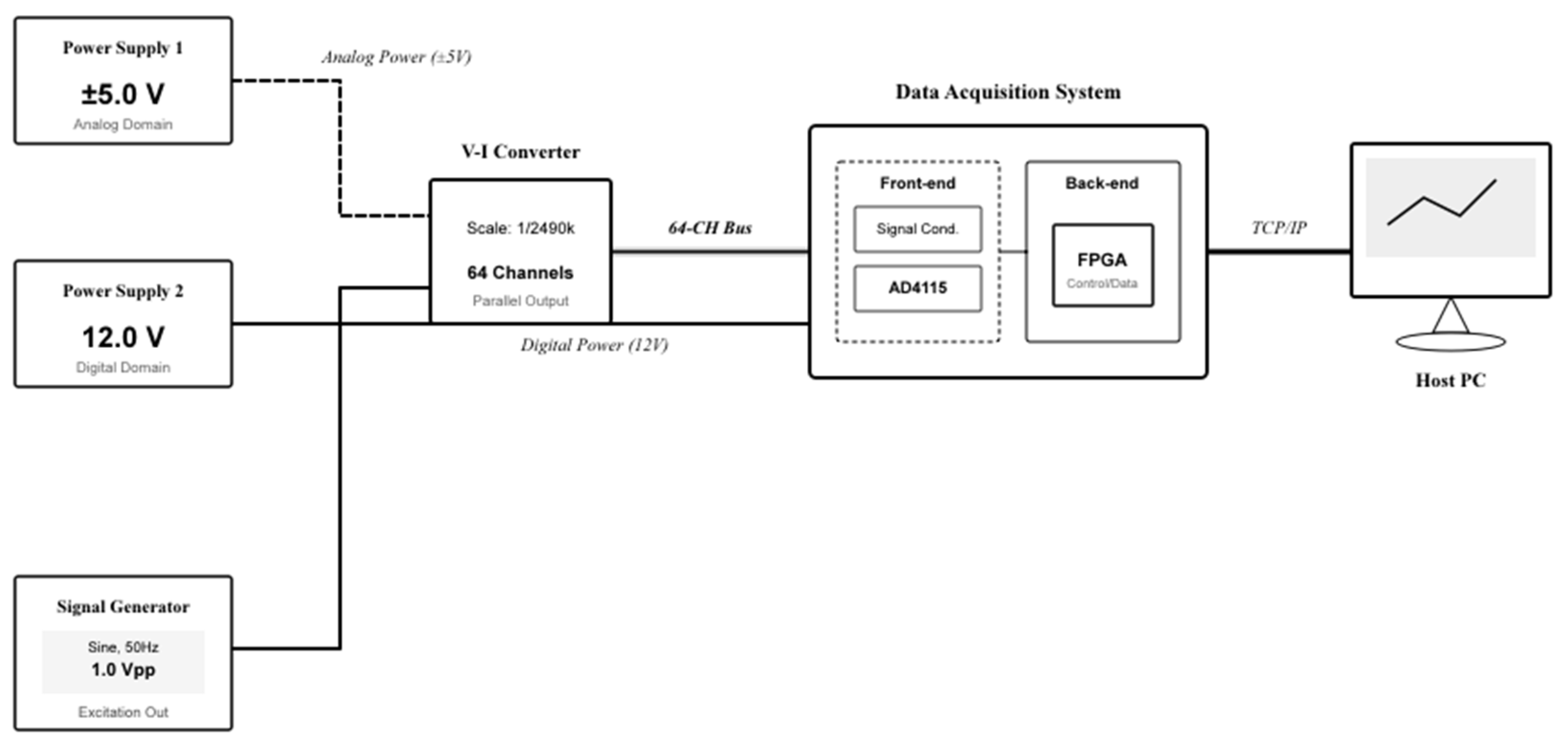
Figure 8.
Time-domain waveform of the conditioned output signal.
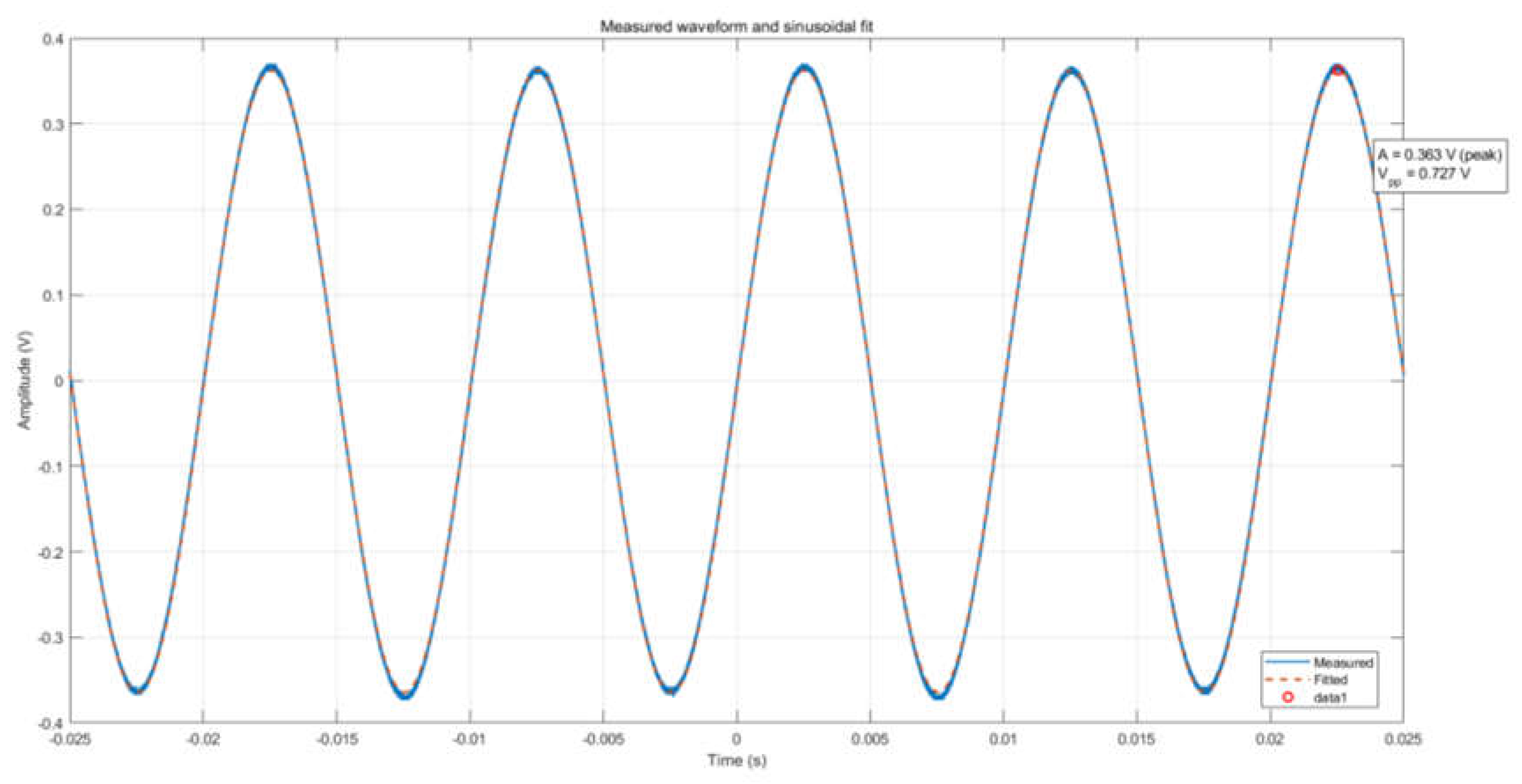
Figure 9.
FFT analysis of the acquired signal.
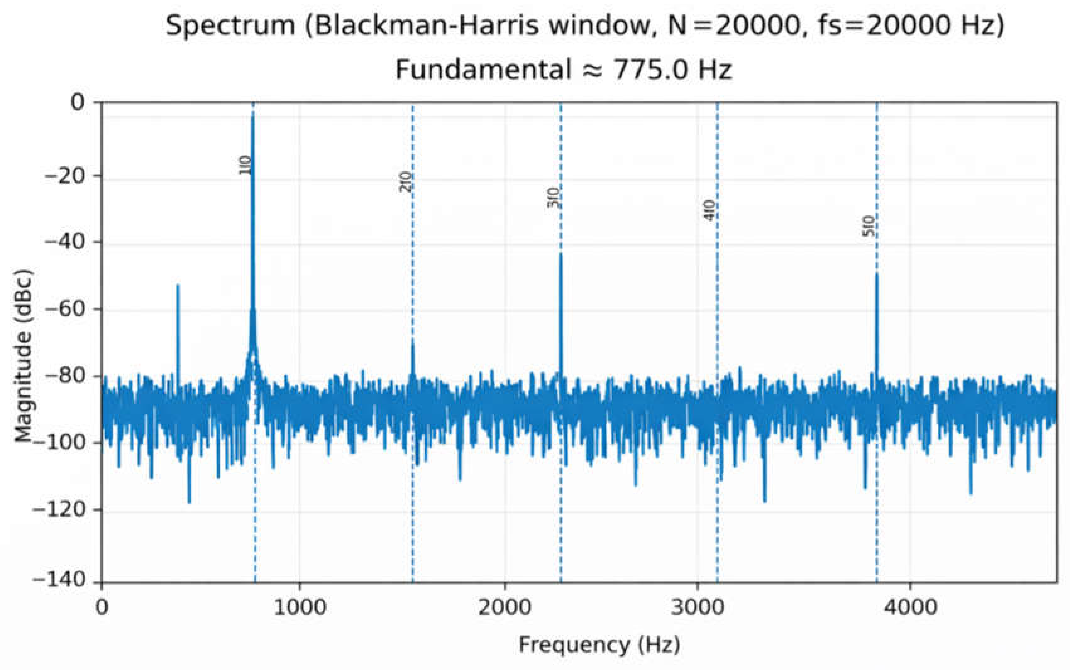
Figure 10.
Statistical distribution of peak-to-peak current values for all 64 channels.
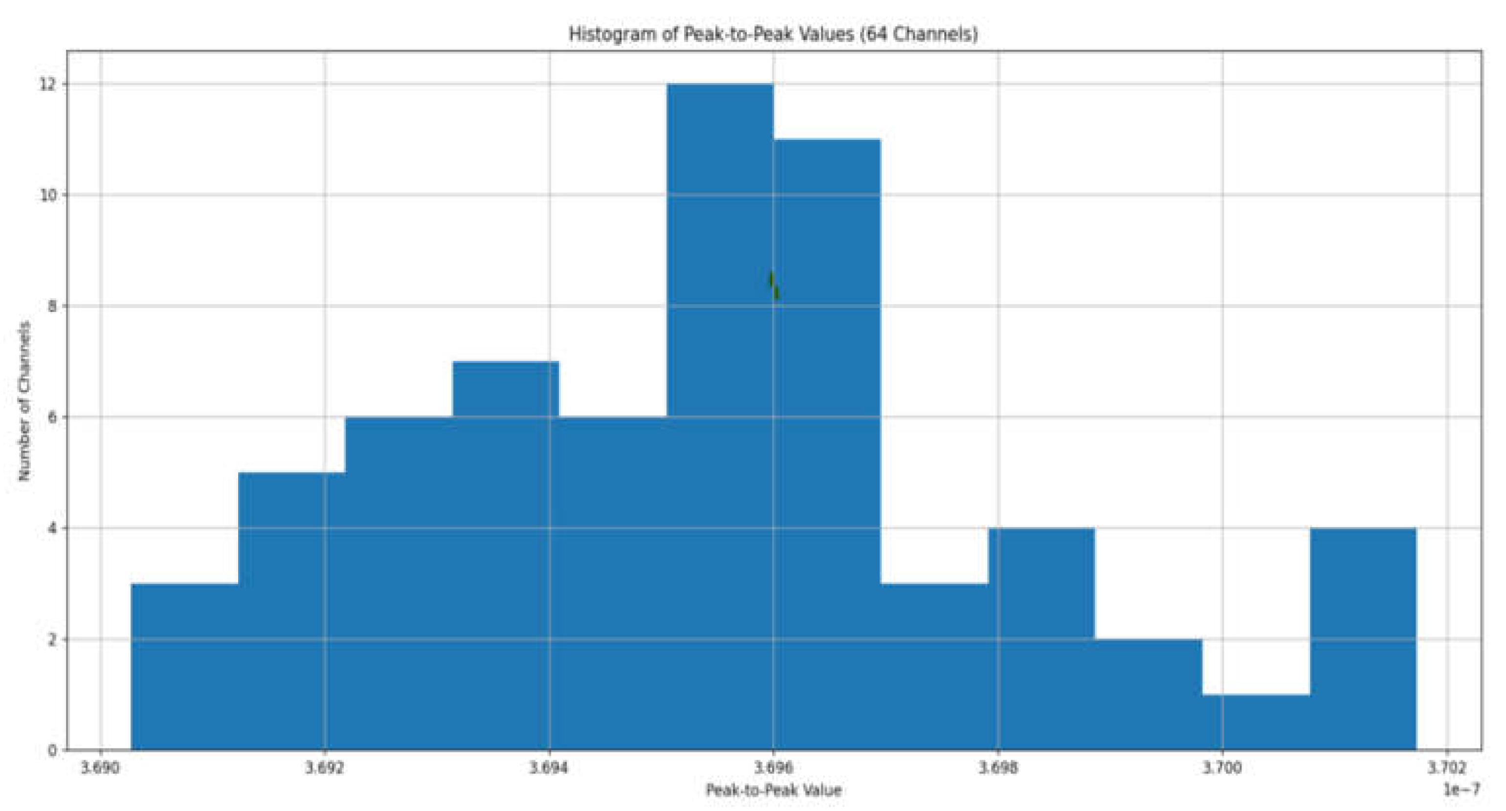
Figure 11.
Noise current spectral density under zero-input conditions.
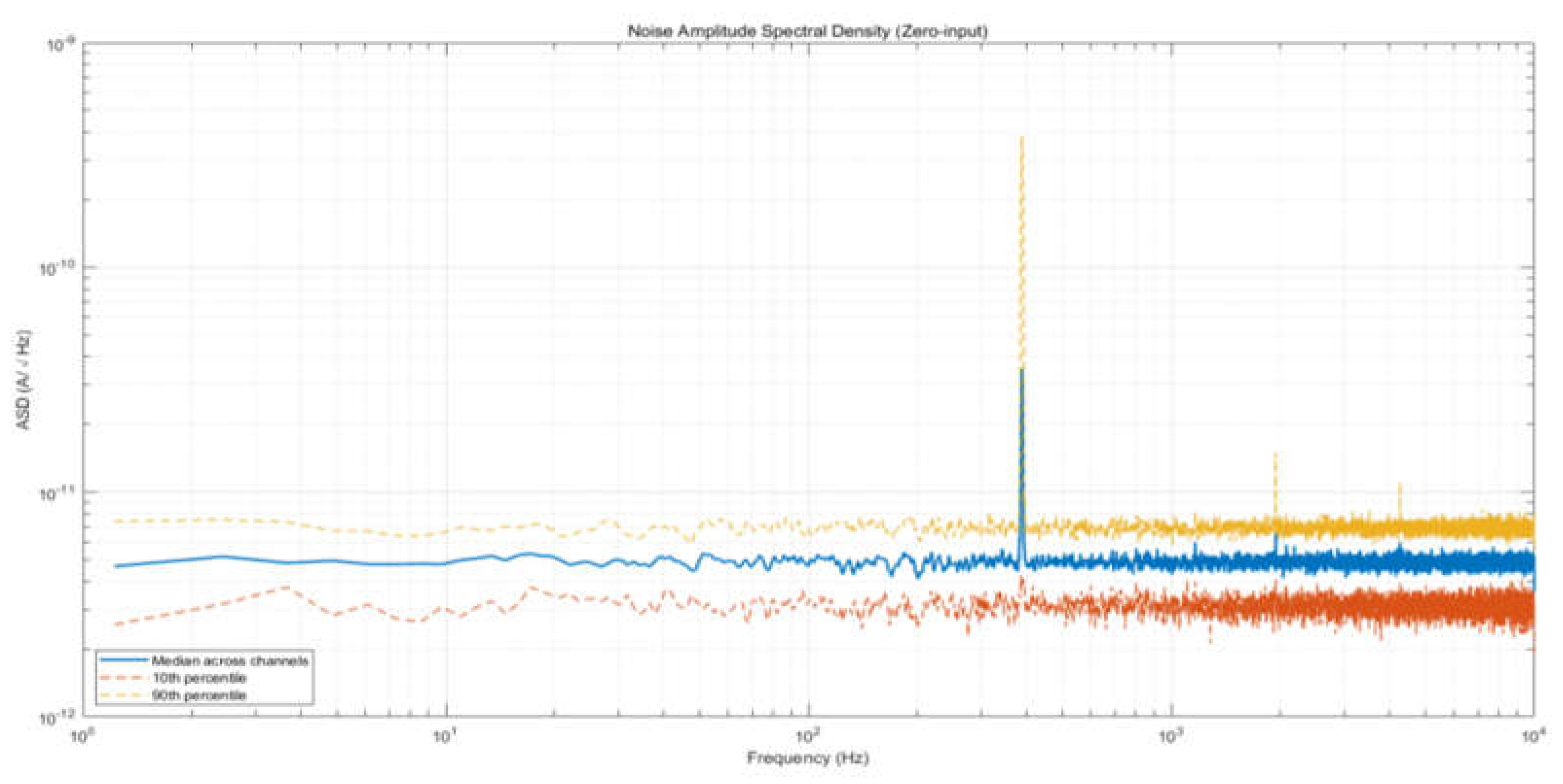

Table 1.
Comparison between theoretical and measured peak-to-peak input currents.
| Channel | Theoretical Peak-to-Peak Current (A) | Measured Peak-to-Peak Current (A) | Absolute Error (A) |
Relative Error (%) |
| CH1 | 4.016064 × 10⁻⁷ | 3.690600 × 10⁻⁷ | 3.25 × 10⁻8 | 0.81% |
| CH8 | 4.016064 × 10⁻⁷ | 3.696635 × 10⁻⁷ | 3.19 × 10⁻8 | 0.79% |
| CH16 | 4.016064 × 10⁻⁷ | 3.696650 × 10⁻⁷ | 3.19 × 10⁻8 | 0.79% |
| CH32 | 4.016064 × 10⁻⁷ | 3.695697 × 10⁻⁷ | 3.20 × 10⁻8 | 0.79% |
| CH64 | 4.016064 × 10⁻⁷ | 3.697917 × 10⁻⁷ | 3.18 × 10⁻8 | 0.80% |
Disclaimer/Publisher’s Note: The statements, opinions and data contained in all publications are solely those of the individual author(s) and contributor(s) and not of MDPI and/or the editor(s). MDPI and/or the editor(s) disclaim responsibility for any injury to people or property resulting from any ideas, methods, instructions or products referred to in the content. |
© 2026 by the authors. Licensee MDPI, Basel, Switzerland. This article is an open access article distributed under the terms and conditions of the Creative Commons Attribution (CC BY) license (http://creativecommons.org/licenses/by/4.0/).
Copyright: This open access article is published under a Creative Commons CC BY 4.0 license, which permit the free download, distribution, and reuse, provided that the author and preprint are cited in any reuse.


