Submitted:
28 January 2026
Posted:
29 January 2026
You are already at the latest version
Abstract
This paper presents the concept of a 2D m × n waveguide-based power combiner (PC) that is scalable with respect to the operating frequency band and number of input ports. To our knowledge, this work reports the first planar (2D) power combiner is reported. The novelty of the approach relies on using H-plane rectangular waveguide T-junctions and low-loss polarization twisters in between vertically stacked T-junctions to facilitate scalability. The work is motivated by the aim to coherently combine the output power of multiple modified uni-travelling carrier (MUTC) Terahertz (THz) waveguide photodiodes (PD) in a 2D array configuration. In the manuscript, the design of a 2×2 planar waveguide power combiner for the WR3 band (220–320 GHz) is reported and it is also shown that this block can be further extended to m × n input ports. Full-wave numerical analysis of the proposed 2×2 power combiner shows a return loss of 11 dB at the output port and an average transmission coefficient of about -6.5 dB, i.e., an overall power combining efficiency of ~90%. Furthermore, to enable 2D photodiode array integration, the manuscript presents a new slot-bow tie antenna integrated MUTC photodiode for radiating the optically generated THz power from each PD vertically into the rectangular waveguide. Reflection loss and insertion loss for the slot bow-tie antenna are shown to be better than 10 dB and 1.4 dB over the full WR3 band, respectively. To prove scalability of the power combiner concept w.r.t. the number of input ports, also a 2×4 power combiner is analyzed. Results reveal a return loss better than 10 dB from 225 to 318 GHz and a transmission coefficient of approximately -9.7 dB at 300 GHz, i.e., a power combining efficiency of ~85%.
Keywords:
Terahertz
; integrated optoelectronics
; WR3-waveguide
; 2D 2×2 WR3-power combiner
; terahertz photodiode (THz-PD) arrays
; slot bow-tie antenna
1. Introduction
The terahertz (THz) spectrum, which ranges from 0.1 to 10 THz, is the space between microwaves and infrared regions, exhibiting distinct electromagnetic properties. Historically, the advancement of THz systems has encountered difficulties; however, recent years have witnessed significant advancements in sources, detectors, and system development [1,2]. Photonic-based sources provide a core technology for generating THz signals. These sources are commonly classified as THz lasers and laser-pumped photonic devices, including photomixers [3,4]. Photomixing, also known as optical heterodyne conversion, is a widely used technique for generating tunable continuous-wave (CW) THz radiation by illuminating an ultrafast photodiode or photoconductive device with two optical lasers whose frequency difference lies in the THz band [5]. Because the beat frequency between the lasers is converted into an electrical current oscillation in a photomixer, the output can provide high spectral purity and low phase noise-qualities especially valuable for high-resolution spectroscopy and coherent THz applications [6]. Current developments focus on enhancing output power, quantum efficiency, and integration with planar antennas or photonic platforms. The performance of chip-scale THz sources, including traditional photoconductive antennas (PCAs) and photodiodes (PDs), diminishes above 300 GHz due to transit time and RC-time limitations, hence restricting the saturation output power of small dies in the THz regime, for example, the maximum RF power obtained from a single THz PD is -3 dBm at 300 GHz due to its RC response time [7,8].
To achieve higher power levels of THz PDs, power combining techniques are commonly employed. THz power combiners can be typically classified according to the combining technique, such as: on-chip, free-space, and based-waveguide power combiners [9,10,11].
The on-chip power combiners integrate multiple THz-PDs on a single planar substrate using planar transmission lines, couplers, or corporate-feed networks, providing scalability and potential for integration. However, these on-chip combiners often suffer from high losses at high frequencies and limited bandwidth due to substrate modes, conductor losses, and impedance mismatches [9]. For instance, an on-chip T-junction was utilized to combine the output power of two THz PD chips at 300 GHz. Although on-chip combiners provide compactness and integration potential, this example underscores practical limitations: the enhancement in combined output power was noted only over a limited portion of the operating bandwidth, scalability to more ports or additional THz PDs is limited, and thermal constraints can further restrict performance. Additionally, the RC time constant of the devices limits high-frequency operation [12].
Free-space and waveguide-based combiners present alternative approaches for enhanced power combining, offering wider bandwidth and reduced loss. Free-space combiners, including beam splitters or quasi-optical grids, facilitate the spatial combination of THz PD outputs; nevertheless, they tend to be bulky and sensitive to precise alignment, hence constraining their use in compact integrated system [10,11,13].
Power combiners based on waveguides in metallic structures can be categorized as E-plane, H-plane, and hybrid junctions. The implementation of these combiners becomes progressively more difficult as the number of input ports increases, owing to the demands of fabrication precision and the accumulation of insertion losses.
Choosing a suitable power combining method necessitates a balance between complexity, integration level, and frequency performance; for example, highly integrated on-chip power combiners, e.g. Wilkinson power combiner, may enhance compactness but are not quite scalable in terms of the number of input ports and also elevate loss and manufacturing challenges. The motivation behind this work is to develop a power combiner for a 2D array of THz photodiodes. Because on-chip power combiners are lossy and do not provide wide operational bandwidths and free-space power combiners would become too bulky and would challenge optical coherency, a waveguide-based power combiner has been developed in this work. In general, waveguide-based power combiners can be differentiated into linear and planar arrangements. A linear waveguide power combiner (WR-PC) provides design simplicity and eases manufacturing by arranging the waveguide inputs along a single linear axis. However, as the number of input sources increases, the uneven distribution of the field leads to reduced combining efficiency and increased insertion losses [11]. For example, the linear eight-port rectangular waveguide power divider presented in [11], fabricated using low-cost CNC technology for heterodyne receiver array applications, exhibits a back-to-back insertion loss of 6.2 dB at 220 GHz and can only be used within a fraction of the full waveguide band. The significant insertion loss and bandwidth limitations illustrate the practical limitations of linear input arrangements in attaining effective power combining for multi-port THz power combiners over wide bandwidths.
To address the limitations of linear input THz waveguide power combiners, including restricted scalability, uneven field distribution, reduced power combining and limited operational bandwidth, we propose a planar scalable 2×2 wavgeuide-based power combiner (WR-PC) (i.e. a combiner with four waveguide input ports and one waveguide output port) designed for operation over the full WR3-band (220-320 GHz). It is shown that, thanks to the incorporation of low-loss polarization twisters, the proposed architecture is scalable with respect to the number of input ports, allowing integration of larger 2D THz-PD arrays. To our knowledge, this work presents the first reported concept of a planar (2D) waveguide based THz power combiner.
This paper is organized as follows. Section 2 delineates the design of a 2×1 waveguide power combiner, which constitutes the fundamental component for the proposed 2D 2×2 array configuration. Section 3 elaborates on this notion within a 2×2 configuration, adressing the comprehensive design and the integration of low-loss polarisation twisters to guarantee mode and polarization alignment for effective power combining as well as for scalability. Section 4 addresses the integration of the power combiner with an arrays of THz photodiodes. This includes the design and analysis of new slot bow-tie antenna integrated aveguide-type MUTC photodiodes for vertical coupling of the optically generated THz signals into a waveguide input port of the power combiner. Finally, Section 5 summarizes the main findings and outlines potential directions for future work.
2. THz 2×1 WR3-Power Combiner
2.1. Design Principle
The 2×1 WR-PC is designed to merge the outputs of two THz photodiodes into a single waveguide output while minimizing reflection and insertion loss. The layout of the developed 2×1 WR3-PC is shown in Figure 1. The WR3-PC features two symmetrical standard WR3-waveguides inputs and one WR3-waveguide output to provide an in-phase interference of the input signals at the output section. This geometry follows the fundamental properties of a lossless passive three-port network T-junction [15].
To clarify the power-combining mechanism, the behaviour of the proposed WR3-PC is analyzed using S-parameter power-wave theory. Let ai and bi denote the incident and outgoing waves at port i, respectively. The output wave at the combining port for Figure 2 (port 1) is expressed as
b1=S12a2+S13a3 ……
Assuming coherent excitation of equal amplitude and phase (a2=a3=a0) at ports 2 and 3, and for an ideal, lossless combiner where ∣S12∣=∣S13∣= 1/ (−3 dB in amplitude), the output wave amplitude becomes
The corresponding output power, proportional to ∣b1∣2, is
Pout∝∣b1∣2=2∣a0∣2 ……
Each input port contributes an incident power of ∣a0∣2, resulting in a total input power Pin=2∣a0∣2 . Under the assumption of ideal matching and lossless operation, the combined output power satisfies Pout= Pin, energy conservation for coherent in-phase excitation.
The rectangular waveguide in this configuration has the standard cross-sectional dimensions of a WR3 waveguide, a×b = 864 × 432 µm2 for supporting only the propagation of the dominant TE10 mode. The junction area, in which the two input signals are combined, is optimized to ensure efficient combining, and the corners of the input waveguides are rounded to minimize the reflection of the EM-waves caused by the waveguide 90° sharp corners. Moreover, a septum element (denoted as Sw and Sl) was adopted [16] within the combining region to reduce the undesired coupling between the input ports and to enhance the power combining efficiency. It is worth noting that a rectangular septum’s sharp corners may produce localized electromagnetic field concentrations, which increase the insertion losses (IL) and reflections. The septum’s filleted edges are intended to mitigate these effects and improve impedance matching.
To achieve impedance matching between input/output and the (w1), thereby minimizing signal reflection, the central waveguide section of width (w1, w0) is carefully optimized. On the other hand, (l1) refer to the path length where its lead the EM signals from the inputs to be merged at the combining region core, which tunes the phases of the input signals to provide a constructive interference at the output and has a value of about λg.
This design facilitates effective combination of the two-input power while preserving symmetry and phase integrity, which are paramount for high-frequency systems. The optimized design parameters for full-band and minimum IL are listed in Table 1, and the S-parameters will be discussed in the following section.
2.2. Numerical Analysis
The S-parameters of the 2×1 WR-PC across the complete WR3-band (220-320 GHz) are numerically evaluated using ANSYS ELECTRONICS DESKTOP (AED), which is a finite-element method (FEM)-based 3D simulation platform for solving EM fields. Figure 2 represents the simulation result of the return losses (RL) at the output port (S11), which is better than 12 dB for the entire WR3-band; this is indicative of excellent impedance matching and minimal reflections. Likewise, the transmission coefficients from each input port to the output port, S21 and S31, revealed identical behavior with an average value of -3.2 dB; Since an ideal lossless 2×1 power combiner inherently exhibits a -3 dB splitting characteristic, the corresponding excess loss is approximately 0.2 dB.
Our 2×1 WR3-band power combiner demonstrates improved performance compared to previous designs. Compared to the work in [17], which only reported back-to-back measurements, our design is fully integrated and evaluated across the band. Furthermore, while this approach could theoretically be extended to more ports, previous linear arrays of THz photodiodes (PDs) tend to be bulky, leading to higher fabrication and integration costs. Our compact 2×1 design thus provides a practical balance between performance and system complexity.
3. THz 2×2 WR3 Waveguide Power Combiner
The configuration of the proposed planar array 2×2 waveguide-based power combiner comprises two-section of power combining: the first section involve utilizes two parallel H-plane 2×1 WR3-PCs; thus, the formation of a 2×2 planar array of WR3 inputs is achieved in H-plane. The second section entails using a polarization twister to merge the in-phase outputs of the first section into an H-plane 2×1 WR3-PC, two twisters are utilized to rotate the electric field by 90°.
3.1. Polarization Twister Design Principle
In order to build a 2×2 WR3-PC in a 2D planar input configuration, the electromagnetic performance at THz frequencies needs to be taken into consideration. A polarization twister is adopted to rotate the electric field orientation by 90°, enabling seamless mode transition between orthogonal waveguide sections (e.g., from H-plane to E-plane WR3-waveguides) [18,19]. Figure 3 represents the structural schematic of the proposed rectangular waveguide-based polarization twister designed for WR3-waveguide interfaces. The twister consists of a pair of symmetrical circular arcs, with radius (r), the curvature of the edge, thickness (t), width (w), and a separation distance (d) defining the central channel through which most of the wave propagates. The radius (r) was optimized for smooth electrical field rotation between the WR’s E-plane and H-plane across the WR3-band. Moreover, the aperture’s parameters d and w, in addition to the twister’s thickness t, were optimized for low-loss transmission. The proposed polarization twister in this paper demonstrates an efficient, low-loss and full-band THz twister, overcoming the limited performance of the investigated THz twisters in the literature [18,19,20]. As shown in Figure 4, full-wave electromagnetic simulations confirm that the structure achieves an insertion loss (IL) (S21) of 0.2 dB and an S11 better than 25 dB over the entire WR3-band. The polarization illustrates the efficient 90° rotation of the electrical field at a frequency of 275 GHz, and given as an inset in Figure 4.
3.2. Planar Array 2×2 WR3-PC Design Principle
The configuration of the proposed planar array 2×2 WR3-PC is shown in Figure 5, which comprises four inputs arranged in parallel and one output. As mentioned before, the first section of the designed 2×2 PC involves using two 2×1 WR3-PC in parallel configuration; each WR3 output of these 2×1 is integrated with a polarization twister section for rotating the electric field by 90°, ensuring a seamless mode transition to an H-plane 2×1 WR3-PC. The power combiner overall length is about 14 mm; this 2D layout ensures in-phase power combining at the output, boosting the systems overall efficiency, thereby a wide operational bandwidth achieved while maintaining minimal insertion loss.
Due to its topology-preserving and dimension-scalable design, the proposed power combiner is scalable w.r.t the operating frequency band, as summarized in Table 2.
Furthermore, the same design concept can be extended to larger input arrays for sub-THz and terahertz power combining networks, as will be discussed in the following section. This renders it suitable for use in integrated high-frequency systems such as terahertz imaging, radar front ends, and free-space power combining.
The simulated S-parameters of the 2D four-input WR3-PC are illustrated in Figure 6. The S11 is better than 10 dB over the entire WR3-band. The simulated average transmission coefficients of the S21, S31, S41 and S51 about -6.5 dB. This value is aligned well to the theoretical combining loss of 6.02 dB of the four-port power combiner, thereby corroborating that the structure functions efficiently, exhibiting minimal excess loss about 0.5 dB. In addition, the distribution of the E-field between the inputs and the output at 275 GHz, is shown in the inset in Figure 6.
3.3. Analysis of the Proposed 2D WR3-PC Structure for Multi-Input Scaling
To prove the scalability of the proposed WR-PC architecture in terms of input ports, a series of simulations and analyses were conducted on multiple configurations, including 2×1, 2D 2×2, and 2D 2×4 WR3-PC structures. In this work, a 2×2 waveguide-based power combiner has been developed, which can be extended to a 2×n configuration by incorporating additional waveguide elements. As demonstrated in Figure 7, the extended structure with eight inputs exhibits defining a new level of combinations. Consequently, the structure is including three levels (levels 1 and 2 for power combining and level 3 for both E-field rotation and final combination to the output). As can be seen, levels 1 and 2 were developed in a linear configuration in order to reduce fabrication complexity. The implementation of the combiner through a split-block approach, utilizing a 1D configuration, markedly decreases the necessity for waveguide twists, thus facilitating alignment, reducing insertion losses, and enhancing manufacturability.
To demonstrate the scalability of the proposed 2D WR3-PC architecture, Table 3 provides a framework for extending the design to 2×n inputs. The total combining loss is calculated using the insertion loss per 2×1 combining stage. Based on simulations and literature data in [21]. The typical insertion loss of a single 2×1 stage is ~0.6 dB, due to conductor losses, junction mismatches, and fabrication tolerances. Using this representative value, Table 3 estimates the cumulative combining loss as the number of combining levels increases, and evaluates the corresponding expected output power scaling for larger arrays. The reported output power values are expressed in a normalized form and are derived under the assumption of ideal coherent excitation at all input ports combined with a fixed per-stage loss. These values are intended to illustrate the scalability trend of the proposed architecture rather than to represent absolute output power, which ultimately depends on the available input power and implementation-specific losses.
This approach provides a conservative yet practical guideline for scaling 2D WR-PC structures for future high-power THz systems.
The levels 1 and 2 of the 2×4 WR3-PC was simulated, including the transmission coefficients from each input port to the output port S21, S31, S41, and S51, and RL at the output port S11, are shown in Figure 8. The numerical analysis of an average transmission coefficients showed identical behavior with a value of -6.4 dB at 300 GHz.
Furthermore, Figure 9 depicts the simulated S-parameters of the full 2×4 WR3-PC, including the transmission coefficients from each input port to the output port S21, S31, S41, S51, S61, S71, S81 and S91, as well as the RL at the output port S11. The average transmission coefficients about -9.7 dB; and return loss at the output about 10 dB covering the range 223-318 GHz.
4. Integration Concept with 2×2 THz PDs Array
4.1. Integration Concept
The proposed m×n WR-PC is capable of being integrated with a photonic-based THz input source. Figure 10 shows the concept for combining the output power of a four on-chip THz PDs using a rectangular power combiner (WR-PC) with a 2×2 planar array of inputs in H-plane and one output.
A 2×2 array of THz PDs using a compact port inputs WR-PC, for high-power photonic THz transmitter. In this concept, the THz PD array chip is mounted on the top of the 2×2 WR3-PC and precisely aligned with its WR3-inputs.
The photodiode array of four elements in this concept, allows a direct optical-to-electrical conversion, minimizing the optical coupling losses and improving the responsivity [21,22]. An array of lensed optical fibers is used to simultaneously illuminate all the THz PDs, ensuring the generation of in-phase THz signals. This THz signals are then coupled into the inputs of the WRs-PC vertically by means of a slot bow-tie antenna. Finally, the THz signals will be efficiently guided through the WR-PC structure to be coherently combined at its WR-output. The antenna is developed to accomplish low insertion loss and consistent phase matching between the bow-tie slot antenna and the WR3-waveguide input port, while maintaining wideband operation.
A slot bow-tie antenna is designed to radiate the THz signal vertically into the WR3-waveguide, as depicted in Figure 11(a). The antenna is constructed on a 90 µm thick InP substrate, selected to optimize mechanical support, minimize dielectric loss at THz frequencies, and enhance coupling to the waveguide. In order to isolate the two electrodes of the bow-tie slot antenna and act as a short circuit at the designed frequency, the design configuration adopted the use of metal-insulator-metal capacitors (MIM) with a thickness of 2 µm. The numerical values of the design parameters are listed in Table 4.
The preliminary design simulated the slot bow-tie antenna over a WR3-waveguide utilizing HFSS, incorporating a 35 Ω lumped port used as a reference for S-parameter computation. In practice, the antenna directly interfaces to the WR3 waveguide, which possesses a characteristic impedance of around 35 Ω. The simulation primarily aims to evaluate the efficiency of field coupling across the substrate into the waveguide. Under ideal circumstances, the (S21) transmission from the input to the common WR3 port is about –3.22 dB at 300 GHz.
In the HFSS simulation, the input port was set to 35 Ω as a reference; the observed additional insertion loss arises mainly from structural losses in the antenna-waveguide system, including dielectric and conductor losses. As illustrated in Figure 11(b), a reduced-height waveguide section is employed between the planar bow-tie slot antenna and the WR3-waveguide. Reducing the waveguide height decreases its characteristic impedance, bringing it closer to the antenna’s low input impedance, and thus acts as an effective quarter-wavelength impedance transformer. This design minimizes reflection and improves transition efficiency across the operational bandwidth [23,24].
4.2. Numerical Analysis
The electrical performance of the InP-based slot bow-tie-to-WR3 waveguide, was simulated via HFSS. The simulated S-parameters are presented in Figure 12. The IL is found to be 1.4 dB on the major part of the WR3-band. The corresponding RL (S11), at the input port, is better than 10 dB over the full band.
For the integration of the InP-based, THz-PDs array with the 2D four-port WR3-PC, Figure 13 revealed the simulated S-parameters from each slot bow-tie antenna transition to the output port S21, S31, S41 and S51, as well as RL at the output port. The simulated transmission coefficients show a value of approximately -7.6 dB at 300 GHz, which is higher than the transmission coefficients of a 2×2 WR3-PC because of the additional loss of the slot bow-tie-to-WR3 transition. Similar to the RL of the 2×2 WR3-PC, the RL of the integrated InP-based slot bow-tie array with the 2×2 WR3-PC also shows similar performance better than 10 dB within the frequency range 220-300 GHz.
5. Conclusions
This paper presents the concept of a rectangular-waveguide-based power combiner for coherently integrating the output power from a 2D array of MUTC THz photodiodes. It is shown that the concept is scalable with respect to the number of input ports m×n thanks to using vertically stacked H-plane rectangular waveguide T-junctions interconnected by low-loss polarization twisters. The developed power combiner supports full-band operation and is also scalable in terms of operational frequency band. From full-wave numerical electromagnetic simulations the return loss at the output waveguide for a 2×2 WR3-band (220 – 320 GHz) power combiner is found to be 11 dB in average over the full band. The average transmission coefficient is about −6.5 dB, corresponding to an overall THz power combining efficiency of approximately 90%. To demonstrate scalability, also a 2×4 WR3-band power combiner has been studied. Here, the average return loss was determined to be better than -10 dB over the full band. The average transmission coefficient is −9.7 dB at 300 GHz, corresponding to a power combining efficiency of ~85%.
To enable seamless integration of 2D MUTC THz photodiode arrays, a novel slot bow-tie antenna that is monolithically integrated with a MUTC photodiode has also been developed. The antenna efficiently radiates the optically generated THz power vertically into the rectangular waveguide with a reflection loss better than 10 dB and an insertion loss below 1.4 dB over the full WR3-band, making it well suited for planar integration.
Overall, the proposed waveguide-type power combiner provides a compact and scalable solution for full-band and low-loss terahertz power combining. Thanks to the development of a planar slot bow-tie antenna that can be monolithically integrated with MUTC THz photodiodes, it is shown that the output power of individual photodiodes in a 2D array can be combined using the developed power combiner. Such a photonic THz generator block would be a key element in various applications, e.g. to effectively extend the wireless range in point-to-point THz communication systems or in THz scanners. Future work will focus on experimental validation and manufacturability optimizations to facilitate large-scale planar photonic integrated THz systems.
Acknowledgments
This work has been supported by the German Academic Exchange Service DAAD organization (Research Grants- 57552340). The authors furthermore acknowledge financial support from DFG within the CRC/TRR 196 MARIE projects C06&C07 (Project-ID. 287022738) and the INTEREST2 project UTC4QCL as well as from BMFTR funded 6GEM and Open6GHub research hubs and the NRW/EFRE terahertz.NRW project.
References
- Makhlouf, Sumer, Oleg Cojocari, Martin Hofmann, Tadao Nagatsuma, Sascha Preu, Nils Weimann, Heinz-Wilhelm Hübers, and Andreas Stöhr. “Terahertz Sources and Receivers: From the Past to the Future.” Authorea Preprints (2023).
- Xie, Jingya, Wangcheng Ye, Linjie Zhou, Xuguang Guo, Xiaofei Zang, Lin Chen, and Yiming Zhu. “A Review on Terahertz Technologies Accelerated by Silicon Photonics.” Nanomaterials 11, no. 7 (2021): 1646. [CrossRef]
- Shumyatsky, Pavel, and Robert R Alfano. “Terahertz Sources.” Journal of biomedical optics 16, no. 3 (2011): 033001–01–9. [CrossRef]
- Lewis, Roger A. “A Review of Terahertz Sources.” Journal of Physics D: Applied Physics 47, no. 37 (2014): 374001. [CrossRef]
- Peytavit, Emilien, Guillaume Ducournau, and Jean-François Lampin. “Thz Photomixers.” Fundamentals of terahertz devices and applications (2021): 137–86.
- Djevahirdjian, Léo, Loïc Lechevallier, Marie-Aline Martin-Drumel, Olivier Pirali, Guillaume Ducournau, Rédha Kassi, and Samir Kassi. “Frequency Stable and Low Phase Noise Thz Synthesis for Precision Spectroscopy.” Nature Communications 14, no. 1 (2023): 7162. [CrossRef]
- Nagatsuma, Tadao, Hiroshi Ito, and Tadao Ishibashi. “High-Power Rf Photodiodes and Their Applications.” Laser & Photonics Reviews 3, no. 1-2 (2009): 123–37.
- Grzeslo, Marcel, Sebastian Dülme, Simone Clochiatti, Tom Neerfeld, Thomas Haddad, Peng Lu, Jonas Tebart, Sumer Makhlouf, Carlos Biurrun-Quel, and José Luis Fernández Estévez. “High Saturation Photocurrent Thz Waveguide-Type Mutc-Photodiodes Reaching Mw Output Power within the Wr3. 4 Band.” Optics Express 31, no. 4 (2023): 6484–98. [CrossRef]
- Ssali, Hussein, Yoshiki Kamiura, Ryo Doi, Hiroki Agemori, Ming Che, Yuya Mikami, and Kazutoshi Kato. “Terahertz Wave Power Multiplication by Combining Photocurrents from Arrayed Utc-Pds.” International Journal of High Speed Electronics and Systems 33, no. 04 (2024): 2440025. [CrossRef]
- Fantauzzi, Stefano, Lorenzo Valletti, and Franco Di Paolo. “High Power Density Spatial Combiner for the Q-Band, Ready for Space Applications.” Progress In Electromagnetics Research M 109 (2022).
- Zhai, Zhen Jun, Feng Lin, and Hou Jun Sun. “Low-Cost 220-Ghz Eight-Way Waveguide Power Divider for Heterodyne Receiver Array Applications.” Paper presented at the 2024 International Conference on Microwave and Millimeter Wave Technology (ICMMT) 2024.
- Ssali, Hussein, Yoshiki Kamiura, Ryo Doi, Hiroki Agemori, Ming Che, Yuya Mikami, and Kazutoshi Kato. “Thz Wave Power Enhancement Using a Microstrip Line-Based Combiner Integrated with Arrayed Utc-Pds.” Electronics 13, no. 13 (2024): 2661. [CrossRef]
- Liu, Wenxuan, Yingran He, Biao Du, Haixiong Li, Xue-Xia Yang, and Qi Zheng. “Four-Way Waveguide Power Divider/Combiner Based on Stepped T-Junction for Thz Antenna Array Application.” Journal of Infrared, Millimeter, and Terahertz Waves 44, no. 1 (2023): 66–81. [CrossRef]
- Nantista, Christopher D, and Sami G Tantawi. “A Compact, Planar, Eight-Port Waveguide Power Divider/Combiner: The Cross Potent Superhybrid.” IEEE Microwave and Guided Wave Letters 10, no. 12 (2002): 520–22. [CrossRef]
- Pozar, David M. “Power Dividers and Directional Couplers.” In Microwave Engineering, 347–56: Wiley, 2012.
- Wang, Jie, Yun Zhao, and Jiang-Qiao Ding. “H-Plane Waveguide in-Phase Power Divider/Combiner with High Isolation over the Wr-3 Band.” IEEE Access 9 (2021): 22232–38. [CrossRef]
- Makhlouf, Sumer, Matthias Steeg, Thomas Haddad, Jonas Tebart, Sebastian Dülme, Marcel Grzeslo, Peng Lu, Jose Luis Fernández Estévez, Stefan Malz, and Ullrich R Pfeiffer. “Novel 3-D Multilayer Terahertz Packaging Technology for Integrating Photodiodes Arrays and Rectangular Waveguide-Power Combiners.” IEEE transactions on microwave theory and techniques 68, no. 11 (2020): 4611–19. [CrossRef]
- Ding, Jiang-Qiao, Yun Zhao, and Sheng-Cai Shi. “A Full Wr-3 Band and Low-Loss 90° Waveguide Twist Based on Cnc.” IEEE Transactions on Terahertz Science and Technology 10, no. 1 (2019): 93–96. [CrossRef]
- Al-Tarifi, Muhannad A, and Dejan S Filipovic. “Design and Fabrication of a Full W-Band Multi-Step Waveguide 90° Twist.” IEEE Microwave and Wireless Components Letters 26, no. 11 (2016): 903–05. [CrossRef]
- Zeng, Lingzhen, C Edward Tong, Scott N Paine, and Paul K Grimes. “A Compact Machinable 90° Waveguide Twist for Broadband Applications.” IEEE transactions on microwave theory and techniques 68, no. 7 (2020): 2515–20. [CrossRef]
- Zhang, Fan, Kaijun Song, Guoliang Li, and Minghua Zhao. “Sub-Thz Four-Way Waveguide Power Combiner with Low Insertion Loss.” Journal of Infrared, Millimeter, and Terahertz Waves 35 (2014): 451–57. [CrossRef]
- Ding, Jinyi, Liang Wu, Wei Shen, and Xiao-Wei Sun. “E-Plane Five-Port Two-Way Waveguide Power Divider/Combiner with High Amplitude and Phase Consistency.” Progress In Electromagnetics Research Letters 66 (2017): 113–19. [CrossRef]
- Kim, Kang Wook, Dong Sik Woo, and Young Ki Cho. “A Conically Coupled Waveguide-to-Coaxial Line Transition in a Reduced-Height Waveguide for Compact Transceivers.” Microwave and Optical Technology Letters 48, no. 4 (2006): 669–73. [CrossRef]
- Oh, Hyun-Seok, and Kyung-Whan Yeom. “A Full $ Ku $-Band Reduced-Height Waveguide-to-Microstrip Transition with a Short Transition Length.” IEEE transactions on microwave theory and techniques 58, no. 9 (2010): 2456–62. [CrossRef]
Figure 1.
Proposed layout of 2×1 WR3-PC.
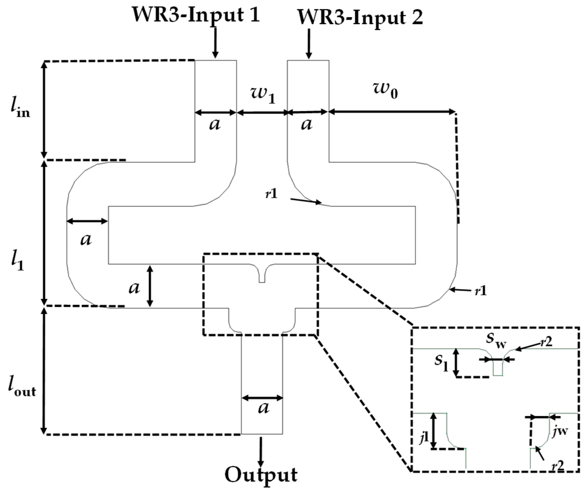
Figure 2.
Numerically analyzed S-parameters of THz 2×1 WR3-PC.
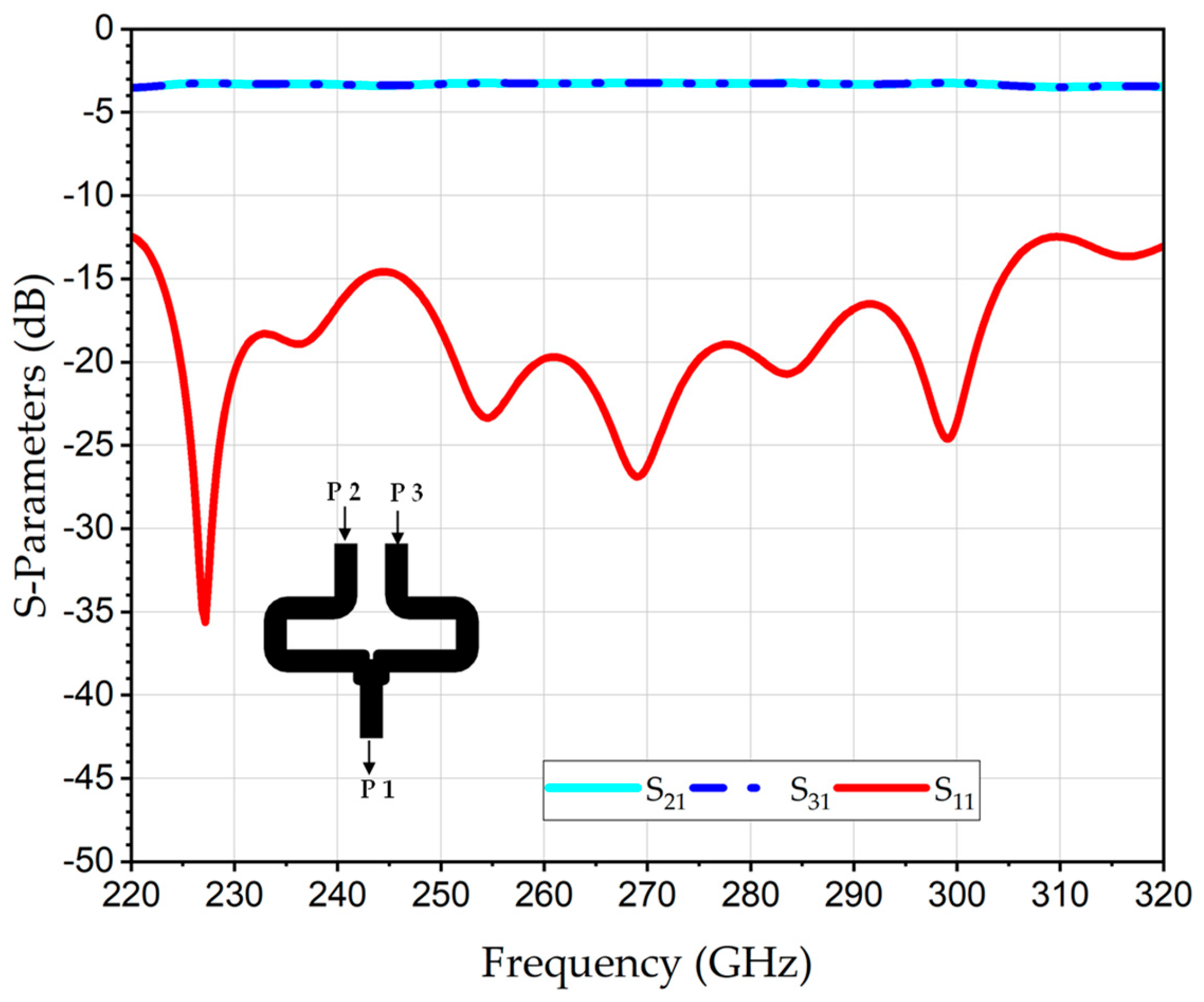
Figure 3.
Structural schematic of the polarization twister designed for WR3 waveguide interfaces, (a) Top view; (b) Cross-sectional view of the junction; (c) 3D assembly view.
Figure 3.
Structural schematic of the polarization twister designed for WR3 waveguide interfaces, (a) Top view; (b) Cross-sectional view of the junction; (c) 3D assembly view.
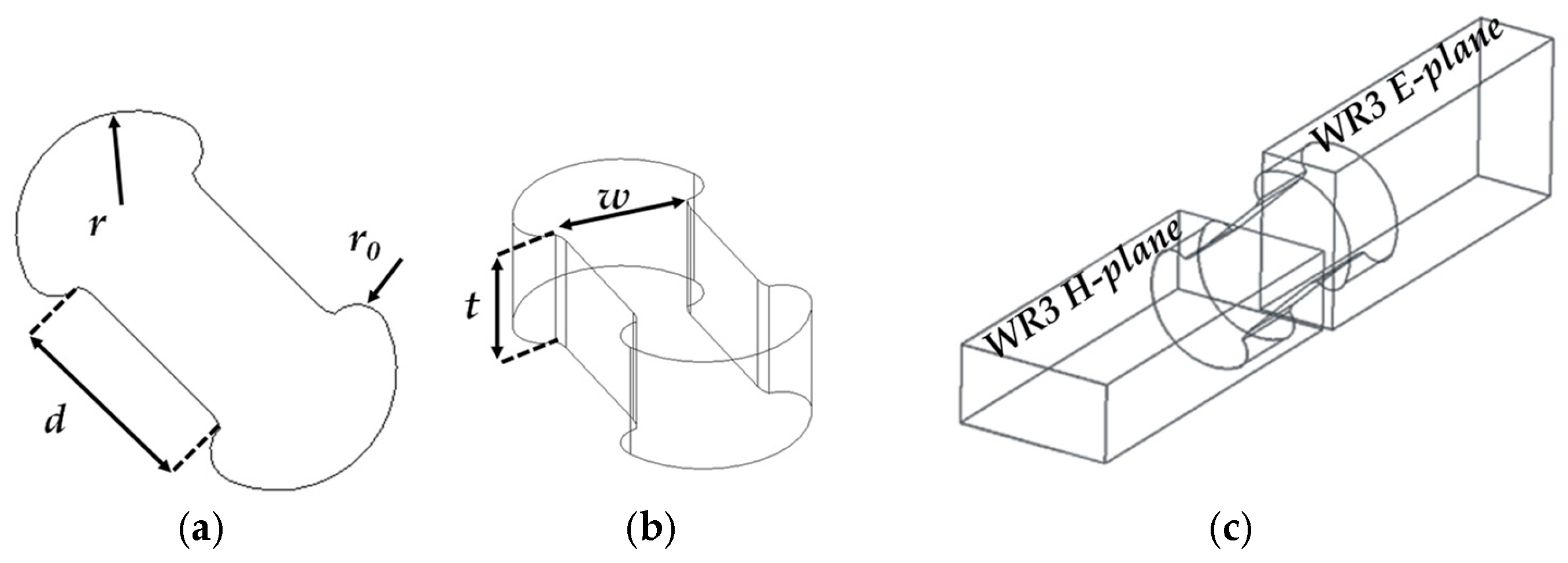
Figure 4.
Simulated S-parameters of proposed polarization twister, the 90° polarization rotation of the E-field at frequency 275 GHz, is dissipated in the inset.
Figure 4.
Simulated S-parameters of proposed polarization twister, the 90° polarization rotation of the E-field at frequency 275 GHz, is dissipated in the inset.
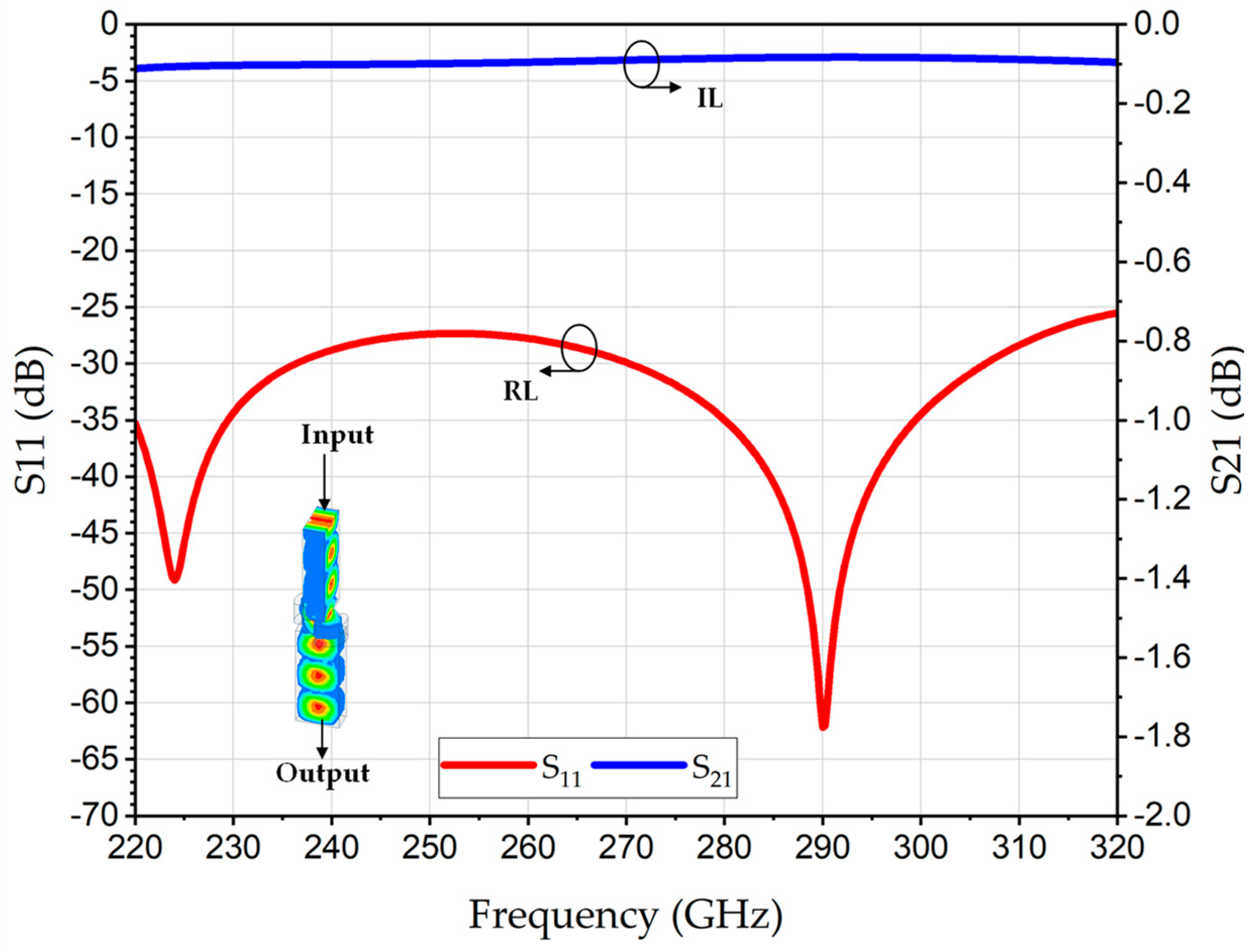
Figure 5.
3D model of a 2×2 WR3-band WR3-PC employing in H-plane.
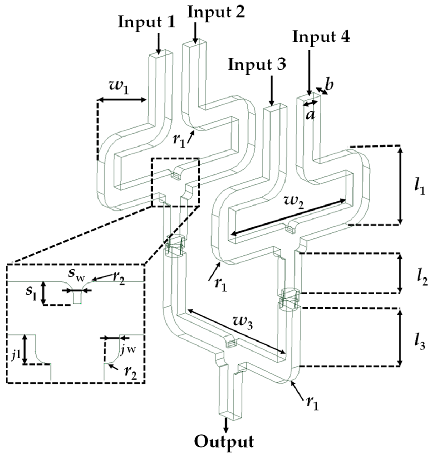
Figure 6.
Simulated S-parameters of the 2D 2×2 WR3-PC. The distribution of the E-field on between the inputs and the output at 275 GHz, is given in the inset.
Figure 6.
Simulated S-parameters of the 2D 2×2 WR3-PC. The distribution of the E-field on between the inputs and the output at 275 GHz, is given in the inset.
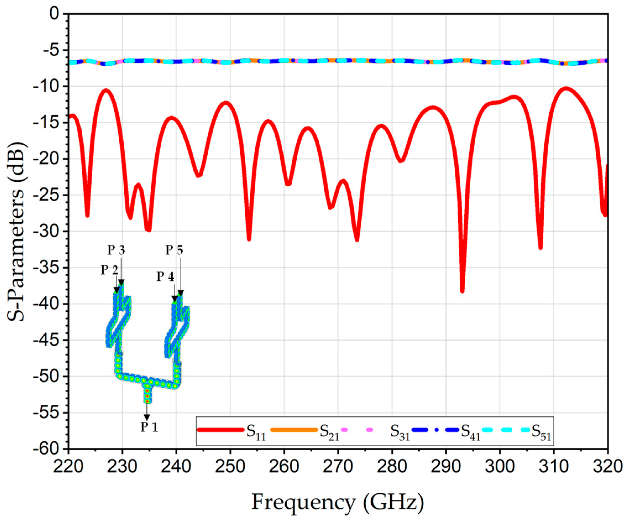
Figure 7.
3D model of a 2×4 WR3 band WG-PC employing three levels.
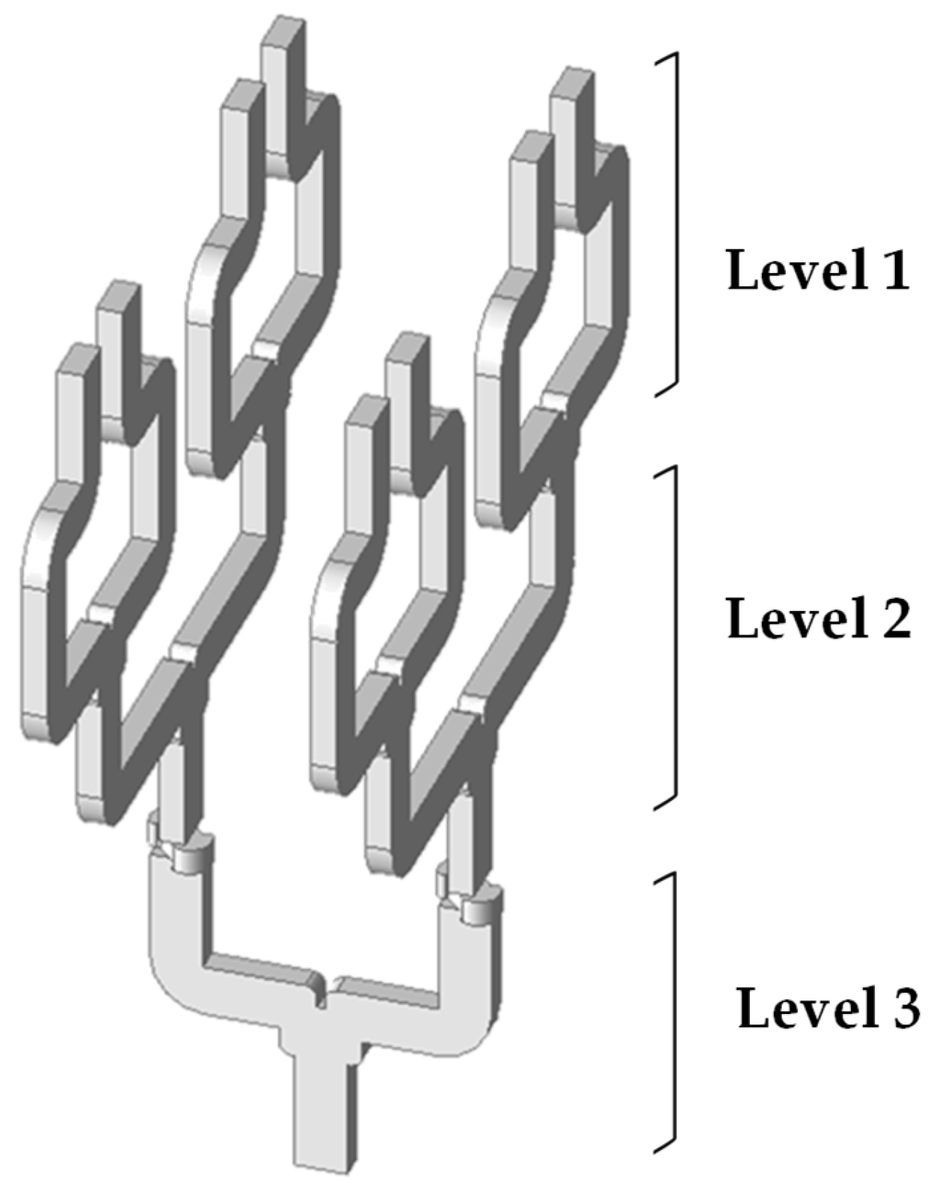
Figure 8.
Simulated S-parameters of scalable 1D levels 1 and 2 of the 2×4 WR3-PC.
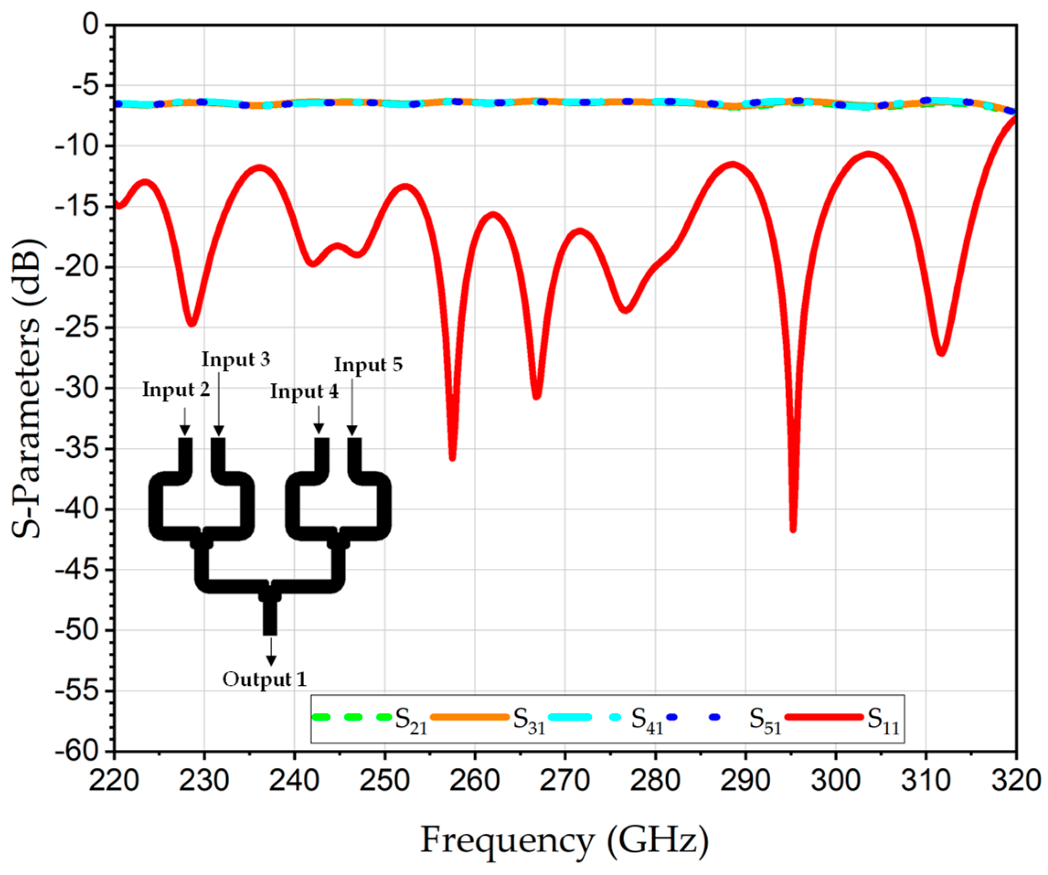
Figure 9.
Simulated S-parameters of scalable 2×4 WR3-PC.
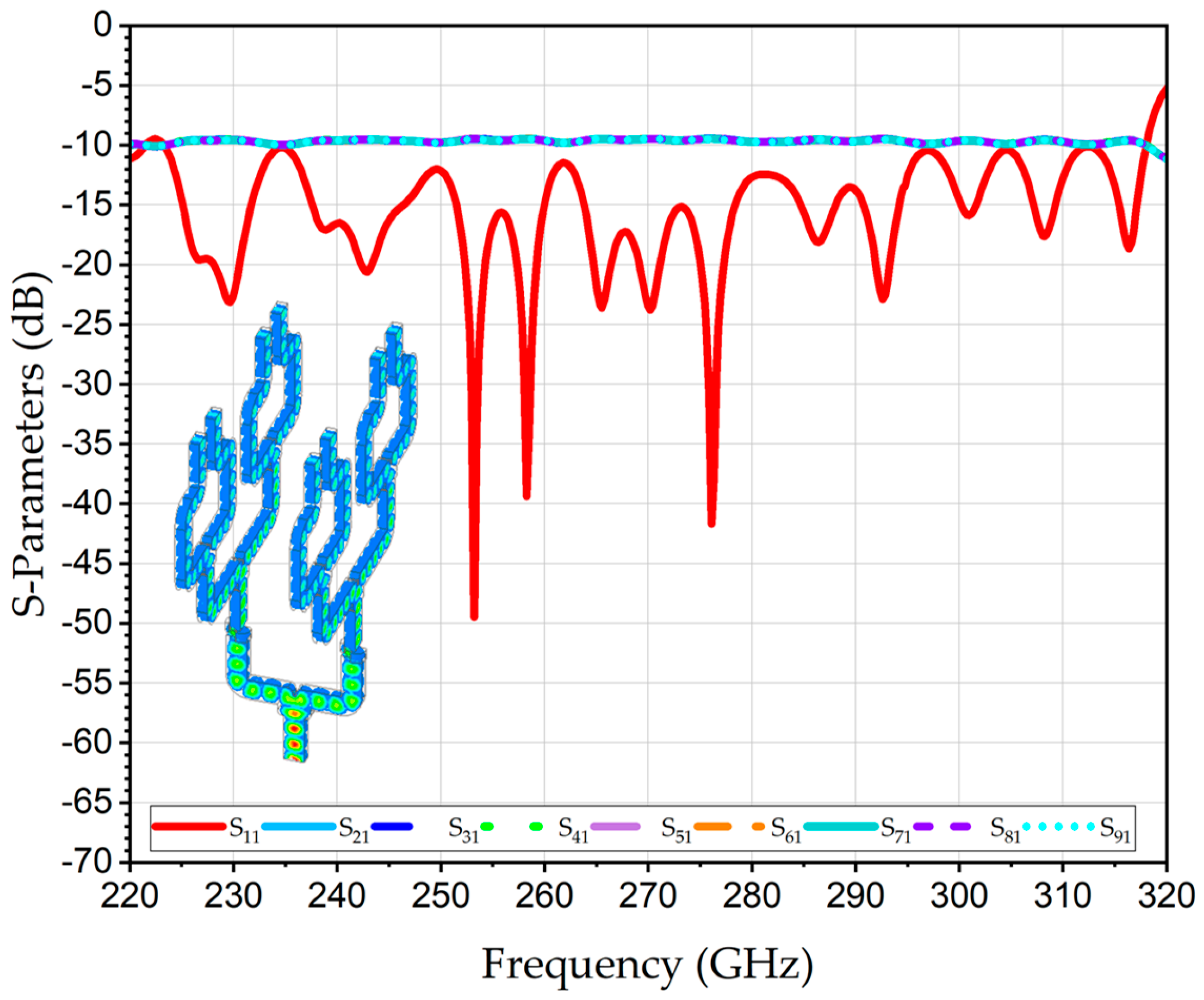
Figure 10.
Proposed integration concept of a 2D THz 2×2 WR-PC block for WR3 frequency band. The colored inset in upper right corner shows the concept of the optical coupling with an InP-based PIC of monolithically integrated an array of 2×2 THz-PDs with antennas.
Figure 10.
Proposed integration concept of a 2D THz 2×2 WR-PC block for WR3 frequency band. The colored inset in upper right corner shows the concept of the optical coupling with an InP-based PIC of monolithically integrated an array of 2×2 THz-PDs with antennas.
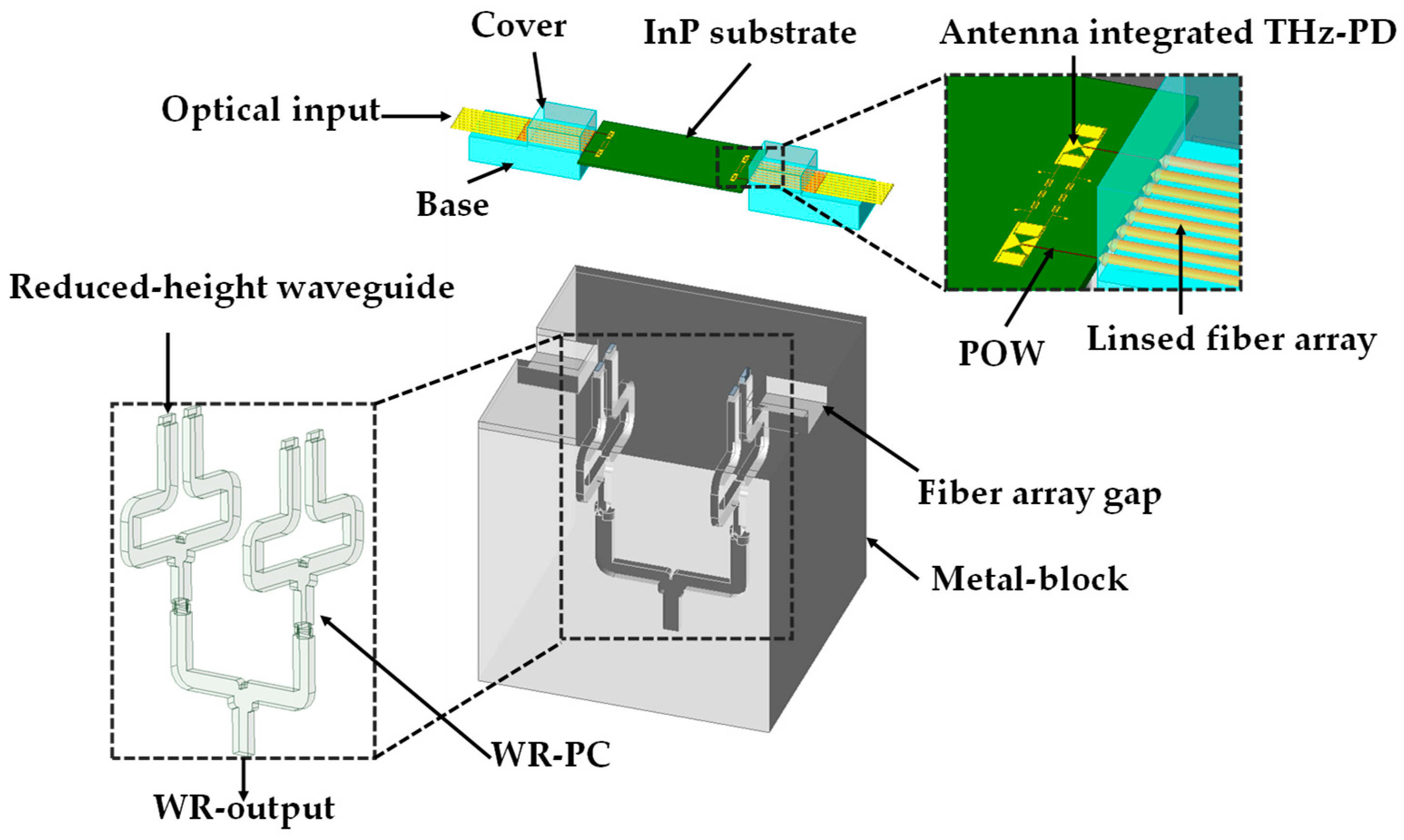
Figure 11.
Proposed InP-based slot bow-tie-to-WR3 transition: (a) top view with design parameters; (b) integration concept to WR3-waveguide.
Figure 11.
Proposed InP-based slot bow-tie-to-WR3 transition: (a) top view with design parameters; (b) integration concept to WR3-waveguide.
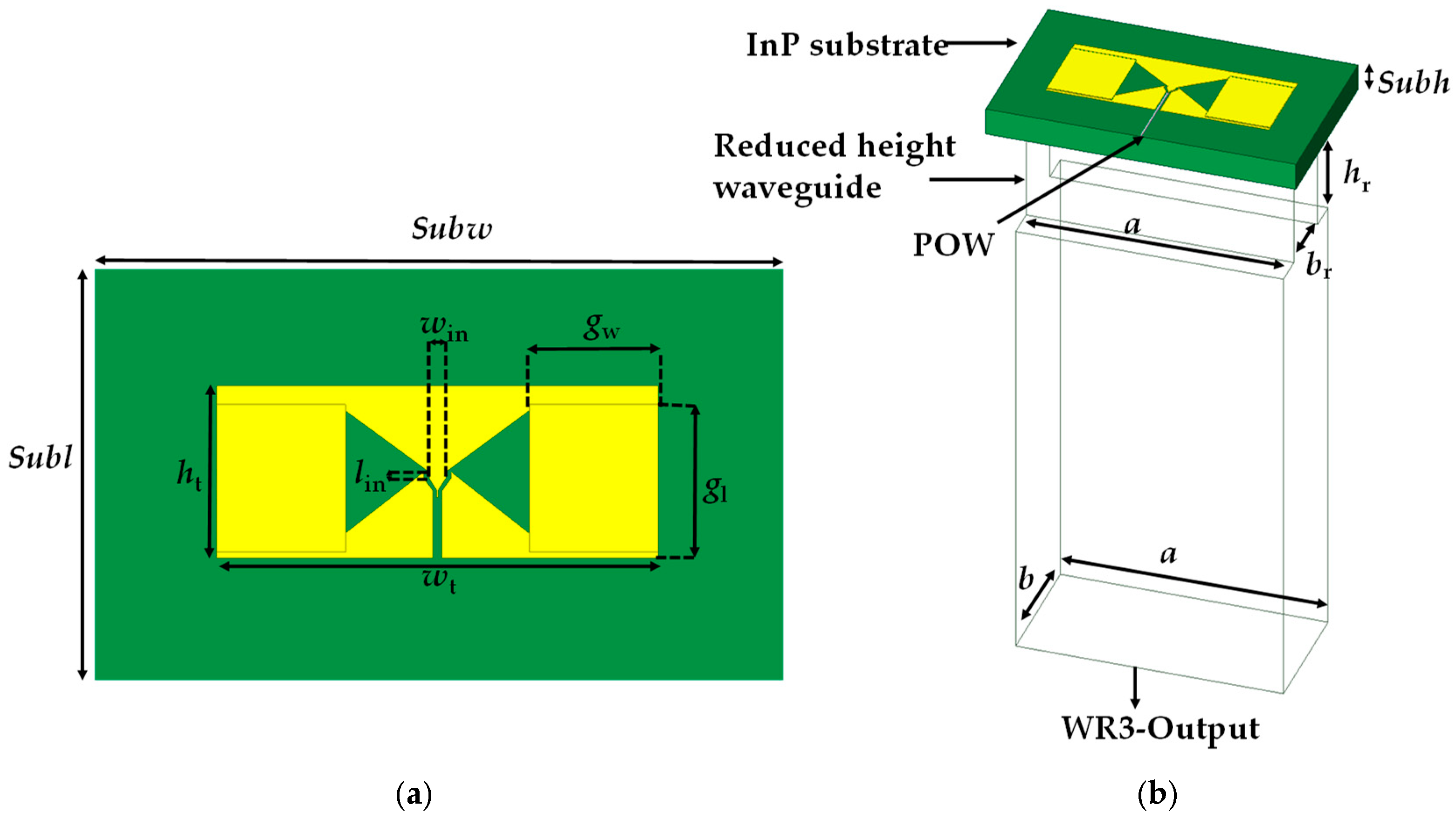
Figure 12.
Simulated S-parameters of slot bow-tie antenna on WR3-waveguide aperture. The inset shows the E-field distribution from the antenna chip to the waveguide at 275 GHz.
Figure 12.
Simulated S-parameters of slot bow-tie antenna on WR3-waveguide aperture. The inset shows the E-field distribution from the antenna chip to the waveguide at 275 GHz.
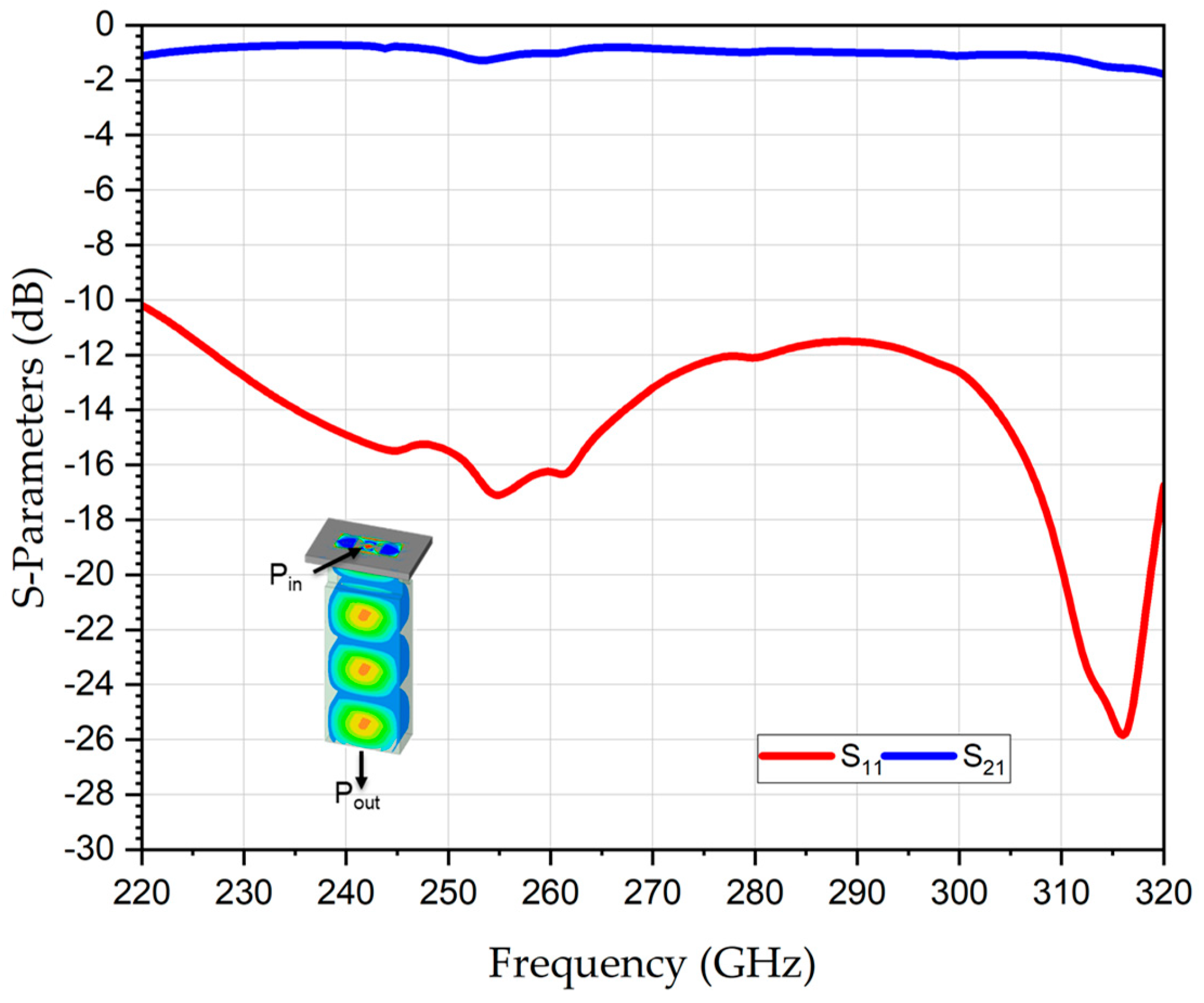
Figure 13.
Simulated S-parameters of the integration of THz-PDs array with planar array of 2×2 WR3-PC.
Figure 13.
Simulated S-parameters of the integration of THz-PDs array with planar array of 2×2 WR3-PC.
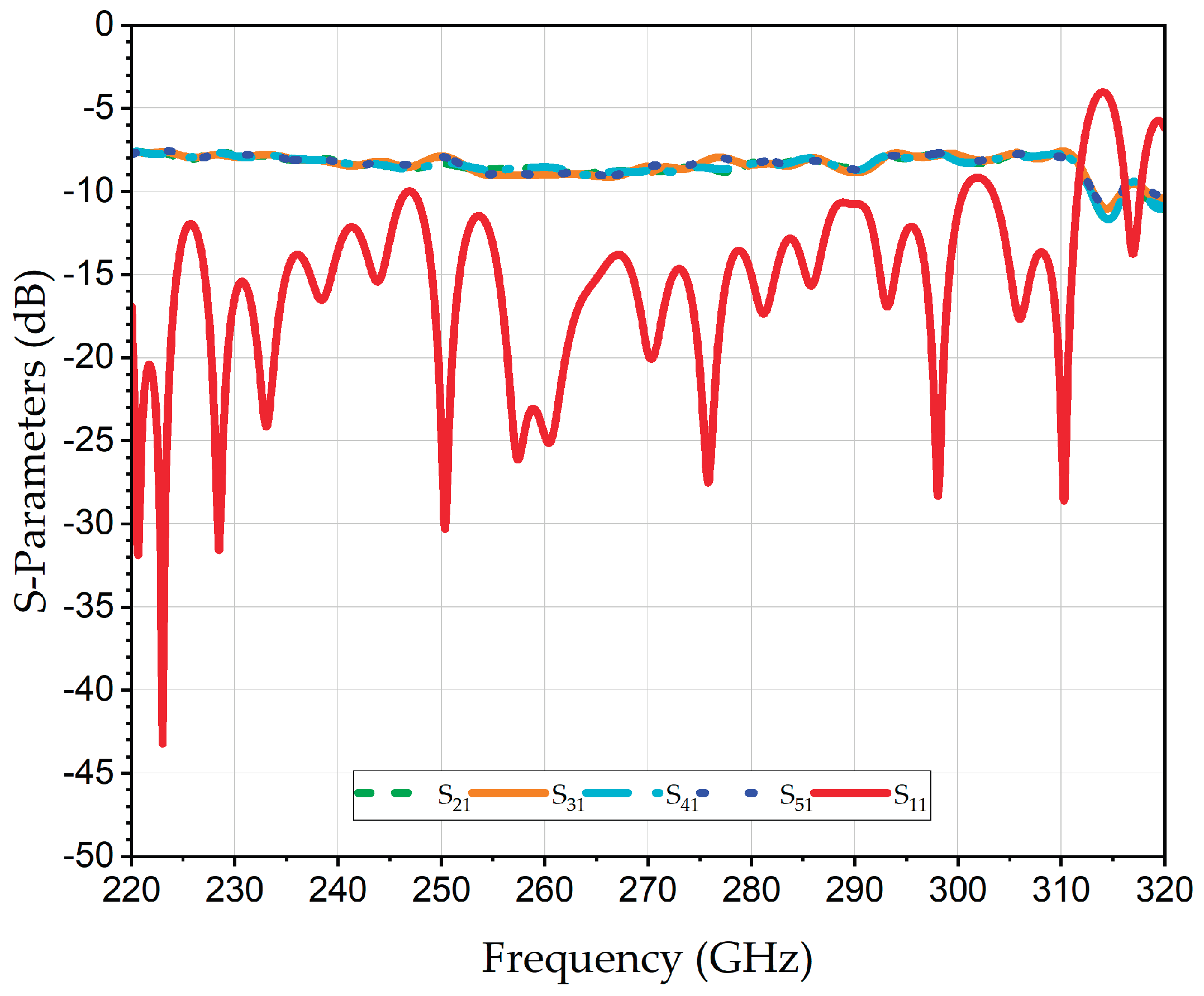

Table 1.
Numerical values of the design parameters of 2×1 WR3-PC.
| Design | Parameter | Value (mm) |
|---|---|---|
| 2×1 WR3-PC | lin | 2 |
| l1 | 2.862 | |
| lout | 2 | |
| w0 | 2.66 | |
| w1 | 1 | |
| Sw | 0.124 | |
| Sl | 0.364 | |
| jl | 0.472 | |
| jw | 0.255 | |
| r1 | 0.9 | |
| r2 | 0.2 |
Table 2.
Numerical values of design parameters of the scalable 2×2 WR-PC w.r.t to the frequency band.
Table 2.
Numerical values of design parameters of the scalable 2×2 WR-PC w.r.t to the frequency band.
|
Component |
Parameter |
Value (mm) | ||
|---|---|---|---|---|
| WR4-Band | WR3-Band | WR2.2-Band | ||
|
Twister |
r | 0.41 | 0.37 | 0.23 |
| d | 0.69 | 0.618 | 0.38 | |
| w | 0.53 | 0.4717 | 0.29 | |
| t | 0.43 | 0.43 | 0.28 | |
| r0 | 0.1 | 0.1 | 0.05 | |
|
2×2 WR3-PC |
l1 | 4 | 2 | 2.1 |
| l2 | 2.7 | 1.7 | 1.2 | |
| l3 | 2 | 1.9 | 1.38 | |
| w1 | 2.8 | 2.5 | 1.3 | |
| w2 | 6.41 | 7.8 | 2.88 | |
| w3 | 8.41 | 7.4 | 4.38 | |
| Sw | 0.126 | 0.124 | 0.1 | |
| Sl | 0.364 | 0.364 | 0.264 | |
| jl | 0.42 | 0.472 | 0.35 | |
| jw | 0.23 | 0.255 | 0.151 | |
| r1 | 1.2 | 0.9 | 0.6 | |
| r2 | 0.2 | 0.2 | 0.1 | |
Table 3.
Scalability of the 2D WR-PC Architecture.
| Nr. of inputs (n) |
Nr. of 2×1 PCs |
Nr. of polarizer |
Nr. of levels |
Tot. combining loss (dB) = Nr. levels×0.6 dB | Relative output power increase w.r.t. single input (dB) |
|---|---|---|---|---|---|
| 2 | 1 | 0 | 1 | 0.6 dB | 2.4 |
| 4 | 3 | 2 | 2 | 1.2 dB | 4.8 |
| 8 | 7 | 2 | 3 | 1.8 dB | 7.2 |
| 16 | 15 | 2 | 4 | 2.4 dB | 9.6 |
| 32 | 31 | 2 | 5 | 3 dB | 12 |
| n | n-1 | 2 |
*The reported output power represents the relative power increase compared to a single input, excluding the absolute input power.
Table 4.
Design parameters of the slot bow-tie-to-WR3 waveguide.
| Parameter | Value (µm) |
|---|---|
| hr | 380 |
| br | 240 |
| Subh | 90 |
| Subw | 1300 |
| Subl | 800 |
| win | 20 |
| lin | 17 |
| ltap | 8 |
| gw | 240 |
| gl | 230 |
| ht | 268 |
| wt | 796 |
Disclaimer/Publisher’s Note: The statements, opinions and data contained in all publications are solely those of the individual author(s) and contributor(s) and not of MDPI and/or the editor(s). MDPI and/or the editor(s) disclaim responsibility for any injury to people or property resulting from any ideas, methods, instructions or products referred to in the content. |
© 2026 by the authors. Licensee MDPI, Basel, Switzerland. This article is an open access article distributed under the terms and conditions of the Creative Commons Attribution (CC BY) license (http://creativecommons.org/licenses/by/4.0/).
Copyright: This open access article is published under a Creative Commons CC BY 4.0 license, which permit the free download, distribution, and reuse, provided that the author and preprint are cited in any reuse.


