Submitted:
28 January 2026
Posted:
29 January 2026
You are already at the latest version
Abstract
In the AI era of big data explosion, similarity search—a core task in machine learning and data mining—requires high speed, energy efficiency, and scenario adaptability. Conventional electronic CAMs face RC delay bottlenecks, while existing OCAMs are limited by fixed bit-widths and limited distance metrics. Here, we demonstrate a variable bit-width all-optical CAM architecture employing phase-change material Sb₂Se₃ integrated with Mach-Zehnder Interferometers (MZIs). The proposed multi-segment memory unit (MSMU) compresses N-bit binary data into a single analog photonic unit, supporting direct data writing/loading without DACs and flexible trade-offs between precision, storage capacity, noise immunity, and energy, while enabling Hamming and non-linear (NL) distance calculations. A 6-element 3-bit OCAM fabricated on a SiN-SOI platform realizes reliable storage and retrieval. kNN simulations on iris, wine, and breast cancer datasets show that the 3-bit mode achieves accuracy comparable to Manhattan/Euclidean distances under high SNR, while the 1-bit mode offers robust noise immunity. Energy consumption is 364 fJ/bit (3-bit) and 890 fJ/bit (1-bit). This architecture provides a high-speed, energy-efficient, and flexible all-optical similarity search solution, promising wide applications in machine learning and data mining.
Keywords:
all-optical content-addressable memory
; phase-change materials
; similarity search
; kNN
1. Introduction
In the artificial intelligence era, the explosive growth of big data has established similarity search as a fundamental task across machine learning, recommendation systems, and data mining. This imposes increasingly stringent demands not only on processing speed and energy efficiency, but also on adaptability to diverse application scenarios [1,2]. The core operation of similarity search involves calculating the distance (or similarity) between a search vector and all vectors stored in memory. Conventional memory systems rely on address-based access, necessitating sequential data retrieval and subsequent computation. In contrast, CAMs offer a parallel search mechanism by comparing the input search vector against all stored entries simultaneously and returning the address of any matching content, thereby significantly accelerating search operations and improving energy efficiency [3,4,5,6,7]. The underlying matching operation in CAMs is typically based on calculating the Hamming distance between binary vectors, and numerous studies have implemented similarity search using electronic CAMs [8,9,10,11,12,13,14,15,16,17]. However, electronic CAMs face an inevitable bottleneck: resistance-capacitance (RC) delay severely constrains their operating speed [18].
Optical computing has emerged as a promising alternative to electronic computing due to its inherent high speed, low power consumption, and parallel processing capabilities [19,20,21]. Several optical CAMs (OCAMs) utilizing photonic matching structures have been proposed to overcome the limitations of electronic CAMs. For instance, OCAMs employing InP-based flip-flops for data loading and SOA-MZI-based XOR gates for bitwise comparison have been demonstrated [22,23,24]. Another common approach exploits the resonant states of microring resonators for matching [25,26,27]: transmission is suppressed when the input wavelength aligns with the ring’s resonance, whereas a detuned state allows light to pass through. By performing the matching operation directly in the optical domain, such OCAMs can achieve search rates up to 10 Gb/s. A critical limitation, however, is that they still rely on electronic memory, imposing an additional energy overhead to maintain the stored data state on optical devices during queries.
Non-volatile phase-change materials (PCMs) offer a promising solution to this problem. PCMs exhibit reversible phase transitions between amorphous and crystalline states, accompanied by a significant contrast in both the refractive indices (n) and extinction coefficients (k). This property has enabled their use in optical memories and photonic in-memory computing [28,29,30,31]. Recently, all-optical CAMs with non-volatile optical storage have been realized using Ge2Sb2Te5 (GST), a representative PCM, -based microring resonators [32] and MZIs [33], respectively. Notably, all existing OCAMs perform bit-wise matching, which ensures matching precision but lacks the flexibility required for diverse tasks. For example, routing lookups [34] demands exact matching, whereas recommendation systems [35] can tolerate approximate results. Bioinformatics applications like DNA classification [14] rely on Hamming distance calculation for binary data, while other tasks (e.g., iris recognition) involve continuous data and may require various distance metrics, including Hamming, Manhattan, and Euclidean distances. Furthermore, most existing OCAMs typically output only the Hamming distance, offering limited functional versatility.
In this work, we propose and demonstrate a variable bit-width all-optical CAM architecture based on MZIs and the low-loss Sb2Se3. Sb2Se3 exhibits an ultra-low extinction coefficient (k<10-5) across the telecommunications transmission band, making it highly suitable for low-loss photonic device [36]. By integrating multiple independently programmable Sb2Se3 segments and phase shifters on the arms of an MZI, the system can adaptively trade off matching precision against storage capacity, while also supporting enhanced functional flexibility. The similarity between the search and stored data is encoded in the output optical power of the MZI. We designed and fabricated a 6-element, 3-bit OCAM on a SiN-SOI platform, experimentally validating its matching functionality and further demonstrating through simulations its applicability to kNN classification across multiple datasets.
2. Principle
The design philosophy of this study is to compress the data that would otherwise occupy multiple binary memory units into a single analog unit. Meanwhile, the direct writing and loading of binary data are realized via multi-segment memory and modulation technology, without the need for any additional configuration of digital-to-analog converter (DAC) hardware. As shown in Figure 1(a), the multi-segment memory unit (MSMU) is based on an MZI, consisting of a beam splitter, a directional coupler, and two optical waveguides (arms) between them. Each arm is integrated with Sb2Se3 cells and phase shifters, divided into N segments. In the i-th segment ( ), there are Sb2Se3 cells dedicated to storing the i-th bit of the N-bit data . Correspondingly, the phase shifter length is for loading the i-th bit of the N-bit search data, where is the minimum length of the phase shifter. Moreover, the phase shift generated by the phase shifter with length is equal to that generated by a single Sb2Se3 cell, denoted as .
The output optical power of the MZI is determined by the phase difference between the two arms, following the interference formula:
where is the input optical power. When the stored data x matches the search data s, the output optical power reaches maximum/minimum; the lower the similarity, the larger the deviation from matching extremum. To ensure an accurate mapping relationship, the total phase shift must not exceed (i.e., ). By adjusting the number of Sb2Se3 cells and phase shifter length in each segment, binary numbers are weight-mapped to phase shifts according to bit significance, enabling analog subtraction. Note that the mapping of binary data (0 and 1) depends on the implementation of the phase shifter in the search arm: for example, the refractive index increases with temperature in thermo-optic effects but decreases with voltage in electro-optic effects, resulting in inverted data mapping. Combining the output ports of M MSMUs enables searching match and similarity calculation for M-element N-bit vectors as shown in Figure 1(b).
Notably, while previous studies used GST for non-volatile OCAMs, it is unsuitable for this device. As mentioned earlier, GST exhibits a non-negligible, state-dependent extinction coefficient, meaning the MZI output power is simultaneously affected by phase difference and loss variations. This complicates establishing an accurate mapping between output power and data similarity for multi-segment configurations. Although storing and searching data via GST is a potential solution, the search speed is limited by GST’s switching speed ( 100 ns), and significant loss restricts the number of segments. In contrast, Sb2Se3’s ultra-low extinction coefficient makes it an excellent choice for non-volatile reconfigurable phase tuning, and it has been widely used in various reconfigurable photonic devices [37,38,39,40,41,42].
Obviously, the greater the number of segments, the smaller the step sizes between output power levels, the lower the noise immunity, and the higher the memory capacity. Thus, for precision-sensitive matching or similarity calculation tasks, data can be distributed across multiple MSMUs to reduce the bit-width per MSMU, thereby improving precision, as shown in Figure 2(a). Prioritizing high-bit segments when reducing the bit-width increases the step size between levels. In the extreme case, 1-bit operation can be achieved, which is consistent with previous studies. Alternatively, it is also feasible to employ more segments when operating at a low bit-width. For instance, all segments can be utilized at the 1-bit-width mode to fully exploit the extinction ratio of the Mach-Zehnder Interferometer (MZI). The advantage of this approach is that higher noise immunity can be achieved; however, driving N phase shifters simultaneously will lead to a significant increase in power consumption. This involves a trade-off between performance and power consumption when catering to different environmental and application requirements, and the subsequent work of this paper still adopts the configuration illustrated in Figure 2(a).
A more detailed illustration, taking the 3-bit-width and 1-bit-width as examples, is presented in Figure 2(b). For scalar search, the 3-bit-width mode can directly yield an analog nonlinear distance (NL-distance) via the MSMU, and is also capable of performing match search with a comparator to output a digital match state; in contrast, the 1-bit-width mode directly outputs the Hamming distance, while match search can be equally realized using a comparator. In addition, for vector search, the 3-bit-width mode enables separate aggregation of the two types of outputs derived from scalar search, thus yielding both the NL-distance and Hamming distance of the vector, whereas the 1-bit-width mode can only obtain the vector Hamming distance by summing the scalar match results.
3. Results and Discussion
3.1. Fabrication
A 6-MSMU optical CAM was designed and fabricated on a SiN-SOI platform [Figure 3(a)]. The silicon nitride single-mode waveguide has a width of 1000 nm and a thickness of 400 nm. After being split by a Y-junction waveguide, the input light undergoes interference in a 2×2 multimode interferometer (MMI). One of the output ports is connected to a 6×1 MMI for combining the output signals of other MSMUs, corresponding to Port A in Figure 2(b); the other port is routed directly to a grating coupler, which can be connected to a comparator following photoelectric conversion, corresponding to Port D in Figure 2(b). For the Sb2Se3 cells, the silica cladding above the waveguide was etched (oxide window opening), followed by deposition of a 30-nm-thick Sb2Se3 layer and a 10-nm-thick silica capping layer. Figure 3(b) shows a scanning electron microscope (SEM) image of the 6×1 MMI and oxide windows. Each cell has an oxide window size of 5 µm × 10 µm, in which Sb2Se3 is fully deposited. A total of 34 Sb2Se3 cells are integrated on each arm, with some used for data storage and others for initial state calibration and standby. Due to experimental constraints, optoelectronic phase shifters were not integrated; instead, Sb2Se3 cells were used as substitutes. The feasibility for high-speed multi-segment phase shifting has been validated in previous optical digital-to-analog converter (ODAC) studies [43,44,45].
3.2. Results
The experimental setup [Figure 3(c)] includes a multi-channel laser, an optical power meter and a spatial light focusing system (for controlling Sb2Se3 cells). The spatial light focusing system irradiates Sb2Se3 cells with 532-nm laser pulses (500 ms , ∼ 7mW) via an objective lens to switch their phase states [36]. Each irradiation is performed with only a single pulse.
To characterize the phase tuning capability of Sb2Se3 cells, a single arm of the MZI was tested [Figure 4(a)]. Sb2Se3 cells were irradiated sequentially; the sweep results show that 11 Sb2Se3 cells produce a phase shift exceeding , limiting the maximum 3 bit width for subsequent experiments. We tested the Sb2Se3 cells on 6 MSMUs, and estimated the phase shift generated by each Sb2Se3 cell via curve fitting. Statistical results demonstrate that the Sb2Se3 cells exhibit favorable consistency, as shown in Figure 4(b). Next, the bit precision of MSMU was tested for 1-bit, 2-bit, and 3-bit configurations [Figure 4(c)]. Each level was measured 10 times with different devices, and the results confirm that stored data can be reliably identified even at 3 bits, although higher bit-widths exhibit reduced noise immunity and interference resistance.
We irradiated 1, 4, and 7 Sb2Se3 cells on one arm of each of the three MSMUs, corresponding to the stored data values of 1, 4, and 7 respectively. On the other arm, we sequentially irradiated 7 Sb2Se3 cells, scanned to obtain the NL-distances for different search values, and determined the matching status via threshold judgment. Figure 4(d) shows search results; although the output power for matching queries is close to that of adjacent values, reliable discrimination is still achievable.
As noted previously, the switching speed of Sb2Se3 cells is very slow (500 ms-width switching laser pulse), and the limited number of fabricated devices fails to meet the required dataset size. To validate the architecture’s performance in similarity search, kNN simulations were conducted based on statistical phase shift data of Sb2Se3 cells. In the simulations, the extinction ratio of the MZI was set to 20 dB, with random noise added when loading search data into the phase shifters. We implemented classification tasks via the kNN algorithm based on the iris, wine, and breast cancer datasets, respectively. As shown in Figure 5(a), to adapt to the work presented in this paper, the feature values of all data were quantized to 3 bits. Then, all datasets are randomly divided into a training set and a test set in a ratio of 7:3.
Based on the vector search depicted in Figure 2(b), we simulated three search results under the 1-bit-width and 3-bit-width modes, denoted as 1-bw HD, 3-bw HD and 3-bw NL respectively. To obtain more objective results, we scanned the k from 1 to 15, conducted 100 random tests for each configuration to derive the average accuracy, and then selected the optimal results from those corresponding to all k values. The relationship between the simulation results of the three datasets, the signal-to-noise ratio (SNR) applied to the phase shifters, as well as three theoretically calculated benchmarks are presented in Figure 5(b–d). It is evident that the Manhattan distance and Euclidean distance are more suitable for kNN than the Hamming distance. At relatively high SNR levels, 1-bw HD yields results consistent with the Hamming distance, and the same applies to 3-bw HD, while the latter imposes a higher requirement on SNR. In contrast, 3-bw NL is closer to the Manhattan distance and Euclidean distance, which achieve higher accuracy—or more precisely, closer to the Euclidean distance (pronounced in the wine dataset). This may be attributed to the fact that both the NL-distance and Euclidean distance exhibit concave curves in the near-zero interval. At relatively low SNR levels, 1-bw HD outperforms 3-bw HD by a significant margin, which is consistent with the noise immunity characteristics analyzed earlier. However, 3-bw NL, which also has poor noise resistance, exhibits mixed performance relative to 1-bw HD across different datasets, a phenomenon that may benefit from its adoption of a more suitable distance function.
The above experimental results indicate that storing multi-bit information in a single MSMU improves memory capacity, or equivalently memory density, at the cost of certain noise immunity and computational accuracy. However, in scenarios with high SNR or in applications with error tolerance such as kNN, the obtained results can be comparable to those of the theoretical distance algorithm. Therefore, we can perform flexible configuration according to different operating environments and application scenarios to achieve a trade-off between noise immunity and memory capacity, as well as the selection of different distance functions.
3.3. Energy estimation
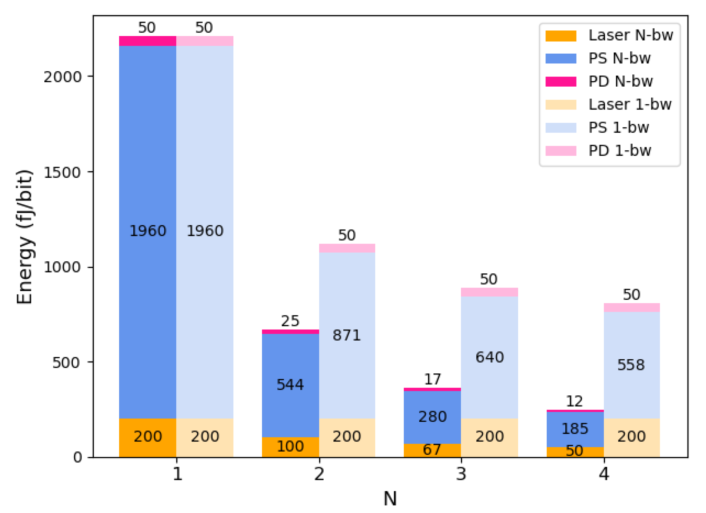
Considering the trade-off between search speed and energy consumption, and with reference to the general performance of existing OCAMs, the phase shifter speed is set to 10 Gb/s, which is much lower than the limit speed of the optical digital-to-analog converter (ODAC) [45]. The system energy consumption is evaluated under the above conditions. The total power consumption is given by:
where is the input optical power, WPE is the wall-plug efficiency of laser source, and and , are the power consumptions of the phase shifter and photodetector, respectively. Assuming an MZI extinction ratio of 20 dB and a photodetector sensitivity of -25 dBm [46], the minimum is 0.32 mW with a WPE of 16% [47]. Ref. [48] demonstrated a PN silicon-based MZI with a of 0.07 V·cm. To avoid crosstalk between the phase shifters and Sb2Se3 cells, it is assumed that each MSMU employs a single-arm phase shifter with a total length of 1 mm, yielding a of 1.4 V. The operating voltage of the i-th phase shifter segment is thus given by V. Under the conditions of uniform data distribution (equal numbers of 0 and 1) and a resistance of 50 , the power consumption is calculated as W. The is set to 3 mW [46]. For the structure fabricated in this work where and , the power consumption values are 364 fJ/bit and 890 fJ/bit for the 3-bit-width and 1-bit-width modes, respectively. In comparison, a recently demonstrated O-TCAM based on a heterogeneous III-V/Si microrings exhibits an energy consumption of 703 fJ/bit [49]. It is evident that the impact of M on the energy consumption per bit is only reflected in the PD, and the is relatively low. Therefore, we only evaluate the impact of the bit-width N on power consumption, as illustrated in Figure 6, where the deep color blocks represent the N-bit-width mode and the light blocks represent the 1-bit-width mode. Notably, the power consumption of the phase shifters, which accounts for the largest proportion, decreases with the increase of N, since the multi-segment electrodes share the .
3.4. Discussion
Despite discrepancies between the fabricated device and the target design, the experiments validate the feasibility of the proposed architecture. However, it also has to address other challenges. Currently, phase shifters generally have relatively long lengths, and the multi-segment structure requires additional consideration of crosstalk effects, resulting in low integration density. As the bit-width increases, the number of required Sb2Se3 cells grows exponentially, and errors caused by the randomness of state switching accumulate accordingly. Furthermore, the nonlinearity of MZIs makes precise matching more challenging due to noise and randomness, which is more pronounced at high bit-widths. Three feasible optimization directions are identified:
- 1.
- Reducing footprint and energy consumption. Indium Tin Oxide (ITO) is a promising active material that enables high refractive index modulation. Ref. [50] demonstrated a heterogeneously integrated ITO plasmonic MZI modulator on an SOI platform, whose experimental characterization revealed that a phase shift is achievable with a device length on the micrometer scale, alongside an ultra-low of 95 V·µm. Furthermore, Ref. [51] demonstrated the 100 GHz modulation capability of an ITO-based MZI.
- 2.
- Improving noise immunity. Due to the presence of noise, MZI nonlinearity poses challenges for high bit-width operations, particularly near matching conditions where adjacent levels are closely spaced. Previous work [52] demonstrated that optimizing phase shifter lengths and control vectors can eliminate nonlinearity and improve ODAC bit-width, which is applicable to this architecture.
- 3.
- Reducing randomness. For the study reported in this paper, the 5-µm-wide Sb2Se3 cells utilized in experiments are of overly large dimensions. A phase shift close to would be induced by the complete crystallization of the whole cell. As a result, only a small localized area within the cell was subjected to partial crystallization via a single pulse, which introduced non-negligible randomness to the experimental data. The adoption of Sb2Se3 cells with reduced dimensions is anticipated to diminish randomness through full crystallization, while simultaneously facilitating higher-precision phase tuning and enabling support for larger bit-widths.
4. Conclusions
This work proposes and demonstrates a variable bit-width all-optical CAM based on MZIs and Sb2Se3, addressing the limitations of conventional optical and electronic CAMs such as fixed bit-widths and limited functionality. The core multi-segment memory unit (MSMU) compresses multi-bit binary data into a single analog unit, enabling direct data writing/loading without digital-to-analog converters, flexible bit-width adjustment, and support for both Hamming distance and NL-distance calculations. Experimental validation of a 6-element 3-bit OCAM fabricated on a SiN-SOI platform confirms reliable matching performance, while kNN simulations on iris, wine, and breast cancer datasets demonstrate that the 3-bit-width mode achieves accuracy comparable to Manhattan and Euclidean distances under high SNR, and the 1-bit-width mode offers robust noise immunity. Energy estimation shows superior efficiency (364 fJ/bit for 3-bit-width) compared to state-of-the-art OCAMs. Despite challenges including low integration density, Sb2Se3 state switching randomness, and MZI nonlinearity, future optimizations using ITO phase shifters, phase parameter tuning, and miniaturized Sb2Se3 cells are promising. This work provides a flexible, high-density, and energy-efficient solution for all-optical similarity search, with broad potential in big data analytics and artificial intelligence applications.
Author Contributions
Conceptualization, Y.G.; methodology, Y.G.; software, Y.G.; validation, Y.G. and Y.Z.; formal analysis, Y.G. and G.Y.; investigation, Y.G. and H.G.; resources, X.H. and B.S.; data curation, Y.G. and Y.Z.; writing—original draft preparation, Y.G.; writing—review and editing, Y.G. and H.G.; visualization, Y.G.; supervision, H.G. and B.S.; project administration, J.W. and Q.L. All authors have read and agreed to the published version of the manuscript.
Funding
This research was funded by National Key Research and Development Program of China (2022YFA1203700)
Institutional Review Board Statement
Not applicable.
Informed Consent Statement
Not applicable.
Data Availability Statement
The original contributions presented in this study are included in the article. Further inquiries can be directed to the corresponding author.
Conflicts of Interest
The authors declare no conflicts of interest.
Abbreviations
The following abbreviations are used in this manuscript:
| AI | Artificial intelligence |
| CAM | Content-addressable memory |
| MZI | Mach-Zehnder Interferometer |
| DAC | Digital to analog converter |
| SOI | Silicon-on-Insulator |
| kNN | k Nearest Neighbors |
| SiN | Silicon nitride |
| SOA | Semi-conductor Optical Amplifier |
| PCM | Phase-change material |
| RC | Resistance-capacitance |
| SEM | Scanning electron microscope |
| MMI | Multimode interferometer |
| SNR | Signal-to-noise ratio |
| WPE | Wall-plug efficiency |
| ITO | Indium Tin Oxide |
References
- Zhang, J.; Tang, J.; Ma, C.; Tong, H.; Jing, Y.; Li, J.; Luyten, W.; Moens, M.F. Fast and Flexible Top-k Similarity Search on Large Networks. ACM Trans. Inf. Syst. 2017, 36. [Google Scholar] [CrossRef]
- Rakthanmanon, T.; Campana, B.; Mueen, A.; Batista, G.; Westover, B.; Zhu, Q.; Zakaria, J.; Keogh, E. Addressing Big Data Time Series: Mining Trillions of Time Series Subsequences Under Dynamic Time Warping. ACM Trans. Knowl. Discov. Data 2013, 7. [Google Scholar] [CrossRef]
- Jin, C.; Xu, J.; Zhao, J.; Gu, J.; Chen, J.; Liu, H.; Qian, H.; Zhang, M.; Chen, B.; Cheng, R.; et al. A Multi-Bit CAM Design With Ultra-High Density and Energy Efficiency Based on FeFET NAND. IEEE Electron Device Letters 2023, 44, 1104–1107. [Google Scholar] [CrossRef]
- Xu, W.; Luo, J.; Chen, Z.; Fu, B.; Fu, Z.; Wang, K.; Huang, Q.; Huang, R. A Novel Ferroelectric FET Based Universal Content Addressable Memory With Reconfigurability for Area- and Energy-Efficient In-Memory-Searching System. IEEE Electron Device Letters 2024, 45, 1345–1348. [Google Scholar] [CrossRef]
- Imani, M.; Peroni, D.; Rahimi, A.; Rosing, T.S. Resistive CAM Acceleration for Tunable Approximate Computing. IEEE Transactions on Emerging Topics in Computing 2019, 7, 271–280. [Google Scholar] [CrossRef]
- Mujahid, O.; Ullah, Z. High Speed Partial Pattern Classification System Using a CAM-Based LBP Histogram on FPGA. IEEE Embedded Systems Letters 2020, 12, 87–90. [Google Scholar] [CrossRef]
- Wang, X.; Qu, Y.; Yang, F.; Zhao, L.; Lee, C.; Zhao, Y. A Highly Compact Nonvolatile Ternary Content Addressable Memory (TCAM) With Ultralow Power and 200-ps Search Operation. IEEE Transactions on Electron Devices 2022, 69, 4259–4264. [Google Scholar] [CrossRef]
- Pedretti, G.; Graves, C.E.; Serebryakov, S.; Mao, R.; Sheng, X.; Foltin, M.; Li, C.; Strachan, J.P. Tree-based machine learning performed in-memory with memristive analog CAM. Nature communications 2021, 12, 5806. [Google Scholar] [CrossRef] [PubMed]
- Wang, F.; Zhang, W.; Li, Z.; Lin, N.; Bao, R.; Xu, X.; Dou, C.; Wang, Z.; Shang, D. In-memory search with learning to hash based on resistive memory for recommendation acceleration. npj Unconventional Computing 2024, 1, 10. [Google Scholar] [CrossRef]
- Pedretti, G.; Böhm, F.; Bhattacharya, T.; Heittmann, A.; Zhang, X.; Hizzani, M.; Hutchinson, G.; Kwon, D.; Moon, J.; Valiante, E.; et al. Solving Boolean satisfiability problems with resistive content addressable memories. npj Unconventional Computing 2025, 2, 7. [Google Scholar] [CrossRef]
- Feldmann, J.; Youngblood, N.; Li, X.; Wright, C.D.; Bhaskaran, H.; Pernice, W.H.P. Integrated 256 Cell Photonic Phase-Change Memory With 512-Bit Capacity. IEEE Journal of Selected Topics in Quantum Electronics 2020, 26, 1–7. [Google Scholar] [CrossRef]
- Yang, R.; Li, H.; Smithe, K.K.; Kim, T.R.; Okabe, K.; Pop, E.; Fan, J.A.; Wong, H.S.P. Ternary content-addressable memory with MoS2 transistors for massively parallel data search. Nature Electronics 2019, 2, 108–114. [Google Scholar] [CrossRef]
- Ni, K.; Yin, X.; Laguna, A.F.; Joshi, S.; Dünkel, S.; Trentzsch, M.; Müller, J.; Beyer, S.; Niemier, M.; Hu, X.S.; et al. Ferroelectric ternary content-addressable memory for one-shot learning. Nature Electronics 2019, 2, 521–529. [Google Scholar] [CrossRef]
- Garzón, E.; Golman, R.; Jahshan, Z.; Hanhan, R.; Vinshtok-Melnik, N.; Lanuzza, M.; Teman, A.; Yavits, L. Hamming Distance Tolerant Content-Addressable Memory (HD-CAM) for DNA Classification. IEEE Access 2022, 10, 28080–28093. [Google Scholar] [CrossRef]
- Lee, J.S.; Yoon, J.; Choi, W.Y. In-Memory Nearest Neighbor Search With Nanoelectromechanical Ternary Content-Addressable Memory. IEEE Electron Device Letters 2022, 43, 154–157. [Google Scholar] [CrossRef]
- Garzón, E.; Golman, R.; Lanuzza, M.; Teman, A.; Yavits, L. A Low-Complexity Sensing Scheme for Approximate Matching Content-Addressable Memory. IEEE Transactions on Circuits and Systems II: Express Briefs 2023, 70, 3867–3871. [Google Scholar] [CrossRef]
- Gao, G.; Wen, B.; Yang, N.; Du, Z.; Jiang, M.; Mao, R.; Qiu, R.; Cao, Y.; Xue, H.; Zou, D.; et al. Sb-contacted MoS2 flash memory for analogue in-memory searches. Nature Nanotechnology 2025, 1–9. [Google Scholar] [CrossRef]
- Prucnal, P.R.; Shastri, B.J.; Thomas, F.D.L.; Nahmias, M.A.; Tait, A.N. Recent progress in semiconductor excitable lasers for photonic spike processing. Advances in Optics & Photonics 2016, 8, 228. [Google Scholar]
- Cheng, J.; Zhou, H.; Dong, J. Photonic matrix computing: from fundamentals to applications. nanomaterials 2021, 11, 1683. [Google Scholar] [CrossRef] [PubMed]
- Mao, J.Y.; Zhou, L.; Zhu, X.; Zhou, Y.; Han, S.T. Photonic Memristor for Future Computing: A Perspective. Advanced Optical Materials 2019, 7, 1900766. Available online: https://advanced.onlinelibrary.wiley.com/doi/pdf/10.1002/adom.201900766. [CrossRef]
- Shastri, B.J.; Tait, A.N.; Ferreira de Lima, T.; Pernice, W.H.; Bhaskaran, H.; Wright, C.D.; Prucnal, P.R. Photonics for artificial intelligence and neuromorphic computing. Nature Photonics 2021, 15, 102–114. [Google Scholar] [CrossRef]
- Christos, V.; Pavlos, M.; Stelios, P.; Amalia, M.; Nikos, P. Integrated Optical Content Addressable Memories (CAM) and Optical Random Access Memories (RAM) for Ultra-Fast Address Look-Up Operations. Applied Sciences 2017, 7, 700. [Google Scholar]
- Mourgias-Alexandris, G.; Vagionas, C.; Tsakyridis, A.; Maniotis, P.; Pleros, N. Optical Content Addressable Memory Matchline for 2-bit Address Look-Up at 10 Gb/s. IEEE Photonics Technology Letters 2018, 30, 809–812. [Google Scholar] [CrossRef]
- Moschos, T.; Simos, S.; Vagionas, C.; Alexoudi, T.; Pleros, N. An All-Optical Address Look-Up Table Using Optical CAM and Optical RAM Banks. Journal of Lightwave Technology 2022, 40, 7826–7834. [Google Scholar] [CrossRef]
- Alkabani, Y.; Miscuglio, M.; Sorger, V.J.; El-Ghazawi, T. OE-CAM: A Hybrid Opto-Electronic Content Addressable Memory. IEEE Photonics Journal 2020, 12, 1–14. [Google Scholar] [CrossRef]
- London, Y.; Van Vaerenbergh, T.; Ramini, L.; Descos, A.; Buonanno, L.; Youn, J.; Li, C.; Graves, C.E.; Fiorentino, M.; Beausoleil, R.G. Multiplexing in photonics as a resource for optical ternary content-addressable memory functionality. Nanophotonics 2023, 12, 4137–4155. [Google Scholar] [CrossRef]
- Kaiser, M.A.A.; Singh, A.; Snyder, S.; Poursiami, H.; Parsa, M.; Jaiswal, A. OptiCAM: An optical content-addressable memory architecture for ultra-fast pattern matching. APL Photonics 2025, 10. [Google Scholar] [CrossRef]
- Zhang, H.; Zhou, L.; Xu, J.; Lu, L.; Chen, J.; Rahman, B. All-optical non-volatile tuning of an AMZI-coupled ring resonator with GST phase-change material. Optics letters 2018, 43, 5539–5542. [Google Scholar] [CrossRef] [PubMed]
- Ríos, C.; Youngblood, N.; Cheng, Z.; Le Gallo, M.; Pernice, W.H.; Wright, C.D.; Sebastian, A.; Bhaskaran, H. In-memory computing on a photonic platform. Science advances 2019, 5, eaau5759. [Google Scholar] [CrossRef] [PubMed]
- Brückerhoff-Plückelmann, F.; Bente, I.; Becker, M.; Vollmar, N.; Farmakidis, N.; Lomonte, E.; Lenzini, F.; Wright, C.D.; Bhaskaran, H.; Salinga, M.; et al. Event-driven adaptive optical neural network. Science Advances 2023, 9, eadi9127. [Google Scholar] [CrossRef] [PubMed]
- Dong, B.; Brückerhoff-Plückelmann, F.; Meyer, L.; Dijkstra, J.; Bente, I.; Wendland, D.; Varri, A.; Aggarwal, S.; Farmakidis, N.; Wang, M.; et al. Partial coherence enhances parallelized photonic computing. Nature 2024, 632, 55–62. [Google Scholar] [CrossRef] [PubMed]
- Quashef, M.A.Z.; Alam, M.K. Ultracompact photonic integrated content addressable memory using phase change materials. Optical and Quantum Electronics 2022, 54, 1–19. [Google Scholar] [CrossRef]
- Cheng, S.; Li, X.; Li, Y.; Feng, Y.; Jin, W.; Zhang, Y.; Liu, Z.; Qin, Y.; Yang, X.; Yuan, L. All-Optical Content-Addressable Memory (CAM) Based on All-Fiber Platform. ACS Photonics, 2025. [Google Scholar]
- Gamache, B.; Pfeffer, Z.; Khatri, S. A fast ternary CAM design for IP networking applications. In Proceedings of the Proceedings. 12th International Conference on Computer Communications and Networks (IEEE Cat. No.03EX712), 2003; pp. 434–439. [Google Scholar] [CrossRef]
- Feng, H.; Zhang, B.; Ye, F.; Si, M.; Chu, C.H.; Tian, J.; Yin, C.; Deng, S.; Hao, Y.; Balaji, P.; et al. Accelerating Communication in Deep Learning Recommendation Model Training with Dual-Level Adaptive Lossy Compression. In Proceedings of the SC24: International Conference for High Performance Computing, Networking, Storage and Analysis, 2024; pp. 1–16. [Google Scholar] [CrossRef]
- Delaney, M.; Zeimpekis, I.; Du, H.; Yan, X.; Banakar, M.; Thomson, D.J.; Hewak, D.W.; Muskens, O.L. Nonvolatile programmable silicon photonics using an ultralow-loss Sb2Se3 phase change material. Science Advances 2021, 7, eabg3500. [Google Scholar] [CrossRef]
- Shang, K.; Niu, L.; Jin, H.; Wang, H.; Zhang, W.; Gan, F.; Xu, P. Non-volatile 2× 2 optical switch using multimode interference in an Sb2Se3-loaded waveguide. Optics Letters 2024, 49, 722–725. [Google Scholar] [CrossRef]
- Ríos, C.; Du, Q.; Zhang, Y.; Popescu, C.C.; Shalaginov, M.Y.; Miller, P.; Roberts, C.; Kang, M.; Richardson, K.A.; Gu, T.; et al. Ultra-compact nonvolatile phase shifter based on electrically reprogrammable transparent phase change materials. PhotoniX 2022, 3, 26. [Google Scholar] [CrossRef]
- Jin, H.; Niu, L.; Zheng, J.; Xu, P.; Majumdar, A. Compact nonvolatile polarization switch using an asymmetric Sb2Se3-loaded silicon waveguide. Optics Express 2023, 31, 10684–10693. [Google Scholar] [CrossRef]
- Li, H.; Zeng, D.; Huang, Y.; Huang, Q.; Zhang, X. Ultra-compact, ultra-low-loss and broadband 2× 2 nonvolatile optical switch based on Sb2Se3 phase change material. Optics Express 2024, 32, 35287–35297. [Google Scholar] [CrossRef] [PubMed]
- Wei, M.; Lin, X.; Xu, K.; Wu, Y.; Wang, C.; Wang, Z.; Lei, K.; Bao, K.; Li, J.; Li, L.; et al. Inverse design of compact nonvolatile reconfigurable silicon photonic devices with phase-change materials. Nanophotonics 2024, 13, 2183–2192. [Google Scholar] [CrossRef] [PubMed]
- Lai, S.; Guo, Y.; Zhang, L.; Hu, X.; Xu, Y.; Bao, H. On-chip nonvolatile and erasable silicon waveguide filter based on a low-loss phase-change material. Optics Express 2025, 33, 26713–26726. [Google Scholar] [CrossRef]
- Papuchon, M.; Puech, C.; Schnapper, A. 4-bits digitally driven integrated amplitude modulator for data processing. Electronics Letters 1980, 16, 142–144. [Google Scholar] [CrossRef]
- Patel, D.; Samani, A.; Veerasubramanian, V.; Ghosh, S.; Plant, D.V. Silicon Photonic Segmented Modulator-Based Electro-Optic DAC for 100 Gb/s PAM-4 Generation. IEEE Photonics Technology Letters 2015, 27, 2433–2436. [Google Scholar] [CrossRef]
- Simard, A.; Filion, B.; Patel, D.; Plant, D.; LaRochelle, S. Segmented silicon MZM for PAM-8 transmissions at 114 Gb/s with binary signaling. Optics express 2016, 24, 19467–19472. [Google Scholar] [CrossRef]
- Huang, Z.; Li, C.; Liang, D.; Yu, K.; Santori, C.; Fiorentino, M.; Sorin, W.; Palermo, S.; Beausoleil, R.G. 25 Gbps low-voltage waveguide Si–Ge avalanche photodiode. Optica 2016, 3, 793–798. [Google Scholar] [CrossRef]
- Vaskasi, J.R.; Singh, N.; Van Kerrebrouck, J.; Bauwelinck, J.; Roelkens, G.; Morthier, G. High Wall-plug-efficiency III-V-on-silicon C-band DFB Laser Diodes. In Proceedings of the 2022 27th OptoElectronics and Communications Conference (OECC) and 2022 International Conference on Photonics in Switching and Computing (PSC), 2022; pp. 1–3. [Google Scholar] [CrossRef]
- Dev, S.; Singh, K.; Hosseini, R.; Misra, A.; Catuneanu, M.; Preußler, S.; Schneider, T.; Jamshidi, K. Compact and Energy-Efficient Forward-Biased PN Silicon Mach-Zehnder Modulator. IEEE Photonics Journal 2022, 14, 1–7. [Google Scholar] [CrossRef]
- Cheung, S.; London, Y.; Yuan, Y.; Tossoun, B.; Peng, Y.; Hu, Y.; Vaerenbergh, T.; Liang, D.; Zhang, C.; Kurczveil, G. Heterogeneous III-V/Si micro-ring laser array with multi-state non-volatile memory for ternary content-addressable memories. Nature Communications 2025, 16. [Google Scholar] [CrossRef]
- Amin, R.; Maiti, R.; Gui, Y.; Suer, C.; Miscuglio, M.; Heidari, E.; Khurgin, J.B.; Chen, R.T.; Dalir, H.; Sorger, V.J. Heterogeneously integrated ITO plasmonic Mach–Zehnder interferometric modulator on SOI. Scientific reports 2021, 11, 1287. [Google Scholar] [CrossRef]
- Gui, Y.; Nouri, B.M.; Miscuglio, M.; Amin, R.; Wang, H.; Khurgin, J.B.; Dalir, H.; Sorger, V.J. 100 GHz micrometer-compact broadband monolithic ITO Mach–Zehnder interferometer modulator enabling 3500 times higher packing density. Nanophotonics 2022, 11, 4001–4009. [Google Scholar] [CrossRef]
- Ehrlichman, Y.; Amrani, O.; Ruschin, S. Improved digital-to-analog conversion using multi-electrode Mach–Zehnder interferometer. Journal of Lightwave Technology 2008, 26, 3567–3575. [Google Scholar] [CrossRef]
Figure 1.
(a) Structure of the multi-segment memory unit (MSMU), (b) Overall architecture of the variable bit-width all-optical CAM.
Figure 1.
(a) Structure of the multi-segment memory unit (MSMU), (b) Overall architecture of the variable bit-width all-optical CAM.
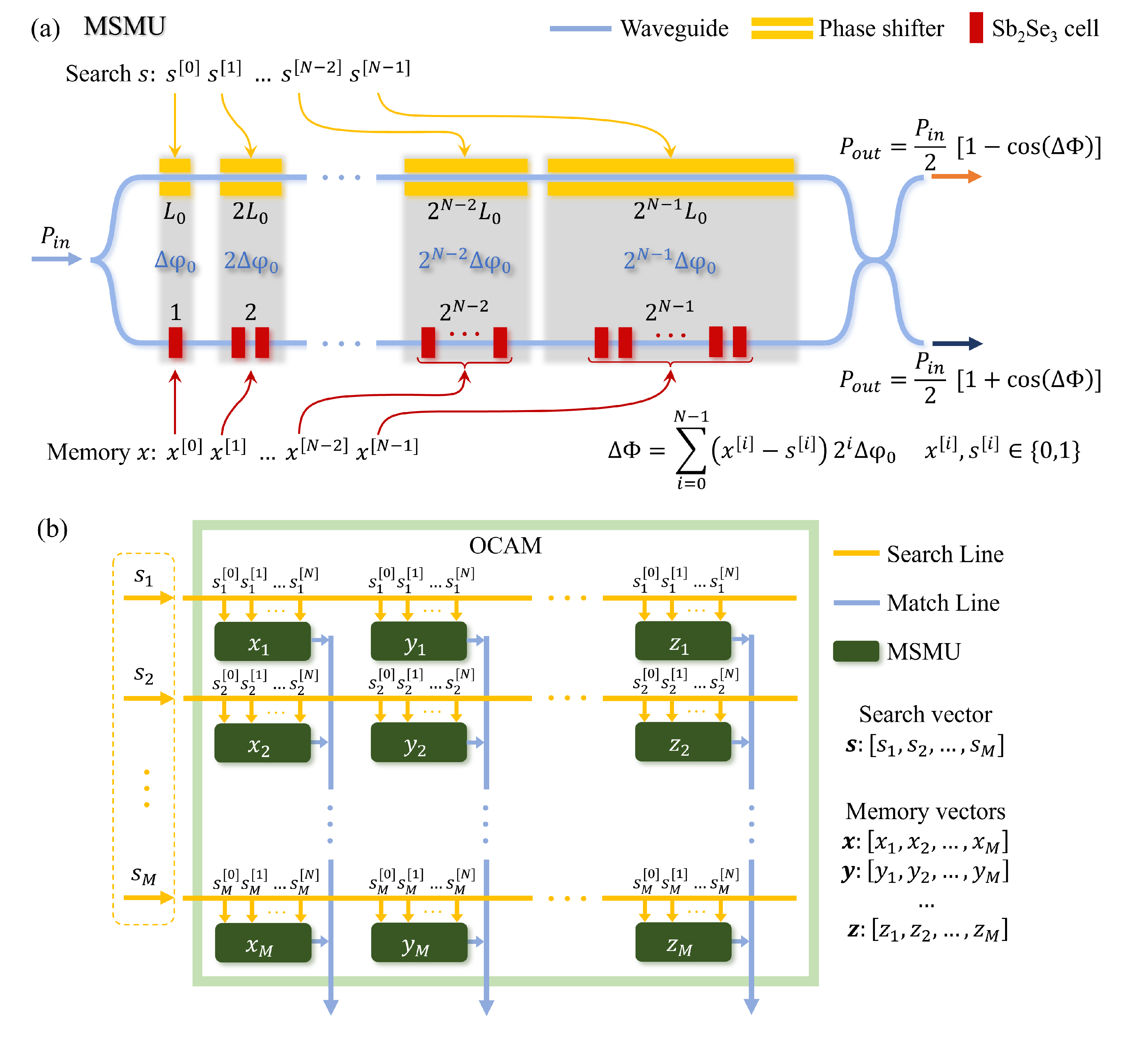
Figure 2.
(a) Schematic diagram of bit-widths, output optical power levels, and performance characteristics under different working segment configurations, (b) The configurations and output functions for performing scalar search and vector search respectively under different bit-width modes.
Figure 2.
(a) Schematic diagram of bit-widths, output optical power levels, and performance characteristics under different working segment configurations, (b) The configurations and output functions for performing scalar search and vector search respectively under different bit-width modes.
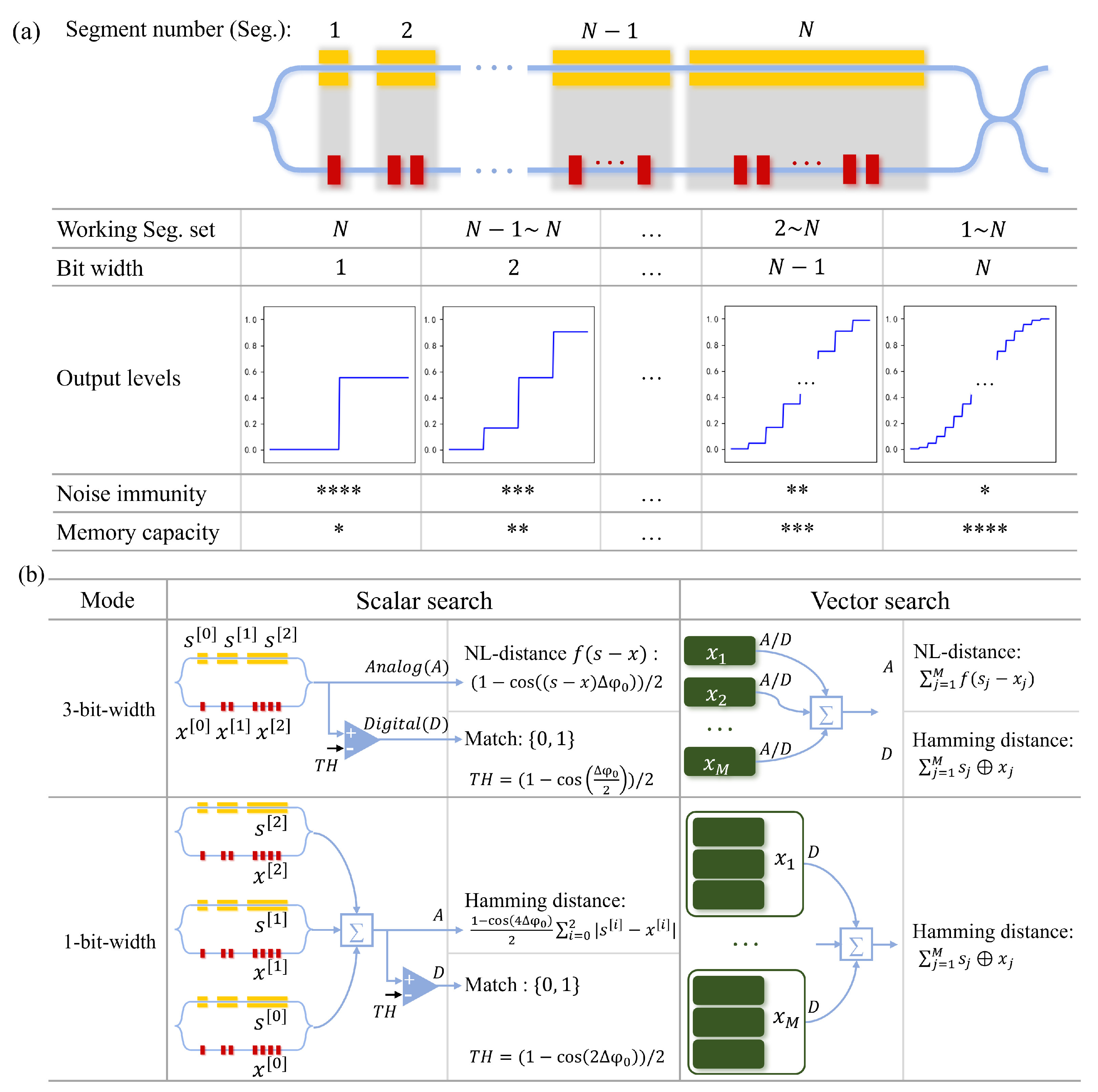
Figure 3.
(a) Fabrication structure, (b) SEM images of MMI and oxide window, (c) Experimental setup: multi-channel laser, optical power meter and the spatial light focusing system.
Figure 3.
(a) Fabrication structure, (b) SEM images of MMI and oxide window, (c) Experimental setup: multi-channel laser, optical power meter and the spatial light focusing system.
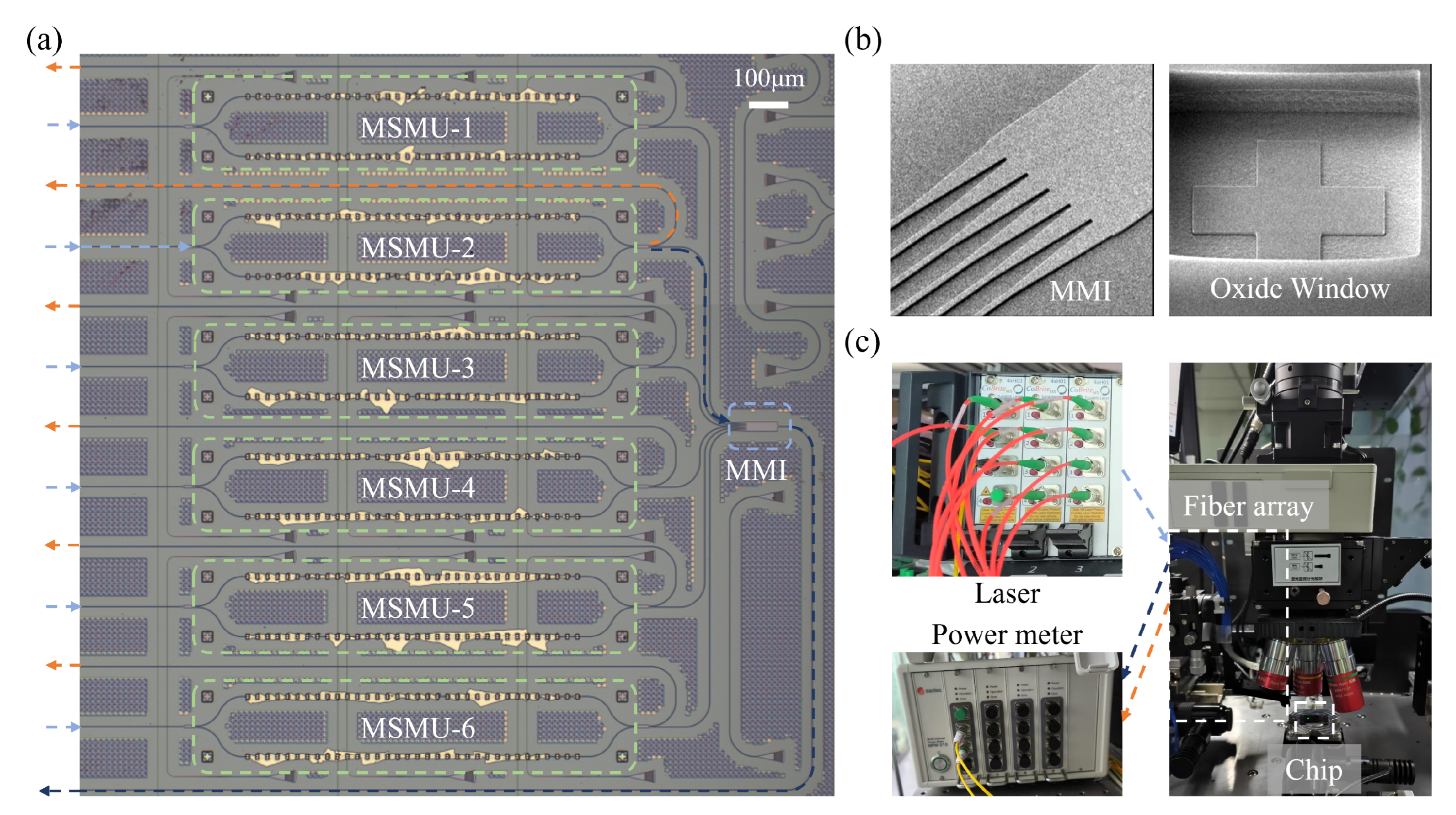
Figure 4.
Experimental results of MSMU: (a) Phase tuning characteristics of Sb2Se3 cells, (b) Statistical results of the phase shifts of Sb2Se3 cells (c) Output power levels under different bit-widths and stored data, and (c) Search results with different stored data under 3-bit-width.
Figure 4.
Experimental results of MSMU: (a) Phase tuning characteristics of Sb2Se3 cells, (b) Statistical results of the phase shifts of Sb2Se3 cells (c) Output power levels under different bit-widths and stored data, and (c) Search results with different stored data under 3-bit-width.
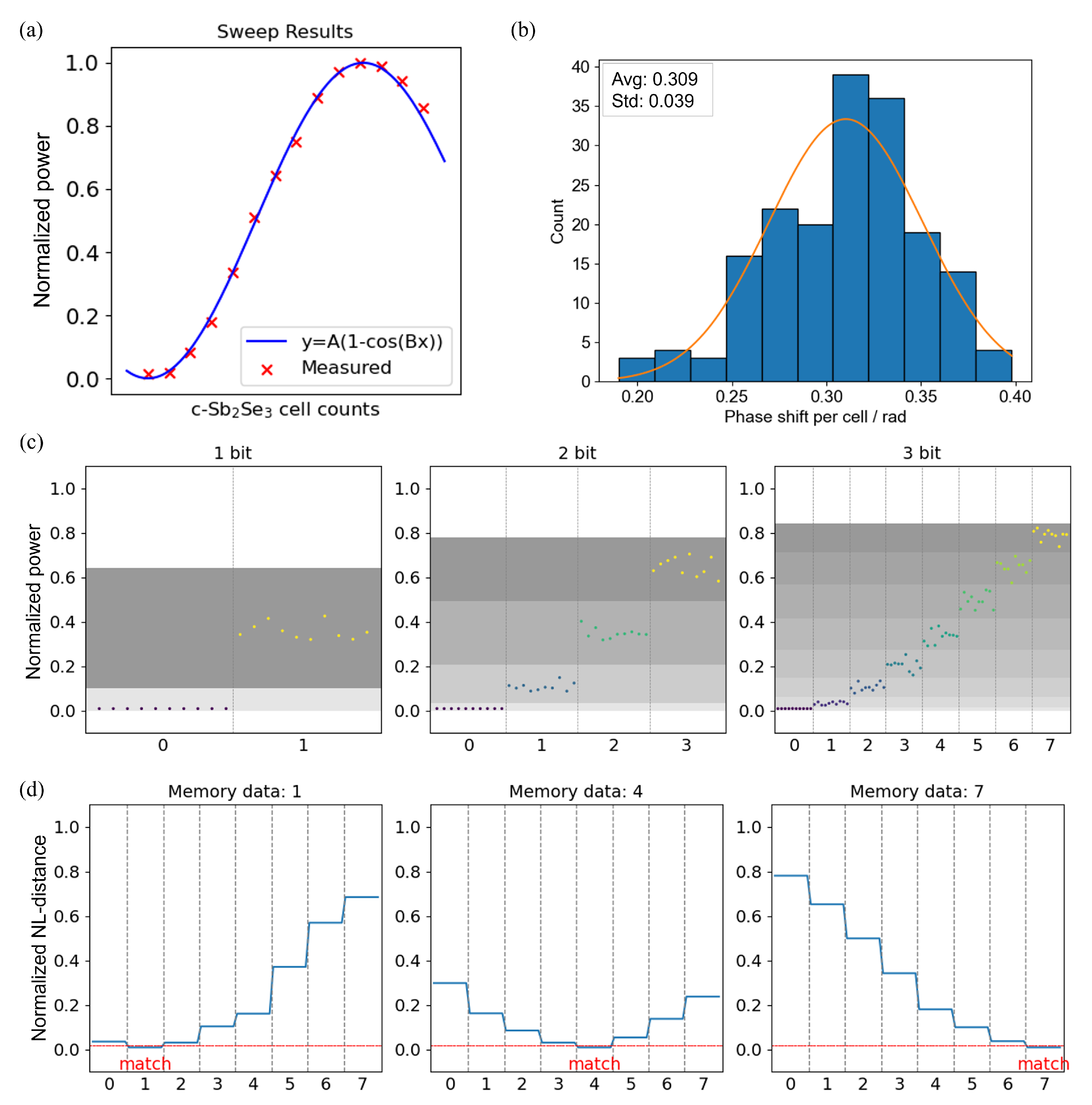
Figure 5.
(a) Schematic diagram of data preprocessing and kNN classification, (b-d) Accuracy of various distance calculation methods on the iris, wine, and breast cancer datasets at the optimal k. Simulation: bw, bit-width; HD, Hamming distance; NL: NL-distance; Benchmark: Manhattan, Euclidean and Hamming distance.
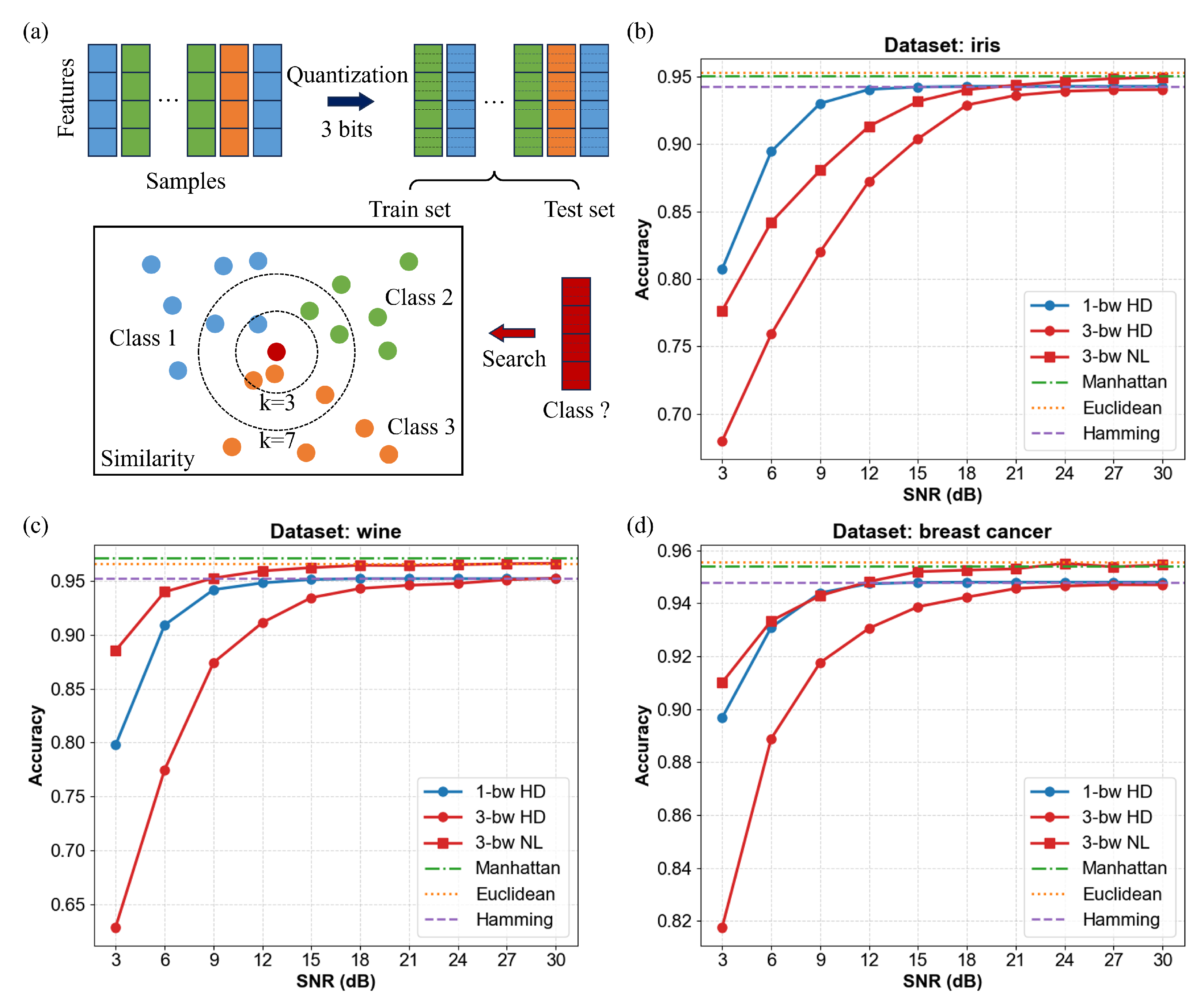
Figure 6.
Energy estimation of different bit-widths N.
Disclaimer/Publisher’s Note: The statements, opinions and data contained in all publications are solely those of the individual author(s) and contributor(s) and not of MDPI and/or the editor(s). MDPI and/or the editor(s) disclaim responsibility for any injury to people or property resulting from any ideas, methods, instructions or products referred to in the content. |
© 2026 by the authors. Licensee MDPI, Basel, Switzerland. This article is an open access article distributed under the terms and conditions of the Creative Commons Attribution (CC BY) license (http://creativecommons.org/licenses/by/4.0/).
Copyright: This open access article is published under a Creative Commons CC BY 4.0 license, which permit the free download, distribution, and reuse, provided that the author and preprint are cited in any reuse.


