Submitted:
27 January 2026
Posted:
28 January 2026
You are already at the latest version
Abstract
Directly modulated VCSEL transmitters are widely deployed in short-reach optical interconnects, yet further scaling of per-lane symbol rates in AI/HPC datacenter fabrics demands modulation beyond the practical limits of direct current modulation. We demonstrate a laterally integrated VCSEL–electro-absorption modulator (EAM) transmitter enabled by resonance-detuned coupling on an oxide-confined half-VCSEL platform. A localized 20 nm surface etch produces >5 nm resonance detuning, confirmed by measured spectra and supported by transfer-matrix and mode-matching simulations, which indicate strong slow-light-assisted lateral coupling into the modulator. Experimentally, the measured spectra confirm an 5 nm resonance separation. Static characterization shows a coupling ratio of 63% extracted from near-field profiles and an extinction ratio of 4 dB (based on modulator-side power) under a −2 V modulator bias, with an apparent 1 mW absorption at a 6 mA VCSEL drive current. Dynamic measurements demonstrate a small-signal 3-dB bandwidth of approximately 23 GHz and clear NRZ eye openings at 25 Gb/s and 30 Gb/s. These results validate resonance-detuned lateral integration as a compact and manufacturable approach to VCSEL-based externally modulated transmitters for next-generation short-reach interconnects.
Keywords:
VCSELs
; electro-absorption modulator
; lateral integration
; slow-light coupling
1. Introduction
Directly modulated vertical-cavity surface-emitting lasers (VCSELs) constitute the backbone of modern short-reach optical interconnects—particularly in data centers and high-performance computing clusters—owing to their high power efficiency, circular beam profile, wafer-scale manufacturability, and favorable cost structure for massive parallelism [1,2,3,4]. However, the next generation of intra-datacenter fabrics—driven by the rapid bandwidth scaling of AI/HPC clusters—demands higher per-lane symbol rates while simultaneously imposing stricter constraints on energy efficiency, thermal budgets, and link margins [5,6]. This creates an urgent imperative to extend the modulation bandwidth of VCSELs beyond their physical modulation limits [7,8]. Our group has previously demonstrated that transverse coupled cavity VCSELs (TCC-VCSELs) can effectively leverage the photon-photon resonance (PPR) effect to significantly enhance direct modulation bandwidth [9,10,11]. On the other hand, external or hybrid modulation has been widely explored. Silicon photonics modulators (rings and Mach–Zehnders) [12] and thin-film lithium niobate platforms [13] offer high bandwidth and good linearity, but typically rely on a separate CW laser, low-loss coupling, and tight thermal control [14,15,16]. Even with hybrid-integrated sources, these solutions increase packaging and alignment complexity compared with monolithic VCSEL transmitters [17,18], preserving the appeal of VCSEL-based links for cost-sensitive short-reach interconnects.
Building on these considerations, monolithically integrated VCSEL–electro-absorption modulator (EAM) transmitters have attracted strong interest as a route to combine VCSEL-class manufacturability with compact, low-voltage, high-speed electro-optic modulation. Vertically integrated EAM-VCSELs have reported 30-GHz optical bandwidth underscoring the feasibility of VCSEL-based externally modulated lasers for short-reach links [19]. However, because the modulator and laser cavities are optically coupled in the surface-normal direction, residual cavity coupling/feedback and the associated coupled-resonator dynamics can produce pronounced resonance features (response peaking) and sensitivity to detuning [20,21]. An alternative route is lateral integration, where the VCSEL couples into an in-plane waveguide section incorporating an EAM [22,23]. However, a key limitation of the lateral scheme is the difficulty of engineering strong, efficient coupling. Extracting sufficient optical power from the VCSEL into an in-plane modulator remains challenging. In this paper, we present a laterally integrated VCSEL-modulator platform featuring an in-plane, resonance-detuned coupling design. Compared with our previous approach, where coupling was induced by an effective-index difference via unequal oxide-aperture widths in the two cavities [23,24], the proposed structure achieves a substantially larger resonance detuning (>5 nm). This enlarged detuning stabilizes the coupling efficiency and enables efficient power transfer. Experimentally, we obtain 1 mW coupled optical power delivered to the modulator, together with a small-signal 3-dB modulation bandwidth exceeding 20 GHz and clear 25 Gb/s NRZ eye opening.
2. Strcuture and Modelling
The schematic of the proposed laterally integrated VCSEL–modulator device is shown in Figure 1(a). The device is fabricated on an oxide-confined VCSEL epitaxial platform and adopts a half-VCSEL configuration in which the epitaxial top distributed Bragg reflector (DBR) is intentionally limited to five mirror pairs. The vertical stack comprises a bottom epitaxial DBR, an multi-quantum-wells (MQWs) active region, an oxidation layer for current and optical confinement, and the reduced top epitaxial DBR. Limiting the top DBR to only five pairs enhances the sensitivity of the cavity resonance to surface perturbations, providing an effective handle for resonance engineering in the lateral integration scheme. A localized surface-etch region is introduced on the VCSEL side to deliberately shift the cavity resonance relative to the neighboring modulator section, thereby establishing an in-plane resonance detuning. With this resonance detuning, the VCSEL couples laterally into the slow-light mode [25,26] supported by the Bragg-reflector waveguide, enabling enhanced in-plane energy transfer. The modulator shares the MQWs stack but is defined by ion implantation, which forms a high-resistivity region to suppress lateral current spreading [27,28] and enables independent electrical biasing of the laser and modulator. To provide sufficient reflectivity for lasing, additional dielectric DBR stacks are deposited on the surface and designed for the operating wavelength band. Figure 1(b) shows a top view of the fabricated device. The VCSEL section is confined by a 5 µm x 5 µm oxide aperture, while the EAM section employs a 5 µm x 50 µm oxide aperture to form an extended electro-absorption interaction region. Separate metal electrodes are patterned to provide independent electrical access for VCSEL biasing and high-speed modulation driving.
Figure 2 presents the simulated resonance detuning and the resulting lateral coupling behavior. In Figure 2(a), the resonance spectra of the laser and modulator sections are calculated using the transfer-matrix method (TMM) [29,30]. Because the device adopts a half-VCSEL configuration with a reduced epitaxial top DBR, the cavity resonance is highly sensitive to changes in the surface optical thickness. Introducing a 20-nm surface etch in the laser section effectively reduces the optical cavity length, producing a clear blue-shift of the laser resonance. The calculation indicates that this etch depth yields a resonance separation of approximately 5 nm between the laser and modulator sections. Figure 2(b) shows the optical field distribution computed with a film mode-matching method using a commercial electromagnetic solver. The simulation reveals that, when the resonance detuning is present, the optical energy generated in the laser section couples efficiently into the laterally propagating in-plane mode supported by the modulator region, as evidenced by the strong forward-propagating field in the modulator section. Physically, the detuning promotes coupling of the laser emission into a highly dispersive slow-light lateral mode, which increases the effective interaction time and strengthens the coupling efficiency.
3. Experimental Results and Discussions
Figure 3 summarizes the experimental verification of the resonance-detuned coupling concept. Figure 3(a) shows the measured optical spectra collected from the two sections. Two distinct spectral bands are observed, separated by approximately 5 nm, which is in good agreement with the TMM prediction in Figure 2(a) for a 20-nm surface etch. The clear spectral separation confirms that the laser and modulator sections operate with intentionally detuned resonances, consistent with the design objective of promoting directional lateral coupling under detuned operation. Figure 3(b) shows the measured L–I characteristics, which reflect the overall optical power evolution as the VCSEL injection is increased. Stable lasing is obtained and the output power increases monotonically above threshold.The blue curve corresponds to the case where the VCSEL is forward biased while the modulator is left unbiased, yielding a maximum detected power exceeding 2.5 mW. The orange curve shows the result when the modulator is reverse biased at −2 V. A clear reduction in the detected output is observed, and the maximum power difference between the two curves reaches ~1 mW at a VCSEL drive current of 6 mA, indicating that approximately 1 mW of optical power is absorbed in the modulator under electro-absorption operation. We note that the photodetector measurement unavoidably includes the total optical power and cannot isolate the in-plane coupled output from the directly emitted VCSEL light. Therefore, the extracted absorption and modulation-induced power change should be interpreted as an apparent value, rather than the absolute coupled power delivered solely to the EAM section.
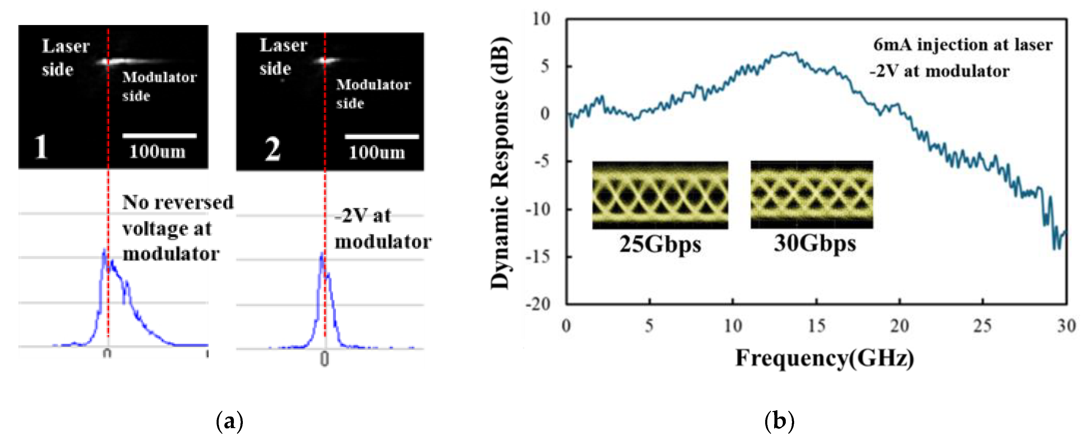
Figure 4 summarizes the measured static coupling behavior and the high-speed modulation performance of the laterally integrated VCSEL–EAM device. To visualize the in-plane power transfer, we first recorded the near-field emission distribution across the laser–modulator boundary. As shown in Figure 4(a1), when the device is operated under the designed resonance-detuned condition, the emission profile becomes clearly asymmetric with a intensity extension toward the modulator side. The corresponding lateral line profile confirms that a substantial fraction of optical power is transferred into the modulator region rather than remaining localized within the laser section, providing direct experimental evidence of detuning-enabled lateral coupling. By integrating the intensity on each side, we extract a coupling ratio of 63%, where the coupling ratio is defined as the modulator-side power divided by the total power collected from both sides. Static electro-absorption modulation is evaluated using the modulator-side output power as shown in Figure 4(a2). When the modulator is biased at −2 V, the modulator-side power decreases, yielding an extinction ratio of approximately 4 dB, where the extinction ratio is defined here based on the modulator-side power only. The dynamic performance is shown in Figure 4(b). A multimode fiber (MMF) is positioned above the modulator section to collect the modulated output, and the measured small-signal 3-dB bandwidth is approximately 23 GHz. Further optimization will focus on extending the usable bandwidth beyond 23 GHz by reducing parasitics, including lowering the device and pad capacitance, shortening the active/interconnect lengths, minimizing series resistance, and etc. Clear NRZ eye openings are obtained at 25 Gb/s and 30 Gb/s, while operation beyond 30 Gb/s becomes limited. This behavior correlates with the pronounced peaking (>5 dB) in the small-signal response. The peaking is mainly attributed to residual optical feedback (back-coupling) from the modulator side to the laser side. While wavelength detuning favors forward coupling, it does not fully eliminate reflections and coupled-cavity interactions in the present device. In addition, the MMF inevitably collects part of the light emitted from the laser side, so the detected waveform cannot be purely attributed to the modulator-side output in the current measurement configuration. Further optimization will target suppressing laser-side emission and reducing feedback-induced peaking. Selectively adding extra dielectric DBR pairs on the laser side can increase top reflectivity and minimize surface output, directing more power into the in-plane path. In parallel, refining the coupling interface/boundary conditions and introducing absorbing regions (lossy terminations) can suppress back-coupling from the modulator to the laser and flatten the frequency response.
4. Conclusions
In conclusion, we demonstrate a laterally integrated VCSEL–EAM transmitter enabled by resonance-detuned coupling on a half-VCSEL platform. A localized 20-nm surface etch produces a detuning >5 nm, as confirmed by spectra and consistent with simulations, and drives slow-light-assisted lateral power transfer into the modulator. Experimentally, the device shows strong coupling (63% coupling ratio), ~4 dB static extinction ratio , and an apparent 1 mW absorption power. High-speed measurements yield a 23 GHz small-signal 3-dB bandwidth and clear NRZ eye openings until 30 Gbps. Future work will focus on flattening the frequency response and further extending the usable modulation bandwidth through parasitic reduction, as well as suppressing laser-side emission and feedback.Overall, the demonstrated resonance-detuned lateral integration provides a practical pathway toward compact, manufacturable VCSEL-based externally modulated transmitters for next-generation short-reach optical interconnects.
Author Contributions
Conceptualization, S.H.; Data curation, S.H. and X.Z.; Funding acquisition, S.H.; Investigation, X.Z., B.T. and L.Z.; Methodology, S.H.; Project administration, S.H. and B.L.; Software, S.H. and X.Z.; Supervision, S.H. and B.L.; Writing—original draft, S.H. ; Writing—review and editing, X.Z., B.T. and L.Z. All authors have read and agreed to the published version of the manuscript.
Funding
This work is supported by National Natural Science Foundation of China (62205026) and National Key Research and Development Program of China (2023YFB2905500).
Data Availability Statement
The data underlying the results presented in this paper are not publicly available at this time but may be obtained from the authors upon reasonable request.
Conflicts of Interest
The authors declare no conflicts of interest.
References
- Koyama, F. Recent advances of VCSEL photonics. J. Lightwave Technol. 2007, 24(12), 4502–4513.
- Iga, K. VCSEL: born small and grown big. Proc. SPIE 2020, 11263, 1126302.
- Ledentsov, N. N.; Makarov, O. Y.; Shchukin, V. A.; Kalosha, V. P.; Ledentsov, N.; Chrochos, L.; Sanayeh, M. B.; Turkiewicz, J. P. High speed VCSEL technology and applications. J. Lightwave Technol. 2022, 40(6), 1749–1763.
- Hu, S.; Zhang, X.; Li, C.; Yin, H.; Li, X.; Xin, X. Latest advances in VCSEL technology for next-generation data center network. Chin. Opt. Lett. 2024, 22(11), 111401.
- Maniotis, P.; Kuchta, D. M. Exploring the benefits of using co-packaged optics in data center and AI supercomputer networks: a simulation-based analysis. J. Opt. Commun. Netw. 2024, 16, A143–A156.
- Xie, C.; Zhang, B. Scaling optical interconnects for hyperscale data center networks. Proceedings of the IEEE, 2022, 110(11), 1699-1713.
- Cheng, H.T.; Yang, Y.C.; Liu, T.H.; Wu, C.H. Recent advances in 850 nm VCSELs for high-speed interconnects. Photonics 2022, 9(2), 107.
- Pan, G.; Xun, M.; Zhou, X.; Sun, Y.; Dong, Y.; Wu, D. Harnessing the capabilities of VCSELs: unlocking the potential for advanced integrated photonic devices and systems. Light Sci. Appl. 2024, 13(1), 229.
- Hu, S.; Ahmed, M.; Bakry, A.; Koyama, F. Low chirp and high-speed operation of transverse coupled cavity VCSEL. Jpn. J. Appl. Phys. 2015, 54(9), 090304.
- Hu, S.; Koyama, F. Coupled mode analysis of high-speed transverse coupled cavity vertical-cavity surface-emitting laser for low frequency chirp operations. IEICE Electron. Express 2021, 18(13), 20210239.
- Hu, S.; Gu, X.; Ibrahim, H.R.; Nakahama, M.; Shinada, S.; Koyama, F. 1060-nm single-mode transverse coupled cavity VCSEL with intra-cavity surface relief for 58-Gbps modulation and 5-km single-mode fiber transmission. Appl. Phys. Lett. 2022, 120(26),261110.
- Shi, Y.; Zhang, Y.; Wan, Y.; Yu, Y.; Zhang, Y.; Hu, X.; Xiao, X.; Xu, H.; Zhang, L.; Pan, B. Silicon photonics for high-capacity data communications. Photonics Res. 2022, 10(9), A106–A134.
- Weigel, P. O.; Zhao, J.; Fang, K.; Al-Rubaye, H.; Trotter, D.; Hood, D.; Mudrick, J.; Dallo, C.; Pomerene, A. T.; Starbuck, A. L.; DeRose, C. T.; Lentine, A. L.; Rebeiz, G.; Mookherjea, S. Bonded thin film lithium niobate modulator on a silicon photonics platform exceeding 100 GHz 3-dB electrical modulation bandwidth. Opt. Express 2018, 26(18), 23728–23739.
- Dourado, D. M.; de Farias, G. B.; Gounella, R. H.; Rocha, M. de L.; Carmo, J. P. Challenges in silicon photonics modulators for data center interconnect applications. Opt. Laser Technol. 2021, 142, 107376.
- Yoo, S.; Park, H.; Lee, J. C.; Kang, E. K.; Huh, J. Y.; Cho, G. S.; Kang, H.; Moon, D. W.; Lee, J. J.; Lee, J. K. 53 GBd PAM-4 fully-integrated silicon photonics transmitter with a hybrid flip-chip bonded laser. Opt. Express 2022, 30(23), 41980–41994.
- Padmaraju, K.; Bergman, K. Resolving the thermal challenges for silicon microring resonator devices. Nanophotonics 2014, 3(4), 269-281.
- Marchetti, R.; Lacava, C.; Carroll, L.; Gradkowski, K.; Minzioni, P. Coupling strategies for silicon photonics integrated chips. Photonics Res. 2019, 7(2), 201-239.
- Ranno, L.; Gupta, P.; Gradkowski, K.; Bernson, R.; Weninger, D. Integrated photonics packaging: challenges and opportunities. ACS Photonics 2022, 9(11), 3467-3485.
- Marigo-Lombart, L.; Rumeau, A.; Viallon, C.; Arnoult, A.; Calvez, S.; Monmayrant, A.; Gauthier-Lafaye, O.; Rosales, R.; Lott, J. A.; Thienpont, H. High frequency operation of an integrated electro-absorption modulator onto a vertical-cavity surface-emitting laser. J. Phys.: Photonics 2019, 1, 02LT01.
- Van Eisden, J.; Yakimov, M.; Tokranov, V.; Varanasi, M.; Mohammed, E. M.; Young, I. A.; Oktyabrsky, S. Optically decoupled loss modulation in a duo-cavity VCSEL. IEEE Photonics Technol. Lett. 2008, 20, 42–44.
- Yakimov, M.; Van Eisden, J.; Tokranov, V.; Varanasi, M.; Oktyabrsky, S.; Mohammed, E. M.; Young, I. A. Concept of feedback-free high-frequency loss modulation in detuned duo-cavity VCSEL. J. Vac. Sci. Technol. B 2010, 28, C3G32–C3G37.
- Shimada, T.; Matsutani, A.; Koyama, F. Lateral integration of VCSEL and slow light Bragg reflector waveguide devices. Appl. Opt. 2014, 53, 1766–1774.
- Dalir, H.; Matsutani, A.; Koyama, F. Low-voltage, high-speed and compact electro-absorption modulator laterally integrated with 980-nm VCSEL. Opt. Express 2014, 22, 25746–25755.
- Hu, S.; Ahmed, M.; Bakry, A.; Koyama, F. Low chirp and high-speed operation of transverse coupled cavity VCSEL. Jpn. J. Appl. Phys. 2015, 54(9), 090304.
- Gu, X.; Shimada, T.; Imamura, T.; Matsutani, A.; Koyama, F. Beam steering in GaInAs/GaAs slow-light Bragg reflector waveguide amplifier. Appl. Phys. Lett. 2011, 99, 211107.
- Shimada, T.; Matsutani, A.; Koyama, F. Compact slow-light electro-absorption modulator laterally integrated with 980 nm vertical-cavity surface-emitting laser. Appl. Phys. Express 2013, 6(12), 122102.
- Walker, J. D.; Kuchta, D. M.; Smith, J. S. Vertical-cavity surface-emitting laser diodes fabricated by phase-locked epitaxy. Appl. Phys. Lett. 1991, 59, 2079–2081.
- Sysak, M. N.; Anthes, J. O.; Bowers, J. E.; Raday, O.; Jones, R. Integration of hybrid silicon lasers and electroabsorption modulators. Opt. Express 2008, 16(17), 12478–12486.
- Kalusniak, S.; Sadofev, S.; Halm, S.; Henneberger, F. Vertical cavity surface emitting laser action of an all monolithic ZnO-based microcavity. Appl. Phys. Lett. 2011, 98, 011101.
- Yu, S. F. An improved time-domain traveling-wave model for vertical-cavity surface-emitting lasers. IEEE J. Quantum Electron. 1998, 34(10), 1938–1948.
Figure 1.
(a) Schematic picture of the proposed laterally integrated VCSEL–modulator ; (b) Top view of the fabricated device.
Figure 1.
(a) Schematic picture of the proposed laterally integrated VCSEL–modulator ; (b) Top view of the fabricated device.
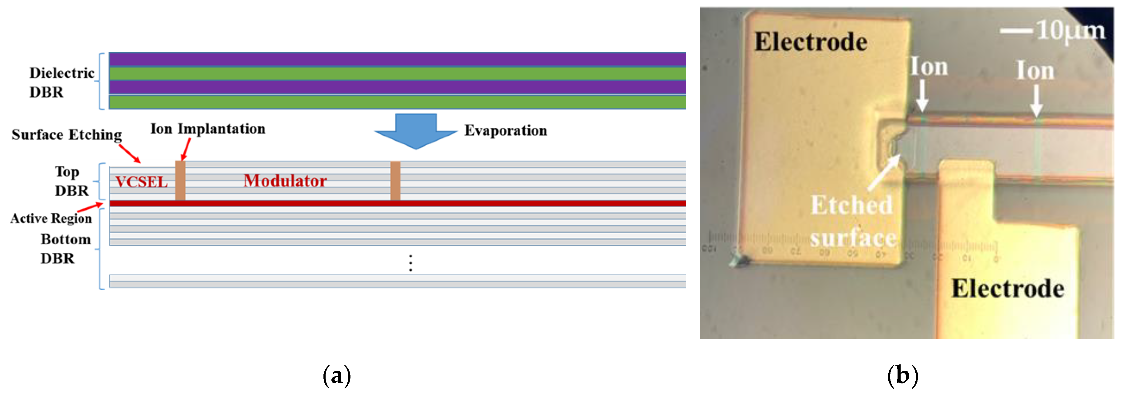
Figure 2.
(a) Calculated resonance spectra of the laser and modulator sections (b) Optical field distribution simulated by a film mode-matching method.
Figure 2.
(a) Calculated resonance spectra of the laser and modulator sections (b) Optical field distribution simulated by a film mode-matching method.
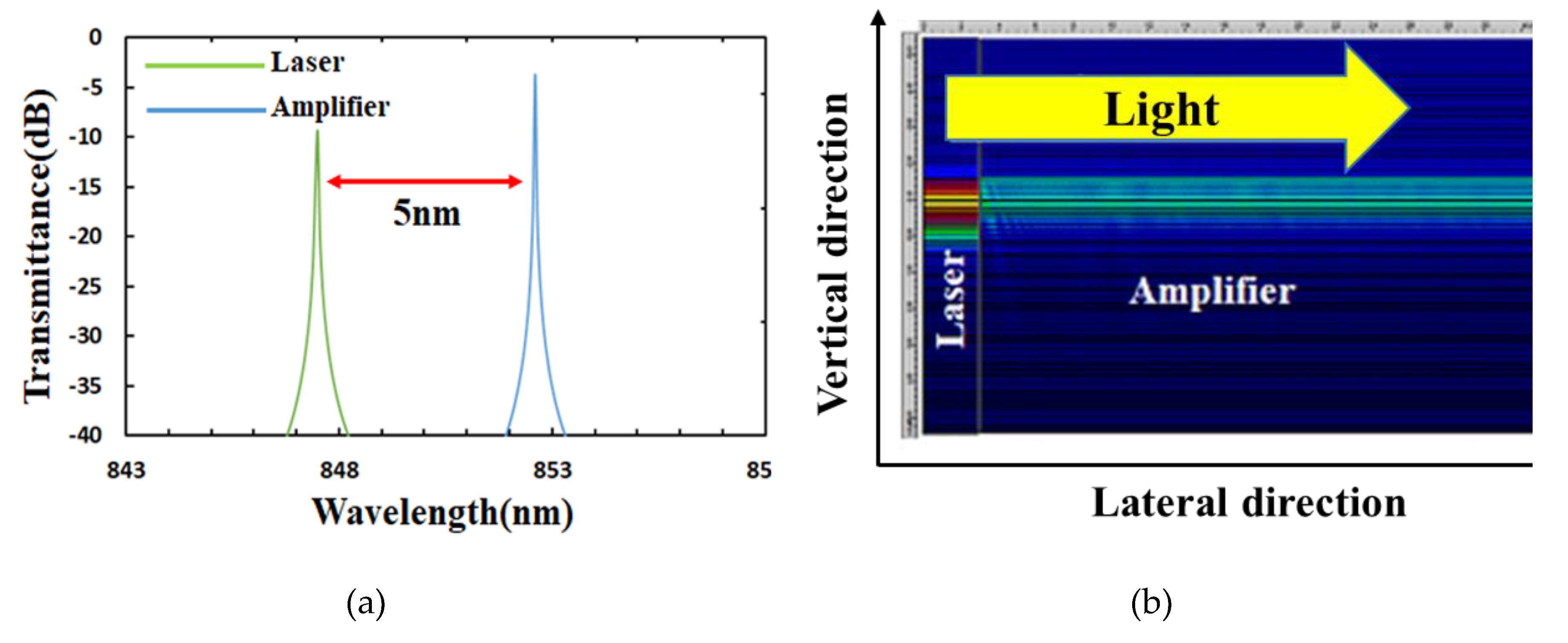
Figure 3.
(a) Measured emission spectra confirming an approximately 5 nm wavelength separation between the laser and modulator resonances; (b) L–I characteristics measured with the modulator unbiased (blue) and reverse biased at −2 V (orange).
Figure 3.
(a) Measured emission spectra confirming an approximately 5 nm wavelength separation between the laser and modulator resonances; (b) L–I characteristics measured with the modulator unbiased (blue) and reverse biased at −2 V (orange).
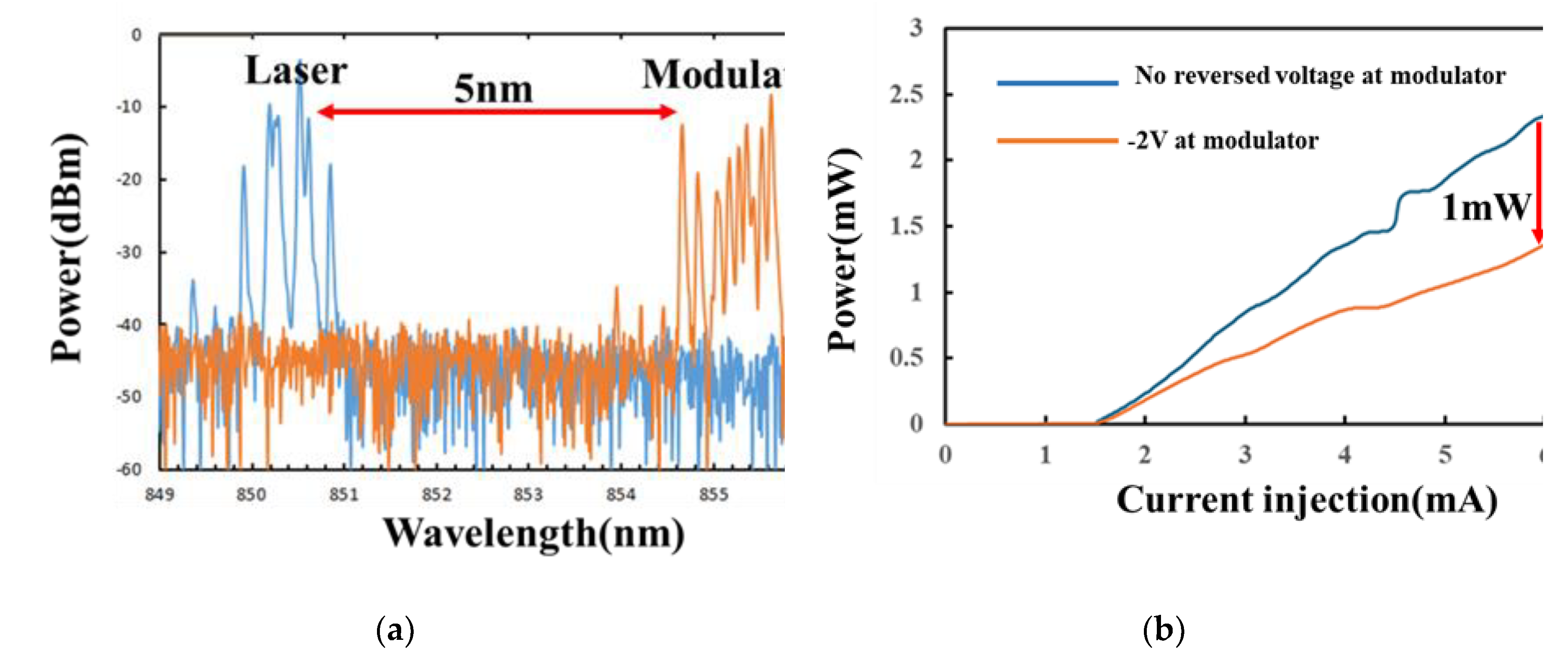
Figure 4.
(a) Near-field emission images and corresponding lateral line profiles with the modulator unbiased and at −2 V; (b) Small-signal E/O frequency response and NRZ eye diagrams at 25 and 30 Gb/s.
Figure 4.
(a) Near-field emission images and corresponding lateral line profiles with the modulator unbiased and at −2 V; (b) Small-signal E/O frequency response and NRZ eye diagrams at 25 and 30 Gb/s.
Disclaimer/Publisher’s Note: The statements, opinions and data contained in all publications are solely those of the individual author(s) and contributor(s) and not of MDPI and/or the editor(s). MDPI and/or the editor(s) disclaim responsibility for any injury to people or property resulting from any ideas, methods, instructions or products referred to in the content. |
© 2026 by the authors. Licensee MDPI, Basel, Switzerland. This article is an open access article distributed under the terms and conditions of the Creative Commons Attribution (CC BY) license (http://creativecommons.org/licenses/by/4.0/).
Copyright: This open access article is published under a Creative Commons CC BY 4.0 license, which permit the free download, distribution, and reuse, provided that the author and preprint are cited in any reuse.


