Submitted:
26 January 2026
Posted:
28 January 2026
You are already at the latest version
Abstract
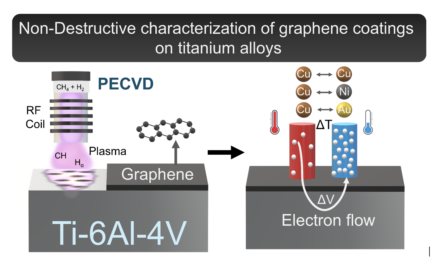
In this work the deposition of graphene coatings on substrates of an ELI grade Ti-6Al-4V alloy was carried out using the Plasma Enhanced Chemical Vapor Deposition (PECVD) technique. The purpose of this study was to improve the surface properties of the material. The characterization of the material was carried out by non-destructive techniques, such as Raman Spectroscopy and Thermoelectric Potential. A preliminary characterization of Ti substrates was carried out by Raman spectroscopy. Conversely, thermoelectric potential tests were conducted using three distinct tip systems and four different temperature gradients. Lastly, some surface roughness measurements were conducted on all samples, both coated and uncoated. Graphene micro-structured coatings were obtained using a plasma activated mixture of hydrogen and methane gases with equimolar feed ratio (1:1 H₂:CH₄) at a temperature of 850°C and a plasma exposure of 150 Watts and duration of 15 minutes. Raman spectra verified the presence of uniform micrometric graphene on the surface of Ti substrates. Graphene-coated Ti-6Al-4V ELI substrates exhibited absolute thermoelectric potentials between 1.9 and 3.4 μV/K, indicating metallic-like behavior and suitability for thermoelectric sensing. In the eddy current analyses, it was found that the 50 kHz frequency provided the highest sensitivity for differentiating between samples. An inverse relationship was identified between substrate thickness and phase angle, and a direct relationship with calculated electrical conductivity. This direct relation is attributed to penetration depth and interactions due to the chemical nature of the substrate and coating. Despite a slight increase in surface roughness after graphene deposition, values remained comparable to the base alloy, preserving compatibility for biomedical integration. The Au-Cu testing system demonstrated enhanced sensitivity to Seebeck coefficient variations, suggesting its promise for high-resolution thermal sensing. These results support potential applications in implantable or wearable temperature sensors, energy harvesting devices, and smart biomedical interfaces. The thickness of the graphene coating was also characterized by SEM, which showed that the films deposited by PECVD are about 1 micron thick.
Keywords:
plasma enhanced CVD (PECVD)
; micron-sized graphene coatings
; thermoelectric Power
; Ti-6Al-4V ELI GRADE
1. Introduction
Titanium alloys are frequently utilized as biomaterials due to their mechanical properties and exceptional corrosion resistance[1,2].
Ti-6Al-4V is the most prevalent titanium alloy. The alloy’s combination of α and β phases endows it with fatigue resistance and ductility. The ELI grade of this alloy is defined as “extra low interstitials,” which refers to the presence of interstitial atoms, such as Fe, O, N, and H, within its lattice. This composition enhances the alloy’s fracture tenacity[3,4,5].
Several authors [6,7,8] have studied the effects of various mechanical and chemical factors on the surface of this alloy to improve its performance as a biomaterial. These factors include corrosion resistance and improved morphology to promote cell growth and adhesion to bones and other tissues.
However, the wear and corrosion resistance of Ti-6Al-4V ELI alloy as a biomaterial are still under study, mainly because its practical use involves constant stress and continuous exposure to body fluids rich in ions that induce corrosion.
The use of coatings has emerged as a solution to the aforementioned drawbacks. These coatings are designed to protect the substrate from various phenomena, including mechanical wear, oxidation, and corrosion, among others[9,10,11].
A variety of techniques have been developed for the purpose of generating these coatings. The selection of the technique to employ is contingent upon the type of substrate (i.e., polymers, ceramics, metal alloys, or composite materials). Similarly, each technique possesses its own set of advantages and limitations in terms of the process that must be followed to synthesize and deposit the coating material.
The chemical vapor deposition (CVD) technique is widely used and well established. It is comprised of a precursor gas that flows into a closed chamber. In this environment, the substrate is heated, and the deposition of the coatings occurs as a result of the pyrolysis reaction of the precursor in the gas phase. Plasma-enhanced chemical vapor deposition (PECVD) while it shares the similarity of feeding the precursors in the gas phase, the salient difference is the use of an electric source required to create a rich chemistry environment by collision of neutrals with electrons. This rich chemical environment contains electrons, ions, radicals and vibrational excited species. Furthermore, a pressure reduction system is necessary to stably maintain a homogenized plasma reactive environment[12,13,14].
PECVD is a process that facilitates the deposition of a diverse array of chemical species that are hard to dissociate. Moreover, PECVD offers the advantage to occur at lower temperature and faster deposition times compared with conventional thermal methods[15,16]. Among the coatings applied to metallic substrates, graphene has emerged as a particularly salient option due to its unique physical and chemical properties, as well as its ease of synthesis. This process does not involve the use of costly or sophisticated precursors, making it a cost-effective solution[17,18].
Thin-film graphene deposition onto a variety of substrates has been in the limelight in recent years due to its robustness and outstanding properties. For instance, by leveraging graphene’s excellent electrical conductivity and mechanical flexibility, research community have demonstrated implantable and wearable temperature sensors capable of monitoring physiological parameters with high sensitivity and rapid response times[19,20]. Similarly, graphene-coated electrodes and membranes have been merged into energy harvesting systems such as piezoelectric generators to efficiently convert thermal variations into usable electrical power[21,22]. In the biomedical sector, these same deposition techniques have given rise to smart interfaces that impeccably integrate with tissue, enabling real-time tracking of biochemical signals[23,24,25,26]. Beyond sensing and harvesting, thin graphene films have also been explored to enhance the performance and longevity of energy-storage devices: their high surface area and conductivity improve charge-discharge rates in batteries and supercapacitors[27,28,29]. Finally, when applied as ultra-thin protective coatings, graphene offers exceptional resistance to corrosion, protecting metal surfaces in harsh environments without sacrificing weight or thickness[30].
This technique has been studied for the growth of coatings of different chemical species on Ti-6Al-4V substrates to improve properties such as corrosion resistance. Such is the case of Oliveira et al. [31]who used plasma-assisted CVD to coat this alloy with nitride films. They achieved higher impedance values with these different nitride systems than with the base material.
Similarly, Cho et al. [32]used PECVD to deposit amorphous carbon coatings on Ti-6Al-4V. These coatings allowed for corrosion rates 30 times lower than the bare alloy and exhibited improved biocompatibility during in vitro tests with cell cultures.
It has been demonstrated that graphene exhibits high thermal (above 3000 W/m⋅K) and electron mobility (2.5x105 cm2/V⋅s), as well as superb mechanical strength (Young’s modulus of 1 TPa and intrinsic strength of 130 GPa). This coating is also a highly suitable option for biomedical materials, such as the ELI grade Ti-6Al-4V alloy, due to its inherent properties, including chemical resistance, thermal stability, gas impermeability, and antibacterial potential[33,34,35,36,37].
Different authors, such as Wang et al.[38], have reported on the use of graphene as a coating for biomaterials. They used PECVD to deposit graphene on Ti-6Al-4V substrates and found that the behavior of different bacterial and fungal pathogens, such as P. gingivalis and C. albicans, changed when they came in contact with the alloy coated with graphene on its surface. These pathogens tended to deform and even shrink, a behavior which was not observed in the bare material by itself.
Romo-Rico et al. [39]also used PECVD to deposit graphene on a CoCr alloy, which is used as a biomaterial. They found that, in addition to promoting cell adhesion, this type of coating had an antibacterial effect against Staphylococcus aureus and Pseudomonas aeruginosa.
Similarly, Malhotra et al. [40]evaluated the corrosion resistance of a Ti-6Al-4V ELI system with nanostructured graphene coatings and found that the corrosion rate decreased by up to five times compared to the alloy without coatings in a 0.5 M NaCl environment with 2 ppm fluoride.
In terms of characterization, Raman spectroscopy has emerged as a pivotal technique for the analysis of carbon-based materials, including graphene.
This technique is considered as a rapid, non-destructive, and high-resolution way to characterize graphene. It is based on the effect of inelastic light scattering, otherwise known as “Raman scattering.” This phenomenon occurs when light interacts with the molecules of a material and scatters at different energy levels corresponding to the vibrational modes of the molecule[41,42].
Ferrari & Basko [43] detail the information that can be obtained from Raman spectra of graphene. They highlight the usefulness of the technique since it can determine the number and orientation of synthesized graphene layers, their quality, and the types of their edges. Most importantly, it provides knowledge about sp² carbon allotropes since they are the fundamental unit of graphene. Thus, these authors provide extensive information about the technique’s usefulness in determine graphene’s structure and chemical properties, as well as a scientifically rigorous approach to interpret results and the valuable information obtained from them, also highlighting the importance and usefulness of the Raman spectroscopy technique for the study of graphene.
Eckmann et al. [44]used Raman spectroscopy to analyze defects and disorder in graphene by examining the intensities of peaks in this material’s characteristic bands and the relationships between them. They associate the ratio of intensities in the D and D’ bands with defects related to vacancies and boundaries. For vacancies and boundaries, the presence of these defects is indicated by a decrease and a minimum in the ratio of intensities, respectively.
The non-destructive thermoelectric power technique (TEP) is predicated through the Seebeck effect, which establishes that if a thermal gradient is induced between a dissimilar junction, a potential voltage will be produced in the metallic sample that is integrated into such a dissimilar junction. This technique employs the thermoelectric potential of a material to characterize its conductive properties, as any defects or perturbations within the crystal lattice, such as elements in solid solution, precipitates, or dislocations, which can affect this potential. These defects contribute to changes in the material’s electrical and elastic properties, thereby inducing a variation in the thermoelectric potential[45,46].
Park et al. [47]reported using this non-destructive technique to evaluate the content of interstitial elements in steels, such as AISI 1090, as well as to analyze residual stresses in aluminum, nickel, and bronze alloys. In both cases, they report linear correlations with respect to the evaluation variables: % nitrogen for evaluating interstitial elements and stress values for analyzing residual stresses.
Carreón et al. [48,49]used the thermoelectric potential technique to analyze wear in Ti-6Al-4V alloys and evaluate aging and precipitation formation. This demonstrated the sensitivity of the technique to surface analysis of this class of materials.
Eddy currents, also known as Foucault currents, are a non-destructive inspection technique that uses a magnetic field generated by an electric current in a coil to detect surface and subsurface discontinuities.
The issue of conductivity changes in alloys, such as nickel-based superalloys and Ti-6Al-4V, continues to be studied. It appears that conductivity changes due to subtle microstructural changes, such as the transition from long-range to short-range order or changes in the numerical density and size of precipitates[50].
Eddy currents testing (ECT) involves the flow of an electric current through a circuit that operates the primary coil. However, all electric currents encounter resistance to their flow. In an alternating current system, this resistance is represented by impedance (Z), which is expressed as the sum of a real part (R) and an imaginary part (X). The real part is the common resistance, and the imaginary part is called reactance. There are two types of reactance: inductive (L) and capacitive (C), due to the presence of inductors and capacitors, respectively[51].
Rosen and Horowitz [52] identified a decrease in the conductivity of 2024 aluminum alloys during the alloys’ aging process at temperatures between 21 and 190 °C. This decrease is due to the formation of GP and GPB zones, also called Guinier-Preston and Guinier-Preston-Bagaryatsky zones. These zones form rapidly during tempering and are predominantly composed of solute elements. Essentially, they are tiny agglomerations of atoms that precipitate in the matrix during the initial stages of precipitation hardening. The kinetics of forming these zones are governed by the mobility of copper and magnesium atoms, as well as their interaction with vacancies. The formation of these solute atom agglomerations directly influences conductivity measurements in eddy current tests.
Surface roughness depends heavily on the manufacturing method used. This property enables us to understand how an object interacts with its environment, as it is directly related to phenomena such as friction, wear, and the adhesion of bodies to each other[53,54].
In the specific context of using Ti-6Al-4V ELI as a biomaterial, surface roughness is important because cells grow preferentially on rough surfaces. This affects the rate and quality of new tissue formation (Deligiani et al.[55]).
In this work, we report on our search for the optimal parameters for graphene deposition on Ti using PECVD, Raman spectroscopy characterization. Additionally, we studied the Seebeck coefficient of the graphene-coated Ti-6Al-4V ELI system using the cold-tip-hot-tip thermoelectric potential technique. Furthermore, we report the changes in surface roughness of this system after graphene is deposited on the Ti alloy substrate.
2. Materials and Methods
2.1. Materials
This investigation was carried out using three sets of samples of Ti-6Al-4V alloy ELI grade. Each set contained three samples with different thicknesses (1.6 mm, 3.2 mm, and 7 mm).
Furthermore, titanium substrates with a diameter of 15 millimeters and a thickness of 0.125 millimeters were employed in the preliminary tests to ascertain the optimal parameters for graphene growth by PECVD.
2.2. CVD & PECVD Preliminary Tests & Deposition on Ti-6Al-4V ELI Grade Samples
The samples were mirror polished with sandpaper meshes of 240, 600, they were sonicated in an acetone solution for 10 minutes to remove surface contamination. The samples were then oven-dried for 4 hours at 80 °C before being placed inside the reactor chamber, which was subsequently pumped to vacuum.
The experiments were conducted in an in-house-built plasma reactor (Figure 1)[56], maintaining a constant reaction pressure of 0.1 torr. For the preliminary study we conducted CVD and PECVD on small Titanium-substrates (15 mm diameter, 0.125 mm thickness). The Ti-substrate were heated in a tubular furnace at temperatures ranging from 425 to 850 °C, with a ramp rate of 10 °C min–1. A flow of 20 sccm was controlled via mass flow controller (MFC) with an equimolar mixture of methane and hydrogen. The samples were maintained at 850 °C for 2 hours, followed by plasma exposure between 15 and 30 minutes, respectively, at 150 W plasma power. The samples were then cooled to room temperature at a rate of 20 °C min–1. Based on the preliminary study results, the optimal parameters for graphene synthesis were applied to various sizes of Ti-6Al-4V with various thickness of 1.6 mm, 3.2 mm, and 7 mm.
2.3. Raman Characterization of Preliminary Ti Samples
The graphene films were characterized using a Horiba LabRAM HR Raman spectrometer. The system was equipped with an Olympus microscope and lenses and used a 632 nm laser with a collection time of 10 seconds at room temperature for the measurement.
2.4. TEP Characterization of Ti-6Al-4V ELI Grade Samples
The thermoelectric power measurements of the ELI grade Ti-6Al-4V samples, with the graphene coating already deposited, were obtained by employing a Thermo-Sorter apparatus manufactured by Walker Scientific, Inc. This equipment uses the hot tip technique (Figure 2), which involves the use of three different pairs of tips. The pair of tips employed were Cu-Cu, Cu-Ni & Cu-Au.
In addition to the three aforementioned systems, it is important to acknowledge that the measurements were obtained under varying thermal gradients (∆T = 50 °C, 40 °C, 30 °C, and 20 °C) for each pair of tips utilized. This procedure was repeated for all nine studied samples, with a total of 30 measurements being recorded for each sample.
It should be noted that the recorded measurements provide only µV values, that is to say, only voltage variations. To obtain the absolute value, also referred to as the Seebeck coefficient[45], it is necessary to refer to its formula described in Equation 1. [45]
S=∆V/∆T
The presented equation elucidates the phenomenon known as the Seebeck effect, which dictates that the generation of a thermal gradient within a system of differing composition will yield a voltage difference that can be quantitatively measured by means of a voltimeter[45]. Given that the measurements indicate the value of the voltage difference, it is important to determine the thermal gradient utilized to obtain the absolute potential. This is achieved by dividing the measured voltage value by the temperature difference, as the previous equation shows, thereby yielding the value of the Seebeck coefficient (S).
2.5. Conductivity Measurements Using Eddy Currents Testing (ECT)
The OLYMPUS NORTEC 500D was used to characterize Ti-6Al-4V grade ELI samples with graphene on their surface using the eddy current technique. Measurements were taken at various inspection frequencies across all parts, spanning from 5 kHz to 6 MHz with pencil-type probes. As demonstrated in Figure 3, the operating principle of the measuring tubes for the eddy current technique with the test specimen is illustrated.
In addition to directly obtaining the phase angles with the aforementioned equipment, these values were used to indirectly obtain electrical conductivity data by associating the phase angles of paramagnetic materials, such as Ti-6Al-4V, with known conductivity. The materials used were the following copper alloys: CDA 110 (101% IACS) and CDA 360 (26% IACS); the aluminum alloy Al5086 (31% IACS); the stainless steel SS304 (2.5% IACS); and the commercial Ti-6Al-4V alloy (1% IACS).
Finally, we calculated the penetration depth of the induced currents for both the substrate (Ti-6Al-4V ELI) and the coating (graphene) using equation 2.1, which is presented below [51].
where said depth is calculated in meters, f represents the inspection frequency in Hz, µ represents the magnetic permeability of the material in H/m, and σ represents the electrical conductivity in S/m.
The magnetic permeability values are 0.000001256 H/m for both the titanium alloy and graphene, while the electrical conductivity values are 561.79775 S/m and 10,000 S/m, respectively.
The same equation was used for both materials because they are both non-ferromagnetic conductors. This is reflected by the use of the same magnetic permeability value, which indicates that this property is common to both materials.
2.6. Surface Roughness Measurements
Rugosity measurements of the samples were conducted using a Mitutoyo SJ-210 roughness tester, performing a sweep with 10 measurements across the surface of the samples to obtain average roughness values (Ra).
2.7. Scanning Electron Microscopy (SEM) Characterization
For the characterization of the system with the Ti-6Al-4V alloy substrate ELI grade and the graphene coating on its surface, the samples were observed in a Jeol JSM-7600 field emission scanning electron microscope (FESEM).
3. Results
3.1. Preliminary Tests of PECVD on Ti-Substrate
Based on the preliminary results obtained from the Ti-substrate, Raman spectroscopy was conducted to measure the D, G, and 2D bands on the samples. From the Raman spectroscopic interpretation, D band is defined as a defect-activated Raman mode arising from breathing-like vibrations of sp2 carbon rings and this band appears when the lattice is disordered (edges, vacancies, functional groups, sp3 bonding and other defects) [57]. G-band is denoted as in-plane E2g stretching mode of sp2 bonded carbon (C-C) [58]. Finally, 2D band represents second-order, two-phonon Raman mode that is defect independent. Specifically, the 2D band shape, width, and intensity are highly sensitive to the number of graphene layers and their stacking order [59,60].
Based on Figure 4 the Raman spectra of these samples provided valuable insights into the characteristics of the synthesized graphene. In the control Ti-substrate and samples subjected to CVD at 850 °C with a 10 sccm flow of CH4 no D, G, or 2D bands were detected. This indicated the absence of graphene. Instead, the film exhibited a brown coating, revealing the presence of surface coking on the surface.
Further investigation involved varying PECVD parameters. Samples processed with PECVD at 425 °C using 10 sccm of CH4 for 30 minutes of plasma exposure, and those with 20 sccm of an equimolar feed of CH4/H2 for 30 minutes and 15 minutes of plasma exposure, respectively, showed the presence of D and G bands but lacked 2D bands. The D band observed at approximately 1350 cm⁻¹ is associated with defects or disorder in the graphene lattice, [39,40]while the G band--around 1580 cm⁻¹ represents the in-plane vibration of sp²-bonded carbon atoms, indicating the crystalline quality of the graphene.
The optimal parameters for graphene synthesis were identified as PECVD at 850 °C with a 20 sccm flow of an equimolar mixture of CH4 and H2 for 15 minutes of plasma exposure. Under these conditions, more pronounced and sharp peaks of the D, G, and 2D bands were observed. The 2D band, occurring around 2700 cm⁻¹ (see Figure 4), is a second-order overtone of the D band and is commonly used to assess the number of graphene layers and their stacking order. The presence of a broadened 2D band with wider FWHM indicated few-layer, defect-rich graphene[56,61].
Furthermore, the I2D/IG and ID/IG ratios were obtained, which, according to the extensive literature on Raman spectroscopy characterization of graphene, indicate the stacking of layers (monolayer or multilayer) of the material, and the uniformity (number of defects in the film), respectively[34,62]. In the case of the first mentioned ratio, if its value is close to 0, it is a multilayer coating, whereas, if its value increases, it indicates that the film consists of few graphene layers[33,63]. In contrast, an elevated ID/IG ratio is indicative of a heightened prevalence of defects associated with grain boundaries within the structure[43,44]. In this work, the I2D/IG values obtained ranged from 0.46 to 0.61. These values indicate the formation of a limited number of layers in the coating. However, there are enough layers to provide a thickness of an order of magnitude of microns. For the ID/IG ratio, the values ranged from 1.18 to 1.32. The values obtained from five measurements can be found in Table S1 of the Supplementary Materials. This suggests that the films obtained exhibit slight amount of defects related to grain boundaries[64,65,66], thereby indicating a uniform distribution of graphene deposited on titanium substrates. The values obtained for the D, G, and 2D band intensities were collected at five distinct positions of the same sample. It should be noted that this sample was previously identified as exhibiting optimal parameters, as referenced in the preceding paragraph. To further elucidate the effect of growth time under optimized parameters, additional experiments were performed and are discussed in the next section.
3.2. Growth Time Influence in Optimal PECVD Parameters
Raman spectroscopy revealed presence of 2D bands at 15 minutes, we performed further experiments for 3, 15, and 30 minutes on Ti-6Al-4V substrates and compared the visual appearance and Raman spectra (Figure 5). Visual inspection showed evident time dependent changes: the bare substrate appeared grey-silver, after 3 minutes the sample showed two distinct color regions (grey-blue at the edges and orange-reddish towards the direction of plasma), after 15 minutes the surface was brighter black, and after 30 minutes the film had a matte black finish (Figure 5a). Raman analysis revealed that the 2D band was most prominent for the 15- and 30-minute samples, with 15 minutes giving the optimal signal. The 3-minute film showed two additional bands attributable to rutile titania (Eg at 447 cm-1 and A1g at 612 cm-1), indicating non-uniform carbon coverage with 3 minutes plasma exposure; these rutile features disappeared for the 15- and 30-minute samples (Figure 5b). The Raman signatures overall are consistent with growth of nanographene[62,67,68,69] (NG) which is primarily described as nanoscale, few-layer graphene fragments and with an amorphous variant characterized by a high density of defects. Specifically, the spectra exhibit a strong D band (defect mode) and relatively weaker G and 2D features[44,70]; the ID/IG ratio (~1.4) indicates substantial disorder and amorphous characteristics, which is plausibly induced by the reactive plasma environment (electrons, ions, radicals, neutrals, photons, etc)[57]. The I2D/IG ratio was 0.6, consistent with few-layer graphene[71,72]. Comparing the samples, the D band (disorder, largely sp3 related[57]) reached its highest intensity in the 15-minute film while the G band (tangential sp2 mode[58]) remained comparatively lower, consistent with a material that is rich in sp2 bonding but heavily defected rather than graphite-like stacked layers[62]. A small monolayer-related 2D feature was strongest at 15 minutes, weaker at 3 minutes, and weakest at 30 minutes (Figure 5e-g). Taken together, the visual and spectroscopic data indicated that 15 minutes of PECVD provided the best balance between uniform coverage and nanographene presence (see Figure 5a-g).
After determining the optimal PECVD conditions for graphene growth on Ti-6Al-4V substrates, we performed additional structural and morphological characterization. Raman spectroscopy supported the presence of a few layers of graphene on the surface (Figure 6a) indicating the presence of nanographene. X-ray diffraction comparing the control and PECVD samples showed a reduction in the intensities of the Ti-foil diffraction peaks and the emergence of two new peaks of titanium carbide (TiC (002) and TiC (200)). Those XRD peaks shifted to lower 2θ values, consistent with lattice expansion or strain resulting from heating to 850 °C and from carbon incorporation into the substrate lattice; this shift is therefore a meaningful indicator of structural change despite the limited surface sensitivity of XRD as lower angle was experimentally limited (Figure 6b). We did not observe strong graphite carbon (0 0 1) reflections, only a weak feature near 19.5° 2θ in the PECVD sample, indicating that bulk XRD is less sensitive to thin surface films than Raman spectroscopy. Atomic force microscopy revealed an increase in surface height (of + 0.34 µm in PECVD sample) relative to the control and showed a more amorphous morphology with fewer crystalline domains(Figure 6c). The 3D height profiles revealed a clear increase in surface height and a broader height distribution for the PECVD sample, indicating deposition and film formation on the substrate. Notably, the PECVD surface lacked well defined terraces, step edges, suggesting the absence of long-range crystalline order. Instead, the observed morphology is consistent with nanographene growth with high defect, in agreement with Raman spectroscopy results showing a strong D band and reduced 2D intensity. Finally, these observations are consistent with the known effects of energetic plasma exposure: ion bombardment and plasma species can introduce defects and promote amorphous carbon formation[57,73,74] which helps explain the reduced crystallinity observed in the PECVD films.
3.3. Thermoelectric Power (TEP) Characterization of Nanographene-Coated Ti-6Al-4V ELI Grade Samples
The thermoelectric power characterization was conducted on nine nanographene-coated Ti-6Al-4V ELI samples using three electrode pairs: Cu–Cu, Ni–Cu, and Au–Cu. For each configuration, measurements were taken at thermal gradients of 20, 30, 40, and 50 °C, ensuring a systematic analysis across different conditions.
The Cu–Cu system exhibited minimal sensitivity, with negligible variation across samples and thermal gradients (Figure 7a). This suggests that copper electrodes are inadequate for detecting subtle changes in Seebeck coefficient in this system.
Conversely, the Ni–Cu configuration showed a clear in-verse relationship between thermal gradient and measured Seebeck coefficient (Figure 7b). In this case, the values decreased as ∆T increased, revealing higher responsiveness of this electrode pair. Furthermore, samples with medium-thickness (MT) substrates consistently presented lower Seebeck values, particularly those prepared with higher roughness (HR) finishes. This behavior contrasts with the high-thickness (HT) samples, which yielded the highest absolute values of TEP.
The Au–Cu system demonstrated the greatest sensitivity among the three (Figure 7c). Not only were Seebeck coefficient values notably higher, but the trend across thermal gradients was more pronounced. These results suggest a stronger interaction between the gold-tipped system and the microstructure or defect distribution within the coating and its interface with the substrate.
In order to assess the experimental dispersion, standard deviations obtained from the 30 repeated measurements performed for each sample and electrode configuration were incorporated as error bars in Figure 7. Although the absolute variations in Seebeck coefficient are moderate (1.9–3.4 µV/K), systematic trends become evident when using high-sensitivity electrode pairs, particularly the Au–Cu system.
While the Cu–Cu tips exhibit negligible discrimination among samples, the Au–Cu configuration reveals reproducible differences associated with both substrate thickness and surface roughness, as shown in Figure 7c. These variations are attributed to the dominant contribution of the bulk Ti-6Al-4V ELI substrate to the thermoelectric response, given that the nanographene film thickness is limited to 0.9–1.9 µm, whereas substrate thickness ranges from 1.6 to 7 mm.
Statistical validation of these trends was performed using two-factor ANOVA and correlation analysis (Tables S4–S6, Supplementary Materials), confirming surface roughness exert a measurable, although moderate, influence on the Seebeck coefficient.
Across all electrode systems, consistent patterns were observed: Seebeck coefficient values ranged between 1.9 and 3.4 µV/K, indicating metallic-like behavior.
3.4. Eddy Currents Characterization
As mentioned in Section 2.5, characterization was performed using the non-destructive eddy current technique. Measurements were taken at different inspection frequencies on all samples. However, no significant results were obtained at high frequencies (i.e., 1 MHz to 6 MHz), as all samples exhibited similar phase angles. This indicates that there were no differences between samples with the induced current inspection. When using lower frequencies between 20 and 70 kHz, however, better differentiation of these phase angles in the impedance plane was observed for the different samples. The inspection frequency with the highest sensitivity was 50 kHz, at which the distance between the angles of the samples became more evident. Figure 8 shows the results obtained using this technique when inspecting parts with the same surface finish and varying substrate thicknesses, as well as integrating reference materials with known conductivity.
Changes in the phase angle of non-ferromagnetic materials have been attributed to changes in electrical conductivity and variations in sample thickness. If the sample has high conductivity, eddy currents tend to concentrate on the surface of the material. This results in less penetration and changes in the phase angle[75]. Conversely, the thickness of the material evaluated using this eddy current technique has been found to make the phase angle more sensitive to thickness when it is less than the penetration depth. This is because, in this case, the currents interact with the bottom of the material.
The procedure used to obtain σ from the phase angle in ECT is consistent with theory and recent models that directly link the phase of coil impedance to the conductivity of non-ferromagnetic materials, thus avoiding complex inversions. This explains why trends in σ reflect trends in phase angle. Additionally, the 50 kHz frequency maximizes sensitivity in the low/medium conductivity range and millimeter thicknesses, as demonstrated by models and frequency selection criteria for σ measurement by ECT[76].
Finally, conductivity calculations were performed for this technique as described in Section 2.5. Figure 9 shows a graph of the values for the Ti-6Al-4V ELI-Nanographene test specimens, as well as for the base material (BM).
Since these conductivity values were obtained from the phase angle of the samples, it is only natural that they exhibit the same behavior with respect to the thickness of the substrate and its surface roughness. There is a visible difference between pieces of different thicknesses, while the roughness exhibits changes without a fixed trend.
3.5. Surface Roughness Measurements
Surface roughness values ranging from 0.02 to 0.15 were obtained for the uncoated samples. In contrast, the deposition of nanographene on the Ti-6Al-4V ELI alloy surface resulted in roughness values from 0.07 to approximately 0.23. The precise numerical data for each sample can be found in Table S2 (Supplementary Materials). These results show that values obtained under similar conditions (i.e., with similar surface finishes but different substrate thicknesses) are close with slight variations. These variations can be attributed to the manufacturing process of the different volumes from which the parts were cut. As indicated by Safdar et al. [53]in their investigation of the influence of processing parameters on the surface roughness of Ti-6Al-4V.
3.6. SEM Characterization
Characterization by scanning electron microscopy is indispensable when dealing with nanographene. The ELI grade Ti-6Al-4V pieces coated with this material were analyzed with this technique, which initially corroborated the existence of an uniform layer on the substrate surface. Figure 10(a) provides a visual representation of the uniformity of the layer over a substantial portion of the base material. Figure 10(b) provides a close-up view of this coating. It is also possible to estimate the average thickness of the deposited nanographene layer, which is ~1 micron thickness. The average thickness values for the rest of the samples with different substrate roughness exhibited values between 0.9 and 1.9 micrometers (see Table S3 of Supplementary Materials for exact values for each sample).
4. Discussion
4.1. Plasma-Enhanced Nanographene Growth from Methane on Substrates
Nanographene depositions on diverse substrate materials have been extensively examined across literature. Among various deposition techniques, PECVD employing methane as a carbon precursor has garnered particular interest due to its low-temperature operation and fine thickness control[79,80,81]. In the PECVD process, copper (Cu) substrates dominate the literature, primarily because Cu’s extremely low carbon solubility [82] at growth temperatures leads to self-restrictive monolayer formation, while its high thermal and electrical conductivity and relative affordability facilitate scalability and nanographene growth. Based on DFT mechanism, methane undergoes dissociative chemisorption on Cu surfaces where weak Cu–C interactions, [83]and low solubility compared to other transitional metals. While other transitional metals (Ni and Co) dissolve carbon into their bulk lattice leading to multilayer precipitation upon cooling, precious metals (Au, Pd, Pt) either form carbides or exhibit insufficient catalytic activity by adsorbing carbon onto sub-surface sites which further prevents uniform/homogenous graphene growth[83].
4.2. Proposed Nanographene Pathway Growth
Typical CVD growth mechanisms reported in the literature follow a stepwise pathway [84,85,86,87] (1) dissociation of methane on the surface; (2) adsorption, surface diffusion, and mobility of precursors on the metal substrate; (3) segregation and nucleation of carbon on the metal substrate; and (4) formation of carbon islands with simultaneous desorption of hydrogen as H2 gas. It is important to note that graphene growth is selective on metal substrates, copper (Cu) is widely cited for its low carbon solubility specifically 1.4 wt-ppm[88], which favors the selective formation of two-dimensional (2D) hexagonal carbon. In this study, we employed PECVD on Ti-6Al-4V, an alloy not commonly used for graphene growth. The solubility of carbon on Titanium metal is around 800 wt-ppm at room temperature, but the solubility increases at elevated temperature (600-920 °C) from 2000-5000 wt-ppm.[89] However, under optimized conditions, we could observe nanographene growth. To elucidate the growth mechanism, we divided the plausible pathways into three scales macro, molecular, and atomic, for better understanding.
(1) Activity on Macro-scale: In this study, three Polishes (sandpaper meshes 240, 600) produce different rough surfaces. Increasing the roughness also increases the surface energy and surface area, which further provides advantage for dissociated precursors to stick/adsorb on substrate.
(2) Molecular scale: Adsorption, diffusion, and chemical affinity: Plasma induced methane dissociation. Suspended above this textured alloy is a low-pressure RF plasma fed by methane and hydrogen. Energetic electrons collide with CH4, fragmenting it in a sequence of endothermic steps (ΔH°), the enthalpy gradient refers to the sequence of energy changes (ΔH°) associated with consecutive bond dissociation steps in this chemical reaction as it represents how much energy is required for each step:
CH4 → CH3* + H* (ΔH° = 4.55 eV)
CH3 → CH2* + H* (ΔH° = 4.69 eV)
CH2 → CH* + H* (ΔH° = 4.76 eV)
CH → C* + H* (ΔH° = 5.76 eV)
H2 → H* + H* (ΔH° = 4.50 eV)
Each radical, methyl through atomic carbon, plus atomic hydrogen, is generated in the gas phase (please see Figure S1). Without this energetic dissociation, Ti-6Al-4V at 850 °C would simply accumulate amorphous carbon (coking) because the alloy’s higher carbon affinity draws C atoms beneath the surface rather than allowing them to organize into sp² layers. Once created, CHX*and H* species adsorb upon the alloy. Adsorbed CHX* fragments diffuse across terraces and step edges, driven by surface energy gradients that correlate with the macro-textured roughness.
(3) Atomic scale: Nucleation, sp² island formation: When local carbon coverage on the plasma-activated Ti-6Al-4V surface surpasses the critical threshold, six-membered sp² rings nucleate preferentially at high-energy sites (defects), deliberately roughened macro-textured surface. Atomic hydrogen then selectively etches and stabilizes the process: H* radicals terminate the exposed bonds of nascent sp³ clusters, halting three-dimensional coking, while simultaneously removing weakly bound carbon atoms from defective sites, leaving only the planar sp² nuclei intact (see Figure 11). As these hexagonal islands grow laterally, their edges merge into a two-dimensional lattice; simultaneously, H* recombines to form H₂, desorbing and continually cleaning the surface for further carbon incorporation. The optimized PECVD conditions, with equimolar ratio of methane and hydrogen, yields a continuous nanographene film, as confirmed by Raman spectroscopy: a sharp D band at 1,350 cm-1 (low ID/IG) reveals residual sp³ defects, a lower G band at 1,580 cm-1 indicates the in-plane stretching of sp² bonds, and a subtle 2D band “hump” at 2,700 cm-1 and wider FWHM verified a few layers of graphene[56,61]. It is noteworthy to mention that TiO2 covered Ti-6Al-4V, is a substrate far less common than copper suitable for nanographene growth.
It is interesting to understand what dictates sp2 formation vs. sp3 formation during PECVD. The modification from a disordered, three-dimensional “coking” network to a pristine, planar sp² honeycomb centers on a plausible pathway. Firstly, kinetic control arises from the ratio of carbon radical surface diffusion lengths (enhanced at 850 °C) to nucleation site[74], wherein long diffusion paths [90] and moderate flux steer incoming CHₓ* toward existing islands [91] rather than depositing new, defect-rich clusters. Secondly, hydrogen-assisted selective etching[92,93], where H* preferentially removes sp3 and defect sites via a 4.5 eV barrier, simultaneously “cleans” the growing film, ensuring that only the strongest, edge-terminated sp² structures undergoes into an atomically perfect lattice. In PECVD, plasma is a complex assortment of electrons, neutrals, radicals, ions, energetic atomic species, and photons (UV/VUV), all of which can certainly promote the deposition of amorphous carbon.[94] Synthesized graphene film that exhibits a strong D band therefore indicates a high defect density and an increased fraction of sp3 bonding compared with pristine, crystalline graphene. During PECVD the plasma-sheath region is particularly important where various activities such as radical attack, ion bombardment, and absorption of UV/VUV photons can dissociate weak bonds and generate dangling bonds. Reactive radicals may abstract atoms to produce dangling bonds form sp³ sites, so physio-chemical damage often act together. Nunomura (2023) have reviewed plasma-induced defects in the context of semiconductor manufacturing[94,95], and similar defect patterns are observed across a range of plasma chemistries (see Figure 12). Compared with the symmetric hexagonal (6-6-6-6) honeycomb of pristine graphene, these plasma-induced defects disrupt the lattice in several characteristic ways: bond rotations can convert four hexagons into a 5-7-7-5 Stone-Wales defect[96,97]; removal of one or more carbon atoms produces vacancies that may reconstruct (for example, into a 5-8-5 divacancy)[96,98]; and bond cleavage creates undercoordinated carbon atoms (dangling bonds) that frequently accompany vacancies[94,99]. Collectively, these defects modify the local strain and electronic structure of the material, observed with Raman spectroscopy in this work for PECVD-grown films( see Figure 11).
4.3. Thermoelectric Power (TEP) Characterization of Nanographene-Coated Ti-6Al-4V ELI Grade Samples
Obtained values for all electrode systems of TEP tests align with literature-reported Seebeck coefficients for metallic systems (1–10 µV/K, per Tritt[100]) and confirm that the nanographene coating contributes to this thermoelectric response. Notably, these measurements represent one of the first reports of absolute Seebeck coefficient values for nanographene-coated Ti-6Al-4V ELI alloys.
In addition, the consistent trends observed across all samples—regardless of thickness or surface finish—reinforce the robustness of the TEP technique for non-destructive assessment. Samples with mirror-polished finishes systematically exhibited higher Seebeck coefficients than their rougher counterparts, suggesting surface texture influences the thermoelectric response of the nanographene layer. Moreover, to the best of our knowledge, there are no prior reports of absolute Seebeck coefficient values obtained via TEP measurements for nanographene-coated Ti-6Al-4V ELI systems. Although Amollo et al. [101]reported Seebeck values around 10 µV/K for monolayer graphene synthesized on Si/SiO₂/Ni substrates, their findings pertain to a different substrate–coating combination. The values obtained in the present study (1.9–3.4 µV/K) fall within the typical range for metals and may reflect the combined effect of the metallic substrate and nanographene architecture.
4.4. Eddy Currents Testing (ECT) Conductivity Measurements of Nanographene-Coated Ti-6Al-4V ELI Grade Samples
At 50 kHz, the penetration depth (δ) of Ti-6Al-4V is approximately millimeters. With substrates measuring 1.6, 3.2, and 7 mm, the induced field is largely influenced by the substrate’s volume rather than the nanographene surface layer’s thickness, which is approximately 1–2 µm. As the thickness increases, therefore, the phase angle decreases and the deduced apparent conductivity increases, as expected when the thickness exceeds or approaches δ.
However, although nanographene is very thin with respect to δ (its direct electromagnetic contribution is small), there are interface and stress state mechanisms that can slightly alter the apparent conductivity compared to the bare material.
Titanium is a strong carbide former. At high CVD/PECVD temperatures (approximately 800–900 °C), interfacial chemistry can favor TiC or local Ti–C phases. This creates more conductive electrical pathways near the surface that partially “see” the induced currents. This is equivalent to a very thin, more conductive layer in parallel with the substrate. The literature reports the propensity to form TiC at Ti–graphene/carbon interfaces and the difficulty of growing graphene on carbide-forming metals due to this competitive reaction. These scenarios support a small increase in apparent σ after coating[102,103].
On the other hand, roughness modifies the local distribution of currents and can skew σ measurements by ECT by up to ~10–20% in severe cases, such as shot peening. On smoother surfaces, like those used here, the effect is smaller, though not zero, and it depends on frequency. This explains the small differences with no clear trend between LR, MR, and HR, which are superimposed on the dominant effect of thickness[104].
Additionally, various studies demonstrate that graphene coatings or graphene-based composites on titanium or alloys can enhance the surface’s or functional coatings’ effective electrical conductivity (even when the substrate dominates) by improving electronic percolation and reducing local contact resistances[105,106]. This is consistent with the slight shift in σ observed compared to the uncoated sample.
4.5. Surface Roughness Measurements
As for the roughness values, the trend observed in Figure 12 is noteworthy. In general, the roughness value increases when the coating is deposited on the surface of the sample. This coincides with the findings of Mohamed & Nabey[107], who deposited Co-graphene films on a steel substrate and found that the graphene in the coating films increased the surface roughness of the system. This is attributed to the graphene forming a thin, porous network that causes the material to exhibit intrinsic corrugation. This phenomenon has also been studied and reported by Geringer et al.[108]. However, as can be seen, although the roughness values increase in the presence of the graphene coating, they remain in a similar order of magnitude to those of the material without this surface modification. This is mainly because graphene layers typically conform to the surface’s contours, i.e., they follow the substrate’s texture, as indicated by the research of Lui et al. [109]and Stöberl et al.[78].
4.6. SEM Characterization
The morphology observed in Figure 10, in the close-up of the nanographene coating on the Ti-6Al-4V ELI substrate, is also visible in the other SEM images. This demonstrates that the nanographene deposits are consistent, regardless of the roughness of the Ti-6Al-4V ELI substrate (see Figures S2 – S10 in the Supplementary Materials: SEM images for all samples).
The formation of these flake-like structures is attributable to the elevated temperatures at which nanographene deposition is undertaken using the PECVD technique (in this study, temperatures analogous to those used in conventional CVD are achieved). Consequently, once these temperatures are attained, dendritic structures are formed, and upon entering the cooling stage, these structures begin to take an irregular shape with edges that end in the form of “flakes”. These flakes are the product of tensions caused by the difference in thermal coefficients between the nanographene and the substrate[110,111].
4.7. Functional and Statistical Basis for Potential Applications
The observed variations in Seebeck coefficient values and surface roughness across sample groups, as statistically analyzed through two-factor ANOVA and correlation matrix (see Supplementary Materials, Tables S4–S6), provide a functional basis for potential biomedical applications. Specifically, the negative correlation between roughness and thermoelectric response supports the possibility of optimizing surface morphology to enhance energy harvesting performance in implantable or wearable devices. The thermoelectric properties (Seebeck 1.9–3.4 µV/K) and tunable surface roughness demonstrated by our nanographene-coated Ti-6Al-4V system open avenues for integration into smart biomedical interfaces and wearable/implantable thermal sensors. Graphene-based electrode materials have already shown enhanced interfacing with neural tissue and high electrochemical stability[40,112,113], while wearable thermoelectric generators using graphene/conductive polymer (PEDOT: PSS) have achieved Seebeck values in the 25–150 µV/K range[114]. Furthermore, porous graphene-foam sensors have been used to detect both temperature (resolution ~0.5 °C) and strain via thermoelectric mechanisms[113]. These examples support the potential of our coating to serve as a multifunctional biocompatible interface that harvests thermal energy and senses physiological changes—particularly when optimized for surface morphology and electrical/thermal coupling.
5. Conclusions
In light of the preceding discussion, we conclude the feasibility of depositing nanographene films on Ti and Ti-6Al-4V alloy ELI grade by PECVD at temperatures of 850 °C with an equimolar mixture of CH4/H2 gases. This process is conducted under vacuum pressure and requires 15 minutes of plasma exposure.
The nanographene coatings obtained through PECVD with the aforementioned parameters are uniform.
Of the three tip systems with which the samples were evaluated by thermoelectric potential, the Au-Cu pair demonstrated heightened sensitivity to variations in the Seebeck coefficient induced by disparate factors.
The 50 kHz frequency facilitated enhanced sensitivity in differentiating samples using the phase angle, in contrast to high frequencies (1–6 MHz), where the distinctions between samples were negligible. Substrate thickness exhibited a substantial influence on the alterations in phase angle and electrical conductivity for the samples examined. In addition to demonstrating an inversely proportional relationship with angle and a directly proportional relationship with conductivity, it was observed that the penetration depth of the induced currents differed significantly.
The presence of nanographene films on the surface of ELI grade Ti-6Al-4V can be corroborated by SEM and AFM, and the coating uniformity and thickness were determined with greater precision.
The nanographene-coated Ti-6Al-4V ELI alloy developed in this study exhibits distinct advantages in terms of surface passivation, micrometric thickness control, and tunable roughness, all of which contribute to enhanced physicochemical stability. Notably, the coatings demonstrated measurable thermoelectric activity, with Seebeck coefficients ranging from 1.9 to 3.4 µV/K, and surface roughness values (Ra) spanning from 0.08 to 0.42 µm, depending on the substrate preparation. These features are particularly attractive for the development of multifunctional biomedical platforms, where controlled topography enhances biocompatibility and thermoelectric performance enables passive sensing or energy harvesting. Such properties position this system as a promising candidate for integration into smart biomedical interfaces, wearable or implantable temperature sensors, and thermoelectric generators (TEGs) designed for physiological environments.
Notably, the nanographene coating produces little change in surface rugosity, which indicates strong adhesion to the Ti-6Al-4V substrate; this good interfacial contact enhances heat transfer across the coating-substrate boundary and therefore improves the sensitivity and reliability of thermal detection in wearable devices. Recent studies have demonstrated the potential of nanographene-based materials in flexible TEGs and porous sensor foams capable of converting small thermal gradients into electrical signals, supporting their utility in autonomous health-monitoring devices. By tailoring both morphology and electrical response, the present system aligns with the requirements for robust, biocompatible, and energy-responsive surfaces suitable for next-generation medical applications.
Supplementary Materials
The following supporting information can be downloaded at the website of this paper posted on Preprints.org, Table S1: I2D/IG and ID/IG Ratios for Graphene Coatings on Ti substrates obtained from Raman spectra; Table S2: Average Roughness values for Graphene-coated and uncoated Ti-6Al-4V ELI samples; Table S3: Average Thickness Values for Graphene Coatings on Ti-6Al-4V ELI substrates; Figure S1: Methane plasma OES; Figure S2: SEM image of graphene-coated sample (LT-LR); Figure S3: SEM image of graphene-coated sample (LT-MR); Figure S4: SEM image of graphene-coated sample (LT-HR); Figure S5: SEM image of graphene-coated sample (MT-LR); Figure S6: SEM image of graphene-coated sample (MT-MR); Figure S7: SEM image of graphene-coated sample (MT-HR); Figure S8: SEM image of graphene-coated sample (HT-LR); Figure S9: SEM image of graphene-coated sample (HT-MR); Figure S10: SEM image of graphene-coated sample (HT-HR); Table S4. Two-way ANOVA results for coating thickness; Table S5. Two-way ANOVA results for surface roughness; Table S6. Correlation matrix of measured parameters.
Author Contributions
Methodology, V.J.S., F.G., F.M.O., H.G.C and M.L.C.; investigation, V.J.S., F.G., F.M.O., H.G.C and M.L.C.; writing—review and editing; V.J.S., F.G., F.M.O., H.G.C and M.L.C.; supervision, V.J.S., F.G., F.M.O., H.G.C and M.L.C.; project administration, M.L.C. funding acquisition M.L.C.
Funding
This research was funded by NSF-CAREER, grant number 2403991 and NSF-CBET, grant number 2515437.
Acknowledgments
Héctor G. Carreón thanks SECIHTI-MEXICO under project (CF-2023-I-1003) for the financial support.
Conflicts of Interest
The authors declare no conflicts of interest.
Abbreviations
The following abbreviations are used in this manuscript:
| CVD | Chemical Vapor Deposition |
| PECVD | Plasma-Enhanced Chemical Vapor Deposition |
| NG | Nanographene |
| TEP | Thermoelectric Power |
| SEM | Scanning Electron Microscopy |
| LT | Low Thickness (1.6 mm samples) |
| MT | Medium Thickness (3.2 mm samples) |
| HT | High Thickness (7 mm samples) |
| LR | Low Roughness (samples mirror polished) |
| MR | Medium Roughness (samples prepared with 600 microns sandpaper) |
| HR | High Roughness (samples prepared with 240 microns sandpaper) |
References
- Gil, F.; Planell, J. Aplicaciones biomédicas del titanio. Biomecànica, art 2009, 4.
- Leyens, C.; Peters, M. Titanium and titanium alloys: fundamentals and applications; Wiley Online Library: 2006.
- Venkatesh, B.; Chen, D.; Bhole, S. Effect of heat treatment on mechanical properties of Ti–6Al–4V ELI alloy. Materials Science and Engineering: A 2009, 506, 117-124.
- Galarraga, H.; Warren, R.J.; Lados, D.A.; Dehoff, R.R.; Kirka, M.M.; Nandwana, P. Effects of heat treatments on microstructure and properties of Ti-6Al-4V ELI alloy fabricated by electron beam melting (EBM). Materials Science and Engineering: A 2017, 685, 417-428.
- Committee, A.H. Properties and selection: nonferrous alloys and special-purpose materials; ASM international: 1990.
- Popa, M.V.; Moreno, J.M.C.; Popa, M.; Vasilescu, E.; Drob, P.; Vasilescu, C.; Drob, S.I. Electrochemical deposition of bioactive coatings on Ti and Ti–6Al–4V surfaces. Surface and Coatings Technology 2011, 205, 4776-4783.
- Bhui, A.S.; Singh, G.; Sidhu, S.S.; Bains, P.S. Experimental investigation of optimal ED machining parameters for Ti-6Al-4V biomaterial. Facta Universitatis, Series: Mechanical Engineering 2018, 16, 337-345.
- GRUYTER, D. Investigation on surface properties of laser-textured Ti-6Al-4V ELI biomaterial.
- Boddula, R.; Ahamed, M.I.; Asiri, A.M. Polymers Coatings: Technology and Applications; John Wiley & Sons: 2020.
- Grigoriev, S.; Sotova, C.; Vereschaka, A.; Uglov, V.; Cherenda, N. Modifying coatings for medical implants made of titanium alloys. Metals 2023, 13, 718.
- Manivasagam, G.; Dhinasekaran, D.; Rajamanickam, A. Biomedical implants: corrosion and its prevention-a review. Recent patents on corrosion science 2010.
- Creighton, J.; Ho, P. Introduction to chemical vapor deposition (CVD). ASM International 2001, 407.
- Hamedani, Y.; Macha, P.; Bunning, T.J.; Naik, R.R.; Vasudev, M.C. Plasma-enhanced chemical vapor deposition: where we are and the outlook for the future. In Chemical Vapor Deposition-Recent Advances and Applications in Optical, Solar Cells and Solid State Devices; IntechOpen: 2016.
- Neralla, S. Chemical vapor deposition: recent advances and applications in optical, solar cells and solid state devices. 2016.
- Kang, S.; Mauchauffé, R.; You, Y.S.; Moon, S.Y. Insights into the role of plasma in atmospheric pressure chemical vapor deposition of titanium dioxide thin films. Scientific reports 2018, 8, 16684.
- Meyyappan, M.; Delzeit, L.; Cassell, A.; Hash, D. Carbon nanotube growth by PECVD: a review. Plasma sources science and technology 2003, 12, 205.
- Bogaerts, A.; Tu, X.; Whitehead, J.C.; Centi, G.; Lefferts, L.; Guaitella, O.; Azzolina-Jury, F.; Kim, H.-H.; Murphy, A.B.; Schneider, W.F. The 2020 plasma catalysis roadmap. Journal of physics D: applied physics 2020, 53, 443001.
- Martinu, L.; Zabeida, O.; Klemberg-Sapieha, J. Plasma-enhanced chemical vapor deposition of functional coatings. Handbook of deposition technologies for films and coatings 2010, 392-465.
- Nag, A.; Simorangkir, R.B.; Gawade, D.R.; Nuthalapati, S.; Buckley, J.L.; O’Flynn, B.; Altinsoy, M.E.; Mukhopadhyay, S.C. Graphene-based wearable temperature sensors: A review. Materials & Design 2022, 221, 110971.
- Yang, J.; Wei, D.; Tang, L.; Song, X.; Luo, W.; Chu, J.; Gao, T.; Shi, H.; Du, C. Wearable temperature sensor based on graphene nanowalls. Rsc Advances 2015, 5, 25609-25615.
- Chien, C.T.; Hiralal, P.; Wang, D.Y.; Huang, I.S.; Chen, C.C.; Chen, C.W.; Amaratunga, G.A.J. Graphene-Based Integrated Photovoltaic Energy Harvesting/Storage Device. Small 2015, 11, 2929-2937. [CrossRef]
- Grande, L.; Chundi, V.T.; Wei, D.; Bower, C.; Andrew, P.; Ryhänen, T. Graphene for energy harvesting/storage devices and printed electronics. Particuology 2012, 10, 1-8. [CrossRef]
- Kumar, S.; Chatterjee, K. Comprehensive Review on the Use of Graphene-Based Substrates for Regenerative Medicine and Biomedical Devices. ACS Appl. Mater. Interfaces 2016, 8, 26431-26457. [CrossRef]
- Ponmozhi, J.; Frias, C.; Marques, T.; Frazão, O. Smart sensors/actuators for biomedical applications: Review. Measurement 2012, 45, 1675-1688. [CrossRef]
- Reina, G.; González-Domínguez, J.M.; Criado, A.; Vázquez, E.; Bianco, A.; Prato, M. Promises, facts and challenges for graphene in biomedical applications. Chem. Soc. Rev. 2017, 46, 4400-4416. [CrossRef]
- Yu, X.; Cheng, H.; Zhang, M.; Zhao, Y.; Qu, L.; Shi, G. Graphene-based smart materials. Nat Rev Mater 2017, 2, 17046. [CrossRef]
- El-Kady, M.F.; Shao, Y.; Kaner, R.B. Graphene for batteries, supercapacitors and beyond. Nat Rev Mater 2016, 1, 16033. [CrossRef]
- Kim, H.; Park, K.-Y.; Hong, J.; Kang, K. All-graphene-battery: bridging the gap between supercapacitors and lithium ion batteries. Scientific Reports 2014, 4, 5278. [CrossRef]
- Mahmood, N.; Zhang, C.; Yin, H.; Hou, Y. Graphene-based nanocomposites for energy storage and conversion in lithium batteries, supercapacitors and fuel cells. J. Mater. Chem. A 2014, 2, 15-32. [CrossRef]
- Cui, G.; Bi, Z.; Zhang, R.; Liu, J.; Yu, X.; Li, Z. A comprehensive review on graphene-based anti-corrosive coatings. Chemical Engineering Journal 2019, 373, 104-121. [CrossRef]
- Oliveira, V.M.C.A.; Aguiar, C.; Vazquez, A.M.; Robin, A.; Barboza, M.J.R. Improving corrosion resistance of Ti–6Al–4V alloy through plasma-assisted PVD deposited nitride coatings. Corrosion Science 2014, 88, 317-327. [CrossRef]
- Cho, Y.-S.; Liao, L.-K.; Hsu, C.-H.; Hsu, Y.-H.; Wu, W.-Y.; Liao, S.-C.; Chen, K.-H.; Lui, P.-W.; Zhang, S.; Lien, S.-Y. Reprint of “Effect of substrate bias on biocompatibility of amorphous carbon coatings deposited on Ti6Al4V by PECVD”. Surface and Coatings Technology 2019, 376, 124787. [CrossRef]
- Cho, J.H.; Gorman, J.J.; Na, S.R.; Cullinan, M. Growth of monolayer graphene on nanoscale copper-nickel alloy thin films. Carbon 2017, 115, 441-448. [CrossRef]
- Jankauskas, Š.; Meškinis, Š.; Žurauskienė, N.; Guobienė, A. Influence of Synthesis Parameters on Structure and Characteristics of the Graphene Grown Using PECVD on Sapphire Substrate. Nanomaterials 2024, 14, 1635. [CrossRef]
- Luo, B.; Zhou, H.; Liu, D.; Luo, F.; Tian, Y.; Chen, D.; Wei, W. One-step in-situ reaction synthesis of TiC/graphene composite thin film for titanium foil surface reinforcement. Vacuum 2019, 160, 472-477. [CrossRef]
- Nine, M.J.; Cole, M.A.; Tran, D.N.H.; Losic, D. Graphene: a multipurpose material for protective coatings. Journal of Materials Chemistry A 2015, 3, 12580-12602. [CrossRef]
- Usha Kiran, N.; Dey, S.; Singh, B.; Besra, L. Graphene Coating on Copper by Electrophoretic Deposition for Corrosion Prevention. Coatings 2017, 7, 214. [CrossRef]
- Wang, X.; Zhao, W.; Zhao, C.; Zhang, W.; Yan, Z. Graphene Coated Ti-6Al-4V Exhibits Antibacterial and Antifungal Properties Against Oral Pathogens. Journal of Prosthodontics 2023, 32, 505-511. [CrossRef]
- Romo-Rico, J.; Bright, R.; Krishna, S.M.; Vasilev, K.; Golledge, J.; Jacob, M.V. Antimicrobial graphene-based coatings for biomedical implant applications. Carbon Trends 2023, 12, 100282. [CrossRef]
- Malhotra, R.; Han, Y.M.; Morin, J.L.P.; Luong-Van, E.K.; Chew, R.J.J.; Castro Neto, A.H.; Nijhuis, C.A.; Rosa, V. Inhibiting Corrosion of Biomedical-Grade Ti-6Al-4V Alloys with Graphene Nanocoating. J Dent Res 2020, 99, 285-292. [CrossRef]
- Ferraro, J.R. Introductory Raman Spectroscopy, 2nd ed ed.; Elsevier Science & Technology: San Diego, 2003; p. 1.
- Smith, E.; Dent, G. Modern raman spectroscopy: a practical approach, Reprinted ed.; Wiley: Chichester, 2008; p. 210.
- Ferrari, A.C.; Basko, D.M. Raman spectroscopy as a versatile tool for studying the properties of graphene. Nature Nanotech 2013, 8, 235-246. [CrossRef]
- Eckmann, A.; Felten, A.; Mishchenko, A.; Britnell, L.; Krupke, R.; Novoselov, K.S.; Casiraghi, C. Probing the Nature of Defects in Graphene by Raman Spectroscopy. Nano Lett. 2012, 12, 3925-3930. [CrossRef]
- Goldsmid, H.J. Introduction to thermoelectricity, Second edition ed.; Springer: Berlin Heidelberg, 2016; p. 278.
- Perez, M.; Massardier, V.; Kleber, X. Thermoelectric power applied to metallurgy: principle and recent applications. International Journal of Materials Research 2009, 100, 1461-1465. [CrossRef]
- Park, Y.D.; Lasseigne-Jackson, A.N.; Jackson, J.E.; Mishra, B.; Olson, D.L.; Koenig, T. Characterization of Weldments and Materials Using Thermoelectric Power Measurements. MSF 2008, 580-582, 117-120. [CrossRef]
- Carreon, H. Thermoelectric detection of fretting damage in aerospace materials. Russ J Nondestruct Test 2014, 50, 684-692. [CrossRef]
- Carreon, H.; San Martin, D.; Caballero, F.G.; Panin, V.E. The effect of thermal aging on the strength and the thermoelectric power of the Ti-6Al-4V alloy. Phys Mesomech 2017, 20, 447-456. [CrossRef]
- Nagy, P. Opportunities and challenges for nondestructive residual stress assessment. In Proceedings of the AIP Conference Proceedings, 2006; pp. 22-40.
- Yong-Moo, C.; Sabir, C.M.; Paul, E.; Paul, G.; John, R.; Asghar, K.A. Eddy Current Testing at Level 2: manual for the Syllabi Contained in IAEA-TECDOC-628. Rev. 2” Training Guidelines for Non Destructive Testing Techniques. Vienna: International Atomic Energy Agency 2011.
- Rosen, M.; Horowitz, E.; Swartzendruber, L.; Fick, S.; Mehrabian, R. The aging process in aluminum alloy 2024 studied by means of eddy currents. Materials Science and Engineering 1982, 53, 191-198.
- Safdar, A.; He, H.; Wei, L.Y.; Snis, A.; Chavez de Paz, L.E. Effect of process parameters settings and thickness on surface roughness of EBM produced Ti-6Al-4V. Rapid Prototyping Journal 2012, 18, 401-408.
- Zhai, C.; Gan, Y.; Hanaor, D.; Proust, G.; Retraint, D. The role of surface structure in normal contact stiffness. Experimental Mechanics 2016, 56, 359-368.
- Deligianni, D.D.; Katsala, N.; Ladas, S.; Sotiropoulou, D.; Amedee, J.; Missirlis, Y. Effect of surface roughness of the titanium alloy Ti–6Al–4V on human bone marrow cell response and on protein adsorption. Biomaterials 2001, 22, 1241-1251.
- Shah, J.; Lopez-Mercado, J.; Carreon, M.G.; Lopez-Miranda, A.; Carreon, M.L. Plasma synthesis of graphene from mango peel. ACS omega 2018, 3, 455-463.
- Ferrari, A.C.; Robertson, J. Interpretation of Raman spectra of disordered and amorphous carbon. Physical review B 2000, 61, 14095.
- Brown, S.D.M.; Jorio, A.; Corio, a.P.; Dresselhaus, M.S.; Dresselhaus, G.; Saito, R.; Kneipp, K. Origin of the Breit-Wigner-Fano lineshape of the tangential G-band feature of metallic carbon nanotubes. Physical Review B 2001, 63, 155414.
- Ferrari, A.C.; Meyer, J.C.; Scardaci, V.; Casiraghi, C.; Lazzeri, M.; Mauri, F.; Piscanec, S.; Jiang, D.; Novoselov, K.S.; Roth, S. Raman spectrum of graphene and graphene layers. Physical review letters 2006, 97, 187401.
- Xu, M.; Liang, T.; Shi, M.; Chen, H. Graphene-like two-dimensional materials. Chemical reviews 2013, 113, 3766-3798.
- Gupta, A.; Chen, G.; Joshi, P.; Tadigadapa, S.; Eklund. Raman scattering from high-frequency phonons in supported n-graphene layer films. Nano Lett. 2006, 6, 2667-2673.
- Wu, J.-B.; Lin, M.-L.; Cong, X.; Liu, H.-N.; Tan, P.-H. Raman spectroscopy of graphene-based materials and its applications in related devices. Chemical Society Reviews 2018, 47, 1822-1873.
- Venezuela, P.; Lazzeri, M.; Mauri, F. Theory of double-resonant Raman spectra in graphene: Intensity and line shape of defect-induced and two-phonon bands. Physical Review B—Condensed Matter and Materials Physics 2011, 84, 035433.
- Malard, L.M.; Pimenta, M.A.; Dresselhaus, G.; Dresselhaus, M.S. Raman spectroscopy in graphene. Physics reports 2009, 473, 51-87.
- Dresselhaus, M.S.; Jorio, A.; Saito, R. Characterizing graphene, graphite, and carbon nanotubes by Raman spectroscopy. Annu. Rev. Condens. Matter Phys. 2010, 1, 89-108.
- Mikhailov, S. Measuring disorder in graphene with Raman spectroscopy. Physics and Applications of Graphene—Experiments; InTech Publishers: London, UK 2011, 439-454.
- Yang, W.; He, C.; Zhang, L.; Wang, Y.; Shi, Z.; Cheng, M.; Xie, G.; Wang, D.; Yang, R.; Shi, D. Growth, characterization, and properties of nanographene. Small 2012, 8, 1429-1435.
- Zandiatashbar, A.; Lee, G.-H.; An, S.J.; Lee, S.; Mathew, N.; Terrones, M.; Hayashi, T.; Picu, C.R.; Hone, J.; Koratkar, N. Effect of defects on the intrinsic strength and stiffness of graphene. Nature communications 2014, 5, 3186.
- Kumal, R.R.; Gharpure, A.; Viswanathan, V.; Mantri, A.; Skoptsov, G.; Vander Wal, R. Microwave plasma formation of nanographene and graphitic carbon black. C 2020, 6, 70.
- Kalita, G.; Kayastha, M.S.; Uchida, H.; Wakita, K.; Umeno, M. Direct growth of nanographene films by surface wave plasma chemical vapor deposition and their application in photovoltaic devices. RSC advances 2012, 2, 3225-3230.
- Madito, M.J. Revisiting the Raman disorder band in graphene-based materials: A critical review. Vibrational Spectroscopy 2025, 103814.
- Qi, J.L.; Wang, X.; Lin, J.H.; Zhang, F.; Feng, J.C.; Fei, W.-D. A high-performance supercapacitor of vertically-oriented few-layered graphene with high-density defects. Nanoscale 2015, 7, 3675-3682.
- Robertson, J. Diamond-like amorphous carbon. Materials science and engineering: R: Reports 2002, 37, 129-281.
- Li, N.; Zhen, Z.; Zhang, R.; Xu, Z.; Zheng, Z.; He, L. Nucleation and growth dynamics of graphene grown by radio frequency plasma-enhanced chemical vapor deposition. Scientific Reports 2021, 11, 6007.
- Biddle, C.C. Theory of eddy currents for nondestructive testing. 1976.
- Yan, C.; Bao, J.; Zheng, X. Conductivity Measurement for Non-Magnetic Materials Using Eddy Current Method with a Novel Simplified Model. Sensors 2025, 25, 3900.
- Nizam, M.; Sebastian, D.; Kairi, M.; Khavarian, M.; Mohamed, A. Synthesis of graphene flakes over recovered copper etched in ammonium persulfate solution. Sains Malays 2017, 46, 1039-1045.
- Stöberl, U.; Wurstbauer, U.; Wegscheider, W.; Weiss, D.; Eroms, J. Morphology and flexibility of graphene and few-layer graphene on various substrates. Applied Physics Letters 2008, 93.
- Chugh, S.; Mehta, R.; Lu, N.; Dios, F.D.; Kim, M.J.; Chen, Z. Comparison of graphene growth on arbitrary non-catalytic substrates using low-temperature PECVD. Carbon 2015, 93, 393-399.
- Wei, D.; Peng, L.; Li, M.; Mao, H.; Niu, T.; Han, C.; Chen, W.; Wee, A.T.S. Low temperature critical growth of high quality nitrogen doped graphene on dielectrics by plasma-enhanced chemical vapor deposition. ACS nano 2015, 9, 164-171.
- Yang, C.; Bi, H.; Wan, D.; Huang, F.; Xie, X.; Jiang, M. Direct PECVD growth of vertically erected graphene walls on dielectric substrates as excellent multifunctional electrodes. Journal of Materials Chemistry A 2013, 1, 770-775.
- Riikonen, S.; Krasheninnikov, A.; Halonen, L.; Nieminen, R. The role of stable and mobile carbon adspecies in copper-promoted graphene growth. The Journal of Physical Chemistry C 2012, 116, 5802-5809.
- Wang, X.; Yuan, Q.; Li, J.; Ding, F. The transition metal surface dependent methane decomposition in graphene chemical vapor deposition growth. Nanoscale 2017, 9, 11584-11589.
- Li, X.; Colombo, L.; Ruoff, R.S. Synthesis of graphene films on copper foils by chemical vapor deposition. Advanced Materials 2016, 28, 6247-6252.
- Losurdo, M.; Giangregorio, M.M.; Capezzuto, P.; Bruno, G. Graphene CVD growth on copper and nickel: role of hydrogen in kinetics and structure. Physical Chemistry Chemical Physics 2011, 13, 20836-20843.
- Terasawa, T.-o.; Saiki, K. Growth of graphene on Cu by plasma enhanced chemical vapor deposition. Carbon 2012, 50, 869-874.
- Zhang, X.; Wang, L.; Xin, J.; Yakobson, B.I.; Ding, F. Role of hydrogen in graphene chemical vapor deposition growth on a copper surface. Journal of the American Chemical Society 2014, 136, 3040-3047.
- López, G.; Mittemeijer, E. The solubility of C in solid Cu. Scripta Materialia 2004, 51, 1-5.
- Szkliniarz, A.; Szkliniarz, W. Carbon in commercially pure titanium. Materials 2023, 16, 711.
- Kim, H.; Mattevi, C.; Calvo, M.R.; Oberg, J.C.; Artiglia, L.; Agnoli, S.; Hirjibehedin, C.F.; Chhowalla, M.; Saiz, E. Activation energy paths for graphene nucleation and growth on Cu. ACS nano 2012, 6, 3614-3623.
- Zhang, W.; Wu, P.; Li, Z.; Yang, J. First-principles thermodynamics of graphene growth on Cu surfaces. The Journal of Physical Chemistry C 2011, 115, 17782-17787.
- Despiau-Pujo, E.; Davydova, A.; Cunge, G.; Delfour, L.; Magaud, L.; Graves, D. Elementary processes of H2 plasma-graphene interaction: A combined molecular dynamics and density functional theory study. Journal of Applied Physics 2013, 113.
- Xie, L.; Jiao, L.; Dai, H. Selective etching of graphene edges by hydrogen plasma. Journal of the American Chemical Society 2010, 132, 14751-14753.
- Nunomura, S. A review of plasma-induced defects: detection, kinetics and advanced management. Journal of Physics D: Applied Physics 2023, 56, 363002.
- Nunomura, S.; Tsutsumi, T.; Takada, N.; Fukasawa, M.; Hori, M. Radical, ion, and photon’s effects on defect generation at SiO2/Si interface during plasma etching. Applied Surface Science 2024, 672, 160764.
- Thiemann, F.L.; Rowe, P.; Zen, A.; Muller, E.A.; Michaelides, A. Defect-dependent corrugation in graphene. Nano Letters 2021, 21, 8143-8150.
- Ma, J.; Alfè, D.; Michaelides, A.; Wang, E. Stone-Wales defects in graphene and other planar sp 2-bonded materials. Physical Review B—Condensed Matter and Materials Physics 2009, 80, 033407.
- Kim, Y.; Ihm, J.; Yoon, E.; Lee, G.-D. Dynamics and stability of divacancy defects in graphene. Physical Review B—Condensed Matter and Materials Physics 2011, 84, 075445.
- Banhart, F.; Kotakoski, J.; Krasheninnikov, A.V. Structural defects in graphene. ACS nano 2011, 5, 26-41.
- Tritt, T.M. Thermoelectric materials: Principles, structure, properties, and applications. 2002.
- Amollo, T.A.; Mola, G.T.; Kirui, M.; Nyamori, V.O. Graphene for thermoelectric applications: prospects and challenges. Critical Reviews in Solid State and Materials Sciences 2018, 43, 133-157.
- Fickl, B.; Heinzle, S.; Gstöttenmayr, S.; Emri, D.; Blazevic, F.; Artner, W.; Dipolt, C.; Eder, D.; Bayer, B.C. Challenges in Chemical Vapour Deposition of Graphene on Metallurgical Alloys Exemplified for NiTi Shape Memory Alloys. BHM Berg-und Hüttenmännische Monatshefte 2024, 169, 357-365.
- Kim, D.-W.; Heo, U.S.; Kim, K.-S.; Park, D.-W. One-step synthesis of TiC/multilayer graphene composite by thermal plasma. Current Applied Physics 2018, 18, 551-558.
- Blodgett, M.P.; Ukpabi, C.V.; Nagy, P.B. Surface roughness influence on eddy current electrical conductivity measurements. 2003.
- Romero, C.; Domínguez, C.; Villemur, J.; Botas, C.; Gordo, E. Effect of the graphene-based material on the conductivity and corrosion behaviour of PTFE/graphene-based composites coatings on titanium for PEM fuel cell bipolar plates. Progress in Organic Coatings 2024, 194, 108587.
- Wang, Y.; Cheng, H.; Sun, B.; Ma, S.; Guan, J.; Jiang, Z.; Song, K.; Hu, H. Enhanced electrical and mechanical properties of graphene/copper composite through reduced graphene oxide-assisted coating. Journal of Materials Research and Technology 2024, 33, 8121-8131.
- Mohamed, M.; Abd-El-Nabey, B. Corrosion performance of a steel surface modified by a robust graphene-based superhydrophobic film with hierarchical roughness. Journal of Materials Science 2022, 57, 11376-11391.
- Geringer, V.; Liebmann, M.; Echtermeyer, T.; Runte, S.; Schmidt, M.; Rückamp, R.; Lemme, M.; Morgenstern, M. Intrinsic and extrinsic corrugation of monolayer graphene deposited on SiO 2. Physical review letters 2009, 102, 076102.
- Lui, C.H.; Liu, L.; Mak, K.F.; Flynn, G.W.; Heinz, T.F. Ultraflat graphene. Nature 2009, 462, 339-341.
- Tetlow, H.; De Boer, J.P.; Ford, I.J.; Vvedensky, D.D.; Coraux, J.; Kantorovich, L. Growth of epitaxial graphene: Theory and experiment. Physics reports 2014, 542, 195-295.
- Withanage, S.; Nanayakkara, T.; Wijewardena, U.K.; Kriisa, A.; Mani, R. The role of surface morphology on nucleation density limitation during the CVD growth of graphene and the factors influencing graphene wrinkle formation. MRS Advances 2019, 4, 3337-3345.
- Akinay, Y.; Topuz, M.; Gunes, U.; Gokdemir, M.E.; Cetin, T. recent developments in 2D MXene-filled bioinspired composites for biomedical applications. Journal of Materials Science 2025, 1-30.
- Yang, L.; Chen, X.; Dutta, A.; Zhang, H.; Wang, Z.; Xin, M.; Du, S.; Xu, G.; Cheng, H. Thermoelectric porous laser-induced graphene-based strain-temperature decoupling and self-powered sensing. Nature communications 2025, 16, 792.
- Khoso, N.A.; Jiao, X.; GuangYu, X.; Tian, S.; Wang, J. Enhanced thermoelectric performance of graphene based nanocomposite coated self-powered wearable e-textiles for energy harvesting from human body heat. RSC advances 2021, 11, 16675-16687.
Figure 1.
In-house-built radio frequency plasma reactor with a sample inside.
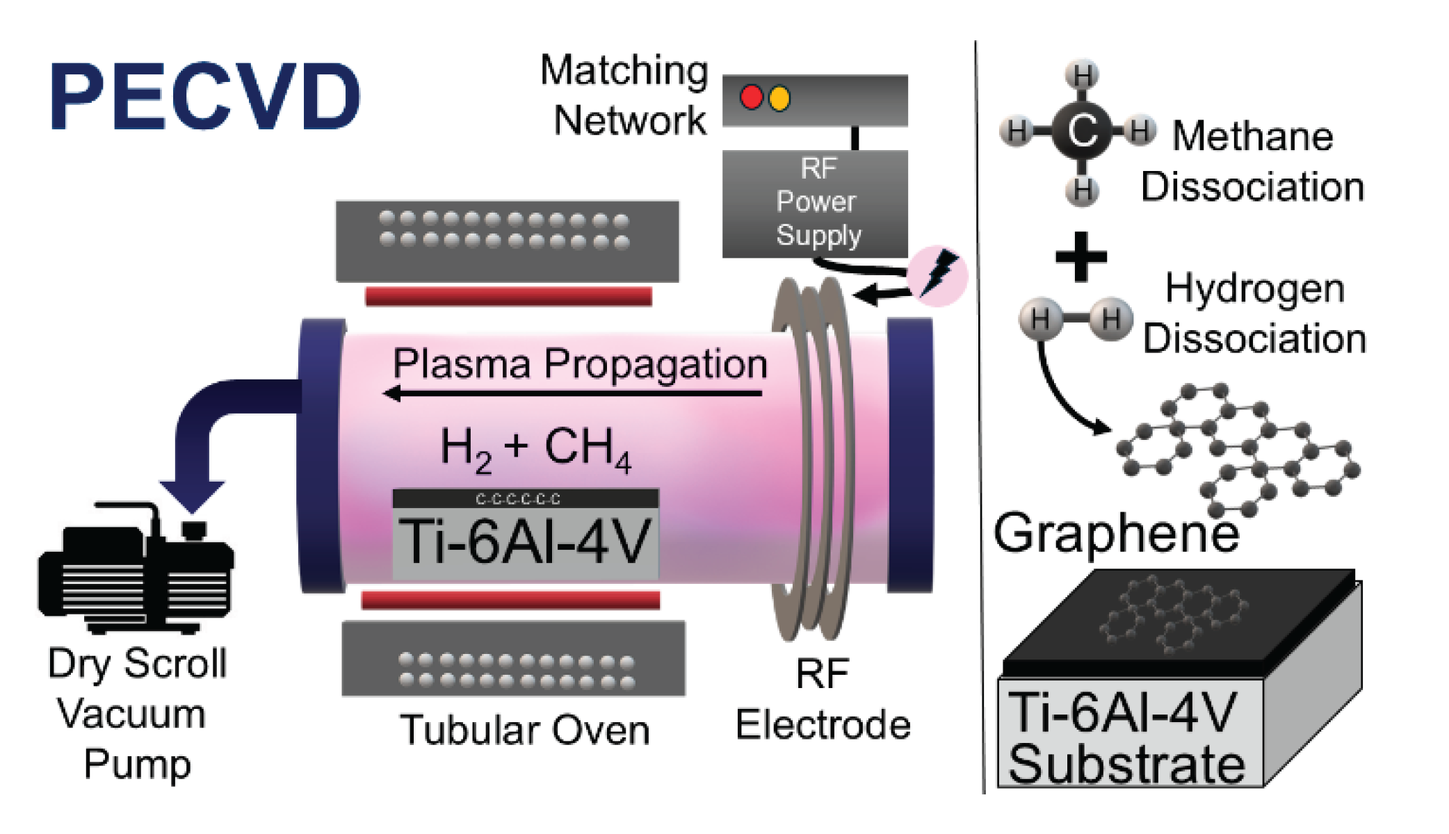
Figure 2.
Schematic of the Hot Tip TEP technique.
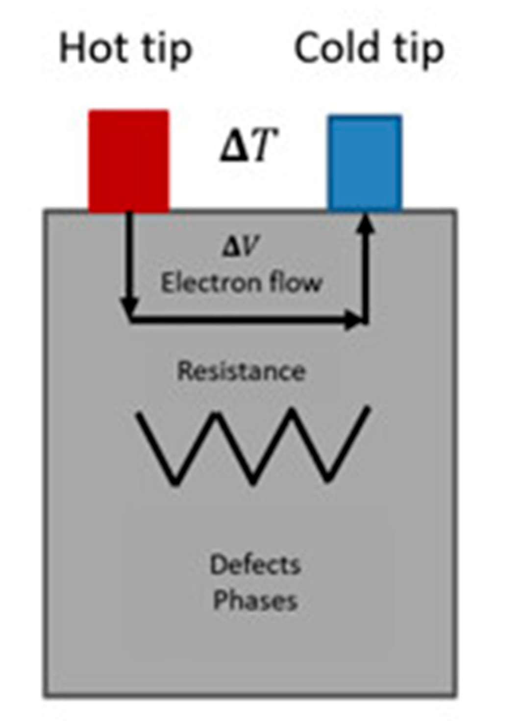
Figure 3.
A schematic diagram of detection at material imperfections by electromagnetic sensing.
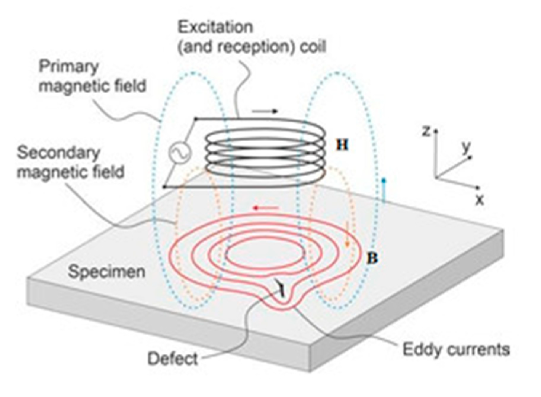
Figure 4.
Raman spectra of preliminary samples (Ti substrates) upon exposure to varying conditions.
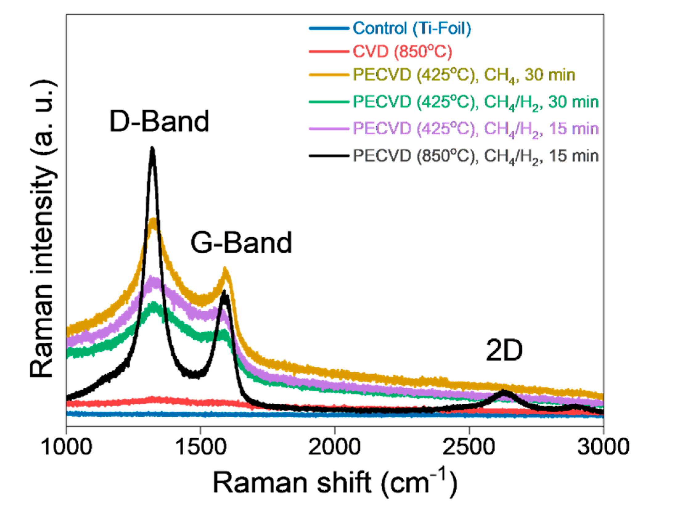
Figure 5.
Comparative analysis on growth (min); (a) PECVD deposition on control (Titania) sample with various time (3-30 min); (b) Raman spectroscopy of PECVD samples; (c) Intensity ratio (ID/IG); (d) Intensity ratio (I2D/IG); (e) Bar plot on D band; (f) bar plot on G band; (g) Bar plot on 2D band.
Figure 5.
Comparative analysis on growth (min); (a) PECVD deposition on control (Titania) sample with various time (3-30 min); (b) Raman spectroscopy of PECVD samples; (c) Intensity ratio (ID/IG); (d) Intensity ratio (I2D/IG); (e) Bar plot on D band; (f) bar plot on G band; (g) Bar plot on 2D band.
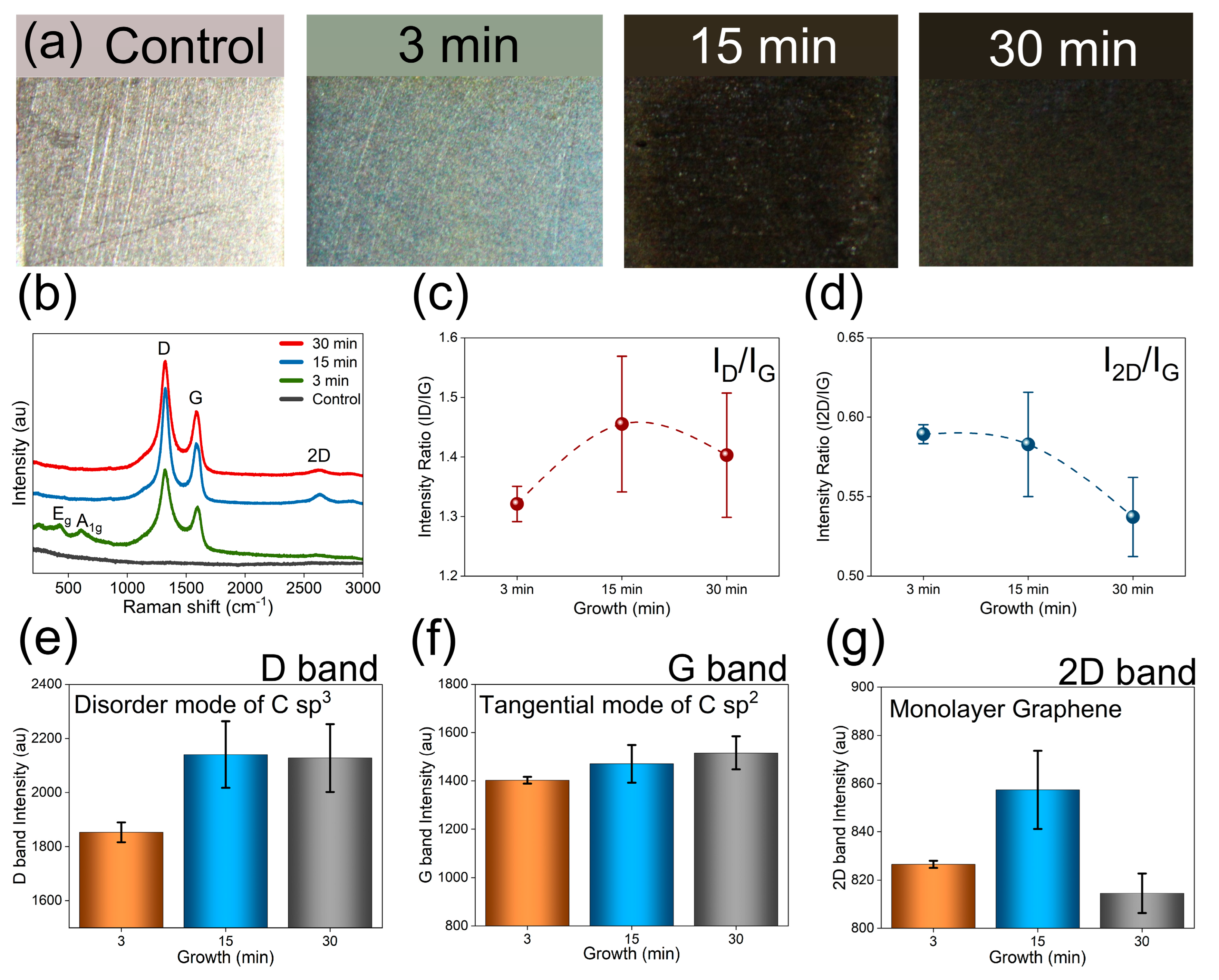
Figure 6.
Control Vs. PECVD Thin film morphological characteristics; (a) Raman spectroscopy; (b) X-ray Diffraction; (C) Atomic Force Microscopy (AFM), Plane XY= topography, Plane XYZ (Gradient represent Z-axis, height in micrometer); Control = Ti Foil, PECVD = 15 minutes plasma exposure at 150 Watts, equimolar feed ratio (CH4/H2 = 1), Oven temperature = 850 Degree Celsius, Pressure = 0.18 Torr. .
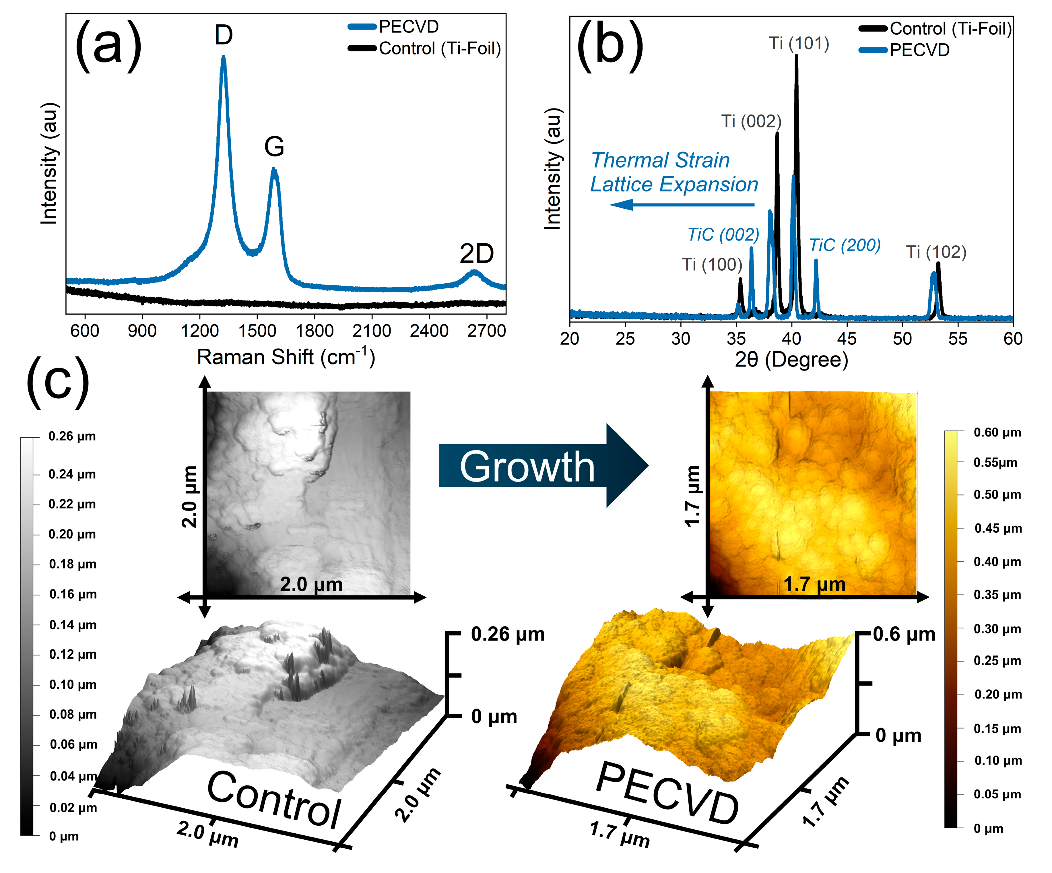
Figure 7.
TEP values for samples with low (LT), medium (MT) and high (HT) substrate thicknesses, and low (LR), medium (MR) and high (HR) surface roughness. a) Values for all samples with Cu tip. b) Values for all samples with Ni tip. c) Values for all samples with Au tip.
Figure 7.
TEP values for samples with low (LT), medium (MT) and high (HT) substrate thicknesses, and low (LR), medium (MR) and high (HR) surface roughness. a) Values for all samples with Cu tip. b) Values for all samples with Ni tip. c) Values for all samples with Au tip.
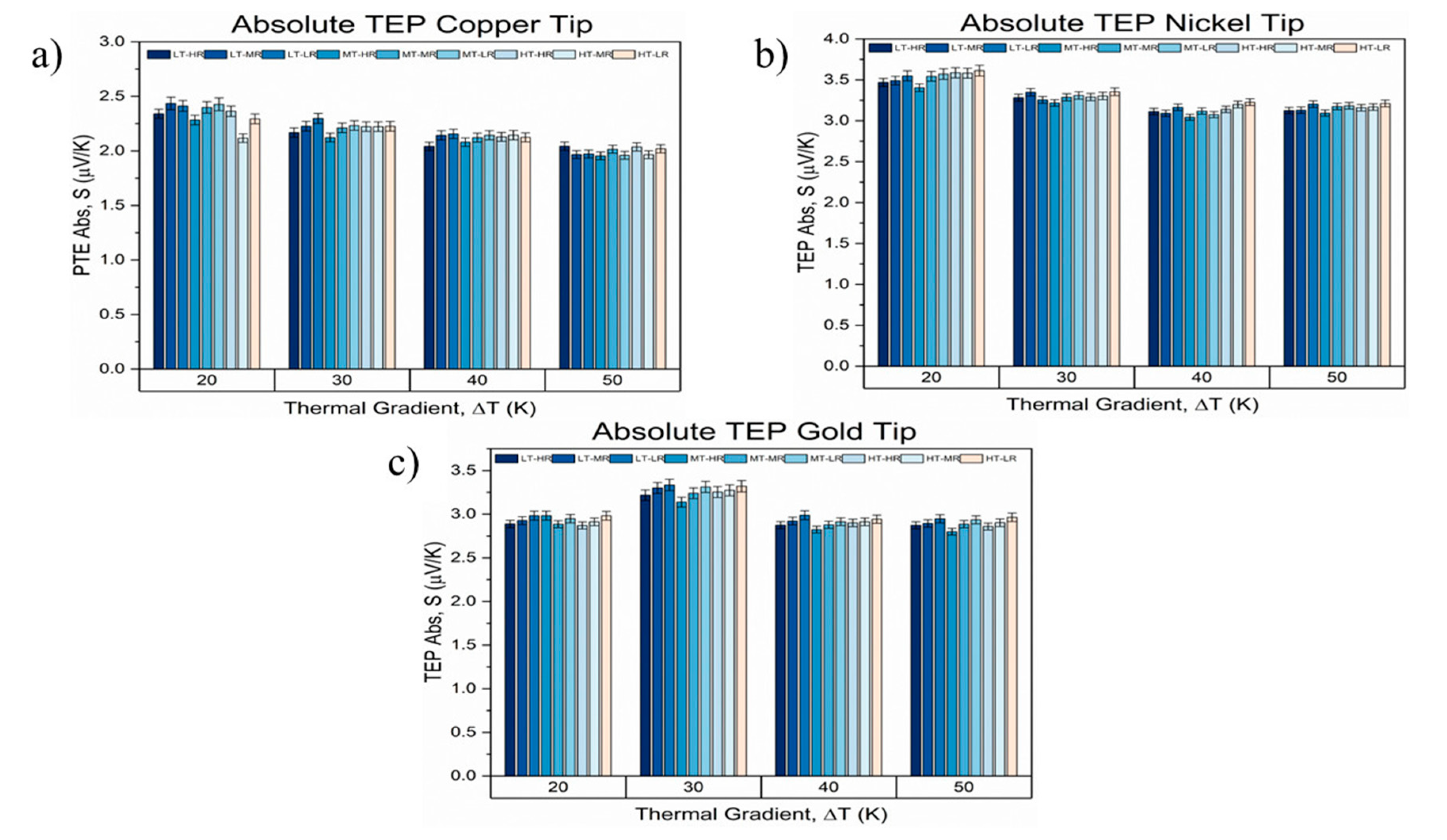
Figure 8.
Impedance plots for the Ti-6Al-4V ELI – Nanographene system at 50 KHz. a) High rugosity samples. b) Medium rugosity samples. c) Low rugosity samples.
Figure 8.
Impedance plots for the Ti-6Al-4V ELI – Nanographene system at 50 KHz. a) High rugosity samples. b) Medium rugosity samples. c) Low rugosity samples.
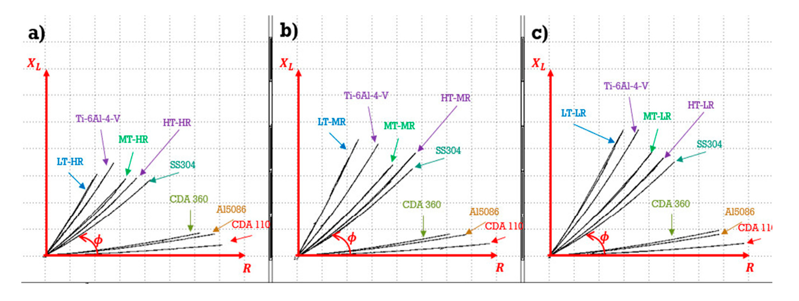
Figure 9.
Comparison of electrical conductivity values for Ti-6Al-4V ELI – Nanographene samples and base material.
Figure 9.
Comparison of electrical conductivity values for Ti-6Al-4V ELI – Nanographene samples and base material.
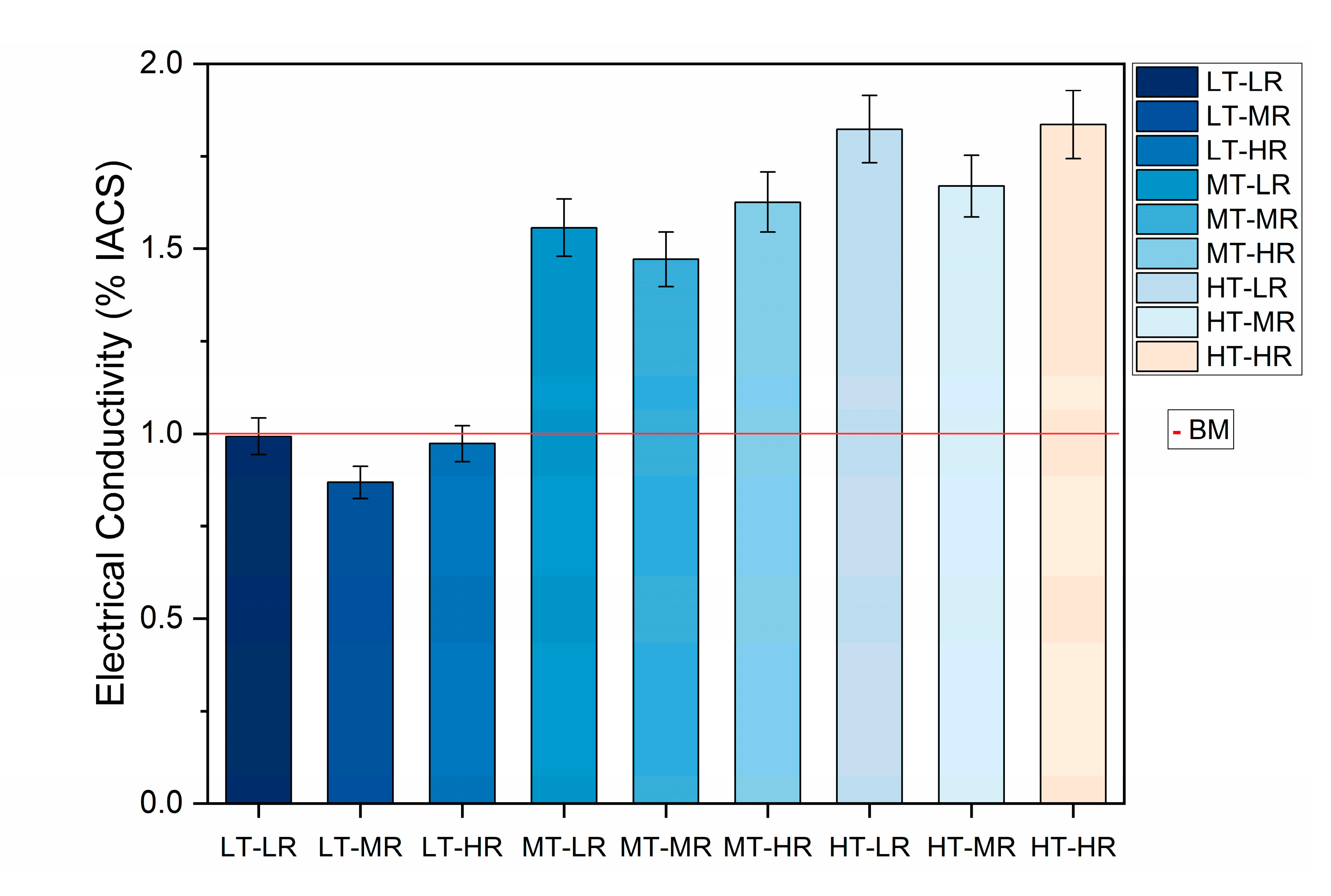
Figure 10.
SEM image of (a) nanographene coating on Ti-6Al-4V ELI substrate, (b) close-up image of nanographene coating on Ti-6Al-4V ELI substrate.
Figure 10.
SEM image of (a) nanographene coating on Ti-6Al-4V ELI substrate, (b) close-up image of nanographene coating on Ti-6Al-4V ELI substrate.
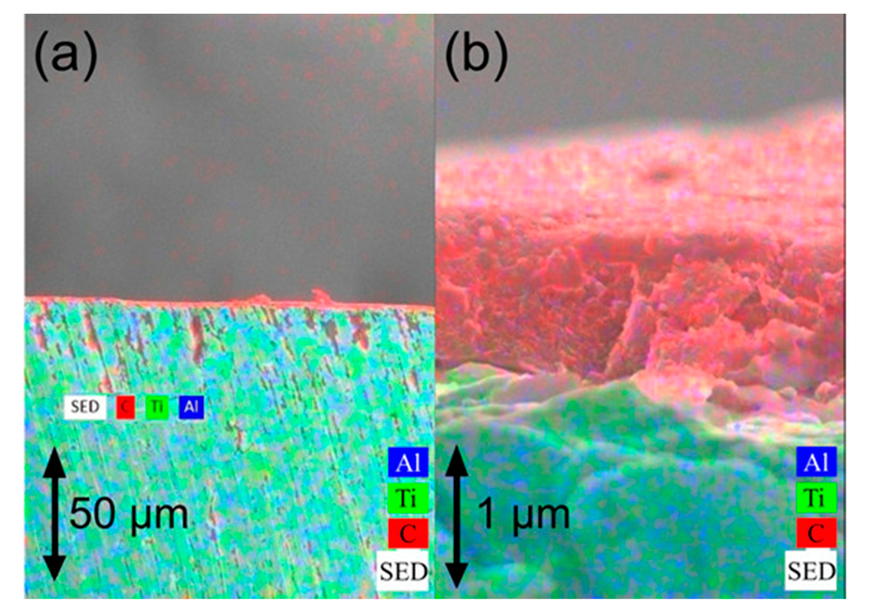
Figure 11.
Plausible mechanism pathway. Inspired by Ref.[94].
Figure 11.
Plausible mechanism pathway. Inspired by Ref.[94].
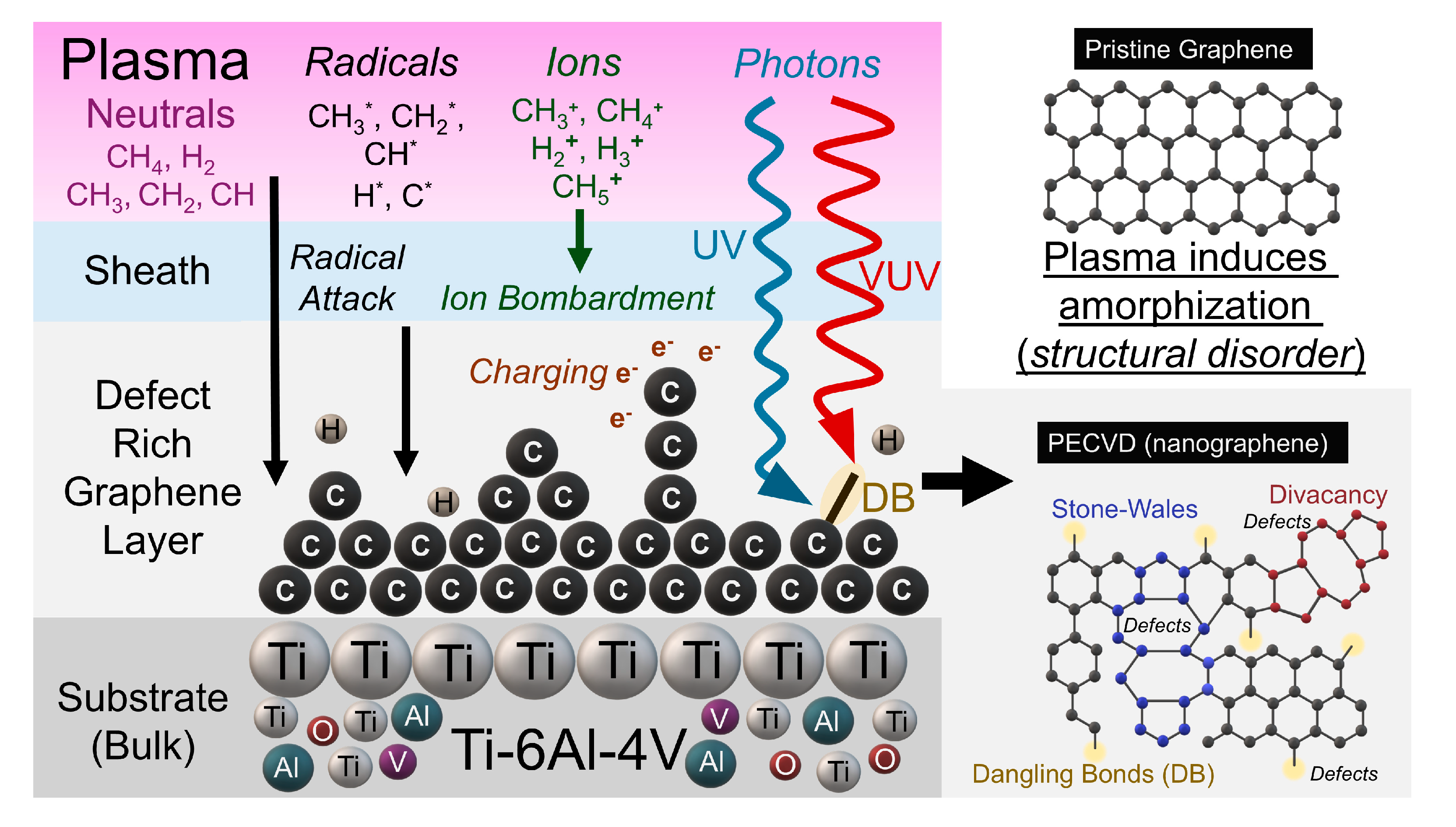
Figure 12.
Average surface roughness of Ti-6Al-4V ELI samples.
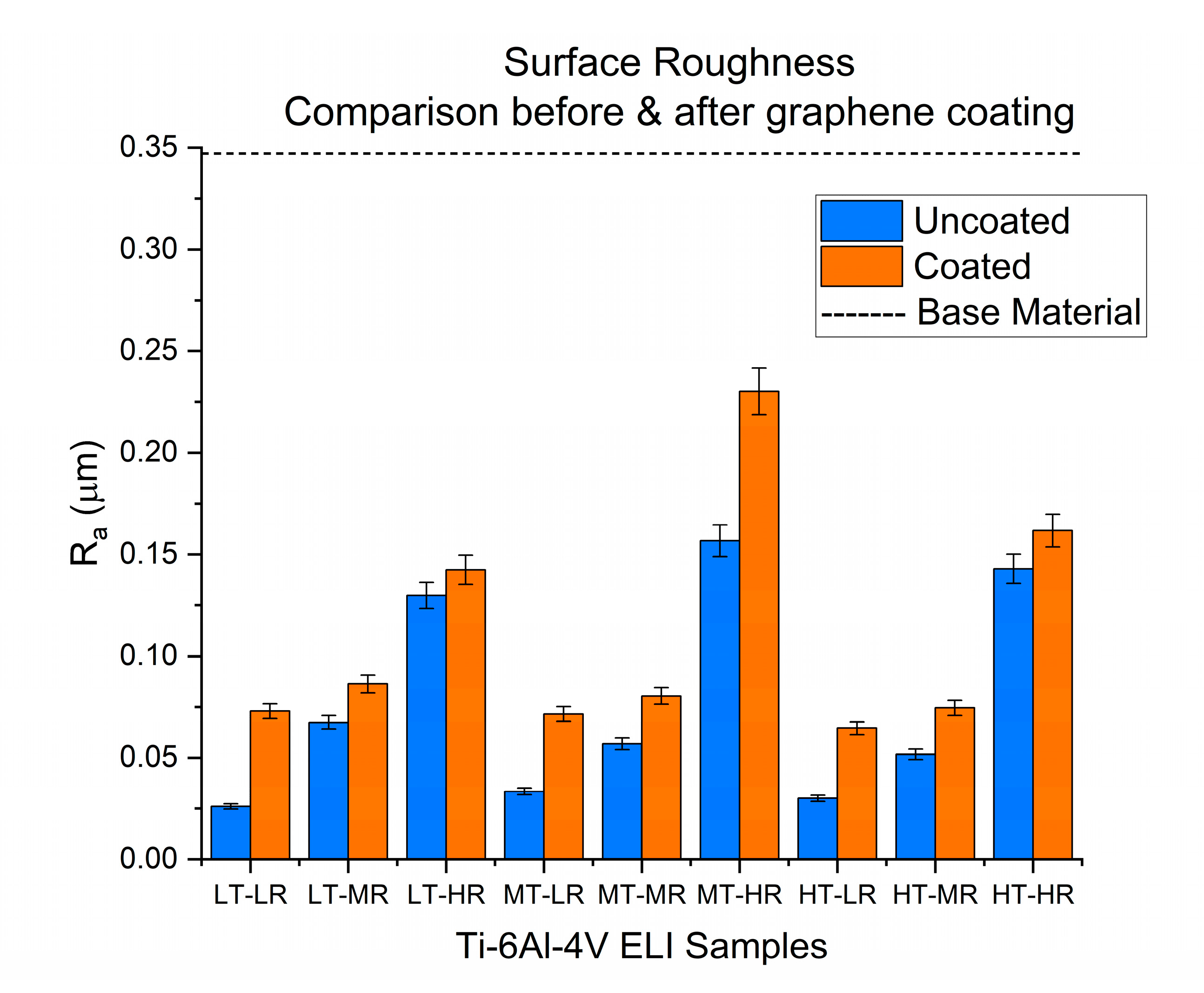
Disclaimer/Publisher’s Note: The statements, opinions and data contained in all publications are solely those of the individual author(s) and contributor(s) and not of MDPI and/or the editor(s). MDPI and/or the editor(s) disclaim responsibility for any injury to people or property resulting from any ideas, methods, instructions or products referred to in the content. |
© 2026 by the authors. Licensee MDPI, Basel, Switzerland. This article is an open access article distributed under the terms and conditions of the Creative Commons Attribution (CC BY) license (http://creativecommons.org/licenses/by/4.0/).
Copyright: This open access article is published under a Creative Commons CC BY 4.0 license, which permit the free download, distribution, and reuse, provided that the author and preprint are cited in any reuse.


