Submitted:
16 January 2026
Posted:
20 January 2026
You are already at the latest version
Abstract
Scandium-doped aluminum nitride (ScAlN) is a promising replacement for undoped aluminum nitride in MEMS vibration and acoustic sensors due to its higher piezoelectric coefficients, and for RF MEMS due to its enhanced piezoelectric response and ferroelectric switching capability. However, poor process conditions often lead to degraded film performance. In this work, we optimized the growth conditions of ScAlN thin films deposited by reactive pulsed-DC magnetron sputtering system by studying the impact of N₂ flow rate, target–substrate distance, substrate temperature, and substrate bias on film stress, crystallinity, and surface morphology. Based on stress measurements, XRD rocking curves along the c-axis (002), and roughness with AOG formation probability extracted from AFM and SEM images, an optimized deposition recipe was developed that balances stress, crystallinity, and AOG density. With this optimized recipe, samples were fabricated for dielectric, ferroelectric, and piezoelectric coefficient (d33,f and d31,f) measurements. To verify scalability, d33,f, εr, and tan(δ) were measured on 100, 150, and 200 mm substrates. Dual beam laser interferometry results showed d33,f values of around 18 pm/V, εr of 18, and lowest tan(δ) of 0.4%. Cantilever-based d31,f measurements yielded a value of −6.22 pC/N. The optimized ScAlN films also exhibited remnant polarization, Pr = 130 μC/cm², and coercive field, Ec = 3.5 MV/cm.
Keywords:
piezoelectricity
; ferroelectricity
; ScAlN
; thin films
; PVD
; sputtering
; DBLI
1. Introduction
Piezoelectric and ferroelectric materials play a pivotal role in microelectromechanical systems (MEMS), enabling critical functionalities in sensing [1,2,3], acoustic communication [4,5,6,7], and radio-frequency (RF) filtering [8,9,10]. Among these materials, aluminum nitride (AlN) has attracted substantial attention due to its high acoustic velocity [11], excellent thermal conductivity [11], and compatibility with complementary metal–oxide–semiconductor (CMOS) fabrication processes [12]. However, the relatively low piezoelectric coefficients of AlN limit its use in applications that require strong electromechanical coupling [13].
To address this limitation, extensive research has been conducted focused on enhancing the piezoelectric response of AlN through alloying and elemental doping. Among the various approaches, scandium (Sc) incorporation has proven particularly effective, significantly improving both the piezoelectric and ferroelectric properties of AlN and enabling its deployment in advanced acoustic and memory devices [14,15,16,17]. Early investigations using dual reactive co-sputtering demonstrated a noticeable enhancement in the piezoelectric response of Sc-doped AlN thin films [18,19,20]. Both ab initio models [21,22] and experimental studies [23] have shown that Sc concentrations up to 43% can yield up to a fourfold increase in the longitudinal piezoelectric coefficient (), achieving values of approximately . More recently, Lu et al. [24] reported a value of for 41% Sc-doped AlN, while Kenjita et al. [25] demonstrated that incorporating a lutetium (Lu) buffer layer can stabilize the wurtzite phase beyond the 43% Sc solubility limit, resulting in a of for 50.8% Sc-doped AlN.
Although extensive research has been conducted on optimizing ScAlN thin films to enhance their performance [26,27,28,29], a systematic study of how reactive sputtering process parameters affect film quality and performance is still lacking. In this work, the influence of process parameters—pressure, target–substrate distance, substrate temperature, and substrate RF power—on ScAlN thin films grown by reactive sputtering was experimentally investigated. To optimize the growth conditions, the mechanical, structural, and morphological properties of the films were characterized. Based on this analysis, an optimized deposition recipe was developed for this system and subsequently used to grow ScAlN thin films for detailed electrical and electromechanical characterization.
Nevertheless, most of the reported values in the literature have been obtained using a Berlincourt piezometer, which may not adequately account for substrate bending effects and electrode geometry [30,31]. In contrast, the double-beam laser interferometry (DBLI) technique employed in this work provides a more precise characterization of the piezoelectric response while compensating for substrate bending [32,33].
In addition, the transverse piezoelectric coefficient () was extracted using a digital holographic microscope (DHM) on a cantilever-based structure, where the tip displacement under electrical excitation was analyzed to compute via analytical formulations. Upon extracting the values of , , and , the figure of merit (FOM) for the cantilever-based system for energy harvesters and sensors was then calculated.
Beyond their enhanced piezoelectric response, ScAlN films have also been shown to exhibit robust ferroelectric behavior [34,35,36,37], unlocking their potential in non-volatile memory and tunable RF components [38,39,40,41,42,43]. In this work, the dielectric (, ) and ferroelectric (, ) properties of ScAlN thin films deposited under optimized process conditions were also investigated.
2. Deposition & Characterization Procedure
ScAlN thin films were deposited on 100 mm silicon (Si) (100) wafers using an Evatec® Clusterline-200 II magnetron sputtering system operated under high-vacuum conditions (). A 12-inch casted Sc0.3Al0.7 alloy target was employed as the sputtering source. Deposition parameters—including chuck temperature, nitrogen (N2) flow rate, and chuck height—were systematically varied to study their effects on film growth. The target was powered by a pulsed DC source at 5 kW, 100 kHz, with an 84% duty cycle.
To optimize the deposition process, the target–substrate distance (chuck height) was adjusted while other conditions were kept constant. Deposition rates at each chuck height were determined under an N2 flow of 20−35 sccm. Film thickness—and thus deposition rate—was measured using a Woollam ESM-300 ellipsometer, which evaluates thin-film thickness by analyzing polarization response as a function of thickness and refractive index [44]. Argon (Ar) was excluded to avoid abnormally oriented grain (AOG) formation, as reported in literature [20,24]. Surface morphology and AOG presence were examined using a Zeiss Supra 25 FE-SEM and Park XE-7 AFM. Depositions were performed in pure nitrogen (N2) at 20–35 sccm while keeping chuck height and temperature constant to study the effect on stress and crystallinity. We characterized the deposited films with a series of measurements. Film stress was measured with a KLA-Tencor FLX-2320 by comparing substrate curvature before and after deposition and applying Stoney’s equation [45]. X-ray diffraction (XRD) was carried out on ScAlN thin films deposited on Si (100) substrates using a PANalytical X’Pert Pro diffractometer with a Philips PW3040/60 X-ray generator and detector. Diffraction patterns were collected using Cu-K radiation (). 2 scans identified the crystallographic planes, while rocking curve (fwhm of the -scan curve) measurements assessed the film crystallinity. The correlation between c-axis alignment and piezoelectric performance in ScAlN films, reported by Tholander et al. [46], guided the optimization of deposition conditions.
A temperature sweep (250°C, 300°C, 350°C, and 400°C) was then performed to evaluate the influence of growth temperature on film quality. Once the deposition conditions yielding optimal crystallinity were identified, substrate RF power was adjusted to minimize residual stress. After optimizing the ScAlN deposition process, samples were fabricated for subsequent dielectric, piezoelectric, and ferroelectric characterization.
After optimizing the recipe for ScAlN thin films on Si 100 mm wafers, two different samples were prepared for the dielectric, ferroelectric, and piezoelectric measurements. Sample type-1 was used for dielectric, ferroelectric, and longitudinal piezoelectric coefficient () measurements. Figure 1(a) and Figure 1(b) represent the cross-sectional and top-view schematics of Sample type-1, respectively. It comprised a 50 nm blanket Pt bottom electrode, a 750 nm ScAlN layer, and a 50 nm Pt top electrode patterned to define metal–piezoelectric–metal (MPM) capacitors with circular and square geometries of various areas. Electrical access to the blanket bottom electrode was provided by deliberately removing a small region of the piezoelectric layer (by mechanical scratching) and applying indium (In) paste to this exposed area to ensure good grounding.
The longitudinal piezoelectric response of the ScAlN films was characterized using an aixACCT double-beam laser interferometer (DBLI). In this configuration, the coefficient was extracted, quantifying the voltage-dependent longitudinal displacement of the piezo layer while compensating for substrate bending. The ferroelectric properties—remnant polarization (), and coercive field () of ScAlN film—were studied using the same aixACCT system. Dielectric relative permittivity () and dielectric loss (tan) were also measured using this sample. To evaluate the consistency of the measurement results over different substrate sizes, we fabricated two more samples on 150 mm and 200 mm substrates using the same stacks, methods, and electrode patterns as sample type-1.
Meanwhile, as shown in Figure 1(c),Figure 1(d), sample type-2 was fabricated as an asymmetric laminate configured as a cantilever to extract the transverse piezoelectric coefficient (). In this work, a cantilever-based approach was employed owing to its simplicity and its suitability for direct extraction of the transverse piezoelectric coefficient (). The cross-sectional schematic and SEM top-view of sample type-2 are shown in Figure 1(c) and Figure 1(d), respectively. Prior studies have shown that a cantilever architecture provides a straightforward and reliable means of directly estimating the transverse piezoelectric coefficient of the piezoelectric layer in a multilayer stack [7,47].
The fabricated cantilever consists of a rectangular Metal–Piezoelectric–Metal (MPM) stack. Unlike conventional designs that use a structural layer and symmetric top/bottom electrodes of equal thickness, an asymmetric electrode configuration was employed here to facilitate excitation of the bending mode. Specifically, a 200 nm Pt layer was deposited as the bottom electrode, followed by the piezoelectric film, and finally a 100 nm Pt layer as the top electrode.
To account for the influence of these additional layers in the mechanical and electromechanical response, the multimorph model is employed [47]. In this framework, the first step is to determine the location of the neutral axis for bending in the multilayered structure. This neutral axis is obtained by evaluating the torque equilibrium across all constituent layers, expressed as:
where denotes the z-position of the torque neutral axis (with z defined as the direction perpendicular to the beam surface). The summation is taken over all layers in the device stack. For each layer i, represents the position of its centroid, is its Young’s modulus, and is its cross-sectional area, where and are the width and thickness of layer i, respectively. The displacement of the tip of the cantilever can be expressed as:
where is the position of the centroid of the layer i with respect to the neutral axis, and V is the applied voltage. From this relation, the tip displacement can be treated as a quantity that is directly proportional to the applied voltage V. When a DC bias is applied across the cantilever beam, the resulting tip deflection can be recorded to generate a –V curve, which is subsequently fitted using a linear regression. The transverse piezoelectric coefficient can then be extracted from the fitted slope according to
where is the experimentally obtained slope of the –V relation, and m is the geometric factor determined by the multimorph model.
Furthermore, upon extracting the values of , , and , the figure of merit (FOM) for the cantilever-based system was calculated. To compare the efficiency of piezoelectric layers in cantilever-based systems for energy harvesters and sensors, a suitable FOM method was defined by Priya [48,49], which can be expressed as:
This serves as a useful parameter for applications in energy harvesting and low noise sensors, which we use to quantify our films.
3. Results
3.1. Process Optimization
For stress optimization, ScAlN films were deposited on 100 mm Si (100) substrates and subsequently analyzed. Ellipsometric measurements confirmed a film thickness of approximately 500 nm with a deviation of . Figure 2 presents the stress behavior of the films under varying process conditions, including nitrogen flow rate, chuck height, substrate temperature, and substrate RF power.
From Figure 2(a), it can be seen that at nitrogen flow rates of 20 sccm and 25 sccm, the films exhibited slightly compressive stresses of about −20 MPa, while at 30 sccm and 35 sccm, the stress shifted to slightly tensile values of +23 MPa and +11 MPa, respectively. This indicates that increasing the gas flow rate has a minimal influence on the overall stress state of the films. In contrast, varying the target–substrate distance (chuck height) from 10 mm to 30 mm significantly changed the stress from −252 MPa (compressive) to +191 MPa (tensile) (Figure 2(b)). At constant nitrogen flow rate and temperature, the stress tends to become more tensile with increasing target–substrate distance.
As shown in Figure 2(c), the stress remains relatively stable between and ; however, a compressive stress of −181 MPa is observed at . Although the lowest overall stress was obtained at a chuck height of 20 mm, determining the optimal process condition requires considering additional deposition parameters and material characterization results. From Figure 2(d), it is evident that the film stress demonstrates a strong dependence on RF power. Increasing the substrate RF power from 0 to 100 W drives the stress from near-zero values to approximately –1.8 GPa compressive. However, the RF power applied to the substrate does not have any impact on the film’s crystallinity [50]. Therefore, the stress could be optimized by tuning RF power on the substrate without affecting the film quality.
Figure 3(a)–(c) illustrate the variation in the peak position of the ScAlN wurtzite (002) phase under different process conditions. As shown in Figure 3(a)–(c), the (002) diffraction peak shifts toward higher angles with increasing flow rate, target–substrate distance, and temperature, indicating a reduction in lattice spacing of the ScAlN crystals.
The crystallinity of the films was further assessed by analyzing the full width at half maximum (FWHM) values obtained from XRD -scans (rocking curves) under different process conditions, as depicted in Figure 3(d)–(f). Figure 3(d) highlights the effect of flow rate on the film quality. The best crystallinity (lowest RC) was observed at 20 sccm, yielding an FWHM value of . Higher nitrogen flow rates produced broader peaks (2.8°, 3.4°, and 3.8° for 25, 30, and 35 sccm, respectively), reflecting a deterioration in crystalline quality. Considering the strong correlation between crystallinity and device performance [51], a nitrogen flow rate of 20 sccm was selected for subsequent process optimization.
Figure 3(e) presents the effect of target–substrate distance on crystallinity. Optimal film quality was achieved at distances of 20 mm and 25 mm, yielding a rocking curve (RC) value of . Both shorter and larger distances resulted in peak broadening, indicating inferior crystallinity. Hence, a range of 20–25 mm was identified as the preferred chuck height for future depositions to balance stress and crystallinity.
The influence of deposition temperature, shown in Figure 3(f), was found to be relatively minor compared to the other parameters. The optimal temperature was determined to be , with an RC value of .
To identify the crystallographic phases present in the deposited ScAlN film and to verify the reproducibility of the optimized parameters, films were also deposited on Si/Pt substrates. A gonio (2) scan was performed for sample type-1, as shown in Figure 4(a), to determine the crystallographic phases. As shown in Figure 4(b), the crystalline quality remained consistent, with RC values ranging from to across the 100 mm, 150 mm, and 200 mm substrates, confirming the scalability and uniformity of the deposition process.
The presence of abnormally oriented grains (AOGs) was observed by SEM to assess the surface quality of films deposited on Si (100) substrates. Previous studies report that the density of AOGs increases with Sc content in the film [52,53]. A high concentration of AOGs leads to increased surface roughness, degraded film quality, and a reduction in both piezoelectric response and quality factor in piezoelectric acoustic resonators [54,55].
To understand how the deposition parameters influence AOG formation, the SEM images were analyzed using an image recognition algorithm specifically developed for the quantitative assessment of AOGs [56]. This method enables pixel-level detection of individual grains on the substrate and allows precise calculation of their average area and surface coverage. Figure 5 shows the resulting AOG area distributions. A leftward shift of the peak in the distribution indicates a higher fraction of smaller AOGs. Narrow, sharp peaks correspond to a more uniform grain size, whereas broader curves reflect a wider spread of AOG areas. These quantitative distributions support the qualitative impressions obtained from direct visual inspection of the SEM images. Figure 5(a) and (b) illustrate the transformation from a raw SEM image, where AOGs are visually apparent, to the corresponding pixel-level grain detection map.
Figure 5(c) presents the AOG area probability density as a function of N2 flow rate. At 30 sccm and 35 sccm, the distribution shifts to smaller areas and becomes narrower compared to 20 sccm and 25 sccm, indicating that higher N2 flow promotes the formation of smaller grains. However, the overall probability of AOG occurrence is higher at these elevated N2 flow rates. At 20 sccm, the average AOG size is larger, but the probability of AOG formation is comparatively low. At 25 sccm, the AOG density remains relatively low compared to 30–35 sccm, but the range of AOG areas is broader. Taken together, these observations suggest that 20 sccm N2 offers a more favorable trade-off than higher flow rates in terms of minimizing AOG formation.
The effect of target–substrate distance is shown in Figure 5(d). Varying the distance from 10 mm to 25 mm has only a modest impact on AOG probability; however, at 30 mm the AOG formation probability increases, with a larger number of smaller AOGs appearing. Temperature exhibits a similarly limited influence on AOG density (Figure 5(e)). At higher temperatures, the overall AOG probability decreases slightly, but the distribution broadens, indicating a wider range of AOG sizes.
In contrast, the RF substrate power sweep, shown in Figure 5(f), has a much more pronounced effect. Increasing the RF power substantially reduces the AOG formation probability, ultimately yielding films that are nearly AOG-free at 100 W. This improvement, however, comes at the cost of increased compressive stress, which reaches approximately −1.8 GPa at 100 W shown in Figure 2(d). Considering this trade-off between surface quality and residual stress, no RF power was applied to the substrate in the final optimized process recipe used in this study.
Overall, the best process conditions for achieving superior crystallinity in ScAlN thin films on 100 mm substrates, considering stress−AOG growth probability tradeoff, were identified with a nitrogen flow rate of 20 sccm, a target–substrate distance of 20 mm, and a deposition temperature of .
Since one of the goals of this ScAlN film optimization was to design a device that requires a bimorph ScAlN structure, determining the influence of vacuum breaking between successive depositions for each layer growth is a critical factor for film quality. The surface morphology of two ScAlN samples deposited on Si/Pt substrates was analyzed using atomic force microscopy (AFM) over a scan area of . In this experiment, two ScAlN layers were sequentially deposited on Si/Pt substrates, separated by an intermediate 50 nm platinum layer, to evaluate the impact of vacuum interruption on film growth. For these depositions, the N2 flow was set to 20 sccm, the chuck height to 20 mm, and the substrate temperature to 350°C, while no RF power was applied to the substrate.
Figure 6(a) presents the top surface morphology of the second ScAlN layer deposited after breaking the vacuum between the successive deposition steps, whereas Figure 6(b) illustrates the corresponding surface obtained under in situ conditions (continuous deposition without vacuum interruption). The rougher surface observed in Figure 6(a) demonstrates the adverse effect of vacuum breaking on bimorph ScAlN film growth, resulting in larger grain size and reduced grain density.
To mitigate surface roughness and grain enlargement, the deposition temperature was reduced from to . As reported by Jin et al. [57], elevated substrate temperatures as well as low temperatures can suppress uniform columnar growth in AlN films. Figure 6(c) shows the ScAlN film surface, featuring smaller, well-aligned columnar grains with higher grain density and a reduced RMS roughness of 1.6 nm. These improvements confirm that optimized temperature control is essential for achieving high-quality bimorph ScAlN layers. Table 1 refers to the investigation range and optimized process parameters for the ScAlN thin film deposition procedure.
3.2. Dielectric Properties
Figure 7(b),(c) illustrate the relative permittivity () and dielectric loss tangent () of the ScAlN films deposited on substrates of different diameters. The relative permittivity values obtained from DBLI measurements are 19.4, 18.2, and 18.0 for the 100 mm, 150 mm, and 200 mm samples, respectively. The dielectric loss tangent showed the highest value () for the 100 mm film, while the 150 mm and 200 mm films exhibited lower losses as and , respectively.
The observed variation in dielectric loss directly influences the measured piezoelectric coefficient. As shown in Figure 7(a), samples with lower dielectric loss exhibited higher values, highlighting the strong dependence between dielectric dissipation and effective piezoelectric response in ScAlN thin films.
3.3. Measurement of Piezoelectric Strain Coefficients
3.3.1. Longitudinal Piezoelectric Coefficient ()
The longitudinal piezoelectric coefficient () of ScAlN films deposited on substrates of three different diameters was measured using double-beam laser interferometry (DBLI). The extracted values ranged from 17.6 pm/V to 18.7 pm/V, as shown in Figure 7(a) for 100 mm, 150 mm, and 200 mm substrates. During measurement, a 1 kHz AC voltage was applied to the circular top electrode to induce piezoelectric displacement, while the bottom electrode was grounded. The input voltage amplitude was maintained below the polarization switching threshold, ensuring that the displacement response remained linear with the applied electric field, consistent with conventional piezoelectric behavior shown in Figure 8(a).
However, Yuan et al. [24] demonstrated that the density of abnormally oriented grains (AOGs) degrades the piezoelectric coupling in ScAlN, with films exhibiting more than 100 AOGs per showing a reduction in by approximately compared to well-oriented crystals. In the present study, SEM and AFM analysis shown in Figure 5 and Figure 6 revealed an AOG density below this threshold, suggesting that the measured values are close to those expected for an ideal wurtzite crystal.
3.3.2. Transverse Piezoelectric Coefficient ()
After device release for sample type 2, a DC bias voltage was applied between the top and bottom electrodes, and the resulting out-of-plane displacement at the cantilever tip was measured using digital holographic microscopy (DHM). The measured displacement–voltage response, shown in Figure 7(d), was then fitted to extract the effective transverse piezoelectric coefficient of the film, , at each measurement point using Equation (2).
By repeating this procedure for cantilevers of varying lengths, a clear convergence trend was observed in Figure 7(e): as the aspect ratio () increases, the extracted shifts from a plane-strain-dominated value (approximately 30% higher than the uniaxial constant ) towards the intrinsic uniaxial material constant of the film, . This behavior is consistent with the expected behavior reported by Hake et al. [49]. For structures with small ratios, the mechanical response deviates from pure beam behavior and becomes more plate-like, and the effective converges toward the plane-strain value, approaching . As increases, the geometry more closely approximates the uniaxial stress state assumed in the beam theory, and the fitted converges toward the intrinsic material property, reaching approximately .
3.4. Ferroelectric Properties
Using the same DBLI experimental setup, dynamic hysteresis measurements (DHM) were performed to evaluate the polarization switching characteristics of the ScAlN films. The resulting P–E hysteresis loop (Figure 8(c)) clearly demonstrates ferroelectric behavior, showing an average remnant polarization of and an average coercive field of . This reversible switching of polarization under an alternating electric field confirms the intrinsic ferroelectric nature of the material. Additionally, the nonlinear Voltage−Displacement curve (Butterfly Curve) presented in Figure 8(b) is evidence of the ferroelectric nature of ScAlN. This graph illustrates the nonlinear piezoelectric response, demonstrating the material’s displacement when subjected to an electric field surpassing the coercive field (Ec). The characteristic butterfly-shaped voltage–displacement curve indicates the ferroelectric behavior of ScAlN. The observed nonlinearity results come from the reorientation of dipoles under electric fields exceeding Ec, where the material demonstrates maximum displacement while considerable ferroelectric domain switching takes place.
To further analyze the switching dynamics, Dynamic Hysteresis Measurement (DHM) and Positive-Up-Negative-Down (PUND) measurements were conducted, as shown in Figure 8(c),(d). As the applied field exceeds the coercive field, domain walls progressively align with the external field direction, producing a characteristic rise in polarization. When the field polarity was reversed, domains switched correspondingly from N-polar to M-polar orientation (or vice versa).
Distinct switching current peaks were observed at the coercive field points in both Figure 8(c),(d), indicating rapid polarization reversal once the energy barrier for domain wall movement was overcome [58]. These peaks arise from displacement currents proportional to the rate of polarization change, confirming the active ferroelectric switching process. A slight asymmetry was observed in Figure 8(c), between the positive and negative coercive fields (, ), consistent with findings by Liu et al. [59], who reported similar asymmetry even in capacitors with identical Al/AlScN/Al electrodes. This suggests that factors such as stress distribution within the film [60] may contribute to asymmetric switching behavior.
In the present study, higher remnant polarization and coercive field values were observed under negative bias, suggesting the presence of a built-in potential induced by residual stress, which impedes switching in the opposite direction. Additionally, as indicated by the green lines in Figure 8(d), leakage current was evident in both bias directions. This leakage contribution likely inflated the apparent remnant polarization value, resulting in the measured . Although the precise quantitative influence of leakage current was not measured in the present PUND analysis, its contribution to the measured polarization value is evident.
Table 2 showcases a comparative evaluation of the dielectric, piezoelectric, and ferroelectric properties of ScAlN along with the figure of merit (FOM).
4. Conclusion
This work has demonstrated a process-optimization methodology for ScAlN thin films grown by reactive pulsed DC magnetron sputtering on Si(100) substrates using a 12 inch casted target. The influence of key process parameters −N2 flow rate, target−substrate distance, substrate temperature, and RF power applied to the substrate on film stress, crystallinity, and surface morphology has been investigated systematically. On the basis of measured stress, XRD rocking curve values along the c-axis (002), and the estimated roughness and probability of abnormally oriented grains (AOG) formation from SEM and AFM analysis, an optimized deposition recipe was established while carefully balancing the trade-offs between stress, crystallinity, and AOG density. Using this optimized recipe (Table 1), two sets of samples were fabricated: one used for dielectric, ferroelectric, and longitudinal piezoelectric () characterization, and another for transverse piezoelectric () measurements. To assess the scalability and consistency of the process, , , and were measured on films deposited on 100, 150, and 200 mm substrates. DBLI measurements yielded values in the range of –, while the relative permittivity ranged from 18 to 19.4 and the loss tangent from 0.4% to 1.1% across the three substrate sizes. Cantilever-based measurements provided a value of , in good agreement with previously reported simulation data. The optimized ScAlN films also exhibited a ferroelectric response, with an average remanent polarization and coercive fields ranging from to . These results collectively demonstrate that the developed process enables the reproducibility of high-quality ScAlN thin film deposition over different wafer-scale substrates, making them strong candidates for next-generation MEMS devices for mass production.
Author Contributions
Conceptualization, K.S. and C.T.; methodology, K.S., C.T., and S.G.; software, K.S. and C.T.; validation, K.S., C.T., K.G., S.G., and M.R.; formal analysis, K.S. and C.T.; investigation, K.S. and C.T.; resources, S.G. and M.R.; data curation, K.S. and C.T.; writing—original draft preparation, K.S. and C.T.; writing—review and editing,K.S., K.G., S.G., and M.R. ; visualization, K.S.; supervision, K.G., S.G., and M.R.; project administration, K.G., S.G., and M.R.; funding acquisition, K.G., S.G., and M.R.. All authors have read and agreed to the published version of the manuscript.
Funding
This research was funded by the National Institutes of Health, United States. The grant number is NIH-R01DC-021596. The APC was funded by MDPI.
Data Availability Statement
Experimental data is available upon request to corresponding Author.
Acknowledgments
The authors thank the Kostas Nanoscale Technology and Manufacturing Research Center cleanroom facility and it’s staff for providing the support and required infrastructure for this experimental study.
Conflicts of Interest
The authors declare no conflicts of interest.
References
- Muralt, P.; Polcawich, R.G.; Trolier-McKinstry, S. Piezoelectric Thin Films for Sensors, Actuators, and Energy Harvesting. MRS Bulletin 2009, 34, 658–664. [Google Scholar] [CrossRef]
- Fawzy, A.; Zhang, M. Piezoelectric Thin Film Materials for Acoustic MEMS Devices. In Proceedings of the 2019 6th International Conference on Advanced Control Circuits and Systems (ACCS) & 2019 5th International Conference on New Paradigms in Electronics & information Technology (PEIT), 2019; pp. 82–86. [Google Scholar] [CrossRef]
- Ayed, F.B.; Giribaldi, G.; Venditti, A.; Saha, K.; Simeoni, P.; Qian, Z.; Rinaldi, M. Enhanced Infrared Sensing With 30Acoustic Delay Lines Integrated with Metamaterial Absorbers. In Proceedings of the 2024 IEEE Ultrasonics, Ferroelectrics, and Frequency Control Joint Symposium (UFFC-JS), 2024; pp. 1–4. [Google Scholar] [CrossRef]
- Xue, Y.; Liu, Y.; Zhou, C.; Zhang, X.Y. Acoustic wave devices based on piezoelectric/ferroelectric thin films for high-frequency communication systems and sensing applications. Ceramics International The 13th Asian Meeting on Ferroelectrics jointly with the 13th Asian Meeting on Electroceramics, 2024; 50, pp. 52051–52058. [Google Scholar] [CrossRef]
- Anderson, I.; Barrera, O.; Ravi, N.; Matto, L.; Saha, K.; Dasgupta, S.; Campbell, J.; Kramer, J.; Kwon, E.; Hsu, T.H.; et al. Solidly Mounted Scandium Aluminum Nitride on Acoustic Bragg Reflector Platforms at 14–20 GHz. IEEE Transactions on Ultrasonics, Ferroelectrics, and Frequency Control 2025, 72, 656–662. [Google Scholar] [CrossRef] [PubMed]
- Barrera, O.; Ravi, N.; Saha, K.; Dasgupta, S.; Campbell, J.; Kramer, J.; Kwon, E.; Hsu, T.H.; Cho, S.; Anderson, I.; et al. 18 GHz Solidly Mounted Resonator in Scandium Aluminum Nitride on SiO2/Ta2O5 Bragg Reflector. Journal of Microelectromechanical Systems 2024, 33, 711–716. [Google Scholar] [CrossRef]
- Littrell, R.; Grosh, K. Modeling and Characterization of Cantilever-Based MEMS Piezoelectric Sensors and Actuators. Journal of Microelectromechanical Systems 2012, 21, 406–413. [Google Scholar] [CrossRef]
- Muralt, P. Recent Progress in Materials Issues for Piezoelectric MEMS. Journal of the American Ceramic Society 2008, 91, 1385–1396. [Google Scholar] [CrossRef]
- Azarnaminy, A.F.; Ou, M.; Mansour, R.R. PCM-Based Reconfigurable Acoustic Resonators and Filters: For Potential Use in RF Front-End Applications. IEEE Microwave Magazine 2024, 25, 48–67. [Google Scholar] [CrossRef]
- Spagnuolo, L.; Saha, K.; Simeoni, P.; Colombo, L.; Rinaldi, M. 18 GHz Filters based on Cross-Sectional Lamé Mode Resonators (CLMRs). In Proceedings of the 2025 IEEE International Ultrasonics Symposium (IUS), 2025; pp. 1–3. [Google Scholar] [CrossRef]
- Tabrizian, R.; Rais-Zadeh, M.; Ayazi, F. Effect of phonon interactions on limiting the f.Q product of micromechanical resonators. In Proceedings of the TRANSDUCERS 2009 - 2009 International Solid-State Sensors, Actuators and Microsystems Conference, 2009; pp. 2131–2134. [Google Scholar] [CrossRef]
- Haider, S.T.; Shah, M.A.; Lee, D.G.; Hur, S. A Review of the Recent Applications of Aluminum Nitride-Based Piezoelectric Devices. IEEE Access 2023, 11, 58779–58795. [Google Scholar] [CrossRef]
- Manna, S.; Talley, K.R.; Gorai, P.; Mangum, J.S.; Zakutayev, A.; Brennecka, G.L.; Stevanović, V.; Ciobanu, C.V. Enhanced piezoelectric response of aln via crn alloying. Physical Review Applied 2018, 9. [Google Scholar] [CrossRef]
- Wingqvist, G.; Tasnádi, F.; Žukauskaitė, A.; Birch, J.; Arwin, H.; Hultman, L. Increased electromechanical coupling in w - scxal1-xn. Applied Physics Letters 2010, 97. [Google Scholar] [CrossRef]
- Matloub, R.; Hadad, M.; Mazzalai, A.; Chidambaram, N.; Moulard, G.; Sandu, C.S.; Metzger, T.H.; Muralt, P. Piezoelectric al1-xscxn thin films: a semiconductor compatible solution for mechanical energy harvesting and sensors. Applied Physics Letters 2013, 102. [Google Scholar] [CrossRef]
- Olsson, R.H.; Tang, Z.; D’Agati, M. Doping of aluminum nitride and the impact on thin film piezoelectric and ferroelectric device performance. 2020 IEEE Custom Integrated Circuits Conference (CICC), 2020; pp. 1–6. [Google Scholar] [CrossRef]
- Startt, J.; Quazi, M.; Sharma, P.; Vazquez, I.; Poudyal, A.; Jackson, N.; Dingreville, R. Unlocking AlN Piezoelectric Performance with Earth-Abundant Dopants. Advanced Electronic Materials 2023, 9, 2201187. Available online: https://onlinelibrary.wiley.com/doi/pdf/10.1002/aelm.202201187. [CrossRef]
- Akiyama, M.; Tabaru, T.; Nishikubo, K.; Teshigahara, A.; Kano, K. Preparation of scandium aluminum nitride thin films by using scandium aluminum alloy sputtering target and design of experiments. Journal of the Ceramic Society of Japan 2010, 118, 1166–1169. [Google Scholar] [CrossRef]
- Kurz, N.; Ding, A.; Urban, D.F.; Lu, Y.; Kirste, L.; Feil, N.M.; Žukauskaitė, A.; Ambacher, O. Experimental determination of the electro-acoustic properties of thin film AlScN using surface acoustic wave resonators. Journal of Applied Physics 2019, 126, 075106. Available online: https://pubs.aip.org/aip/jap/article-pdf/doi/10.1063/1.5094611/15232477/075106_1_online.pdf. [CrossRef]
- Beaucejour, R.; Roebisch, V.; Kochhar, A.; Moe, C.G.; Hodge, M.D.; Olsson, R.H. Controlling Residual Stress and Suppression of Anomalous Grains in Aluminum Scandium Nitride Films Grown Directly on Silicon. Journal of Microelectromechanical Systems 2022, 31, 604–611. [Google Scholar] [CrossRef]
- Tasnádi, F.; Alling, B.; Höglund, C.; Wingqvist, G.; Birch, J.; Hultman, L.; Abrikosov, I.A. Origin of the Anomalous Piezoelectric Response in Wurtzite ScxAl1-xN Alloys. Phys. Rev. Lett. 2010, 104, 137601. [Google Scholar] [CrossRef]
- Caro, M.A.; Zhang, S.; Riekkinen, T.; Ylilammi, M.; Moram, M.A.; Lopez-Acevedo, O.; Molarius, J.; Laurila, T. Piezoelectric coefficients and spontaneous polarization of ScAlN. Journal of Physics: Condensed Matter 2015, 27, 245901. [Google Scholar] [CrossRef]
- Akiyama, M.; Kano, K.; Teshigahara, A. Influence of growth temperature and scandium concentration on piezoelectric response of scandium aluminum nitride alloy thin films. Applied Physics Letters 2009, 95, 162107. [Google Scholar] [CrossRef]
- Lu, Y.; Reusch, M.; Kurz, N.; Ding, A.; Christoph, T.; Kirste, L.; Lebedev, V.; Žukauskaitė, A. Surface Morphology and Microstructure of Pulsed DC Magnetron Sputtered Piezoelectric AlN and AlScN Thin Films. physica status solidi (a) 2018, 215, 1700559. [Google Scholar] [CrossRef]
- Hirata, K.; Niitsu, K.; Anggraini, S.A.; Kageura, T.; Uehara, M.; Yamada, H.; Akiyama, M. Enhancing the piezoelectric performance of nitride thin films through interfacial engineering. Materials Today 2025. [Google Scholar] [CrossRef]
- Akiyama, M.; Kamohara, T.; Kano, K.; Teshigahara, A.; Takeuchi, Y.; Kawahara, N. Enhancement of Piezoelectric Response in Scandium Aluminum Nitride Alloy Thin Films Prepared by Dual Reactive Cosputtering. Advanced Materials 2009, 21, 593–596. Available online: https://advanced.onlinelibrary.wiley.com/doi/pdf/10.1002/adma.200802611. [CrossRef]
- cang Yang, J.; qin Meng, X.; tao Yang, C.; jun Fu, W. Influence of N2/Ar-flow ratio on crystal quality and electrical properties of ScAlN thin film prepared by DC reactive magnetron sputtering. Applied Surface Science 2013, 282, 578–582. [Google Scholar] [CrossRef]
- Nian, L.; Qu, Y.; Gu, X.; Luo, T.; Xie, Y.; Wei, M.; Cai, Y.; Liu, Y.; Sun, C. Preparation, Characterization, and Application of AlN/ScAlN Composite Thin Films. Micromachines 2023, 14. [Google Scholar] [CrossRef] [PubMed]
- Zhang, Q.; Chen, M.; Liu, H.; Zhao, X.; Qin, X.; Wang, F.; Tang, Y.; Yeoh, K.H.; Chew, K.H.; Sun, X. Deposition, Characterization, and Modeling of Scandium-Doped Aluminum Nitride Thin Film for Piezoelectric Devices. Materials 2021, 14. [Google Scholar] [CrossRef] [PubMed]
- Huang, Z.; Zhang, Q.; Corkovic, S.; Dorey, R.; Whatmore, R.W. Comparative measurements of piezoelectric coefficient of PZT films by berlincourt, interferometer, and vibrometer methods. IEEE Transactions on Ultrasonics, Ferroelectrics, and Frequency Control 2006, 53, 2287–2293. [Google Scholar] [CrossRef] [PubMed]
- Sivaramakrishnan, S.; Mardilovich, P.; Mason, A.; Roelofs, A.; Schmitz-Kempen, T.; Tiedke, S. Electrode size dependence of piezoelectric response of lead zirconate titanate thin films measured by double beam laser interferometry. Applied Physics Letters 2013, 103, 132904. Available online: https://pubs.aip.org/aip/apl/article-pdf/doi/10.1063/1.4821948/14283000/132904_1_online.pdf. [CrossRef]
- Sivaramakrishnan, S.; Mardilovich, P.; Schmitz-Kempen, T.; Tiedke, S. Concurrent wafer-level measurement of longitudinal and transverse effective piezoelectric coefficients (d33,f and e31,f) by double beam laser interferometry. Journal of Applied Physics 2018, 123, 014103. [Google Scholar] [CrossRef]
- Liu, C.; Varghese, B.; Liu, P.P.; Lin, H.; Li, M.; Zhu, Y. Measurement and Analysis of Longitudinal and Transversal Effective Piezoelectric Coefficients (d33,f and e31,f) in 100 nm-500 nm Sc0.3Al0.7N films. In Proceedings of the 2023 IEEE International Ultrasonics Symposium (IUS), sep 2023; pp. 1–4, ISSN 1948-5727. [Google Scholar] [CrossRef]
- Furuta, K.; Hirata, K.; Anggraini, S.A.; Akiyama, M.; Uehara, M.; Yamada, H. First-principles calculations of spontaneous polarization in ScAlN. Journal of Applied Physics 2021, 130, 024104. Available online: https://pubs.aip.org/aip/jap/article-pdf/doi/10.1063/5.0051557/13587437/024104_1_online.pdf. [CrossRef]
- Fichtner, S.; Wolff, N.; Lofink, F.; Kienle, L.; Wagner, B. AlScN: A III-V semiconductor based ferroelectric. Journal of Applied Physics 2019, 125, 114103. Available online: https://pubs.aip.org/aip/jap/article-pdf/doi/10.1063/1.5084945/15224058/114103_1_online.pdf. [CrossRef]
- Yang, D.P.; Tang, X.G.; Sun, Q.J.; Chen, J.Y.; Jiang, Y.P.; Zhang, D.; Dong, H.F. Emerging ferroelectric materials ScAlN: applications and prospects in memristors. Mater. Horiz. 2024, 11, 2802–2819. [Google Scholar] [CrossRef]
- Petrich, R.; Bartsch, H.; Tonisch, K.; Jaekel, K.; Barth, S.; Bartzsch, H.; Glöß, D.; Delan, A.; Krischok, S.; Strehle, S.; et al. Investigation of ScAlN for piezoelectric and ferroelectric applications. In Proceedings of the 2019 22nd European Microelectronics and Packaging Conference & Exhibition (EMPC), 2019; pp. 1–5. [Google Scholar] [CrossRef]
- Liu, X.; Zheng, J.; Wang, D.; Musavigharavi, P.; Stach, E.A.; Olsson; Roy, I.; Jariwala, D. Aluminum scandium nitride-based metal–ferroelectric–metal diode memory devices with high on/off ratios. Applied Physics Letters 2021, 118, 202901. Available online: https://pubs.aip.org/aip/apl/article-pdf/doi/10.1063/5.0051940/13793378/202901_1_online.pdf. [CrossRef]
- Gund, V.; Davaji, B.; Lee, H.; Casamento, J.; Xing, H.G.; Jena, D.; Lal, A. Towards Realizing the Low-Coercive Field Operation of Sputtered Ferroelectric ScxAl1-xN. In Proceedings of the 2021 21st International Conference on Solid-State Sensors, Actuators and Microsystems (Transducers), 2021; pp. 1064–1067, ISSN 2167-0021. [Google Scholar] [CrossRef]
- Liu, Z.; Wang, X.; Ma, X.; Yang, Y.; Wu, D. Doping effects on the ferroelectric properties of wurtzite nitrides. Applied Physics Letters 2023, 122, 122901. [Google Scholar] [CrossRef]
- Mondal, S.; Wang, D.; Wang, P.; Wu, Y.; Hu, M.; Xiao, Y.; Mohanty, S.; Ma, T.; Ahmadi, E.; Mi, Z. Reconfigurable self-powered deep UV photodetectors based on ultrawide bandgap ferroelectric ScAlN. APL Materials 2022, 10, 121101. Available online: https://pubs.aip.org/aip/apm/article-pdf/doi/10.1063/5.0122943/16490925/121101_1_online.pdf. [CrossRef]
- Yang, G.; Wang, H.; Mu, S.; Xie, H.; Wang, T.; He, C.; Shen, M.; Liu, M.; Van de Walle, C.G.; Tang, H.X. Unveiling the Pockels coefficient of ferroelectric nitride ScAlN. 15, 9538. [CrossRef] [PubMed]
- Kim, I.J.; Lee, J.S. Ferroelectric Transistors for Memory and Neuromorphic Device Applications. Advanced Materials 2023, 35, 2206864. Available online: https://advanced.onlinelibrary.wiley.com/doi/pdf/10.1002/adma.202206864. [CrossRef] [PubMed]
- Saha, K. CHARACTERIZATION OF SCANDIUM-DOPED ALUMINUM NITRIDE THIN FILMS FOR BULK ACOUSTIC WAVE RESONATORS; laurea: Politecnico di Torino, 2023. [Google Scholar]
- Stoney, G.G. The tension of metallic films deposited by electrolysis. Proceedings of the Royal Society of London. Series A, Containing Papers of a Mathematical and Physical Character 1909, 82, 172–175. [Google Scholar] [CrossRef]
- Tholander, C.; Tasnádi, F.; Abrikosov, I.A.; Hultman, L.; Birch, J.; Alling, B. Large piezoelectric response of quarternary wurtzite nitride alloys and its physical origin from first principles. Physical Review B 2015, 92, 174119. [Google Scholar] [CrossRef]
- Dekkers, M.; Boschker, H.; van Zalk, M.; Nguyen, M.; Nazeer, H.; Houwman, E.; Rijnders, G. The significance of the piezoelectric coefficient d31,eff determined from cantilever structures. Journal of Micromechanics and Microengineering 2012, 23, 025008. [Google Scholar] [CrossRef]
- Priya, S. Criterion for material selection in design of bulk piezoelectric energy harvesters. IEEE transactions on ultrasonics, ferroelectrics, and frequency control 2010, 57, 2610–2612. [Google Scholar] [CrossRef]
- Hake, A.E.; Kitsopoulos, P.; Grosh, K. Design of Piezoelectric Dual-Bandwidth Accelerometers for Completely Implantable Auditory Prostheses. IEEE Sensors Journal 2023, 23, 13957–13965. [Google Scholar] [CrossRef]
- Pirro, M.; Zhao, X.; Herrera, B.; Simeoni, P.; Rinaldi, M. Effect of Substrate-RF on Sub-200 nm Al0.7Sc0.3N Thin Films. Micromachines 2022, 13, 877. Number: 6; Multidisciplinary Digital Publishing Institute. [CrossRef]
- Sinusía Lozano, M.; Pérez-Campos, A.; Reusch, M.; Kirste, L.; Fuchs, T.; Žukauskaitė, A.; Chen, Z.; Iriarte, G.F. Piezoelectric characterization of Sc0.26Al0.74N layers on Si (001) substrates. Materials Research Express 2018, 5, 036407. [Google Scholar] [CrossRef]
- Fichtner, S.; Wolff, N.; Krishnamurthy, G.; Petraru, A.; Bohse, S.; Lofink, F.; Chemnitz, S.; Kohlstedt, H.; Kienle, L.; Wagner, B. Identifying and overcoming the interface originating c-axis instability in highly Sc enhanced AlN for piezoelectric micro-electromechanical systems. Journal of Applied Physics 2017, 122, 035301. [Google Scholar] [CrossRef]
- Assylbekova, M. Aluminum Nitride and Scandium-Doped Aluminum Nitride Materials and Devices for Beyond 6 GHz Communication. PhD thesis, Last updated. Copyright - Database copyright ProQuest LLC, 2022. ProQuest does not claim copyright in the individual underlying works. [Google Scholar]
- Sandu, C.S.; Parsapour, F.; Mertin, S.; Pashchenko, V.; Matloub, R.; LaGrange, T.; Heinz, B.; Muralt, P. Abnormal Grain Growth in AlScN Thin Films Induced by Complexion Formation at Crystallite Interfaces. physica status solidi (a) 2019, 216, 1800569. [Google Scholar] [CrossRef]
- Liu, C.; Chen, B.; Li, M.; Zhu, Y.; Wang, N. Evaluation of the Impact of Abnormally Orientated Grains on the Performance of ScAlN-based Laterally Coupled Alternating Thickness (LCAT) Mode Resonators and Lamb Wave Mode Resonators. In Proceedings of the 2020 IEEE International Ultrasonics Symposium (IUS), 2020; pp. 1–3. [Google Scholar] [CrossRef]
- Spagnuolo, L.; Colombo, L.; Gubinelli, W.; Saha, K.; Simeoni, P.; Rinaldi, M. An Image Recognition Technique for The Quantitative Analysis of Abnormally Oriented Grains in Advanced Piezoelectric Material. In Proceedings of the 2024 IEEE Ultrasonics, Ferroelectrics, and Frequency Control Joint Symposium (UFFC-JS), 2024; pp. 1–3. [Google Scholar] [CrossRef]
- Jin, H.; Feng, B.; Dong, S.; Zhou, C.; Zhou, J.; Yang, Y.; Ren, T.; Luo, J.; Wang, D. Influence of Substrate Temperature on Structural Properties and Deposition Rate of AlN Thin Film Deposited by Reactive Magnetron Sputtering. Journal of Electronic Materials 2012, 41, 1948–1954. [Google Scholar] [CrossRef]
- Tan, G.; Li, W. Ferroelectricity and ferromagnetism of m-type lead hexaferrite. Journal of the American Ceramic Society 2015, 98, 1812–1817. [Google Scholar] [CrossRef]
- Liu, X.; Ting, J.; He, Y.; Fiagbenu, M.M.A.; Zheng, J.; Wang, D.; Frost, J.; Musavigharavi, P.; Esteves, G.; Kisslinger, K.; et al. Reconfigurable Compute-In-Memory on Field-Programmable Ferroelectric Diodes. Nano Letters 2022, 22, 7690–7698. [Google Scholar] [CrossRef] [PubMed]
- Yassine, M.; Nair, A.; Fammels, J.; Wade, E.; Fu, Z.; Yassine, A.; Kirste, L.; Ambacher, O. Influence of structural properties on the ferroelectric behavior of hexagonal AlScN. Journal of Applied Physics 2022, 132, 114101. Available online: https://pubs.aip.org/aip/jap/article-pdf/doi/10.1063/5.0103578/19808540/114101_1_online.pdf. [CrossRef]
- Martin, F.; Muralt, P.; Dubois, M.A.; Pezous, A. Thickness dependence of the properties of highly c-axis textured AlN thin films. Journal of Vacuum Science & Technology A 2004, 22, 361–365. Available online: https://pubs.aip.org/avs/jva/article-pdf/22/2/361/8187840/361_1_online.pdf. [CrossRef]
- Ledermann, N.; Muralt, P.; Baborowski, J.; Gentil, S.; Mukati, K.; Cantoni, M.; Seifert, A.; Setter, N. 1 0 0-Textured, piezoelectric Pb(Zrx, Ti1-x)O3 thin films for MEMS: integration, deposition and properties. Sensors and Actuators A: Physical 2003, 105, 162–170. [Google Scholar] [CrossRef]
- Han, G.; Ryu, J.; Yoon, W.H.; Choi, J.J.; Hahn, B.D.; Kim, J.W.; Park, D.S.; Ahn, C.W.; Priya, S.; Jeong, D.Y. Stress-controlled Pb(Zr0.52Ti0.48)O3 thick films by thermal expansion mismatch between substrate and Pb(Zr0.52Ti0.48)O3 film. Journal of Applied Physics 2011, 110, 124101. Available online: https://pubs.aip.org/aip/jap/article-pdf/doi/10.1063/1.3669384/14807602/124101_1_online.pdf. [CrossRef]
- Quaresima, S.; Casilli, N.; Badran, S.; Kaya, O.; Petrov, V.; Colombo, L.; Davaji, B.; Jornet, J.M.; Cassella, C. Monolithic Integration of a Dual-Mode On-Chip Antenna with a Ferroelectric Hafnium Zirconium Oxide Varactor for Reprogrammable Radio-Frequency Front Ends. Preprints 2026. [Google Scholar] [CrossRef]
- Saha, K.; Simeoni, P.; Colombo, L.; Rinaldi, M. Piezoelectric and ferroelectric measurements on casted target-deposited Al0.45Sc0.45B0.1N thin films. In Frontiers in Materials; Frontiers, 2025. [Google Scholar] [CrossRef]
Figure 1.
(a) Cross-sectional schematic and the (b) layout of the test structures for piezo-ferroelectric measurements, (c) Cross sectional schematic of the M–P–M cantilever used for measurement, and (d) SEM top-view of the cantilever.
Figure 1.
(a) Cross-sectional schematic and the (b) layout of the test structures for piezo-ferroelectric measurements, (c) Cross sectional schematic of the M–P–M cantilever used for measurement, and (d) SEM top-view of the cantilever.
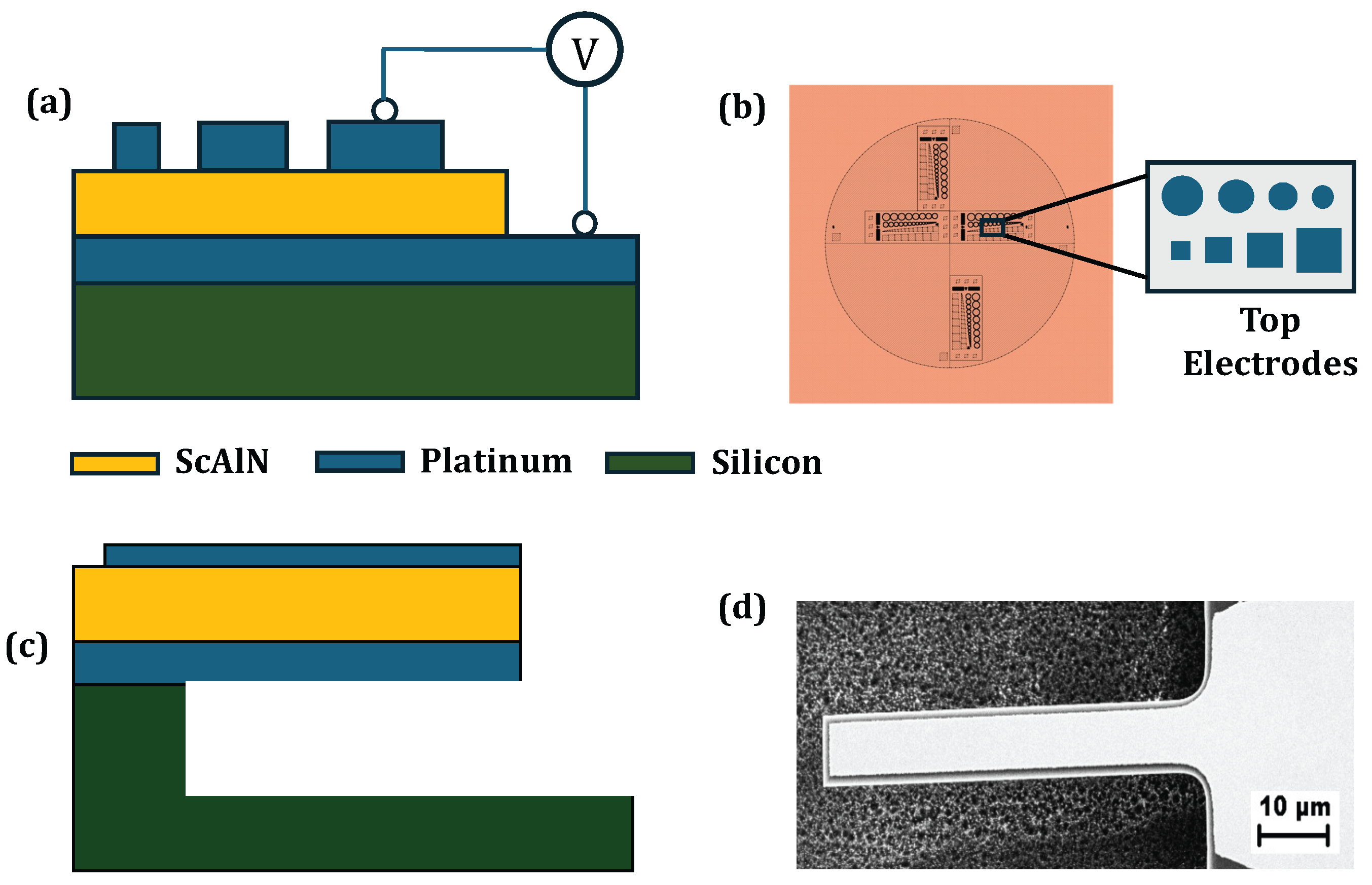
Figure 2.
Stress dependence with the process parameters: (a) flow rate, (b) Chuck height, (c) Temperature, and (d) Substrate RF Power.
Figure 2.
Stress dependence with the process parameters: (a) flow rate, (b) Chuck height, (c) Temperature, and (d) Substrate RF Power.
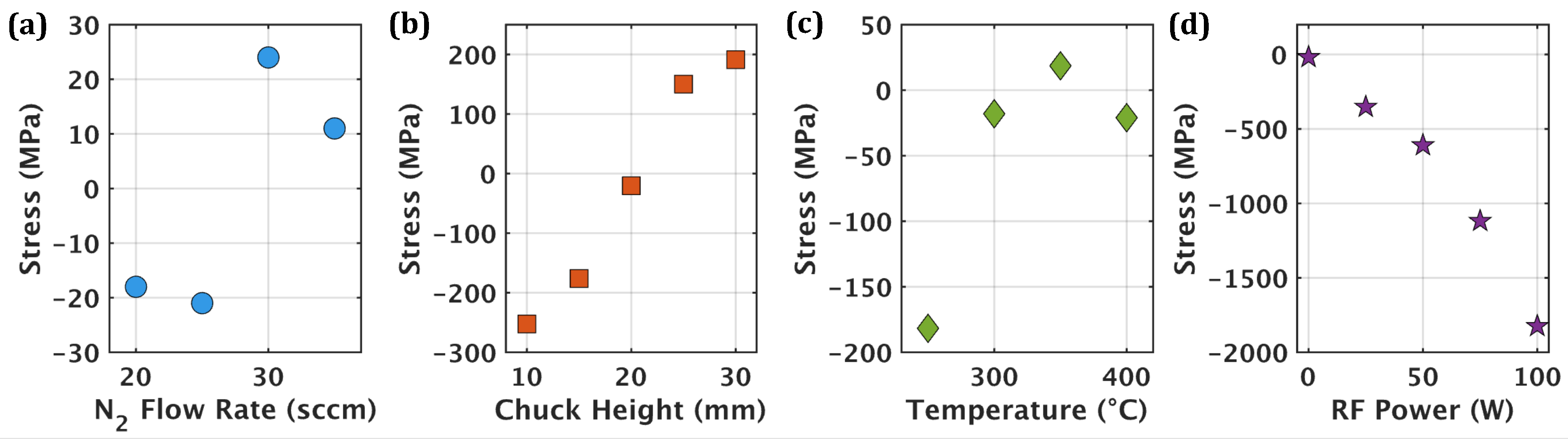
Figure 3.
Dependence of crystalline structure on process parameters: (a) Flow Rate, (b) Chuck Height, (c) Temperature, and crystalline quality on (d) Flow Rate, (e) Chuck Height, (f) Temperature.
Figure 3.
Dependence of crystalline structure on process parameters: (a) Flow Rate, (b) Chuck Height, (c) Temperature, and crystalline quality on (d) Flow Rate, (e) Chuck Height, (f) Temperature.
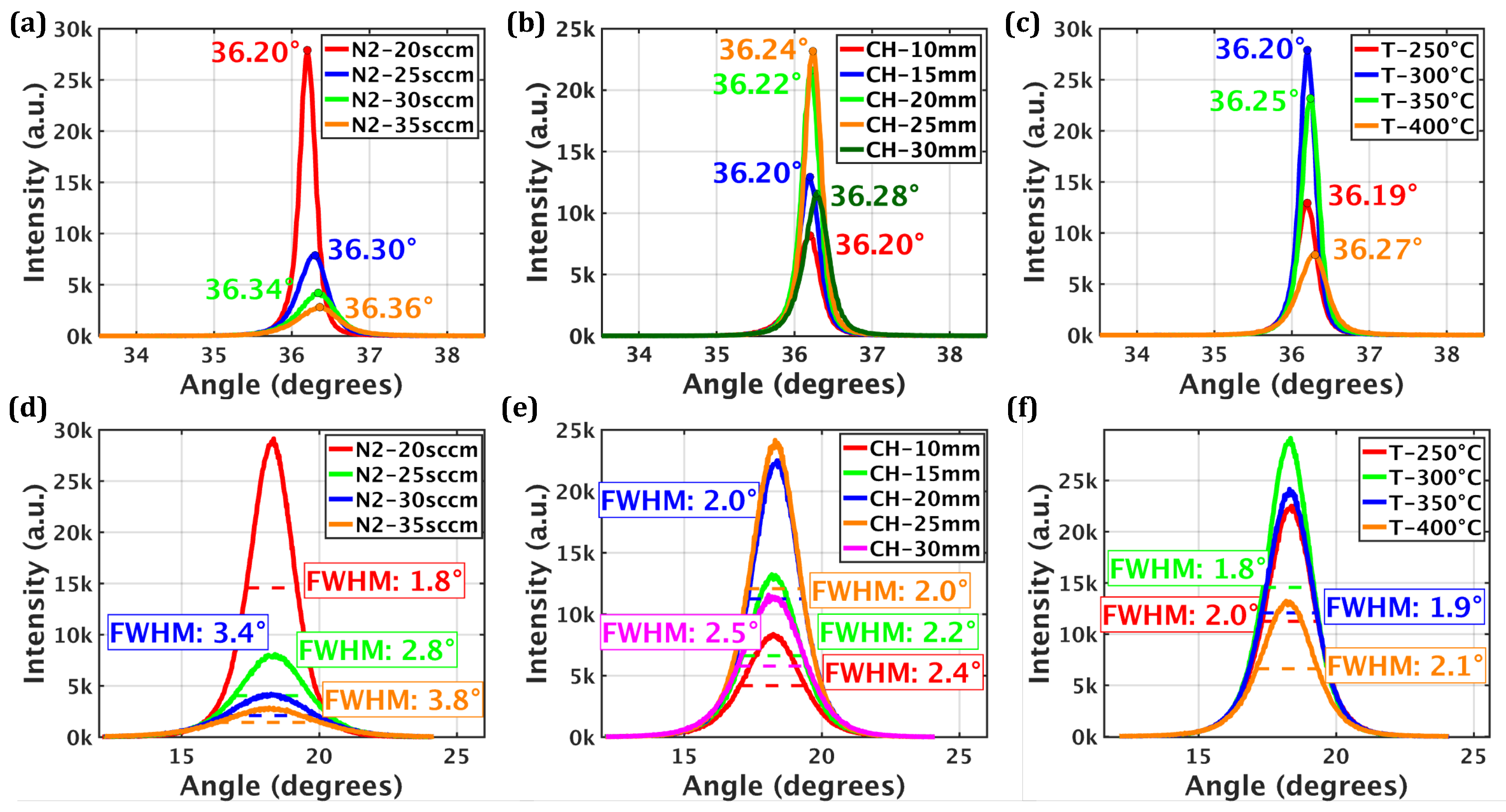
Figure 4.
(a) a broad 2 scan on ScAlN sample deposited on Si/Pt substrate, (b) rocking curve comparison between ScAlN samples deposited on different sized substrates.
Figure 4.
(a) a broad 2 scan on ScAlN sample deposited on Si/Pt substrate, (b) rocking curve comparison between ScAlN samples deposited on different sized substrates.
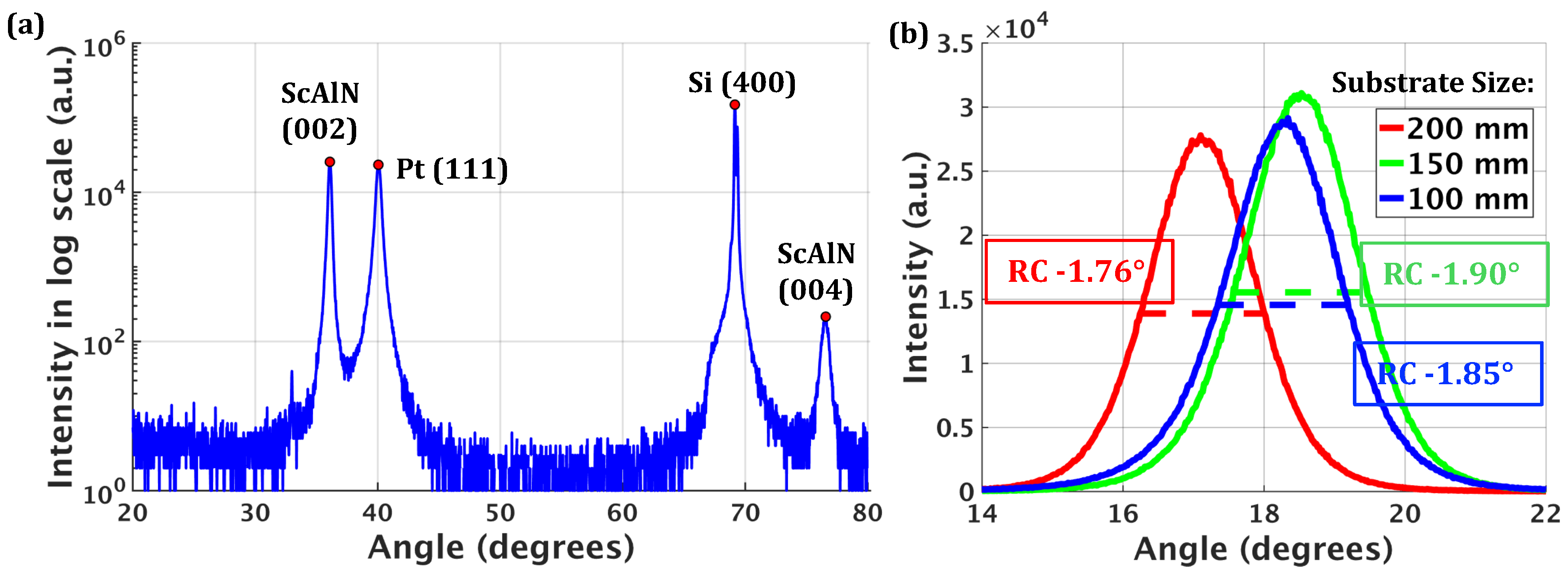
Figure 5.
(a) Formation of AOG’s on ScAlN film surface, (b) Transformation of the SEM image to extract AOG pixel count; AOG Probability Density at different (c) Flow Rates, (d) Chuck Height, (e) Temperature, and (f) substrate RF Power.
Figure 5.
(a) Formation of AOG’s on ScAlN film surface, (b) Transformation of the SEM image to extract AOG pixel count; AOG Probability Density at different (c) Flow Rates, (d) Chuck Height, (e) Temperature, and (f) substrate RF Power.
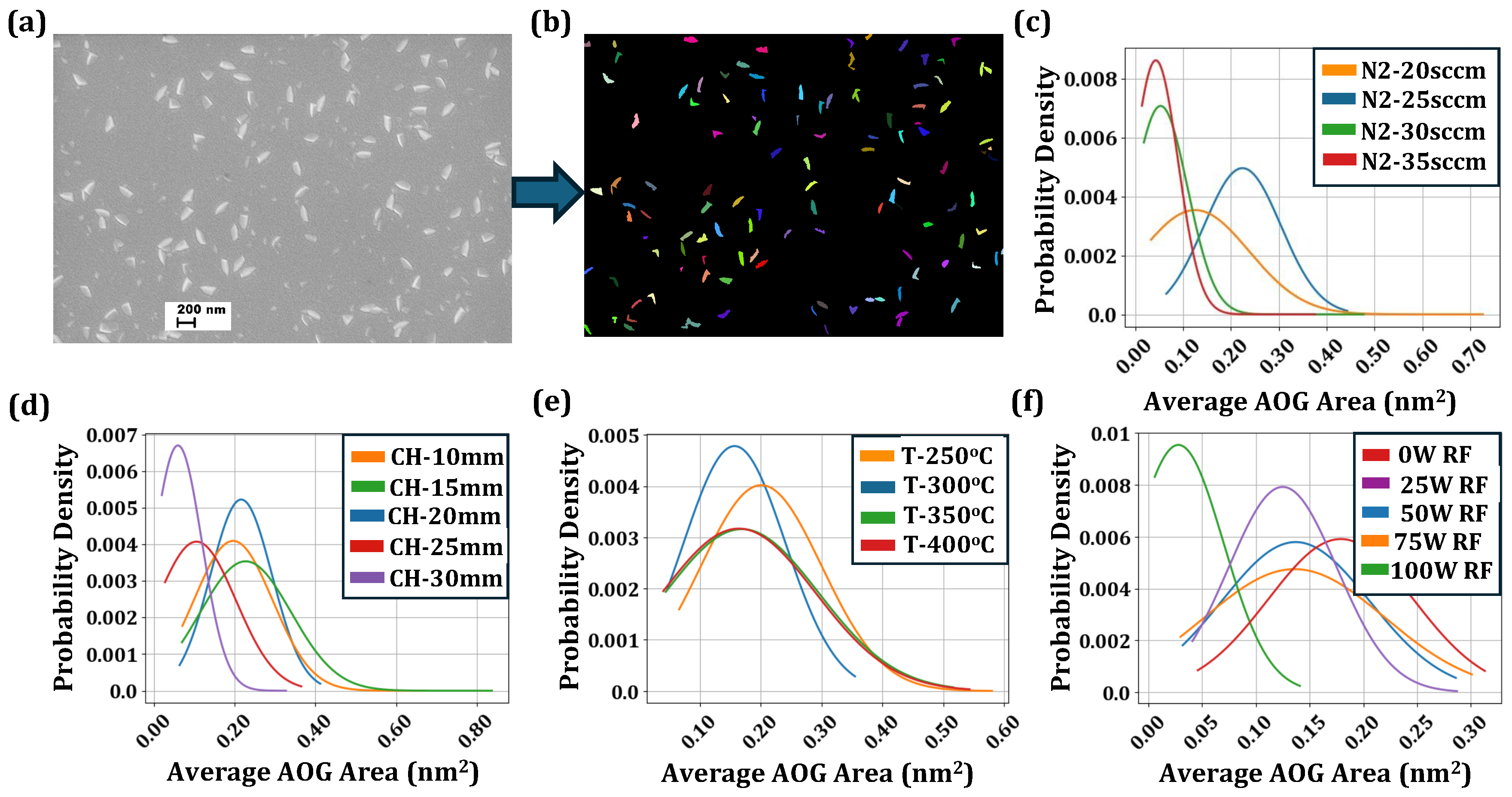
Figure 6.
Top surface view from AFM, (a) breaking vacuum and, (b) without breaking vacuum, (c) deposited at lower temperature breaking vacuum.
Figure 6.
Top surface view from AFM, (a) breaking vacuum and, (b) without breaking vacuum, (c) deposited at lower temperature breaking vacuum.
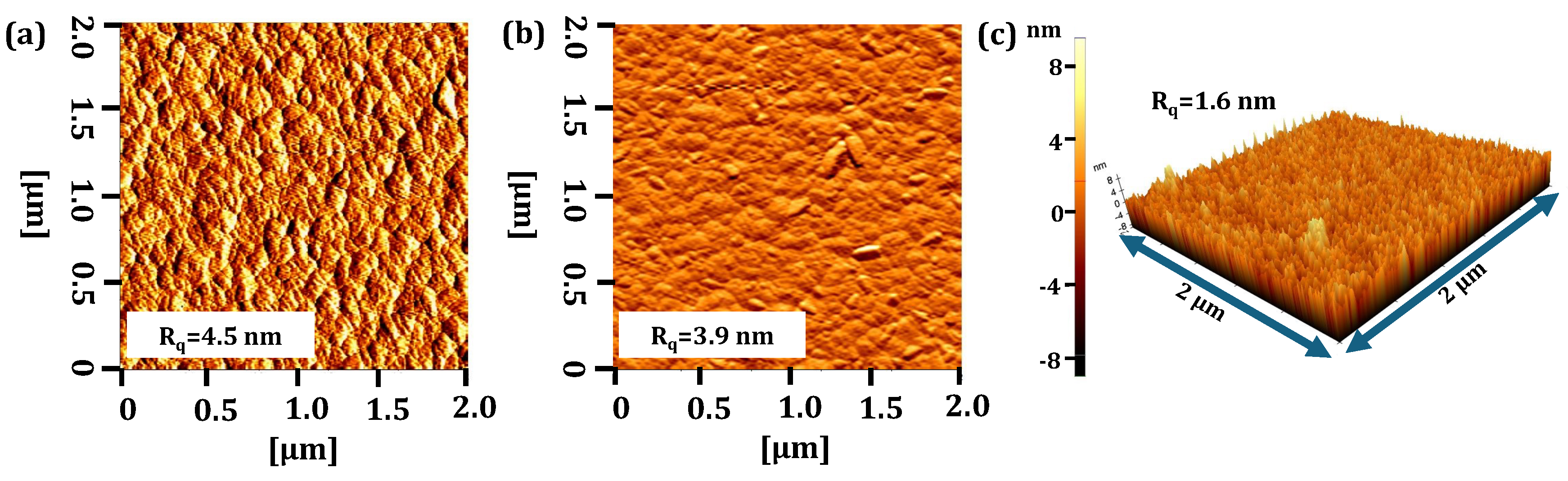
Figure 7.
Variation of piezoelectric and dielectric properties: (a) , (b) and, (c) with different substrate sizes, (d) displacement of the cantilever with the applied voltage vias and, (e) variation with the cantilever length to width ratio.
Figure 7.
Variation of piezoelectric and dielectric properties: (a) , (b) and, (c) with different substrate sizes, (d) displacement of the cantilever with the applied voltage vias and, (e) variation with the cantilever length to width ratio.
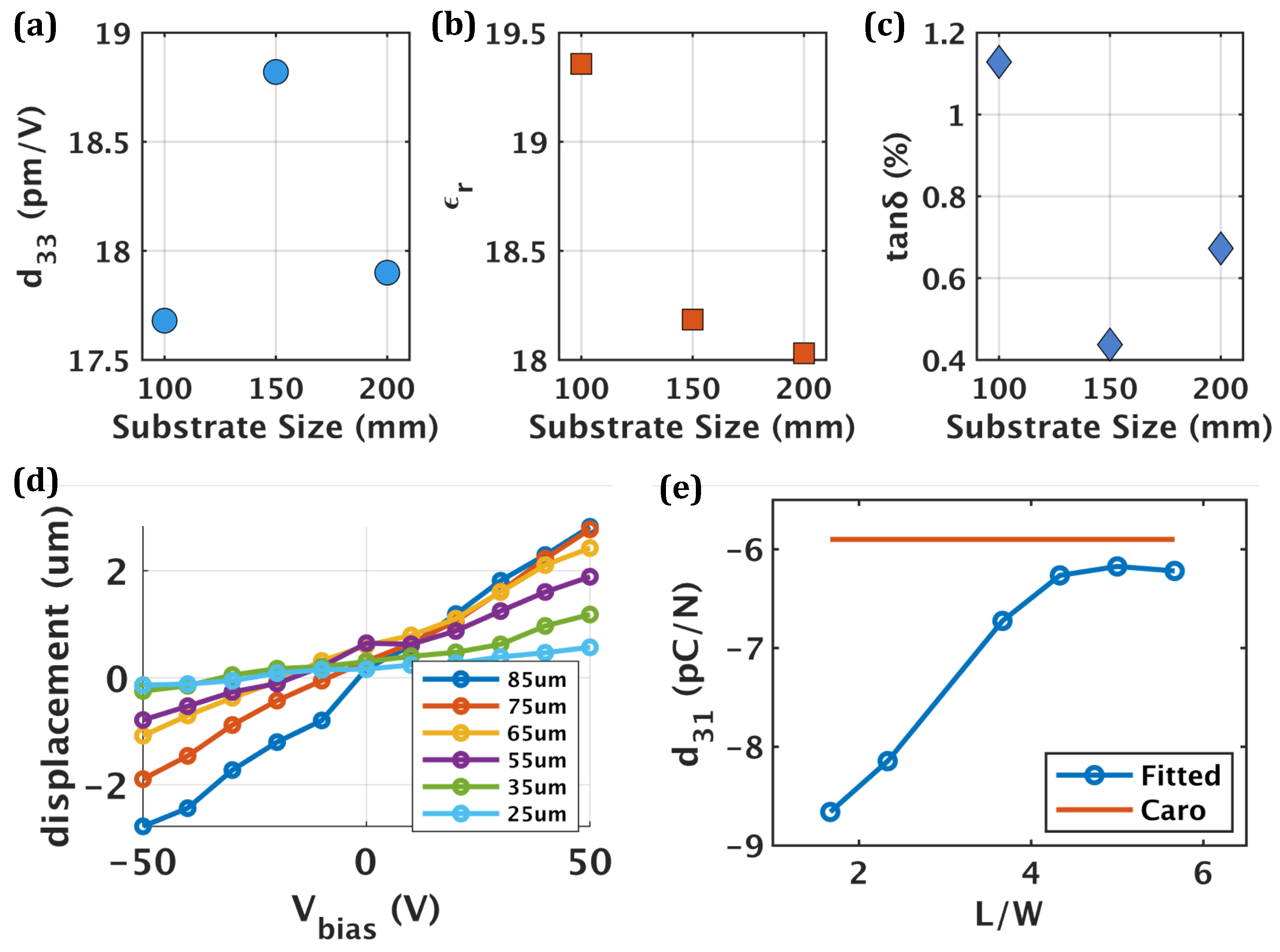
Figure 8.
Voltage-displacement plot from Piezoelectric measurement (a) under coercive field (Ec), (b) over coercive field (Ec) (butterfly curve) (c) Polarization-current loop with respect to applied electric field from DHM measurement, and (d) switching current peaks from PUND measurement.
Figure 8.
Voltage-displacement plot from Piezoelectric measurement (a) under coercive field (Ec), (b) over coercive field (Ec) (butterfly curve) (c) Polarization-current loop with respect to applied electric field from DHM measurement, and (d) switching current peaks from PUND measurement.
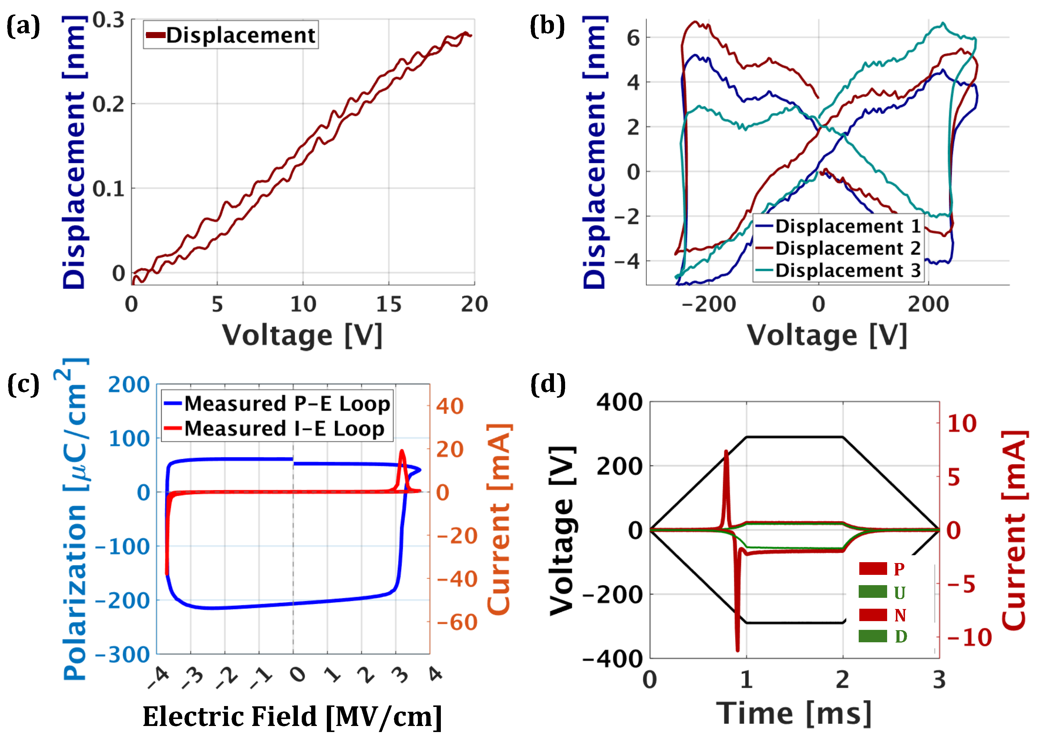

Table 1.
Deposition parameters window−explored for ScAlN thin film process optimization.
| Parameter | Optimum Value | Range Investigated |
|---|---|---|
| N2 flow rate (sccm) | 20 | 20 − 35 (step 5) |
| Chuck height (mm) | 20 | 10 − 30 (step 5) |
| Temperature (°C) | 300 | 250 − 400 (step 50) |
| Target power (kW) | 5 | − |
| Substrate RF power (W) | 0 | 0 − 100 (step 25) |
Table 2.
Comparison table for piezoelectric ( , ), dielectric (, ), and ferroelectric (, ) responses for different piezoelectric materials to state-of-the-art.
Table 2.
Comparison table for piezoelectric ( , ), dielectric (, ), and ferroelectric (, ) responses for different piezoelectric materials to state-of-the-art.
| Film | Piezoelectric [, ] | Dielectric [avg. , min. ] | Ferroelectric [, ] | FOM |
|---|---|---|---|---|
| Sc0.3Al0.7N[This work] | 18 pm/V, pC/N | 18, 0.4% | 3.5 MV/cm,260 C/cm2 | 5.4 |
| AlN [61] | 5.15 pm/V, pm/V | 10.2, 0.1% | −, − | 6.6 |
| PZT[62] | − , pm/V | 935, 3.6% | −, − | 3.6 |
| PZT[63] | 26.4 pm/V,− | 1026, 2.5% | 0.052 MV/cm,17 C/cm2 | − |
| HZO[64] | 26.4 pm/V,− | 42, − | 0.75 MV/cm,24 C/cm2 | − |
| AlScBN[65] | 25 pm/V,− | −, − | 2.0 MV/cm,140 C/cm2 | − |
Disclaimer/Publisher’s Note: The statements, opinions and data contained in all publications are solely those of the individual author(s) and contributor(s) and not of MDPI and/or the editor(s). MDPI and/or the editor(s) disclaim responsibility for any injury to people or property resulting from any ideas, methods, instructions or products referred to in the content. |
© 2026 by the authors. Licensee MDPI, Basel, Switzerland. This article is an open access article distributed under the terms and conditions of the Creative Commons Attribution (CC BY) license (http://creativecommons.org/licenses/by/4.0/).
Copyright: This open access article is published under a Creative Commons CC BY 4.0 license, which permit the free download, distribution, and reuse, provided that the author and preprint are cited in any reuse.


