Submitted:
09 January 2026
Posted:
12 January 2026
You are already at the latest version
Abstract
The exploration of probabilistic computing has recently gained momentum as a promising par-adigm to overcome the limitations of deterministic CMOS logic. In this paper, we present an FPGA-based digital emulator of probabilistic bits (p-bits) and stochastic logic circuits introducing three key innovations. First, we implement p-bits with a sigmoidal activation function, enabling faithful emulation of spin-inspired probabilistic logic while preserving the statistical character-istics of physical p-bit devices. Second, we eliminate the need for the sequencer—commonly re-quired in weighted p-bit architectures to sequentially activate each unit and ensure stability—by demonstrating, through quantitative metrics that our fully parallel design achieves stable and reproducible behavior. Third, we propose a reusable and parameterized hardware library of elementary probabilistic components, implemented as modular Verilog HDL blocks that provide a robust foundation for the construction of more complex stochastic systems, including Boltzmann machines, probabilistic SAT solvers, stochastic optimization architectures, and binary neural networks. With the proposed approach, we designed and emulated on Altera/Intel FPGAs using the Quartus Prime Integrated Development Environment (IDE) a wide set of probabilistic logic gates and probabilistic digital systems up to finite state machines (FSMs), achieving excellent results in terms of both accuracy and stability of the outcomes. The proposed FPGA-based archi-tecture thus serves both as a research instrument for investigating probabilistic computation and as a practical platform for scalable hardware accelerators in emerging stochastic applications.
Keywords:
probabilistic computing
; p-bit
; FPGA emulation
; spin logic
; stochastic circuits
; Boltzmann machines
; hardware accelerators
1. Introduction
The search for computing paradigms beyond CMOS has intensified in recent years, driven by the scaling limitations and energy constraints of conventional digital electronics. Among the most promising alternatives, probabilistic spin logic (PSL), based on probabilistic bits (p-bits), has attracted significant attention [1,2]. A p-bit is a binary stochastic unit [3,4] whose state fluctuates between 0 and 1 with probabilities governed by an activation function. The probability of the i-th p-bit being in state 1 is typically expressed as:
where: σ is the activation function, Ii is the input signal, kB is the Boltzmann constant, and T represents an effective temperature [5].
This stochastic behavior provides a natural substrate for Boltzmann-machine dynamics [6,7], enabling efficient sampling, probabilistic inference, and stochastic optimization. Unlike deterministic Boolean logic, where bits take fixed values and computations follow rigid truth tables [8], p-bit-based electronics exploit randomness as a computational resource [9,10]. Such an approach offers several advantages, including the ability to tackle NP-hard optimization problems through probabilistic sampling [11,12], robustness to device variability and environmental noise [13], and support for in-memory computation that helps alleviate the von Neumann bottleneck [14].
Networks of p-bits have been applied to combinatorial optimization (e.g., traveling salesman and maximum cut) [15,16], machine learning through Boltzmann machines and generative models [17,18], Bayesian inference, Monte Carlo sampling, and stochastic optimization [19,20]. Additional emerging domains include neuromorphic computing, where stochastic switching resembles neural spiking [21], and quantum-inspired computation, where classical probabilistic dynamics emulate specific classes of quantum Hamiltonians using classical stochastic hardware [22].
The efficient realization of these architectures on reconfigurable hardware platforms such as Field-Programmable Gate Arrays (FPGAs) represents a key step toward dedicated emulators and accelerators for probabilistic computing. Several FPGA implementations of p-bits and stochastic circuits have been reported, notably the weighted p-bit architecture introduced by Pervaiz et al. [23]. These intrinsically probabilistic units integrate randomness with local memory and demonstrate the feasibility of scalable hardware realizations. However, they also highlight critical limitations: stability requires sequential activation via a centralized sequencer, modularity is limited, and scalability is constrained by architectural complexity.
In parallel, within neural network research, the sigmoid function is widely employed as an activation function that maps a linear input to a probability value between 0 and 1, especially in binary classification tasks. Although neural networks are often interpreted probabilistically, they are not intrinsically probabilistic models in the same sense as Probabilistic Spin Logic (PSL). This distinction motivates the exploration of sigmoid-based probabilistic hardware that preserves the formal probabilistic semantics of p-bits.
This paper proposes a new FPGA-based implementation of p-bits using a sigmoidal activation function, designed to emulate PSL efficiently and reproducibly. The contributions of this work are threefold: (i) introducing sigmoid-activated p-bits as an alternative to weighted p-bits, enabling direct emulation of spin-inspired logic; (ii) demonstrating that fully parallel updates—without any sequencer—still achieve stable and accurate behavior, validated through quantitative metrics; and (iii) presenting a parameterized hardware library of probabilistic components suitable for building scalable architectures including Boltzmann machines, SAT solvers, stochastic optimizers, and binary neural networks.
Using this framework, a set of fundamental probabilistic circuits—such as logic gates (XOR, AND, OR, NOT), a generic Boolean network, a full adder, a majority circuit, a memory cell, a counter, and a finite state machine—has been implemented on an Intel/Altera FPGA using the Quartus Prime environment. The design is fully described in Verilog HDL and is therefore portable across FPGA vendors and toolchains. A MATLAB double-precision simulator is also provided as a software reference for validation.
The remainder of this paper is organized as follows. Section 2 reviews the theoretical foundations of probabilistic bits and FPGA-based emulation of probabilistic spin logic. Section 3 describes the proposed method, including the sigmoid-based p-bit architecture and the associated Verilog HDL library. Section 4 presents the experimental results obtained from MATLAB simulations and FPGA-based emulation, covering a range of probabilistic logic, arithmetic, and sequential circuits. Section 5 discusses the results, highlighting architectural trade-offs and comparisons with existing p-bit implementations. Finally, Section 6 concludes the paper and outlines perspectives for future probabilistic hardware systems.
2. Overview and Theoretical Background on p-bit Emulation
Probabilistic computing represents a new paradigm that uses intrinsic randomness to solve otherwise intractable computational problems. A crucial step toward its practical realization is the emulation of probabilistic behavior on conventional reconfigurable hardware platforms, particularly FPGAs.
In the following subsections, the relevance of FPGA-based emulation is examined, followed by a review of the methodologies currently available for implementing p-bits and probabilistic circuits on FPGA. This discussion provides the foundation for highlighting the distinctive features and advantages of the proposed approach.
2.1. Importance of FPGA-Based p-bit Emulation
FPGAs provide fine-grained logic and interconnection resources, enabling the design of customized computing architectures tailored to specific applications [24,25]. Their reconfigurable nature, consisting of configurable logic blocks, interconnects, and I/O elements, makes them particularly well suited for mapping p-bits and probabilistic logic circuits into hardware.
FPGA-based emulation of p-bits plays a critical role as an intermediate step before committing to nanoscale realizations, such as spintronic devices. This approach offers several advantages. First, FPGAs provide a flexible platform for exploring different network topologies and scaling behaviors without the cost and delays associated with fabricating physical prototypes [26]. Second, FPGA emulation enables reproducible and controllable stochastic dynamics, unlike physical nanoscale devices, which often suffer from fabrication variability and environmental sensitivity [2]. Third, FPGA-based platforms facilitate hybrid architectures in which probabilistic accelerators can be seamlessly integrated with conventional digital processors [27].
Compared to software simulations, FPGA emulation also provides significant benefits. While simulations on CPUs or high-level environments such as MATLAB can reproduce stochastic behavior, they remain inherently sequential and computationally expensive when dealing with large interconnected networks [28,29]. By contrast, FPGA hardware supports true parallelism, allowing multiple p-bits to update simultaneously and thereby more faithfully reflecting the parallel nature of probabilistic spin logic [30]. This parallelism results in substantial speedups, improved scalability, and even real-time operation capabilities. Moreover, FPGA hardware guarantees predictable timing behavior, whereas software simulations are often affected by operating system overheads and variable execution times [31].
Although GPUs and microcontrollers represent alternative hardware options, FPGAs retain distinctive advantages. General-purpose CPUs and microcontrollers are inherently sequential and thus unsuitable for large-scale stochastic networks [32], while GPUs—optimized for Single Instruction Multiple Data (SIMD) floating-point operations—suffer from scheduling overheads and non-deterministic timing [33,34]. By contrast, FPGAs combine low-latency deterministic execution with massive parallelism and customizable logic, resulting in superior scalability and energy efficiency [35,36].
Table 1 summarizes the main architectural differences across these platforms.
Beyond their role as research emulators, FPGA-based p-bit systems are increasingly being recognized as practical probabilistic accelerators. Their intrinsic parallelism and energy efficiency make them particularly attractive for accelerating Monte Carlo simulations, Bayesian inference engines, and combinatorial optimization tasks [4,37,38]. The reconfigurability of FPGAs further enables adaptation to changing problem instances, outperforming fixed-function accelerators in terms of versatility [39,40]. As FPGA technology continues to advance in density, efficiency, and connectivity, its role in probabilistic hardware computing will only become more prominent [41].
A particularly promising direction is the hybrid CPU–FPGA architecture, where the CPU manages orchestration and preprocessing, while the FPGA performs the computationally intensive probabilistic updates using p-bit networks. In this division of labor, inference tasks are dispatched from the CPU to the FPGA accelerator, which returns probabilistic decisions or updated states. Such architectures enable real-time inference, scalability, and adaptability across a wide range of applications, from Bayesian reasoning and constraint satisfaction to neuromorphic computing.
2.2. State-of-the-Art FPGA-Based p-bit Implementation Methodologies and Original Contribution
Several methodologies have been proposed for implementing p-bits on FPGA platforms, each presenting specific advantages and trade-offs [42,43]. The most common strategy relies on Linear Feedback Shift Register (LFSR)-based pseudo-random number generators combined with comparison logic, where stochastic outputs are generated by comparing random values against input-dependent thresholds [44]. This approach provides efficient hardware utilization and good control over output probabilities, while maintaining computational simplicity.
Alternative solutions employ true random number generators (TRNGs), exploiting metastability in flip-flops or entropy sources such as ring oscillators to achieve genuine stochasticity [45,46]. While these implementations improve the statistical quality of randomness, they typically require additional resources and careful calibration to ensure robustness against process, voltage, and temperature variations. Hybrid approaches combine deterministic and stochastic elements, for example using lookup tables (LUTs) to realize p-bit activation functions while leveraging hardware RNGs for probabilistic decision-making [47]. More advanced implementations incorporate adaptive mechanisms, such as dynamic threshold adjustment and coupling strength modulation, to enable online learning and optimization [48].
Recent studies have also explored specialized architectures—including bistable ring networks, coupled oscillators, and magnetic tunnel junction emulators—that aim to replicate the physical dynamics of nanoscale p-bit devices more faithfully [49,50]. Indeed, most FPGA-based emulation efforts are conceptually inspired by physical devices proposed for hardware-level realization of p-bits [51,52,53,54,55]. Although a detailed review of these physical implementations lies beyond the scope of this paper, it is worth noting the class of quasi-zero energy barrier probabilistic devices, which intrinsically realize sigmoid activation functions [22]. This concept is closely related to the methodology adopted in this work and will be further described in the following sections.
A key milestone in the literature is the introduction of weighted p-bits, which are strongly oriented to FPGA implementation and provide significant advantages compared to stream-based methods in terms of scalability, resource efficiency, and statistical accuracy. Weighted p-bits are stochastic computational units fluctuating between binary states (0 and 1), with tunable probabilities modulated by external inputs. Beyond Bayesian inference, their applications extend to combinatorial optimization (e.g., Traveling Salesman Problem, Max-Cut), stochastic machine learning models such as Restricted Boltzmann Machines and Deep Belief Networks, physical simulations including the Ising model, and cryptographic systems requiring secure random number generation. This versatility makes weighted p-bits a promising substrate for probabilistic hardware computing.
The paradigm of encoding probabilities as digital weights rather than continuous bitstreams was primarily advanced by researchers at Purdue University, who demonstrated its superiority over traditional schemes requiring one RNG per p-bit. The foundational work by Pervaiz et al. [23] formally introduced weighted p-bits for scalable FPGA-based probabilistic circuits (p-circuits). Their contribution, later contextualized and reinforced by the broader architectural vision of interconnected p-units described by Camsari et al. [5], represents the current state of the art. A critical analysis of these two works highlights both the strengths and the limitations of the weighted p-bit methodology.
These pioneering designs emulate networks of stochastic binary units whose state is updated according to a tunable sigmoid probability, implementing the relation
where approximates the thermal activation of low-barrier nanomagnets. In such systems, weighted interconnections are realized through analog-inspired multipliers or digital matrix operations, and sequential updating of the p-bit array is typically enforced by a sequencer to maintain the statistical correctness of the Markov chain.
The first major strength lies in scalability and resource efficiency. In conventional implementations, each p-bit requires a dedicated LFSR, making large-scale systems impractical. Pervaiz et al. [23] solved this bottleneck by decoupling probabilistic logic from random number generation: a p-bit’s probability is stored as a digital weight, while interactions are computed deterministically through arithmetic operations. This reduces the need for multiple RNGs, as a single, high-quality generator can be shared across the system. Camsari et al. [5] further support this perspective, positioning p-bits as efficient, interconnected probabilistic units.
The second strength is computational efficiency. By representing weights and probabilities as digital values, the stochastic update process becomes a weighted summation followed by an activation function, operations well suited for FPGA parallelism and pipelining. This yields significant speedups compared to traditional bitstream-based stochastic computing.
Architecturally, the design proposed in [23] separates the p-bit into two functional blocks: (i) a deterministic weight matrix, which computes activation values via summations and multiplications; and (ii) a tunable RNG block, containing the LFSR, which maps the activation value to a probability threshold and produces the stochastic output by comparison. Crucially, the RNG block can be shared among multiple p-bits, eliminating the one-to-one mapping of LFSRs to p-bits and thereby achieving scalability. In this model, the LFSR is still present but relegated to a centralized, reusable resource, while the defining elements of the p-bit are its weights and arithmetic logic.
Despite these advantages, both works [5,23] reveal important limitations. First, stability of stochastic dynamics still requires a sequencer to enforce sequential updates, an approach inherited from Boltzmann machine theory. Second, activation functions are restricted, with limited flexibility and reduced interpretability for neuromorphic applications. These gaps define the scope for the original contributions of the present paper.
More recent works have focused on digital emulation on FPGA platforms, emphasizing area–latency efficiency and scalability. Sigmoid approximations have evolved from look-up-table (LUT) implementations to piecewise linear or rational polynomial forms optimized for low resource usage and low latency [56,57,58]. Notably, the authors in [56] demonstrated a curvature-adaptive piecewise linear method providing a 40% reduction in logic utilization with negligible error, while in [57] introduced a Taylor-segment approach achieving 11-bit accuracy with minimal DSP cost. Such techniques are directly applicable to p-bit emulators in which the sigmoid serves as the activation core.
The random excitation required by stochastic neurons is typically generated through pseudo-random number generators (PRNGs) such as LFSRs or through true random number generators (TRNGs) exploiting metastability or oscillator jitter [45,46,59]. TRNG-based approaches (e.g., Fibonacci–Galois ring oscillators or start–stop phase-detuned rings) offer higher entropy at the cost of reduced controllability, whereas PRNG-based methods provide deterministic reproducibility, desirable for debugging and FPGA verification.
An important architectural aspect in the literature is the update scheduling of p-bits. Sequential updates are used in the weighted p-bit models to guarantee convergence to the intended Boltzmann distribution. However, several FPGA implementations inspired by Ising machines and Restricted Boltzmann Machines (RBMs) have demonstrated that parallel or block-parallel updates can still yield correct and stable solutions for optimization tasks [60,61,62]. Recent studies on hardware Ising annealers implemented via Hamiltonian Monte Carlo also report negligible degradation in accuracy under synchronous updates, while drastically improving throughput. These findings align with the results obtained in the present work, where sequencer-free parallel updates maintain statistical stability and deterministic convergence across multiple probabilistic logic designs.
Table 2 summarizes the key design trade-offs in FPGA-based p-bit emulation, highlighting how the choice of activation function, randomness source, and update scheduling affects hardware complexity, statistical fidelity, and scalability.
The recent literature on hardware-efficient sigmoid implementations, such as the works in [56] and [57], has confirmed the practicality and accuracy of LUT-based and piecewise-linear approximations for digital hardware. These studies, primarily targeting neural and machine learning applications, demonstrate that the sigmoid function can be efficiently realized on FPGA with minimal resource overhead while preserving numerical stability. In this work, the same class of techniques is repurposed within a spin-inspired probabilistic computing framework, where the sigmoid serves as the stochastic activation core of each p-bit. This choice establishes a methodological bridge between neural hardware accelerators and probabilistic spin logic, providing both physical interpretability and hardware efficiency.
Building on this foundation, the proposed architecture introduces several original contributions that extend beyond the current state of the art.
The first original contribution is the introduction of a parameterized Verilog HDL p-bit cell, conceived as a modular and reusable hardware element. Unlike previous proof-of-concept implementations of individual gates and circuits [5,23], the proposed cell provides configurable parameters for weights, thresholds, and activation functions. This parameterized framework enables the systematic construction of probabilistic logic gates (AND, OR, XOR), registers, counters, adders, finite-state machines, and higher-level stochastic systems using the same unified building block. Such modularity promotes standardization, accelerates development, and ensures portability across FPGA families. Moreover, it approximates the notion of a functionally complete probabilistic system, analogous to the universal NAND or NOR gates of classical logic, thereby allowing the synthesis of any probabilistic digital circuit through parameter adjustment [63,64].
The second original contribution concerns the adoption of a sigmoid-based activation function in place of the weighted scheme. Inspired by recent studies on near-zero energy barrier probabilistic devices that intrinsically realize sigmoid dynamics [22], as well as FPGA-oriented research on hardware-efficient approximations of the sigmoid function (e.g., LUT-based, piecewise linear, or Taylor-segment implementations) [56,57,58], this design offers more direct control and clearer physical interpretability of model parameters such as interaction strength and bias. Compared with the weighted p-bit framework, the proposed LUT-based sigmoid realization provides greater flexibility, higher numerical stability, and closer alignment with spin-based probabilistic models, while remaining fully compatible with FPGA resources such as LFSRs for randomness generation.
The third contribution is the elimination of sequencers, a major architectural simplification. Whereas the weighted p-bit framework requires sequential updates to preserve the statistical correctness of the Markov chain [23], the proposed parameterized, sigmoid-based p-bits achieve stable and accurate stochastic behavior under fully parallel operation. This is validated by dedicated evaluation metrics demonstrating consistent statistical behavior without temporal control circuitry. Removing sequencers reduces design complexity, enhances throughput, and substantially improves scalability.
In summary, the proposed FPGA framework builds upon the foundation established by Pervaiz et al. [23] and Camsari et al. [5], while drawing methodological inspiration from more recent advances in hardware-efficient sigmoid realizations on FPGA, such as those reported in [56] and [57]. The present work overcomes the key limitations of the weighted p-bit framework by introducing (i) a parameterized p-bit library for modular and reusable design, (ii) a hardware-optimized sigmoid activation function—consistent with proven FPGA-efficient techniques yet applied here within a spin-inspired probabilistic computing paradigm—and (iii) a sequencer-free architecture enabling fully parallel stochastic operation.
Together, these innovations establish a unified, physically interpretable, and resource-efficient approach to probabilistic computation. They simplify the hardware design flow, improve system scalability, and pave the way for more versatile FPGA-based emulators of spin-inspired probabilistic logic circuits.
In contrast to prior FPGA-based p-bit implementations that primarily target faithful emulation of Boltzmann-machine dynamics, the present work emphasizes architectural simplicity, modularity, and deterministic reproducibility, positioning the proposed framework as a practical engineering platform for probabilistic logic and sequential stochastic systems.
3. Method
This section describes the methodology adopted to implement the proposed FPGA-based emulator of spin-inspired probabilistic logic. The approach emphasizes three main contributions of this work:
- (i)
- the realization of a sigmoid-activated p-bit,
- (ii)
- a parameterized hardware design enabling reusability and scalability, and
- (iii)
- the elimination of the sequencer, made possible by the intrinsic stability of the proposed architecture and validated through quantitative metrics.
To illustrate the methodology concretely, the design of a probabilistic XOR gate is used as a representative case study. The same architectural principles and design rules are subsequently applied to other probabilistic logic circuits and systems.
3.1. Sigmoid-Based p-bit Implementation
As discussed in Section 2, p-bits are stochastic computational units that fluctuate between binary states according to a probability distribution governed by external inputs. In this work, the intrinsic probabilistic behavior of p-bits is digitally emulated through the combination of a sigmoid activation function and a pseudo-random number generator implemented on FPGA hardware.
Figure 1 depicts the block diagram of the proposed sigmoid-activated p-bit.
The core computational flow consists of four main stages: input scaling, value clipping, sigmoid approximation, and stochastic comparison. In the first stage, the interaction signal—analogous to the local field in spin models—is scaled according to equation (3)
I_scaled = I₀ × interaction + BIAS
Here, I₀ and BIAS are configurable parameters represented in Q9 fixed-point format (i.e., 9 fractional bits, corresponding to a scaling factor of 512). This operation maps the interaction term into the appropriate numerical range for subsequent sigmoid evaluation.
In the second stage, value clipping constrains I_scaled to the interval [−1024, +1024], corresponding to the normalized range [−2.0, +2.0] in real-valued units. This clipping prevents numerical overflow and ensures that the input to the sigmoid function remains within the domain covered by the lookup table.
In the third stage, the clipped value of I_scaled is normalized and mapped to a 512-entry sigmoid lookup table through uniform quantization of the input range, and the sigmoid activation function is evaluated to produce a probability value p ∈ [0,1]. The LUT-based implementation significantly reduces computational complexity compared to direct sigmoid evaluation, making the design suitable for resource-constrained FPGA architectures.
The sigmoid function is defined as:
σ(I_scaled) = 1/(1 + e^((-I_scaled)/512))
Here, I_scaled is represented in Q9 fixed-point format, and the division by 512 converts the fixed-point value into its real-valued equivalent prior to exponential evaluation.
It is worth noting that, while Equation (4) describes the functional form of the sigmoid activation, the effective slope (or temperature) of the response is determined by the specific parametrization of the lookup table. In the proposed implementation, the sigmoid LUT implicitly incorporates a reduced effective temperature, yielding a steeper activation profile that enhances stability for logic-oriented probabilistic circuits. This approach is consistent with the general p-bit formulation, where the ratio I/(kBT) governs the stochastic behavior.
In the final stage, a pseudo-random number generated by a Linear Feedback Shift Register (LFSR), implemented in Verilog HDL within the lfsr.v module, is compared with the probability p obtained from the sigmoid activation. The p-bit output is set to 1 if rand_num < p, and to 0 otherwise, effectively implementing a Bernoulli random variable with parameter p. This mechanism enables each p-bit to act as an autonomous probabilistic computing element.
Figure 2 provides an algorithmic representation of the p-bit cell, highlighting the correspondence between interaction computation, sigmoid activation, and stochastic sampling.
3.2. Probabilistic XOR Gate Design
To demonstrate the proposed design methodology, a probabilistic XOR gate was implemented as a representative case study. The module pbit_xor.v (Figure 3) configures the p-bit architecture to reproduce spin-glass-like probabilistic behavior corresponding to the XOR Boolean function.
Boolean inputs and are first mapped to bipolar spin variables and , taking values in Q9 fixed-point format, where logical ‘1’ corresponds to +512 and logical ‘0’ to −512. The interaction term is computed as
with BIAS = -1024 corresponding to -2.0 in Q9 representation. In practice, the interaction value is further scaled by an effective gain implicitly embedded in the sigmoid lookup table, resulting in a steeper activation profile than that of a unit-slope logistic function. This formulation ensures that identical inputs (00 or 11) yield a negative interaction, while different inputs (01 or 10) produce a positive interaction, naturally encoding the XOR logic condition.
I = BIAS - 3 × (s0 × s1),
The product s₀ × s₁ is computed in Q18 format (18 fractional bits) and right-shifted by 9 bits to restore Q9 precision. For example, when s₀ = s₁ = +512, the product yields +262144 in Q18, which becomes +512 in Q9 after the right shift. The resulting interaction signal is then fed to the p-bit module (pbit.v), where an internal BIAS equal to zero is used, as the offset is already embedded in the interaction term. The p-bit performs sigmoid activation and stochastic comparison using a 32-bit LFSR-based random generator (lfsr.v).
Table 3 summarizes the input-output behavior of the probabilistic XOR gate.
With the selected parameters, the interaction term is strongly positive (+512) when XOR = 1 and strongly negative (−1024) when XOR = 0, biasing the p-bit output toward the correct logical value while preserving controlled stochasticity. This behavior effectively emulates spin-inspired probabilistic logic with controlled randomness, suitable for neural and optimization-oriented applications.
Figure 3 illustrates the complete architecture of the probabilistic XOR gate, including spin mapping, interaction computation, random number generation, and stochastic output.
This approach differs from weighted p-bits as introduced by Pervaiz et al. [23], which require sequential updates to maintain stability. In contrast, the proposed digital implementation achieves reproducible and controllable probabilistic behavior on FPGA, providing a practical platform for emulating and prototyping spin-inspired probabilistic systems.
3.3. Parametrized p-bit Architecture
A second distinctive feature of this work, representing a key novelty, is the parameterization of both the p-bit and random number generator modules. The Verilog HDL modules (pbit.v and lfsr.v) are designed with configurable parameters including interaction scaling (), bias (BIAS), data width (DATA_WIDTH), and random generator width (RAND_WIDTH). This modular approach allows the same HDL description to be rapidly reconfigured for different probabilistic logic functions without redesign.
The parameterized framework enables reuse of the same p-bit module to construct probabilistic AND, OR, and XOR gates, as well as larger architectures such as Boltzmann machines, probabilistic SAT solvers, stochastic optimization systems, and binary neural networks. Additionally, the lfsr.v module supports user-defined seeds and widths, allowing independent noise sources to be assigned across multiple p-bits. This modularity facilitates the creation of a reusable library of probabilistic components, accelerating FPGA prototyping and supporting scalability toward complex systems.
An important advantage of the proposed approach is that the overall project structure remains identical across all applications. Each design is composed of the following elements:
- Main module (e.g., pbit_xor.v), which is application-specific and defines the interaction function and input/output mapping;
- Sigmoid-based p-bit module (pbit.v), fully parameterized and common to all designs;
- Pseudo-random number generator (lfsr.v), implementing a 32-bit LFSR and shared across projects;
- Performance monitoring module (performance_monitor.v), largely identical across implementations with minor adaptations;
- Sigmoid LUT files (sigmoid_lut.txt and sigmoid_lut.mif), containing the activation function lookup table.
In this way, the XOR gate project shares the same building blocks as all other applications, with only the main module differing to adapt the architecture to the specific probabilistic logic being emulated. This organization simplifies hardware design, enhances reusability, and ensures scalability toward more complex stochastic circuits.
3.4. Evaluation Metrics
The third contribution of this work is the demonstration that probabilistic circuits can operate correctly without a sequencer, traditionally required in weighted p-bit systems to ensure convergence of the Markov chain [23]. In the proposed implementation, sigmoid-activated and parameterized p-bits are updated fully in parallel while maintaining statistical accuracy and stability.
To quantify emulation quality, a dedicated performance monitoring module (performance_monitor.v) was developed to compute metrics online. The evaluation employs three complementary metrics:
- (i)
- Conditional Accuracy (CA): the fraction of samples in which the p-bit output matches the expected logical value, computed per input condition. CA provides a direct measure of functional correctness.
- (ii)
- Classification Error (CE): defined as CE = 1 − CA, representing the fraction of incorrect outputs. Low CE indicates reliable probabilistic logic behavior.
- (iii)
- Stability: computed as the fraction of consecutive samples in which the output remains unchanged, measuring temporal consistency. High stability indicates absence of spurious oscillations.
These metrics are computed both in the MATLAB behavioral model and in the FPGA-based ModelSim emulation through the lightweight performance_monitor module. Because these metrics are computed using identical discrete counting logic in both environments, agreement between MATLAB and FPGA results ensures that the underlying stochastic behavior is faithfully reproduced in hardware.
Additionally, the mean output value is reported for each input condition, providing a direct estimate of the output probability P(out = 1).
As discussed in Section 4, the combined analysis of these indicators confirms that the proposed FPGA emulator delivers stable and accurate probabilistic behavior even under fully parallel updates. Consequently, the sequencer can be safely omitted, reducing hardware complexity, enhancing scalability, and simplifying probabilistic circuit design.
4. Results
The methodology described in Section 3 was applied to the design and FPGA implementation of representative probabilistic circuits. MATLAB simulations serve as a double-precision reference baseline for validation, whereas the same HDL architectures were synthesized in Quartus Prime and emulated in ModelSim to assess the behavior of the FPGA-based emulator. It is important to note that MATLAB simulations serve as a behavioral reference for validating the qualitative correctness of the FPGA implementation, rather than as an exact numerical oracle. The MATLAB model employs double-precision floating-point arithmetic and a continuous sigmoid function, whereas the FPGA implementation uses Q9 fixed-point arithmetic and a 512-entry lookup table approximation. These implementation differences result in slightly different effective operating points on the sigmoid curve, leading to minor variations in absolute probability values. However, the key validation criterion is the consistency of logical behavior: both environments should produce outputs that statistically converge to the expected truth table, which is confirmed by the high Conditional Accuracy (CA > 98%) observed across all circuits in both MATLAB and ModelSim. So, the comparison between MATLAB simulations and hardware emulations highlights the accuracy, reproducibility, and stability of the proposed approach.
All circuits presented in this section share the same core modules (pbit.v, lfsr.v) and sigmoid lookup table files (sigmoid_lut.txt, sigmoid_lut.mif). Table 4 summarizes the common parameters used across all implementations. These values remain constant throughout all experiments unless explicitly stated otherwise.
All metrics are computed per input condition (e.g., 00, 01, 10, 11 for two-input gates). The performance monitoring verilog module reports Conditional Accuracy (CA), Classification Error (CE), mean output, and stability for all circuits.
Randomness is generated on-chip via the LFSR with the seed specified in Table 4. Results are fully deterministic and reproducible given identical HDL descriptions, random seeds, clock frequency, and reset protocol.
4.1. XOR Probabilistic Gate
4.1.1. Design Parameters
The XOR probabilistic gate, described in Section 3, is implemented by the pbit_xor.v wrapper, which maps Boolean inputs to bipolar spin variables and computes the interaction term as in Equation (5).
The interaction is then processed by the parameterized p-bit module (pbit.v) using a LUT-based sigmoid activation, while stochastic sampling is driven by a 32-bit LFSR (lfsr.v). Table 5 summarizes the application-specific parameters.
The interaction term follows Equation (5): I = BIAS − 3 × (s₀ × s₁), where s₀, s₁ ∈ {−512, +512} represent bipolar spin encodings of the Boolean inputs.
4.1.2. Comparative Results
Results of metrics calculated in Matlab and in ModelSim are in Table 6:
The results confirm that both MATLAB and FPGA implementations correctly reproduce the expected XOR truth table with high fidelity. MATLAB achieves CA above 98% while the FPGA implementation achieves CA consistently above 99.9%, with stability remaining above 99.9% in both cases. The higher CA observed in FPGA is attributed to the steeper sigmoid profile of the hardware LUT, which operates closer to saturation and thus exhibits more deterministic behavior. Both implementations confirm that sequencer-free operation does not compromise reliability.
4.2. AND Probabilistic Gate
The probabilistic AND gate follows the same modular structure as the XOR gate. The interaction term is defined as:
where s0 and s1 are the bipolar representations of the inputs in Q9 format. This formulation ensures that the activation probability of the p-bit is high only when both inputs are logical ‘1’.
I = s0 + s1 – 512
The implementation of the AND gate is fully consistent with the methodology introduced in Section 2 and with the XOR case discussed in Section 3.1. In both designs, the core structure relies on the same parametrized modules—namely pbit.v, implementing the sigmoid-based probabilistic unit, lfsr.v for random number generation, performance_monitor.v for metric evaluation, and the shared lookup table files (sigmoid_lut.txt, sigmoid_lut.mif). The only module that changes is the application-specific main file (pbit_and.v or pbit_xor.v), where the interaction term is defined according to the logic function under consideration.
This uniform structure highlights one of the main advantages of the proposed approach: new probabilistic circuits can be designed and emulated on FPGA simply by specifying the interaction rule and adjusting a small set of parameters, without modifying the core building blocks.
4.2.1. Design Parameters
The parameters DATA_WIDTH, I0 and BIAS are consistent with the XOR design, highlighting the reusability of the p-bit and LFSR modules across different probabilistic circuits. Only the top-level module changes, adapting the interaction computation while preserving the underlying parametrized architecture. This confirms the strength of the proposed methodology: new logic functions can be realized by simply redefining the interaction equation in the application-specific file, without modifying the core building blocks.
The parameters used to design the AND gate are summarized in Table 7:
4.2.2. Comparative Results
The results and comparisons, both for Matlab and ModelSim, are in Table 8:
As shown in Table 8, both approaches yield highly consistent results.
For input combinations corresponding to logical 0 (00, 01, 10), the mean output remains close to zero, with minor deviations in MATLAB due to the intrinsic stochastic behavior of p-bits (mean ≈0.018–0.019), while the FPGA emulator produces virtually exact values (0.000). For the case of logical 1 (11), both MATLAB and ModelSim achieve near-ideal results, with mean outputs of ≈0.981 and 1.000, respectively.
Conditional Accuracy (CA) exceeds 98% in MATLAB and reaches almost 100% in ModelSim, while Classification Error (CE) remains below 2% in all cases for MATLAB and below 0.05% in ModelSim. These results confirm that both implementations correctly reproduce the expected logical behavior, with the FPGA showing slightly higher CA due to the steeper sigmoid profile of the hardware LUT. The FPGA implementation achieves near-perfect accuracy (CA > 99.9%) with negligible classification error, demonstrating the effectiveness of the parameterized p-bit approach for implementing different logic functions.
The AND gate implementation confirms, also, that accurate and stable behavior can be achieved without resorting to sequencers, in contrast with weighted p-bit architectures [23]. This demonstrates that the proposed framework is not limited to a specific case but can be systematically extended to a broad range of probabilistic logic applications.
4.3. OR Probabilistic Gate
The OR gate introduces a positive bias to shift the activation probability toward logical OR semantics. The interaction term incorporates BIAS = +512 (corresponding to +1.0 in Q9). The implementation of the probabilistic OR gate follows the same modular design strategy adopted for the XOR and AND gates, highlighting once again the reusability and scalability of the proposed framework.
4.3.1. Design Parameters
In Table 9 the parameters for the OR gate design are listed.
4.3.2. Comparative Results
Results are summarized and compared in Table 10.
The results obtained for the probabilistic OR gate further confirm the validity of the proposed emulation framework. MATLAB simulations, considered as the reference baseline, show high conditional accuracy across all input combinations, with small classification errors in the order of 1–2% for mixed input cases (01 and 10). The outputs are stable, with mean values close to the expected logical levels (0 or 1), and the stability metrics consistently rated as excellent.
FPGA-based emulation in Modelsim exhibits even stronger performance, with conditional accuracy consistently above 99.9% and classification errors below 0.05%. The mean outputs match the expected logical values exactly, thus confirming the robustness of the stochastic hardware design.
As in the previous cases of XOR and AND gates, the consistency between MATLAB and FPGA results demonstrates the effectiveness of the parameterized p-bit approach. Notably, the introduction of the positive bias in the OR gate design (absent in XOR and AND) does not compromise accuracy nor stability, thereby reinforcing the flexibility and generality of the proposed architecture.
4.4. NOT Probabilistic Gate
The probabilistic NOT gate is implemented following the same modular approach adopted for the previous gates. The project is composed of the application-specific wrapper (pbit_not.v), the common probabilistic bit module (pbit.v), and the random number generator (lfsr.v). Additionally, the sigmoid lookup table (sigmoid_lut.txt and sigmoid_lut.mif) is used without modification.
The distinguishing feature of the NOT gate lies in the interaction definition within the wrapper: instead of summing inputs and applying a bias, as in the AND and OR gates, the NOT gate simply inverts the input signal (interaction = -s0). This inversion ensures that the output probability distribution correctly reflects the logical negation: when the input is 0, the interaction is positive and the output tends to 1; conversely, when the input is 1, the interaction becomes negative and the output tends to 0.
4.4.1. Design Parameters
The design parameters of the NOT gate are in Table 11
4.4.2. Comparative Results
Results obtained with Matlab and Quartus are summarized in Table 12
The experimental results of the probabilistic NOT gate confirm the correct functionality of the proposed design. Matlab simulations show that the gate achieves high accuracy for both input conditions, with conditional accuracy above 98% and classification error below 2%. The output distributions are well-centered around the expected values, with mout ≈ 0.98 for input 0 (corresponding to logical 1) and mout ≈ 0.02 for input 1 (corresponding to logical 0). Stability is confirmed by the low variance and standard deviation, ensuring a robust probabilistic behavior.
The hardware-level verification in ModelSim further strengthens these findings. In fact, the mean output values perfectly converge to the deterministic expectations (1.000 and 0.000), with accuracy levels above 99.9% and negligible classification error (<0.05%). The performance monitor also highlights excellent stability and accuracy.
The slightly lower stability (96%) compared to two-input gates is attributed to the simpler interaction structure, which provides less margin for noise rejection.
These results demonstrate that the probabilistic NOT gate is highly reliable and consistent across both simulation and hardware domains, maintaining the same robustness already observed for XOR, AND, and OR.
4.5. Boolean Probabilistic Network
To assess the scalability of the proposed FPGA-based p-bit emulator beyond elementary gates, a probabilistic Boolean network implementing the three-input logic function
was designed and evaluated. The network accepts three binary inputs and produces a stochastic output that statistically converges to the corresponding deterministic truth table.
f = A· B + C
4.5.1. Architecture Overview
Unlike multi-stage cascades of probabilistic gates, this implementation uses single-stage direct interaction encoding. The Boolean function is computed deterministically, and the result is encoded as an interaction field biasing a single sigmoid-activated p-bit. This approach avoids error accumulation across multiple probabilistic stages.
Each input is mapped to a bipolar spin representation in Q9 fixed-point format. The wrapper computes the ideal Boolean output as in equation (7), then maps it to a target spin . The interaction field applied to the p-bit is defined to strongly favor the correct output while preserving stochasticity through the sigmoid activation. This design choice offers two main advantages: (i) it avoids error accumulation across multiple probabilistic stages, and (ii) it enables a one-cycle probabilistic decision driven by a single p-bit sampling step.
The hardware structure remains fully consistent with the methodology adopted throughout this work: an application-specific wrapper computes the interaction term, while the core probabilistic behavior is provided by the reusable pbit.v module (sigmoid LUT + comparator) and the shared lfsr.v module (pseudo-random stream).
4.5.2. Design Parameters
Table 13 summarizes the main parameters used for the implementation of the probabilistic Boolean network. As in the previous circuits, the same sigmoid LUT and LFSR configuration are reused, ensuring portability and reproducibility.
4.5.3. Comparative Results
The Boolean network was evaluated through FPGA-oriented emulation in ModelSim using the same monitoring framework adopted for the elementary probabilistic gates. Table 14 reports the results in terms of accuracy, classification error (CE), and mean output.
The single-stage encoding achieves excellent accuracy (CA > 99.9%) across all eight input combinations, demonstrating scalability to multi-input Boolean functions. Mean output values converge to the expected deterministic truth table while preserving the intrinsic probabilistic nature of the p-bit, as indicated by the non-zero classification error.
In addition, the performance monitoring framework reports a global stability of 98.71%, averaged over 400 observation windows, confirming that stable behavior is achieved without the use of a sequencer and under fully synchronous operation. Overall, this experiment demonstrates that the proposed framework can scale from elementary probabilistic gates to multi-input Boolean functions while maintaining high accuracy, reproducibility, and robustness.
4.6. Full Adder Probabilistic Component
The probabilistic full adder extends the proposed stochastic design paradigm to a fundamental arithmetic building block. It receives three binary inputs, , , and (carry-in), and produces two probabilistic outputs: the sum () and the carry-out ().
The design follows always the same methodology. Each logical output is expressed as an interaction function of the input spins, which are bipolar fixed-point representations of the Boolean inputs. The two outputs are implemented using independent sigmoid-activated p-bits, each driven by its own interaction term and pseudo-random number stream.
Specifically:
- The sum output, corresponding to a three-input XOR operation, is modeled by an interaction function derived from the parity of
- The carry output, corresponding to the majority function of , is modeled by an interaction that becomes positive when at least two inputs are logical ‘1’.
Each binary input is encoded as a bipolar spin in Q9 fixed-point format. The resulting interaction values are passed to two independent p-bit modules, which evaluate the activation probability using a LUT-based sigmoid function and generate stochastic outputs via LFSR-driven sampling. This architecture naturally implements the probabilistic behavior of the full adder without introducing any sequencing mechanism.
4.6.1. Design Parameters
The design parameters used for the probabilistic full adder are summarized in Table 15. Both the sum and carry outputs are realized as independent p-bits, sharing the same underlying hardware blocks while differing only in their interaction definitions and bias terms.
The probabilistic full adder is fully consistent with the general stochastic hardware framework described in this paper. By tuning only the interaction functions and their associated bias terms, the architecture is capable of implementing a composite arithmetic operation while preserving the same p-bit, LFSR, and sigmoid LUT modules used for simpler logic gates. This confirms the scalability and flexibility of the proposed approach.
4.6.2. Comparative Results
Table 16 reports the comparative results obtained from MATLAB simulations and FPGA-based emulation in ModelSim.
The results demonstrate excellent functional correctness and robustness of the probabilistic full adder across all input combinations. MATLAB simulations confirm the expected stochastic behavior, with Conditional Accuracy exceeding 98% for both sum and carry outputs. The small deviations from ideal behavior are consistent with intrinsic probabilistic fluctuations.
FPGA-based emulation in ModelSim further improves performance, achieving Conditional Accuracy values close to or equal to 100% for both outputs. This improvement is attributed to deterministic fixed-point arithmetic, LUT-based sigmoid evaluation, and reproducible pseudo-random number generation. No instability or undesired switching behavior is observed, confirming reliable operation under fully parallel updates.
Overall, these results validate the effectiveness of the proposed sigmoid-based p-bit architecture for implementing composite arithmetic circuits. The probabilistic full adder demonstrates that the methodology scales naturally from elementary logic gates to more complex combinational structures, reinforcing the suitability of the proposed FPGA-based emulator for larger stochastic computing systems.
4.7. Probabilistic Counter
In addition to probabilistic logic gates and arithmetic components, a probabilistic counter was designed. The probabilistic counter provides hardware-based estimation of p-bit output probabilities by accumulating stochastic events over N clock cycles. Unlike XOR, AND, OR, NOT, and the full adder—which implement deterministic logic functions in a probabilistic manner—the counter explicitly exploits the stochastic nature of p-bits to estimate probability distributions over time.
The operation of the probabilistic counter can be summarized as follows:
- At each clock cycle, the counter samples the output of a p-bit.
- Whenever the p-bit output is equal to logical ‘1’, the counter increments an internal register.
- After clock cycles, the counter outputs the accumulated number of ‘1’ events. The ratio provides an empirical estimate of the probability that the p-bit is in state ‘1’.
In this way, the counter acts as a hardware probability estimator, accumulating stochastic events to approximate the underlying Bernoulli distribution generated by the p-bit. This functionality is particularly relevant for stochastic computing primitives such as Monte Carlo sampling, statistical inference, probabilistic learning, and on-chip evaluation of stochastic models.
4.7.1. Design Parameters
The design parameters of the probabilistic counter are summarized in Table 17.
The probabilistic counter is driven by an interaction of the form:
where represents the bipolar encoding of the binary input. At each clock cycle, the p-bit output is compared against the LFSR-generated random stream, and the result is accumulated in the counter register. When the observation window is complete, a done flag is asserted and the ratio is computed, yielding the empirical probability estimate.
This module is general-purpose and independent of any specific Boolean logic function, making it a reusable building block for more complex probabilistic algorithms and machine learning accelerators implemented with p-bits.
4.7.2. Comparative Results
Table 18 reports the comparative results obtained from MATLAB simulations and FPGA-oriented emulation in ModelSim.
The comparative analysis highlights the effectiveness of the probabilistic counter as a reliable probability estimator in hardware. MATLAB simulations with N=100000 cycles demonstrate very high accuracy (CA=99.81%) and minimal error (CE=0.19%), confirming the correctness of the stochastic model. ModelSim emulation further improves statistical robustness, yielding a stable probability estimate of approximately 99% with a deviation of less than 1% from the theoretical expectation. The stability metric confirms consistent temporal behavior with minimal spurious transitions. These results demonstrate both the scalability and robustness of the proposed architecture: as the number of samples increases, the probability estimator converges toward the expected value while maintaining excellent stability.
4.8. Majority Probabilistic Circuit
The probabilistic majority circuit implements the majority function of three binary inputs , , and using a stochastic computing paradigm based on probabilistic bits using controlled noise injection for realistic stochastic fluctuations. The circuit produces a probabilistic output that tends to follow the ideal majority rule:
- Output = 1 if at least two of the three inputs are equal to 1;
- Output = 0 otherwise.
Unlike a deterministic majority gate, the probabilistic implementation introduces controlled randomness in order to emulate the intrinsic uncertainty of p-bit-based computation. The circuit evaluates the majority condition by computing an interaction term whose sign reflects whether the majority of inputs is logical ‘1’ or ‘0’. When the majority condition is satisfied, a positive interaction is applied; otherwise, a negative interaction is enforced.
4.8.1. Design Parameters
The design parameters of the probabilistic majority gate are summarized in Table 19. The implementation reuses the standard pbit.v and lfsr.v modules, while the wrapper pbit_majority.v defines the majority-based interaction logic and noise injection.
4.8.2. Comparative Results
To validate consistency between behavioral and hardware models, Table 20 compares the MATLAB and Quartus implementations.
The comparative analysis highlights a strong agreement between the MATLAB behavioral model and the FPGA-based ModelSim emulation of the probabilistic majority gate. Across all input combinations, both environments consistently achieve high conditional accuracy (CA ≥ 99.6%) and low classification error (CE ≤ 0.4%), confirming the robustness and reliability of the stochastic logic design.
The stability metric, computed as the complement of the transition rate, remains consistently above 99% for all input combinations, indicating that the p-bit outputs are temporally stable without spurious oscillations. Notably, for the input combination “000” in ModelSim, the output is perfectly deterministic (CA = 100%, CE = 0.00%), reflecting the strong negative bias regime where the majority condition is never satisfied.
Overall, the results confirm that the probabilistic majority circuit achieves high accuracy, excellent stability, and consistent probabilistic behavior. Together with the probabilistic counter and the probabilistic full adder, this component further enriches the proposed library of stochastic logic primitives and reinforces the effectiveness of the sigmoid-based p-bit architecture as a foundation for reliable and scalable probabilistic computing systems.
4.9. Memory Cell Probabilistic
The probabilistic memory cell is designed as a bistable stochastic element based on a p-bit with positive feedback, exhibiting probabilistic state retention. At each clock cycle, the module can either load an external initial state (init_state) when the signal load_init is asserted, or update its internal state using the latest output of the probabilistic unit.
The previous memory state is mapped into a bipolar spin representation in Q9 fixed-point format and is used to compute the interaction term:
This interaction is processed by the parameterized p-bit module, which applies scaling, clipping, and sigmoid mapping through a LUT. The resulting activation probability is then compared with a pseudo-random number generated by the LFSR, producing a binary output that is fed back to the memory cell.
As a result, the circuit exhibits probabilistic bistability: the memory cell tends to retain its previous state due to the positive feedback mechanism, while still allowing occasional stochastic transitions, consistent with the intrinsic behavior of p-bits. This design mimics probabilistic memory dynamics commonly observed in neuromorphic and stochastic computing systems.
4.9.1. Design Parameters
The design parameters of the probabilistic memory cell are summarized in Table 21. The implementation follows the same modular and parametric design methodology adopted for all previous components, reusing the standard pbit and lfsr modules together with the shared sigmoid LUT files.
The presence of initialization logic (init_state, load_init) allows the memory cell to be deterministically set to a known state, after which stochastic evolution governed by the p-bit dynamics takes place. This flexibility makes the design suitable for both controlled experiments and probabilistic memory applications.
It should be noted that, for the probabilistic memory cell, the clipping range is intentionally extended to ±2048 (corresponding to ±4.0 in Q9 format), as reported in Table 21. This wider clipping range increases the effective separation between the two bistable states, reinforcing state retention under feedback and reducing the probability of unintended stochastic switching. This design choice is specific to the memory cell and does not affect the clipping range adopted for combinational probabilistic logic circuits.
4.9.2. Comparative Results
Table 22 reports the comparative results obtained from MATLAB simulations and FPGA-based emulation in ModelSim for both possible initial states of the memory cell.
The results obtained from MATLAB simulations and FPGA-based ModelSim emulation are in excellent agreement, confirming the correctness and robustness of the probabilistic memory cell design. In both environments, the memory cell reliably retains the initialized state. MATLAB simulations achieve perfect conditional accuracy (CA = 100%) with zero classification error, while ModelSim emulation shows CA = 99.96% with CE = 0.04%, well within the expected tolerance for stochastic systems.
For sequential and feedback-based circuits such as the probabilistic memory cell, stability is defined as the retention rate—the fraction of samples in which the memory cell maintains its initialized state without spurious transitions. The stability values of 100% (MATLAB) and 99.96% (ModelSim) confirm that the positive feedback mechanism effectively preserves the stored state throughout the observation period.
Together with the probabilistic logic gates, counter, full adder, and majority circuit, the memory cell further extends the proposed library of reusable stochastic hardware components and demonstrates that complex probabilistic architectures—including sequential elements with feedback—can be systematically constructed from a small set of parametric p-bit-based building blocks.
4.10. FSM Probabilistic
The probabilistic finite state machine (p-FSM) extends the proposed p-bit-based architecture to sequential stochastic systems, where state transitions are governed not only by deterministic conditions but also by probabilistic events. Unlike conventional finite state machines, in which transitions occur deterministically based on inputs and clock signals, the p-FSM incorporates controlled randomness to model systems characterized by uncertainty, noise-driven dynamics, or probabilistic decision-making.
The implemented p-FSM consists of four states, denoted as , , , and . Each state is associated with a state-dependent bias applied to an internal p-bit, which influences both the output behavior and the transition dynamics. The FSM operates according to the following principles:
- Each state is maintained for at least a minimum residence time ( clock cycles), ensuring temporal stability.
- After this interval, a transition is evaluated based on a predefined probability associated with the current state.
- Transitions may occur probabilistically if a pseudo-random number generated by the LFSR falls below the corresponding threshold.
- In states and , transitions are further conditioned on the output of the p-bit, which must be equal to logical ‘1’ in addition to satisfying timing and probabilistic constraints.
- A deterministic timeout condition () guarantees eventual exit from each state, preventing indefinite trapping.
This hybrid structure combines deterministic sequencing with stochastic decision-making, enabling the modeling of probabilistic processes while preserving predictability and controllability.
4.10.1. Design Parameters
The design parameters of the probabilistic FSM are summarized in Table 23. The implementation reuses the same parametric p-bit, LFSR, and sigmoid LUT blocks employed throughout this work, confirming the generality and modularity of the proposed framework.
Unlike the combinational probabilistic circuits described in the previous sections, the probabilistic FSM employs a higher-resolution fixed-point representation (Q1.14) for bias parameters. This choice enables finer control of the effective state-dependent bias levels and transition probabilities, which is critical for achieving stable and well-defined probabilistic state transitions. The underlying p-bit architecture remains unchanged, while the fixed-point format and corresponding sigmoid LUT parameters are adapted to the specific requirements of the FSM. The combination of state-dependent biasing and probabilistic transition logic allows the FSM to exhibit rich stochastic dynamics while remaining structurally simple and hardware-efficient.
4.10.2. Comparative Results
The probabilistic FSM was comprehensively evaluated through MATLAB behavioral simulations and FPGA-based emulation in ModelSim. Table 24a reports the per-state accuracy and output probability obtained from ModelSim over 100,000 clock cycles, while Table 24b summarizes the global metrics and temporal statistics from both environments. The FSM was tested across all four configured states (S₀, S₁, S₂, S₃), each characterized by a distinct bias value that determines the expected output probability.
The probabilistic FSM was comprehensively evaluated across all four states using both MATLAB simulation and ModelSim emulation over 100,000 clock cycles. Table 24a reports the per-state accuracy and output probability, while Table 24b summarizes global metrics. The per-state results confirm correct probabilistic behavior across all operating conditions. States with strong negative bias (S₀ and S₃, bias = -4.0) produce output probabilities close to 0% (0.02% and 3.07%, respectively), while states with strong positive bias (S₁ and S₂, bias = +4.0) produce output probabilities close to 100% (97.40% and 99.97%, respectively). The per-state accuracy ranges from 96.93% (S₃) to 99.98% (S₀), with the slight variations attributed to the different transition probability thresholds configured for each state. The global accuracy represents the weighted average across all states, while the global stability of 99% confirms reliable operation without spurious transitions. The deterministic timeout mechanism (2 × MIN_TIME = 100 cycles) provides an additional guarantee of eventual state exit when required, without suppressing the probabilistic nature of the system during normal operation. Overall, these results validate the proposed p-FSM as a robust and reliable stochastic sequential component capable of operating correctly across all configured states.
4.11. Summary of Results
Table 25 provides a comprehensive summary of all implemented circuits, highlighting the consistency of the proposed framework across different probabilistic logic functions.
Key observations from the experimental results:
- FPGA consistently shows higher CA than MATLAB, which is attributed to the steeper sigmoid profile implemented in the hardware LUT. This results in operation closer to saturation, yielding more deterministic outputs. MATLAB, using a standard sigmoid with continuous evaluation, preserves a broader stochastic regime. Both behaviors are valid: MATLAB demonstrates probabilistic correctness, while FPGA demonstrates practical hardware performance in a stability-optimized configuration.
- Stability exceeds 96% across all circuits without requiring a sequencer.
- The framework scales from elementary gates to complex sequential systems while maintaining high accuracy.
- All circuits share the same core modules, demonstrating the reusability and modularity of the proposed architecture.
5. Discussion
This work demonstrates that sigmoid-based probabilistic bits (p-bits) implemented on FPGA constitute an effective and scalable approach for emulating spin-inspired probabilistic logic. By relying on a LUT-based realization of the sigmoid activation function, the proposed architecture eliminates the need for computationally expensive arithmetic operations while guaranteeing deterministic timing, an essential requirement for FPGA-based systems. This design choice enables high-throughput and low-latency operation, as all p-bits can be updated in parallel at each clock cycle.
5.1. Key Findings and Scalability
A key outcome of the experimental evaluation is the demonstrated scalability of the proposed methodology. Starting from elementary logic gates (XOR, AND, OR, NOT), the same parametric p-bit building block was successfully reused to implement more complex structures, including a full adder, a probabilistic counter, a majority circuit, a bistable memory cell, a Boolean network, and a probabilistic finite state machine (FSM). As summarized in Table 25, high conditional accuracy (CA > 99% except for the FSM where it is 98.57%, on FPGA), low classification error (CE < 0.1%), and excellent stability (> 96%) were consistently observed across all ten implemented circuits, validating the robustness of the approach under fully parallel updates and without any sequencing mechanism.
The proposed architecture is naturally compatible with machine learning and probabilistic inference models that rely on sigmoid activation functions. The ability to precisely control gain, bias, and clipping parameters allows fine-grained tuning of the effective “temperature” of the system, enabling operation regimes ranging from highly stochastic to near-deterministic behavior. This flexibility makes the approach suitable for a broad range of applications, including combinatorial logic, stochastic optimization, neuromorphic computing, and probabilistic decision-making.
5.2. Comparison with Weighted p-bit Architectures
The present work also enables a direct comparison between two FPGA-oriented realizations of stochastic binary units for probabilistic logic:
(i) the proposed LUT-sigmoid p-bit with uniform pseudo-random number comparison and fully parallel updates, and (ii) the weighted p-bit architecture introduced by Pervaiz et al. [23].
At a fundamental level, both approaches implement the same probabilistic primitive: a Bernoulli trial whose success probability is obtained by applying a nonlinear activation function to a scaled input. With appropriate reparameterization, logistic and hyperbolic-tangent activations yield statistically equivalent behavior for a single p-bit. The practical differences between the two formulations therefore arise primarily from architectural choices—specifically, where weights and biases are stored, how inputs are scaled and clamped, and how updates are scheduled in time. Table 26 summarizes the key differences between the two approaches.
5.2.1. Common Ground
In both architectures, inputs are combined, passed through a saturating nonlinearity implemented via a LUT, and compared against a pseudo-random number to generate a stochastic binary output. When scaling and biasing are matched, isolated p-bits exhibit indistinguishable output distributions.
5.2.2. Advantages of the LUT–Sigmoid p-bit with Parallel Updates
Can be summarized as follows.
- (1)
- Simplicity and resource efficiency: the absence of a centralized update sequencer reduces control logic and simplifies timing closure.
- (2)
- Low latency and high throughput: all p-bits update simultaneously, which is particularly advantageous for feed-forward probabilistic blocks and FSMs.
- (3)
- Modularity: interaction logic, gains, and biases can be computed externally, allowing a single p-bit macro to be reused across diverse applications.
Empirically, across all implemented circuits—including the probabilistic FSM (Table 24)—parallel updates were shown to produce stable and accurate behavior without the need for sequencing, making this approach well suited for small to medium-sized networks and strongly biased constraints.
It should be emphasized that the absence of a sequencer does not imply universal correctness for arbitrary densely coupled probabilistic networks. Rather, the proposed fully parallel update scheme is shown to be sufficient and stable for feed-forward structures, finite-state machines, and probabilistic logic circuits with strong biasing, which represent a large and practically relevant class of hardware architectures. This scoped applicability is consistent with the experimental evidence reported in Section 4 and avoids overstating the generality of the approach.
5.2.3. Advantages of Weighted p-bits with Sequenced Updates
Can be summarized as follows.
- (1)
- Network-level fidelity: local storage of weights and biases, combined with Gibbs-like sequential updates, more closely emulates Boltzmann-machine and probabilistic spin logic dynamics in densely coupled or invertible networks.
- (2)
- Correlation control: sequential updates and independent random streams mitigate clock-synchronous correlations that may otherwise bias sampling in large or loopy graphs.
For applications requiring faithful probabilistic inference, invertible logic, or correct sampling in strongly coupled networks, weighted p-bit architectures therefore remain preferable.
5.3. Guidance for Practitioners
Stochasticity and effective temperature. In both approaches, the richness of stochastic behavior is governed primarily by gain, bias, and clamping rather than by the specific choice of activation function. High gain values push the system into saturation, yielding near-deterministic behavior, whereas lower gains preserve operation near the activation midpoint, enhancing stochastic exploration. Update policy and random-number decorrelation further influence the effective temperature of the system.
It is important to note that, in many of the logic-oriented case studies presented in this work, the p-bits are intentionally operated in a high-gain regime, where the sigmoid activation is close to saturation. This design choice favors stability, reproducibility, and high conditional accuracy over maximal stochastic exploration. While this operating regime results in probabilities close to 0 or 1, it remains consistent with the definition of p-bits and is well suited for probabilistic logic blocks, finite-state machines, and strongly biased constraints. For applications requiring broader probability distributions or enhanced sampling diversity, the same architecture can be operated at lower gain values or near the sigmoid midpoint.
For applications emphasizing accuracy, stability, simplicity, and throughput—such as probabilistic logic blocks and FSMs—the LUT–sigmoid p-bit with parallel updates offers an attractive cost–benefit trade-off. For larger, invertible, or highly coupled networks where sampling correctness is critical, incorporating elements of the weighted p-bit paradigm (e.g., local weights, rigorous clamping, independent PRNGs, or lightweight sequencing) is advisable.
5.4. Limitations and Future Directions
This work focuses primarily on architectural correctness, statistical behavior, and functional scalability rather than on aggressive resource minimization. For this reason, detailed comparisons of LUT, flip-flop, and DSP utilization against alternative p-bit architectures are not reported. Such metrics are highly dependent on synthesis options, FPGA family, and target frequency, and are therefore left to future work aimed at application-specific optimization rather than architectural validation.
Both realizations rely on pseudo-random number generators and operate in a clocked digital regime, which departs from the continuous-time dynamics of physical p-bit devices. The current implementation has been validated on networks of up to ten interconnected p-bits; scaling to larger networks (hundreds or thousands of p-bits) may require architectural refinements such as hierarchical update schemes or improved random number generation.
Future work may explore hybrid architectures that retain the efficiency of parallel updates while introducing limited sequencing, improved randomness sources, calibrated LUTs, or device-inspired variability, thereby further narrowing the gap between digital emulation and physical probabilistic hardware. Additionally, the integration of the proposed p-bit library with higher-level probabilistic programming frameworks could accelerate the development of practical applications in optimization, inference, and neuromorphic computing.
6. Conclusions
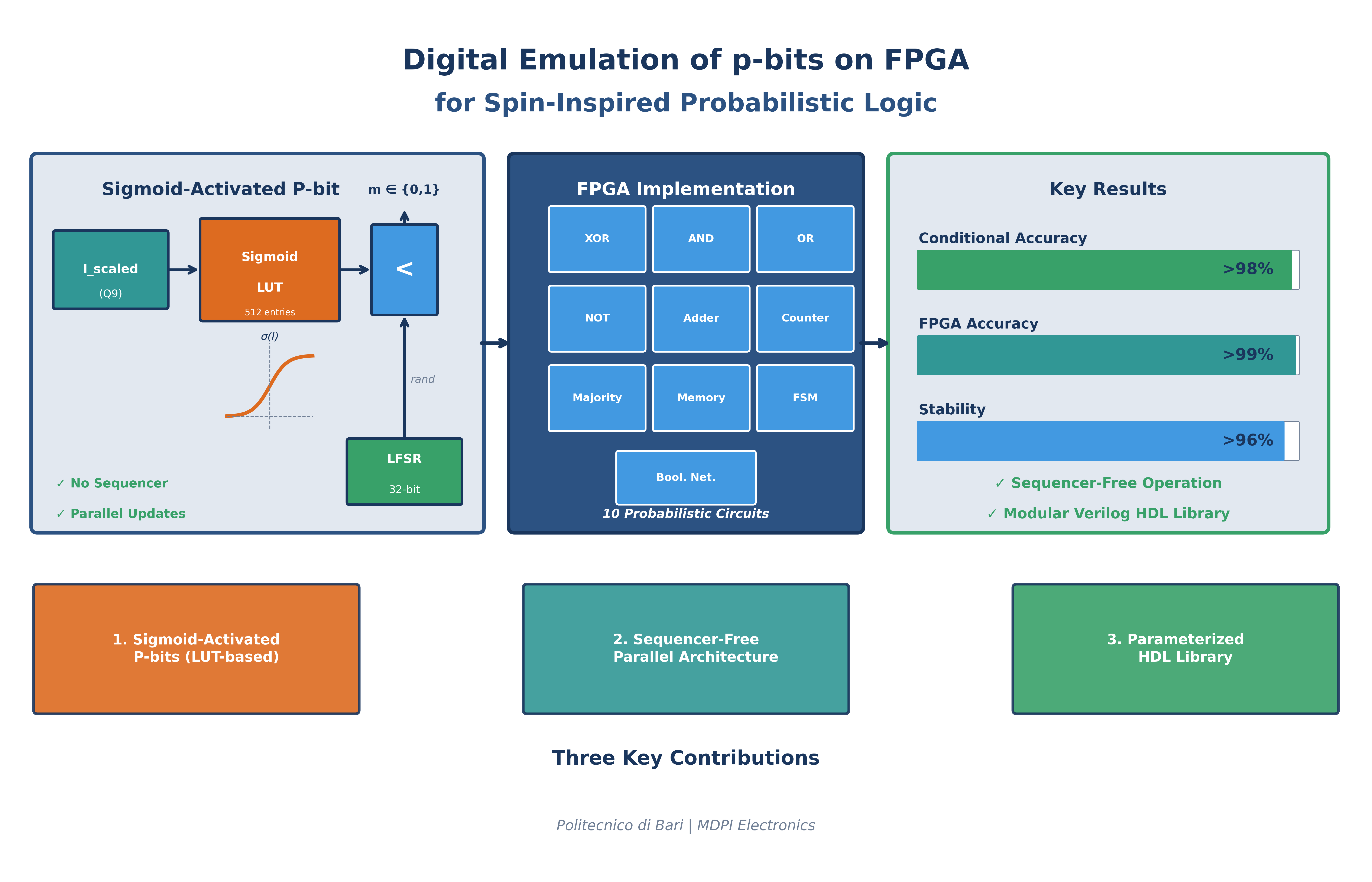
This paper presented a comprehensive FPGA-based framework for the digital emulation of spin-inspired probabilistic logic using sigmoid-activated p-bits. The main contributions of this work can be summarized as follows:
1. Direct hardware realization of sigmoid-activated p-bits. A LUT-based implementation of the sigmoid activation function enables precise and efficient control of probabilistic behavior without relying on costly arithmetic operations.
2. Sequencer-free, fully parallel architecture. Stable and accurate operation was demonstrated across ten probabilistic circuits—including four elementary logic gates (XOR, AND, OR, NOT), a full adder, a counter, a majority circuit, a memory cell, a Boolean network, and an FSM— achieving Conditional Accuracy exceeding 98% (reaching 99%+ for most circuits) and stability above 96% without the need for sequential updates.
3. Modular and reusable hardware library. A small set of parameterized Verilog HDL blocks (p-bit, LFSR, performance monitor, and sigmoid LUT) was reused across all designs, confirming scalability and portability across FPGA platforms.
4. Physical interpretability and controllability. The adopted parameterization directly maps to concepts such as interaction strength, bias, and effective temperature, facilitating the translation from theoretical probabilistic models to practical hardware implementations.
5. Enhanced debuggability and validation. The modular design and integrated monitoring infrastructure enable systematic validation and debugging, which are essential for the development of stochastic systems. All designs are validated against MATLAB reference implementations, ensuring reproducibility.
Overall, the proposed FPGA-based emulator provides both a practical experimentation platform and a scalable foundation for future probabilistic hardware accelerators. By bridging the gap between abstract probabilistic computing models and concrete digital implementations, this work contributes to the advancement of spin-inspired computing, neuromorphic systems, and stochastic hardware architectures. Future extensions will focus on hybrid update schemes, improved randomness sources, and larger probabilistic networks targeting optimization, inference, and learning applications.
By prioritizing architectural clarity, modular design, and reproducible behavior on reconfigurable hardware, this work complements existing device-oriented p-bit research and provides a concrete pathway toward deployable probabilistic accelerators on FPGA platforms.
Funding
This research received no external funding
Conflicts of Interest
The authors declare no conflicts of interest.
References
- Datta, S.; et al. Non-volatile spin switch for Boolean and non-Boolean logic. Appl. Phys. Lett. 2012, 101, 252411. [Google Scholar] [CrossRef]
- Camsari, K.Y.; et al. Implementing p-bits with embedded MTJ. IEEE Electron Device Lett. 2017, 38, 1767–1770. [Google Scholar] [CrossRef]
- Sutton, B.; et al. Intrinsic optimization using stochastic nanomagnets. Sci. Rep. 2017, 7, 1–9. [Google Scholar] [CrossRef] [PubMed]
- Datta, S. Quantum Transport: Atom to Transistor; Cambridge University Press: Cambridge, UK, 2005. [Google Scholar]
- Camsari, K.Y.; et al. Stochastic p-bits for invertible logic. Phys. Rev. X 2017, 7, 031014. [Google Scholar] [CrossRef]
- Hinton, G.E.; Sejnowski, T.J. Learning and relearning in Boltzmann machines. In Parallel Distributed Processing: Explorations in the Microstructure of Cognition; MIT Press: Cambridge, MA, USA, 1986; Volume 1, pp. 282–317. [Google Scholar]
- Ackley, D.H.; et al. A learning algorithm for Boltzmann machines. Cogn. Sci. 1985, 9, 147–169. [Google Scholar] [CrossRef]
- Weste, N.H.; Harris, D.M. CMOS VLSI Design: A Circuits and Systems Perspective; Addison-Wesley: Boston, MA, USA, 2010. [Google Scholar]
- Mizrahi, A.; et al. Neural-like computing with populations of superparamagnetic basis functions. Nat. Commun. 2018, 9, 1533. [Google Scholar] [CrossRef]
- Sengupta, S.; et al. Magnetic tunnel junction mimics stochastic cortical spiking neurons. Sci. Rep. 2016, 6, 30039. [Google Scholar] [CrossRef]
- Johnson, M.W.; et al. Quantum annealing with manufactured spins. Nature 2011, 473, 194–198. [Google Scholar] [CrossRef]
- Albash, T.; Lidar, D.A. Adiabatic quantum computation. Rev. Mod. Phys. 2018, 90, 015002. [Google Scholar] [CrossRef]
- Raychowdhury, A.; et al. Computing with networks of oscillatory dynamical systems. Proc. IEEE 2019, 107, 73–89. [Google Scholar] [CrossRef]
- Ielmini, D.; Wong, HS.P. In-memory computing with resistive switching devices. Nat Electron 2018, 1, 333–343. [Google Scholar] [CrossRef]
- Lucas, A. Ising formulations of many NP problems. Front. Phys. 2014, 2, 5. [Google Scholar] [CrossRef]
- Barahona, F.; et al. An application of combinatorial optimization to statistical physics and circuit layout design. Oper. Res. 1988, 36, 493–513. [Google Scholar] [CrossRef]
- Smolensky, P. Information processing in dynamical systems: Foundations of harmony theory. In Parallel Distributed Processing: Explorations in the Microstructure of Cognition; MIT Press: Cambridge, MA, USA, 1986; Volume 1, pp. 194–281. [Google Scholar]
- Hinton, G.E.; Salakhutdinov, R.R. Reducing the dimensionality of data with neural networks. Science 2006, 313, 504–507. [Google Scholar] [CrossRef]
- Robert, C.P.; Casella, G. Monte Carlo Statistical Methods; Springer: New York, NY, USA, 2013. [Google Scholar] [CrossRef]
- Gelman, A.; et al. Bayesian Data Analysis; CRC Press: Boca Raton, FL, USA, 2013. [Google Scholar] [CrossRef]
- Maass, W. Networks of spiking neurons: The third generation of neural network models. Neural Netw. 1997, 10, 1659–1671. [Google Scholar] [CrossRef]
- Camsari, K.Y.; Chowdhury, S.; Datta, S. Scalable emulation of sign-problem-free Hamiltonians with room-temperature p-bits. Phys. Rev. Appl. 2019, 12, 034061. [Google Scholar] [CrossRef]
- Pervaiz, A.Z.; Sutton, B.M.; Ghantasala, L.A.; Camsari, K.Y. Weighted p-bits for FPGA implementation of probabilistic circuits. IEEE Trans. Neural Netw. Learn. Syst. 2019, 30, 1920–1926. [Google Scholar] [CrossRef]
- Ercegovac, M.; Lang, T. Digital Arithmetic; Morgan Kaufmann: San Francisco, CA, USA, 2003. [Google Scholar]
- Coussy, P.; Morawiec, A. High-Level Synthesis: From Algorithm to Digital Circuit; Springer: Dordrecht, The Netherlands, 2008. [Google Scholar] [CrossRef]
- Hauck, S.; DeHon, A. Reconfigurable Computing: The Theory and Practice of FPGA-Based Computation; Morgan Kaufmann: Burlington, MA, USA, 2007. [Google Scholar]
- Compton, K.; Hauck, S. Reconfigurable computing: A survey of systems and software. ACM Comput. Surv. 2002, 34, 171–210. [Google Scholar] [CrossRef]
- Patterson, D.A.; Hennessy, J.L. Computer Architecture: A Quantitative Approach, 6th ed.; Morgan Kaufmann: Cambridge, MA, USA, 2017. [Google Scholar]
- Tessier, R.; Pocek, K.; DeHon, A. Reconfigurable computing architectures. Proc. IEEE 2015, 103, 332–354. [Google Scholar] [CrossRef]
- Betz, V.; Rose, J.; Marquardt, A. Architecture and CAD for Deep-Submicron FPGAs; Springer: Boston, MA, USA, 1999. [Google Scholar]
- Cong, J.; Ding, Y. FlowMap: An optimal technology mapping algorithm for delay optimization in lookup-table based FPGA designs. IEEE Trans. Comput.-Aided Des. Integr. Circuits Syst. 1994, 13, 1–12. [Google Scholar] [CrossRef]
- Ganssle, J. The Art of Designing Embedded Systems, 2nd ed.; Newnes: Burlington, MA, USA, 2008. [Google Scholar]
- Owens, J.D.; et al. GPU computing. Proc. IEEE 2008, 96, 879–899. [Google Scholar] [CrossRef]
- Kirk, D.B.; Hwu, W.-M.W. Programming Massively Parallel Processors: A Hands-on Approach, 3rd ed.; Morgan Kaufmann: Cambridge, MA, USA, 2016. [Google Scholar]
- Babu, P., Parthasarathy, E. Reconfigurable FPGA Architectures: A Survey and Applications. J. Inst. Eng. India Ser. B 102, 143–156 (2021). [CrossRef]
- Boutros, A.; Betz, V. FPGA architecture: Principles and progression. IEEE Circuits Syst. Mag. 2021, 21, 4–29. [Google Scholar] [CrossRef]
- Zhang, C.; et al. Optimizing FPGA-based accelerator design for deep convolutional neural networks. In Proceedings of the ACM/SIGDA International Symposium on Field-Programmable Gate Arrays, Monterey, CA, USA, 2015; pp. 161–170. [Google Scholar] [CrossRef]
- Umuroglu, Y.; et al. FINN: A framework for fast, scalable binarized neural network inference. In Proceedings of the ACM/SIGDA International Symposium on Field-Programmable Gate Arrays, Monterey, CA, USA, 2017; pp. 65–74. [Google Scholar] [CrossRef]
- Putnam, A.; et al. A reconfigurable fabric for accelerating large-scale datacenter services. ACM SIGARCH Comput. Archit. News 2014, 42, 13–24. [Google Scholar] [CrossRef]
- Firestone, D.; et al. Azure accelerated networking: SmartNICs in the public cloud. In Proceedings of the USENIX Symposium on Networked Systems Design and Implementation, Renton, WA, USA, 2018; pp. 51–66. [Google Scholar]
- Xilinx Inc. Versal ACAP: The First Adaptive Compute Acceleration Platform; White Paper WP505; Xilinx Inc.: San Jose, CA, USA, 2018.
- Brown, S.; Rose, J. FPGA and CPLD architectures: A tutorial. IEEE Des. Test Comput. 1996, 13, 42–57. [Google Scholar] [CrossRef]
- Krupnova, H.; Saucier, G. FPGA-Based Emulation: Industrial and Custom Prototyping Solutions; Springer: Boston, MA, USA, 2002. [Google Scholar]
- Alfke, P. Efficient Shift Registers, LFSR Counters, and Long Pseudo-Random Sequence Generators; Xilinx Application Note XAPP052; Xilinx Inc.: San Jose, CA, USA, 1996. [Google Scholar]
- B. Sunar, W. J. Martin and D. R. Stinson, “A Provably Secure True Random Number Generator with Built-In Tolerance to Active Attacks,” in IEEE Transactions on Computers, vol. 56, no. 1, pp. 109-119, Jan. 2007. [CrossRef]
- Majzoobi, M.; Koushanfar, F.; Devadas, S. FPGA-based true random number generation using circuit metastability with adaptive feedback control. In Proceedings of the International Workshop on Cryptographic Hardware and Embedded Systems (CHES), Nara, Japan, 2011; pp. 17–32. [Google Scholar] [CrossRef]
- Thomas, D.E.; Moorby, P.R. The Verilog® Hardware Description Language, 5th ed.; Springer: New York, NY, USA, 2008. [Google Scholar]
- Caulfield, A. M., Chung, E. S., Putnam, A., Angepat, H., Fowers, J., Haselman, M., Heil, S. F., Humphrey, M., Kaur, P., Kim, J.-Y., Daniel, L., Massengill, T., Ovtcharov, K., Papamichael, M. K., Woods, L., Lanka, S., Chiou, D., & Burger, D. (2016). A cloud-scale acceleration architecture. International Symposium on Microarchitecture, 1–13. 2016.
- Fowers, J. A Configurable Cloud-Scale DNN Processor for Real-Time AI. 2018 ACM/IEEE 45th Annual International Symposium on Computer Architecture (ISCA), Los Angeles, CA, USA, 2018; pp. 1–14. [Google Scholar] [CrossRef]
- Cai, B.; He, Y.; Xin, Y.; et al. Unconventional computing based on magnetic tunnel junction. Appl. Phys. A 2023, 129, 236. [Google Scholar] [CrossRef]
- Camsari, K.Y.; Sutton, B.M.; Datta, S. p-bits for probabilistic spin logic. Appl. Phys. Rev. 2019, 6, 011305. [Google Scholar] [CrossRef]
- Daniel, J.; Sun, Z.; Zhang, X.; Tan, Y.; Dilley, N.; Chen, Z.; Appenzeller, J. Experimental demonstration of an on-chip p-bit core based on stochastic magnetic tunnel junctions and 2D MoS₂ transistors. Nat. Commun. 2024, 15, 4067. [Google Scholar] [CrossRef] [PubMed]
- Smithson, S. C.; Onizawa, N.; Meyer, B. H.; Gross, W. J.; Hanyu, T. Efficient CMOS invertible logic using stochastic computing. IEEE Transactions on Circuits and Systems I: Regular Papers 2019, 66(6), 2263–2274. Article 8610326. [Google Scholar] [CrossRef]
- Liu, Y.; Hu, Q.; Wu, Q.; Liu, X.; Zhao, Y.; Zhang, D.; Han, Z.; Cheng, J.; Ding, Q.; Han, Y.; et al. Probabilistic Circuit Implementation Based on P-Bits Using the Intrinsic Random Property of RRAM and P-Bit Multiplexing Strategy. Micromachines 2022, 13, 924. [Google Scholar] [CrossRef]
- Victor H. González, Artem Litvinenko, Akash Kumar, Roman Khymyn, Johan Åkerman, Spintronic devices as next-generation computation accelerators, Current Opinion in Solid State and Materials Science, Volume 31, 2024, 101173, ISSN 1359-0286.
- Li, Z.; Zhang, Y.; Sui, B.; Xing, Z.; Wang, Q. FPGA implementation for the sigmoid with piecewise linear fitting based on curvature analysis. Electronics 2022, 11, 1365. [Google Scholar] [CrossRef]
- Venkatesh, S.; Sindhu, R.R.; Arunachalam, V.V. Hardware Efficient Approximate Sigmoid Activation Function for Classifying Features Around Zero. Integration 2025, 103, 102421. [Google Scholar] [CrossRef]
- Serhiienko, P., Sergiyenko, A., Telenyk, S., Nowakowski, G. (2024). Calculation of the Sigmoid Activation Function in FPGA Using Rational Fractions. In: Franco, L., de Mulatier, C., Paszynski, M., Krzhizhanovskaya, V.V., Dongarra, J.J., Sloot, P.M.A. (eds) Computational Science – ICCS 2024. ICCS 2024. Lecture Notes in Computer Science, vol 14837. Springer, Cham. [CrossRef]
- Matuszewski, Ł.; Jessa, M. A Low-Complexity Start–Stop True Random Number Generator for FPGAs. Appl. Sci. 2024, 14, 5642. [Google Scholar] [CrossRef]
- Matsubara, S. et al. (2018). Ising-Model Optimizer with Parallel-Trial Bit-Sieve Engine. In: Barolli, L., Terzo, O. (eds) Complex, Intelligent, and Software Intensive Systems. CISIS 2017. Advances in Intelligent Systems and Computing, vol 611. Springer, Cham. [CrossRef]
- G. G. Ko, Y. Chai, R. A. Rutenbar, D. Brooks and G. -Y. Wei, “FlexGibbs: Reconfigurable Parallel Gibbs Sampling Accelerator for Structured Graphs,” 2019 IEEE 27th Annual International Symposium on Field-Programmable Custom Computing Machines (FCCM), San Diego, CA, USA, 2019, pp. 334-334. [CrossRef]
- L. Li, H. Wang, Z. Xie, Z. Liu, W. Cui and Y. Pan, “Simulated Ising Annealing Algorithm with Gaussian Augmented Hamiltonian Monte Carlo,” 2023 42nd Chinese Control Conference (CCC), Tianjin, China, 2023, pp. 6760-6765,. [CrossRef]
- Borders, W.A.; et al. Integer factorization using stochastic magnetic tunnel junctions. Nature 2019, 573, 390–393. [Google Scholar] [CrossRef] [PubMed]
- Camsari, K.Y.; et al. Scaled quantum circuits emulated with room temperature p-bits. arXiv 2019. [Google Scholar] [CrossRef]
Figure 1.
Block diagram of the proposed sigmoid-activated p-bit. The signed interaction input is scaled using configurable parameters and BIAS, clipped to the interval (Q9 format corresponding to [−2.0, +2.0]), processed by a 512-entry sigmoid lookup table (LUT), and compared with a 32-bit LFSR-generated pseudo-random number to produce a stochastic binary output implementing Bernoulli sampling.
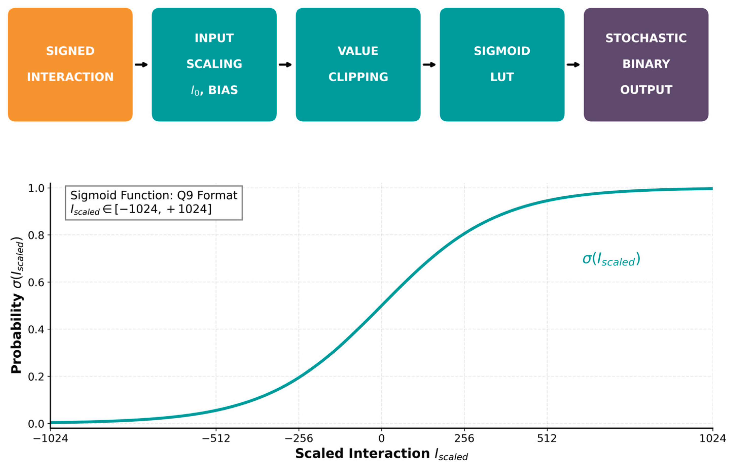
Figure 2.
Algorithmic representation of the sigmoid-based p-bit cell. The interaction input (Q9 fixed-point) is mapped to a probability through a 512-entry sigmoid LUT (with Q9-to-real normalization by 512) and compared with a 32-bit LFSR-generated pseudo-random number. The output is a Bernoulli stochastic variable with activation probability .
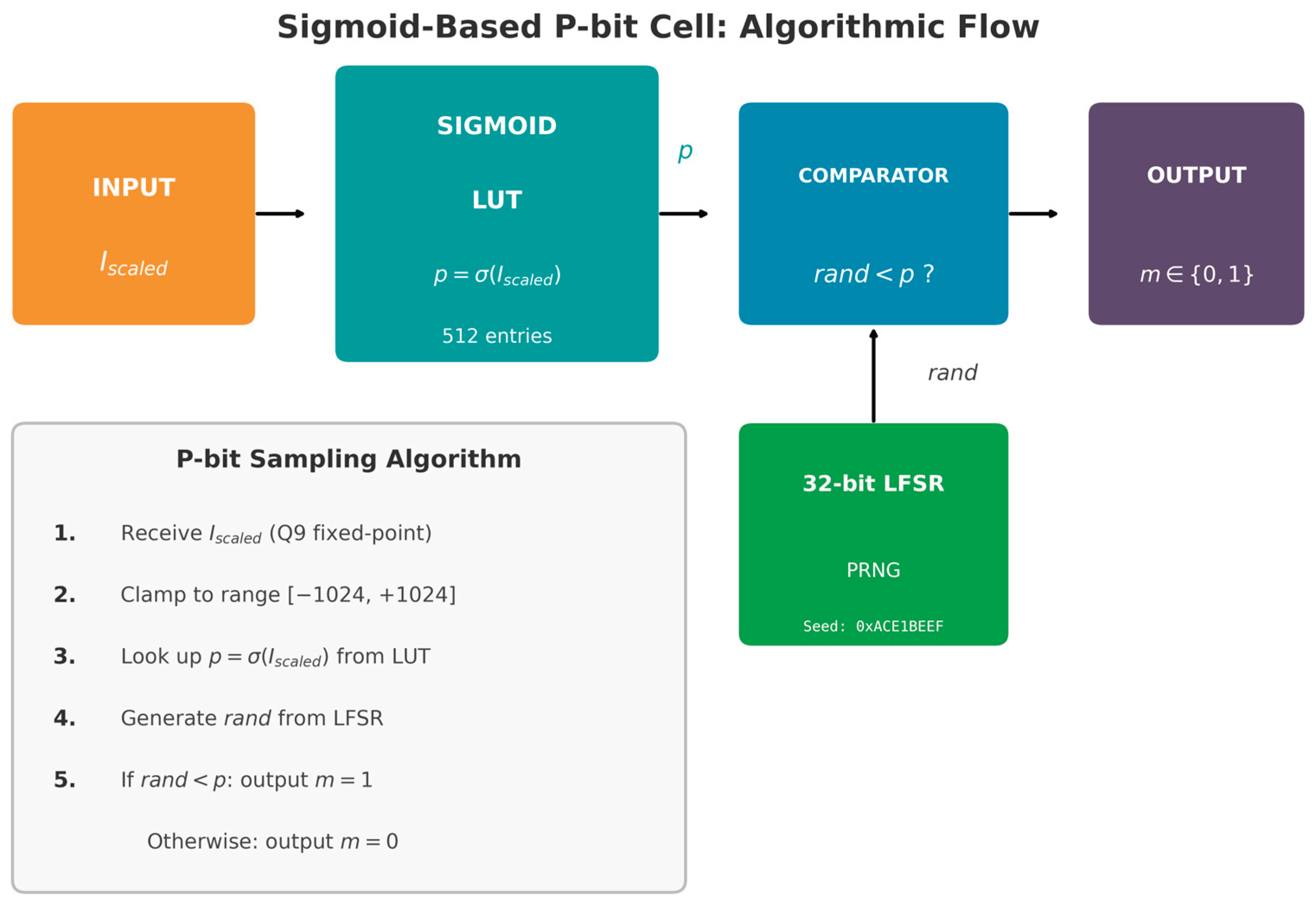
Figure 3.
Architecture of the probabilistic XOR gate implemented using the proposed p-bit modules. Boolean inputs m₀ and m₁ are mapped to bipolar spin variables s₀, s₁ ∈ {±512} (Q9 format, corresponding to ±1.0). The interaction term I = BIAS − 3(s₀ × s₁), with BIAS = −1024, is computed in fixed-point arithmetic and fed to a sigmoid-activated p-bit together with a 32-bit LFSR-generated pseudo-random number (seed: 0xACE1BEEF), yielding a sequencer-free probabilistic XOR output.
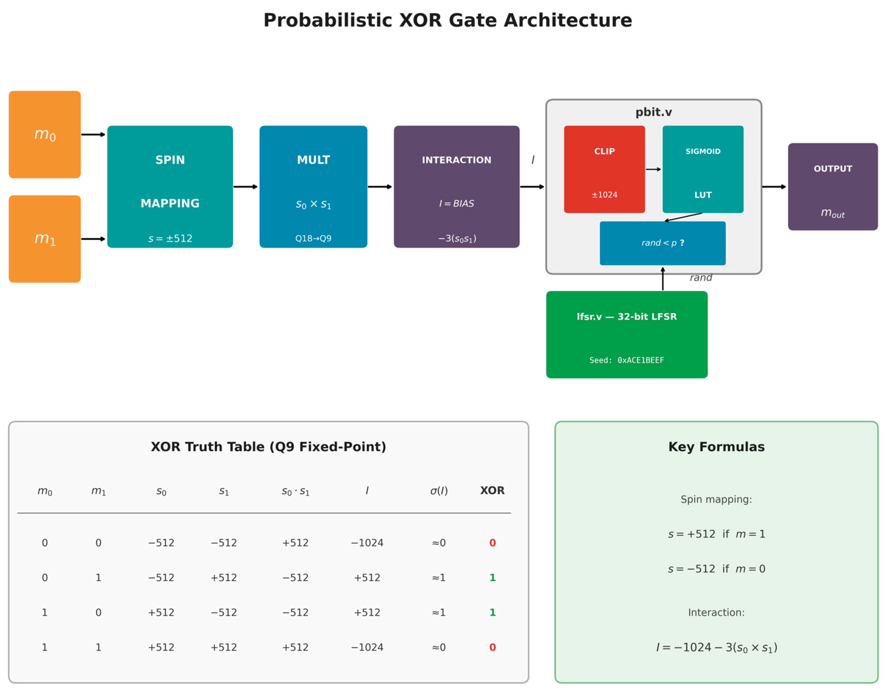

Table 1.
Summary of the main architectural differences across FPGA, GPU, and microcontroller platforms.
Table 1.
Summary of the main architectural differences across FPGA, GPU, and microcontroller platforms.
| Feature | FPGA | GPU | Microcontroller |
|---|---|---|---|
| Granularity | Bit-level, fully customizable | Block-level, limited control | Instruction-level |
| Parallelism | High, customizable | High, but general-purpose | Low |
| Latency | Low, deterministic | Moderate–high, non-deterministic | Application-dependent |
| Energy Efficiency | High | Moderate–low | High, but limited scalability |
| Scalability | High | Moderate | Low |
| Flexibility | Very high (reconfigurable) | Moderate (software-defined) | Low |
Table 2.
Summary of key design trade-offs in FPGA-based p-bit emulation.
| Aspect | Design Options | Advantages | Limitations / Trade-offs |
|---|---|---|---|
| Activation Function | LUT-based sigmoid; piecewise linear; rational/Taylor approximations | LUT: simplest and fully parallel; PWLC: best resource efficiency; Rational: high precision | LUT may require large BRAM; PWLC needs segmentation tuning; Rational increases DSP usage |
| Randomness Source | LFSR (PRNG); TRNG (ring-oscillator/metastable) | PRNG: reproducible, easily synchronized; TRNG: higher entropy, physics-like noise | PRNGs less “physical”; TRNGs need careful calibration and consume analog resources |
| Update Scheduling | Sequential; block-parallel; fully parallel | Sequential: exact Boltzmann statistics; Parallel: highest throughput, no control FSM | Parallel updates may introduce minor correlation unless inputs are decorrelated |
| Scalability | Parameterized p-bit modules and reusable IP cores | Modular synthesis, flexible array sizing | Resource overhead grows quadratically with network density |
| Performance Metrics | Throughput, energy per update, mean-matching error (MME), correlation accuracy (CA) | Clear comparison of architectures | Accuracy vs. resource trade-off must be characterized empirically |
Table 3.
Truth table and interaction values for the probabilistic XOR gate. Boolean inputs m₀ and m₁ are mapped to bipolar spin variables s₀ and s₁ (Q9 fixed-point format). The interaction term I is computed as I = BIAS − 3 × (s₀ × s₁) and clipped to the range [−1024, +1024]. The column σ(I) reports the effective activation probability obtained from the sigmoid lookup table, which incorporates an implicit gain resulting in a steep, near-deterministic response consistent with the implemented FPGA architecture.
| m₀ | m₁ | s₀ | s₁ | s₀×s₁ (Q9) | I (before clipping) | I (after clipping) | Expected XOR |
|---|---|---|---|---|---|---|---|
| 0 | 0 | −512 | −512 | +512 | −2560 | −1024 | 0 |
| 0 | 1 | −512 | +512 | −512 | +512 | +512 | 1 |
| 1 | 0 | +512 | −512 | −512 | +512 | +512 | 1 |
| 1 | 1 | +512 | +512 | +512 | −2560 | −1024 | 0 |
Table 4.
Common parameters shared across all probabilistic circuit implementations.
| Module | Parameter | Value | Description |
|---|---|---|---|
| pbit.v | DATA_WIDTH | 16 | Fixed-point word length (Q9 format) |
| RAND_WIDTH | 32 | Bit width of random number input | |
| LUT_SIZE | 512 | Number of entries in sigmoid LUT | |
| SIGMOID_WIDTH | 16 | Bit width of LUT probability output | |
| lfsr.v | WIDTH | 32 | Bit width of pseudo-random generator |
| SEED | 32’hACE1BEEF | Initialization seed for LFSR state | |
| Evaluation | N | 100000 | Number of samples per input condition |
Table 5.
Application-specific parameters for the XOR probabilistic gate.
| Module | Parameter | Value | Description |
|---|---|---|---|
| pbit_xor.v | I₀ | 1024 | Scaling factor (2.0 in Q9) |
| BIAS | −1024 | Bias term (−2.0 in Q9) | |
| pbit.v | I₀ | 1024 | Scaling factor for sigmoid input |
| BIAS | 0 | Internal bias (external bias used) |
Table 6.
Comparative results for the XOR probabilistic gate. Matlab simulations are used as reference values, while ModelSim emulation on FPGA validates the hardware implementation.
Table 6.
Comparative results for the XOR probabilistic gate. Matlab simulations are used as reference values, while ModelSim emulation on FPGA validates the hardware implementation.
| Input | Expected | MATLAB Mean | MATLAB CA (%) | MATLAB CE (%) | ModelSim Mean | ModelSim CA (%) | ModelSim CE (%) | Stability (%) |
|---|---|---|---|---|---|---|---|---|
| 00 | 0 | 0.000 | 100.00 | 0.00 | 0.001 | 99.95 | 0.05 | 99.96 |
| 01 | 1 | 0.981 | 98.11 | 1.89 | 1.000 | 99.96 | 0.04 | 99.96 |
| 10 | 1 | 0.981 | 98.07 | 1.93 | 1.000 | 99.97 | 0.03 | 99.96 |
| 11 | 0 | 0.000 | 100.00 | 0.00 | 0.000 | 99.98 | 0.02 | 99.97 |
Table 7.
Application-specific parameters for the AND probabilistic gate.
| Module | Parameter | Value | Description |
|---|---|---|---|
| pbit_and.v | I₀ | 1024 | Scaling factor (2.0 in Q9) |
| BIAS | 0 | No additional bias | |
| Interaction | s₀ + s₁ − 512 | AND logic encoding |
Table 8.
Comparative results for the AND probabilistic gate.
| Input | Expected | MATLAB Mean | MATLAB CA (%) | MATLAB CE (%) | ModelSim Mean | ModelSim CA (%) | ModelSim CE (%) | Stability (%) |
|---|---|---|---|---|---|---|---|---|
| 00 | 0 | 0.000 | 100.00 | 0.00 | 0.000 | 99.96 | 0.04 | 99.97 |
| 01 | 0 | 0.018 | 98.24 | 1.76 | 0.000 | 99.97 | 0.03 | 99.96 |
| 10 | 0 | 0.019 | 98.08 | 1.92 | 0.000 | 99.96 | 0.04 | 99.97 |
| 11 | 1 | 0.981 | 98.13 | 1.87 | 1.000 | 99.97 | 0.03 | 99.96 |
Table 9.
Application-specific parameters for the OR probabilistic gate.
| Module | Parameter | Value | Description |
|---|---|---|---|
| pbit_or.v | I₀ | 1024 | Scaling factor (2.0 in Q9) |
| BIAS | +512 | Positive bias (+1.0 in Q9) |
Table 10.
Comparative results of the OR probabilistic gate.
| Input | Expected | MATLAB Mean | MATLAB CA (%) | MATLAB CE (%) | ModelSim Mean | ModelSim CA (%) | ModelSim CE (%) | Stability (%) |
|---|---|---|---|---|---|---|---|---|
| 00 | 0 | 0.017 | 98.26 | 1.74 | 0.000 | 99.96 | 0.04 | 99.97 |
| 01 | 1 | 0.980 | 97.98 | 2.02 | 1.000 | 99.97 | 0.03 | 99.96 |
| 10 | 1 | 0.984 | 98.38 | 1.62 | 1.000 | 99.96 | 0.04 | 99.96 |
| 11 | 1 | 1.000 | 100.00 | 0.00 | 1.000 | 99.97 | 0.03 | 99.97 |
Table 11.
Application-specific parameters for the NOT probabilistic gate.
| Module | Parameter | Value | Description |
|---|---|---|---|
| pbit_not.v | I₀ | 1024 | Scaling factor (2.0 in Q9) |
| BIAS | 0 | No additional bias | |
| Interaction | −s₀ | Input negation |
Table 12.
Comparative results for the NOT probabilistic gate.
| Input | Expected | MATLAB Mean | MATLAB CA (%) | MATLAB CE (%) | ModelSim Mean | ModelSim CA (%) | ModelSim CE (%) | Stability (%) |
|---|---|---|---|---|---|---|---|---|
| 0 | 1 | 0.984 | 98.36 | 1.64 | 1.000 | 99.96 | 0.04 | 96.00 |
| 1 | 0 | 0.019 | 98.13 | 1.87 | 0.000 | 99.97 | 0.03 | 96.00 |
Table 13.
Application-specific parameters for the Boolean network.
| Module | Parameter | Value | Description |
|---|---|---|---|
| pbit_boolean_network.v | I₀ | 1024 | Scaling factor (2.0 in Q9) |
| BIAS | 0 | No additional bias |
Table 14.
Comparative results for the Boolean network.
| Input | Expected | MATLAB Mean | MATLAB CA (%) | ModelSim Mean | ModelSim CA (%) | Stability (%) |
|---|---|---|---|---|---|---|
| 000 | 0 | 0.000 | 100.0 | 0.000 | 99.96 | 98.71 |
| 001 | 1 | 0.984 | 98.4 | 0.999 | 99.95 | 98.71 |
| 010 | 0 | 0.000 | 100.0 | 0.000 | 99.98 | 98.71 |
| 011 | 1 | 0.984 | 98.2 | 0.999 | 99.94 | 98.71 |
| 100 | 0 | 0.000 | 100.0 | 0.000 | 99.99 | 98.71 |
| 101 | 1 | 0.982 | 98.1 | 1.000 | 99.96 | 98.71 |
| 110 | 1 | 0.985 | 98.2 | 1.000 | 99.97 | 98.71 |
| 111 | 1 | 0.988 | 98.8 | 1.000 | 99.97 | 98.71 |
Table 15.
Application-specific parameters of the probabilistic full adder.
| Parameter | Value | Description |
|---|---|---|
| BIAS_SUM | −1024 (−2.0 in Q9) | Bias for 3-input XOR (sum output) |
| BIAS_COUT | 0 | Bias for majority function (carry output) |
| Spin values | ±512 (±1.0 in Q9) | Bipolar encoding of inputs |
Table 16.
Comparative results.
| Input (A,B,Cin) | Expected (S,Cout) | MATLAB Sum CA (%) | MATLAB Cout CA (%) | ModelSim Sum CA (%) | ModelSim Cout CA (%) | Stability (%) |
|---|---|---|---|---|---|---|
| 000 | (0, 0) | 100.00 | 100.00 | 99.9 | 100.0 | 99.5 |
| 001 | (1, 0) | 98.23 | 98.16 | 99.9 | 99.9 | 99.5 |
| 010 | (1, 0) | 98.22 | 98.23 | 100.0 | 100.0 | 99.5 |
| 011 | (0, 1) | 100.00 | 98.26 | 99.9 | 100.0 | 99.5 |
| 100 | (1, 0) | 98.26 | 98.28 | 99.9 | 100.0 | 99.5 |
| 101 | (0, 1) | 100.00 | 98.21 | 100.0 | 100.0 | 99.5 |
| 110 | (0, 1) | 100.00 | 98.22 | 99.9 | 100.0 | 99.5 |
| 111 | (1, 1) | 98.19 | 100.00 | 100.0 | 100.0 | 99.5 |
Table 17.
Application-specific parameters of the probabilistic counter.
| Parameter | Value | Description |
|---|---|---|
| I₀ | 1024 (2.0 in Q9) | Scaling factor |
| J | 768 (1.5 in Q9) | Coupling parameter |
| BIAS | 0 | No additional bias |
| N | 100,000 | Observation window |
Table 18.
Comparative results for the probabilistic counter.
| Metric | MATLAB | ModelSim | Expected |
|---|---|---|---|
| Final Count | 99.81 | 99.00 | ~99.00 |
| Probability (%) | 99.81 | 99.00 | ~99 |
| CA (%) | 99.81 | 99.95 | >98 |
| CE (%) | 0.19 | 0.05 | <2 |
| Stability (%) | 99.8 | 99.9 | >96 |
Table 19.
Application-specific parameters of the probabilistic majority gate.
| Module | Parameter | Value | Description |
|---|---|---|---|
| pbit_majority.v | POS_INTERACTION | +768 (+1.5 in Q9) | Interaction when majority = 1 |
| NEG_INTERACTION | −768 (−1.5 in Q9) | Interaction when majority = 0 | |
| NOISE_FACTOR | 128 (0.25 in Q9) | Amplitude of injected noise | |
| perf_monitor | WINDOW_SIZE | 100000 | Samples for evaluation |
Table 20.
Comparative results for the probabilistic majority circuit including temporal and statistical metrics.
Table 20.
Comparative results for the probabilistic majority circuit including temporal and statistical metrics.
| Input | Tool | Mean | CA (%) | CE (%) | Stab. (%) |
|---|---|---|---|---|---|
| 000 | MATLAB | 0.000 | 99.67 | 0.33 | ~99 |
| ModelSim | 0.000 | 100.00 | 0.00 | ~99 | |
| 001 | MATLAB | 0.000 | 99.68 | 0.32 | ~99 |
| ModelSim | 0.000 | 99.96 | 0.04 | ~99 | |
| 010 | MATLAB | 0.000 | 99.69 | 0.31 | ~99 |
| ModelSim | 0.000 | 99.97 | 0.03 | ~99 | |
| 011 | MATLAB | 0.999 | 99.68 | 0.32 | ~99 |
| ModelSim | 1.000 | 99.96 | 0.04 | ~99 | |
| 100 | MATLAB | 0.000 | 99.64 | 0.36 | ~99 |
| ModelSim | 0.000 | 99.95 | 0.05 | ~99 | |
| 101 | MATLAB | 0.999 | 99.66 | 0.34 | ~99 |
| ModelSim | 1.000 | 99.96 | 0.04 | ~99 | |
| 110 | MATLAB | 0.999 | 99.64 | 0.36 | ~99 |
| ModelSim | 1.000 | 99.96 | 0.04 | ~99 | |
| 111 | MATLAB | 0.999 | 99.70 | 0.30 | ~99 |
| ModelSim | 1.000 | 99.95 | 0.05 | ~99 |
Table 21.
Application-specific parameters of the probabilistic memory cell.
| Parameter | Value | Description |
|---|---|---|
| I₀ | 512 (1.0 in Q9) | Scaling factor |
| BIAS | −1024 (−2.0 in Q9) | Bias for bistability |
| FEEDBACK_COEFF | 3 | Positive feedback strength |
| CLIP_VAL | 2048 (±4.0 in Q9) | Clipping threshold |
Table 22.
Comparative results for the probabilistic memory cell.
| Init State | Tool | Mean | CA (%) | CE (%) | Stability (%) |
|---|---|---|---|---|---|
| 0 | MATLAB | 0.000 | 100.00 | 0.00 | 100.00 |
| 0 | ModelSim | 0.000 | 99.96 | 0.04 | 99.96 |
| 1 | MATLAB | 1.000 | 100.00 | 0.00 | 100.00 |
| 1 | ModelSim | 1.000 | 99.96 | 0.04 | 99.96 |
Table 23.
Application-specific parameters of the probabilistic FSM.
| Parameter | Value | Description |
|---|---|---|
| Number of states | 4 | S₀, S₁, S₂, S₃ |
| State encoding | 2 bits | Binary state representation |
| Bias (S₀, S₃) | −4.0 (Q1.14) | Strong negative bias |
| Bias (S₁, S₂) | +4.0 (Q1.14) | Strong positive bias |
| MIN_TIME | 50 cycles | Minimum residence time |
| Transition prob. (S₀, S₃) | 0.1 | Exit probability |
| Transition prob. (S₁, S₂) | 0.05 | Exit probability (conditional) |
| Timeout | 2 × MIN_TIME | Deterministic exit guarantee |
Table 24a.
Per-state accuracy and output probability for the probabilistic FSM (ModelSim, N=100000 cycles).
Table 24a.
Per-state accuracy and output probability for the probabilistic FSM (ModelSim, N=100000 cycles).
| State | Encoding | Bias | Accuracy (%) | P(out=1) (%) |
|---|---|---|---|---|
| S0 | 00 | −4.0 | 99.98 | 0.02 (expected ≈0) |
| S1 | 01 | +4.0 | 97.40 | 97.40 (expected ≈100) |
| S2 | 10 | +4.0 | 99.97 | 99.97 (expected ≈100) |
| S3 | 11 | −4.0 | 96.93 | 3.07 (expected ≈100) |
Table 24b.
Global metrics for the probabilistic FSM.
| Metric | MATLAB (N=100000) | ModelSim (N=100000) |
|---|---|---|
| Global Accuracy (%) | 99.54 | 98.57 |
| Classification Error (%) | 0.046 | 1.43 |
| Global Stability (%) | 99 | 99 |
Table 25.
Summary of results for all probabilistic circuits.
| Circuit | Inputs | Outputs | MATLAB CA (avg) | FPGA CA (avg) | FPGA Stability | Sequencer |
|---|---|---|---|---|---|---|
| XOR | 2 | 1 | 99.05% | 99.97% | >99% | No |
| AND | 2 | 1 | 98.61% | 99.97% | >99% | No |
| OR | 2 | 1 | 98.66% | 99.97% | >99% | No |
| NOT | 1 | 1 | 98.25% | 99.97% | 96% | No |
| Boolean Network | 3 | 1 | 98.96% | 99.97% | 98.71% | No |
| Full Adder | 3 | 2 | 98.89% | 99.96% | >99% | No |
| Counter | 1 | 1 | 99.81% | 99.95% | 99.9% | No |
| Majority | 3 | 1 | 99.67% | 99.97% | ~99% | No |
| Memory Cell | 1 | 1 | 100.00% | 99.96% | 99.96% | No |
| FSM | — | — | 99.54% | 98.57% | ~99% | No |
Table 26.
Comparison between LUT-sigmoid p-bit and weighted p-bit architectures.
| Feature | LUT-Sigmoid (This Work) | Weighted p-bit [23] |
|---|---|---|
| Update scheme | Fully parallel | Sequential (Gibbs) |
| Sequencer required | No | Yes |
| CA achieved | >98.57% | ~98% (reported) |
| Stability | >96% | Requires sequencer |
| Control logic complexity | Minimal | Higher (sequencer FSM) |
| Best suited for | Feed-forward, FSMs, logic | Boltzmann machines, invertible logic |
Disclaimer/Publisher’s Note: The statements, opinions and data contained in all publications are solely those of the individual author(s) and contributor(s) and not of MDPI and/or the editor(s). MDPI and/or the editor(s) disclaim responsibility for any injury to people or property resulting from any ideas, methods, instructions or products referred to in the content. |
© 2026 by the authors. Licensee MDPI, Basel, Switzerland. This article is an open access article distributed under the terms and conditions of the Creative Commons Attribution (CC BY) license (http://creativecommons.org/licenses/by/4.0/).
Copyright: This open access article is published under a Creative Commons CC BY 4.0 license, which permit the free download, distribution, and reuse, provided that the author and preprint are cited in any reuse.


