Submitted:
25 December 2025
Posted:
25 December 2025
You are already at the latest version
Abstract
With the shift of oil and gas exploitation to deep seas, the 35 kV high-voltage electric slip ring in Single-Point Mooring (SPM) systems faces critical challenges of insulation failure and thermal failure, threatening operational safety. This study aims to investigate its insulation strength and temperature rise characteristics. A three-dimensional electric field model and a magnetic-thermal coupling model considering the skin effect were established using the finite element method (FEM). Simulations were conducted under four high-voltage configurations and various high-current operating conditions, followed by AC breakdown tests and high-current temperature rise experiments for validation. Results show that the maximum electric field (up to 19.53 kV/mm) concentrates at the inlet PTFE bushing, which is the insulation weak point. The maximum temperature rise at the center ring can be predicted by a power-law model. Moreover, simulation results agree well with experimental data, confirming the reliability of the computational studies. This work provides a theoretical and experimental basis for the optimal design and safe operation of high-voltage slip rings in offshore SPM systems.
Keywords:
Single-Point Mooring
; electric slip ring
; electric field simulation
; heat transfer simulation
; 35 kV high voltage devices
1. Introduction
With the depletion of onshore and shallow-sea oil and gas resources, the development of deep-sea oil and gas has become important to meet the growing global energy demand. Submarine oil and gas resources account for 1/3 of the world’s total oil and gas reserves, and the number of deep-sea and ultra-deep-sea oilfields has exceeded six times that of shallow-sea oilfields, driving the gradual shift of oil and gas exploitation activities toward deep-sea areas and the formation of large-scale oilfield clusters [1]. As a core component of deep-sea oil and gas exploitation systems, the Floating Production Storage and Offloading (FPSO) relies on the Single-Point Mooring (SPM) system to achieve reliable power transmission and fluid transfer with subsea facilities. To address the requirements of longer transmission distances and larger processing capacities in deep-sea operations, the SPM system is developing toward high voltage and high power. For instance, 35 kV high-voltage SPM has been widely adopted due to its significant advantage in reducing power loss compared to the traditional 10 kV mode. However, the increase in voltage and power brings prominent challenges, including (1) insulation failure caused by uneven electric field distribution [2] and (2) thermal failure induced by high current load [3], potentially leading to platform shutdowns and huge economic losses. Therefore, investigating the insulation performance and temperature rise characteristics of 35 kV high-voltage slip rings is of great engineering significance for ensuring the safe operation of deep-sea oil and gas exploitation platforms.
Existing studies on the reliability of SPM systems primarily focus on insulation failures caused by defective contact between brushes and collector rings, as well as uneven current distribution in electrical slip rings. For instance, Wang et al. analyzed key parameters such as contact statics and main loop resistance of slip rings and verified the reliability of self-designed slip rings through dynamic and static continuous high-current engineering tests [4]. Feng et al. conducted tests on the contact current distribution of electrical slip rings at different angles and confirmed the uneven current transmission among various contacts [5]. Additionally, our team conducted preliminary simulation on the electric and thermal field inside a 35 kV slip ring prototype [6,7]. However, there remains a research gap in two critical aspects: first, studies on insulation failures induced by uneven electric field distribution in SPM systems are relatively scarce, and the precise location of high-electric-field regions have not been fully clarified. Second, research on the temperature distribution inside SPM slip rings and the effects of current load, heat dissipation and ambient environment is still insufficient.
To fill the aforementioned research gaps, this paper conducts a comprehensive computational and experimental analysis on the insulation strength and temperature rise of a 35 kV electric slip ring prototype for offshore SPM systems. The main work includes three key parts: First, a three-dimensional electric field simulation model of the slip ring is established based on the finite element method (FEM) using COMSOL software. Second, a coupled magnetic-thermal simulation model considering the skin effect is developed to analyze the temperature rise characteristics of the slip ring, which is also used to investigate the effects of current load, convective heat transfer coefficient, and ambient temperature on temperature rise. A power-law prediction model for temperature rise is also established via multivariable linear regression. Third, experimental validations, including AC breakdown test and temperature rising test, are performed to verify the reliability of the simulation results. The results show good agreement between simulation and experiment, providing a reliable basis for the optimal design and safe operation of 35 kV high-voltage slip rings in SPM systems.
2. Methods of Electric and Thermal Simulation
2.1. Structure of the 35kV Slip-Ring Prototype Device
Prototype device of the 35 kV electric slip ring is shown in Figure 1a. With a rated voltage of 35 kV and rated current of 640 A, the device has a polygonal prism structure featuring a circumcircle diameter of 1,930 mm and overall height of 2,400 mm. Utilizing the three-phase, four-wire AC power configuration, the prototype sequentially integrates four slip rings from top to bottom, i.e., A-phase, B-phase, C-phase, and neutral point. Copper busbars with a cross-sectional area of 80 × 15 mm are installed on both the lateral surfaces and central underside for power input and output.
As shown in Figure 1a, the insulation system employs four PTFE bushings to insulate the horizonal busbar and the outer shell. Moreover, several composite support insulators, consisting of epoxy resin core rods and silicone rubber sheaths, are utilized to isolate different voltages between adjacent slip rings as well as ring grounded electrodes. The inter-phase spacing between slip rings progressively increases from top to bottom as 180 mm, 240 mm, and 300 mm respectively, while the clearance between slip rings and the grounded enclosure measures 300 mm. As shown in Figure 1b, four C-shape connectors are used in each slip-rings as the sliding electrical contact between the fixed, outer frame and the rotatable, inner rings.
2.2. Calculation Model of Electric Field
2.2.1. Maxwell Equations of Quasi-static Electric Field
The electric field in a certain domain is determined by the Maxwell equations [8], which can be expressed as:
where D is the electric flux density in C/m2; B is the magnetic flux density in T; E is the electric field in V/m; H is the magnetic field in A/m; ρ is the electric charge density in C/m3; J is the electric current density in A.
The relationship between flux/current variables (D, B and J) and field variables (E and H) can be determined by the material equations (i.e., constitutive equations):
where ε0 = 8.854 × 10⁻¹² F/m is the vacuum permittivity of electric field and εr is the relative permittivity; μ0 = 4π × 10-7 H/m is the vacuum permeability of magnetic field and μr is the relative permeability of insulation materials; σ is the electric conductivity in S/m.
Since the insulation structure of the slip ring prototype (< 2 m) is much smaller than the wavelength of 50 Hz electromagnetic field (6000 km), the electro-quasi-static (EQS) assumption can be used in the electric field analysis, i.e., the electric curl field induced by the time derivative of magnetic field can be neglected. Therefore, the equations in (1) and (2) can be rearranged to the following equations:
Considering that the insulation performance of the slip ring prototype is mainly correlated to the electric field E, and the Helmholtz Theorem indicates that a vector is determined if the curl and divergence of this vector is specified under certain boundary conditions, equation (3) can be further simplified to determine the quasi-static E field as:
In equation (4), the 3rd line indicates that the curl of electric field is zero, this implies that the vector-form electric field E is conservative (i.e. irrotational). This means that the electric field is equivalent to the gradient of a scalar-form field. Herein, the electric potential V is used as this scalar field, and V and E has the following relationship
Taking consideration of the 1st and 2nd equations in (4) and equation (5), the electric potential V in the insulation system of slip ring prototype can be determined by
2.2.2. Simplification of V-Field Equation Under AC 50Hz Voltage
Since the slip ring is operated at 50Hz power frequency, equation (6) can be transferred into the frequency domain using the Fourier transform, which can be expressed as
where is the phasor of the electric potential, ω = 100π rad/s is the angular frequency of the 50Hz sinusoidal voltage waveform. Equation (7) is the Laplace equation of frequency-domain electric potential, considering both the permittivity and conductivity of the dielectric materials.
Although it appears to be complex, this expression can be further simplified based on the properties of insulation materials. As shown in Table 1, the permittivity term (ωε0εr) is 3 to 5 orders of magnitude higher than the conductivity term in the dielectric materials of 50Hz slip ring prototype. Thus, the contribution of electrical conductivity on the potential distribution can be neglected. And equation (7) can be transformed to
Considering that ω and ε0 are constant, and the relative permittivity in the problem domain can be varied due to the spatial transition of different insulation materials. Equation (8) can be further simplified to
Obviously, equation (9) has the similar form to the Laplace equation of electrostatic field, indicating that the electric field distribution under AC 50Hz voltage excitation can be calculated using the electrostatic model.
2.2.3. Boundary Conditions of Electric Field
During the simulation of electric field, there are mainly two types of boundary conditions, i.e., the potential boundary at the conductor’s surface and the continuity conditions at the dielectric interface. Details of these boundary conditions are described below
- 1)
- Potential boundary at the conductor’s surface
The potential boundary condition, also known as the Dirichlet boundary condition, is one of the most widely used boundary conditions in electric field simulation. It is defined by specifying the exact electric potential value (V) at every point on a given boundary, including the high voltage conductors (V ≠ 0) and grounded conductors (V = 0).
- 2)
- Continuity conditions at the dielectric interface
Continuity conditions at the dielectric interface are essential constraints that govern the behavior of electric field quantities across the boundary between two different insulating materials. These conditions are derived from Maxwell’s equations and ensure the physical consistency of the electric field distribution at the interface. There are three core aspects with distinct mathematical expressions:
First, the electric potential is continuous at the interface, meaning there is no abrupt change in potential when crossing from one dielectric to another:
Second, the normal component of the electric displacement vector () is continuous in the absence of free surface charges, which accounts for the continuity equation at normal direction of dielectric interfaces:
Third, the tangential component of the electric field strength Et
is continuous, preventing the accumulation of electric field energy along the interface. Therefore, the tangential continuity equation can be determined as
In high-voltage engineering applications, these conditions are particularly relevant for structures with multiple dielectric materials, such as gas-solid interfaces. Accurately implementing these continuity conditions in finite element models is vital for capturing the electric field distortion at material interfaces, which is a key factor in assessing insulation performance and identifying potential breakdown risks.
2.2.4. FEM Calculation in Electric Field
As described in section 3.2.1, the electric field of the insulation structure is evaluated according to the calculation results of electrostatic field, which is conducted by the COMSOL software using finite element method (FEM). Specifications of the FEM calculation is as follows
- 1)
- Geometrical Structure
Three-dimensional geometrical structure was constructed using CAD software and converted to STP format. During the model construction process, some tiny structures (connecting bolts, assembly holes, etc.) were removed and the outer shell was simplified to a hollow cylinder. These simplification does not significantly affect the electric field, but can effectively reduce the memory cost and calculation time. The STP file was then imported to COMSOL software for further calculation, and a rectangular box was built to wrap the slip ring prototype, as illustrated in Figure 2.
Another important setting of geometrical structure is the application of infinite element region on the exterior shell of the rectangular air domain. In COMSOL software, Neumann boundary condition (named as “Zero Charge” in COMSOL software) is conventionally employed to the exterior boundaries of calculation region, which set the normal component of electric field to 0. This may induce deviation between actual and simulated value of electric field and causes calculation error. Generally, this boundary error is relieved by cover a very large air domain (e.g., 10 times larger than the studied device) on the outer area of calculation, which however lead to extremely high computation cost in three-dimensional, large size problems.
Herein, the infinite element technique is used to balance the precision and cost, which adds some rectangular “infinite element regions” outside the exterior boundary. Inside the infinite element region, special basis functions (e.g., exponential decay functions) is used in FEM to mathematically describe the behavior of the infinite region, avoiding the need to simulate the entire infinite space.
- 2)
- Material Definition
According to equation (9), the relative permittivity εr of the conducting and dielectric material is required for the calculation of electric field. The permittivity of the materials used in COMSOL simulation are listed in Table 2, which is based on the simulation and experimental data in previous literature. It should be noted that due to the similarity of epoxy core rod and silicone sheath in the insulator, their permittivity was set to the identical value of 4.0. Another “trick” in simulation is to set the relative permittivity of metal conductor to an extremely large value (e.g, 1.0 × 10⁶), which can effectively simulate the strong polarization effect of electric charge in conductive materials and inhibit the calculation error caused by incomplete selection of potential boundaries.
- 3)
- Boundary Conditions (Voltage Application)
To simulate the electric field distribution, firstly the Dirichlet boundary condition (i.e., potential value on the conductors) should be determined. According to the Chinese industrial standard of high-voltage connecting and switching device (DL/T 593-2016, modified version of the international standard IEC 62271-1), the insulation test of AC high voltage is conducted by applying 95 kV (r.m.s.) high voltage (HV) on one of the metal conductors (phases A, phase B, phase C or neutral conductor N). Since the insulation performance is determined by the peak value (NOT r.m.s.) of the test voltage, the applied potential on HV conductor is . Despite the HV conductors, other conductors and outer chamber is grounded (zero potential) during the simulation. Therefore, totally 4 configurations of HV test is simulated in this study, as shown in Figure 3.
- 4)
- FEM Meshing and Solving method
In the FEM simulation of electric field, tetrahedral, second-order calculation elements were employed in the domains of metal conductor, solid insulation and air domain, and the rectangular, hexahedral elements were utilized in the infinite element regions. A "Finer" mesh size configuration is implemented on the whole model in COMSOL, where the tetrahedral element size ranges from 220 mm maximum to 16mm minimum. To further increase the calculation accuracy, the "extra-fine" mesh size configuration with local refinement were used on the high field regions, such as the edges of conductive rings, insulators, and bushings. In these mesh-refined regions, the maximum element size was restricted to within 5 mm, while the minimum size was set to 0.2 mm. The above meshing approach aims to balance computational efficiency and the accuracy of simulation results, which however still generates about 40 million FEM elements and is difficult for calculation on PCs. In this study, a FEM workstation (64-core AMD CPU and 256 GB RAM) is utilized, and one time of simulation can be conducted in 1~2 hours.
2.3. Calculation Model of Temperature Rise
2.3.1. Heat Source from Ohmic Heating Considering Skin Effect
To calculate the temperature distribution inside the slip ring structure, firstly the heat source, The skin effect describes alternating current (AC) concentrating on a conductor’s surface, with current density decaying exponentially inward. Governed by Maxwell’s equations, it arises from electromagnetic induction and energy loss. When AC flows, it generates a time-varying self-induced magnetic field (Ampère’s law), which induces a closed-loop electric field opposing the original current (Faraday’s and Lenz’s laws), creating eddy currents. Surface eddy currents repel the original current outward, while deeper, weaker eddy currents have negligible effect. Eddy currents dissipate Joule heat via the conductor’s resistivity, further driving the exponential current decay with depth—critical for calculating slip ring temperature distributions [8].
Quantitatively, the current density J at a depth d from the conductor surface follows the exponential law:
where J0 is the current density at the surface, and δ (skin depth) is the depth at which the current density decreases to 1/e (≈37%) of its surface value. The skin depth is determined by the conductor's properties and the frequency f of the AC current:
where ω = 2πf is the angular frequency of the AC current, μ (magnetic permeability), and σ (electrical conductivity) are material-dependent parameters.
From the above introduction on skin effect, it can be seen that higher frequencies, higher magnetic permeability, or higher electrical conductivity result in a smaller skin depth, intensifying the current concentration on the surface as well as the Joule heating. For instance, the copper conductors used in the slip ring system have a conductivity of σ = 5.8×10⁷ S/m and magnetic permeability μ similar to the permeability of vacuum (i.e. μ = μ0 = 4π×10−7 H/m), and the conductors work under 50Hz AC current, Therefore, the skin depth can be calculated as δ = 9.3 mm, which is at the same order of magnitude of the conductors and indicates that the skin effect of the conductors cannot be neglected.
2.3.2. Heat Transfer Involving Joule Heating and Thermal Conduction
For steady-state heat transfer (where temperature does not change with time), the governing equation is based on the balancing between heat generation and dissipation [9]. Specifically, the volumetric heat generation rate qsrc (W/m3) at any spatial position is always cancelled out by the volumetric heat dissipation rate (i.e., the divergence of the heat flux qdis (W/m2), which can be expressed as
As for the heat source qsrc, it is generated from internal sources (e.g., Joule heating of flowing current). Herein, the heat source can be calculated by the current density J (considering skin-effect as discussed in 2.3.1) and electric conductivity σ using the Ohm’s law:
In engineering heat transfer simulations, the core objective is to solve the spatial varied temperature field T (K). Therefore, the dissipated heat flux is not directly solved but computed via the following expression:
where k is the thermal conductivity of the material, W·m-1·K-1. Using the Laplace operator , the PDE expression of heat transfer inside the simulation domain (i.e., copper conductor) in (12) is converted to:
2.3.3. Boundary Conditions Involving Convection and Radiation
Boundary conditions define heat exchange between the simulated domain and its surroundings, directly linking to ambient temperatures. This research mainly focuses on the heat transfer at the surface of solid materials, which can be classified into two pathways- Convection and Radiation.
- 1)
- Convective heat transfer
Convective heat transfer is a common heat transfer mode involving fluid (gas/liquid) and solid surfaces, combining fluid macro-motion (natural convection driven by density gradients or forced convection by external forces like fans) and molecular thermal conduction. As for the convection process of slip-ring system, the heat dissipation medium (air) has low density (1.29 kg/m³), large flow space (2 m), low flow speed during natural convection (0.1 m/s) and low viscosity (1.79×10⁻⁵ Pa·s). This will lead to a high Reynolds number (~14400), indicating significant turbulent effect, and increase the computational cost and instability to directly solve the fluid-thermal behavior at the solid-fluid interface. Therefore, we uses Newton’s law simplify the thermal simulation process, and uses a single variable h to characterize the convective outward heat flux qc:
where h is the convective heat transfer coefficient h (W·m-2·K-1), Ts is the temperature at the solid-fluid boundaries, and T∞ is the air’s temperature at infinite distance (usually identical to the ambient temperature).
Considering that at steady state qc is cancelled out by the conductive heat dissipation qdis at the solid-air interface, the convective boundary condition can be written as:
In this equation, is the outward normal vector of the solid material’s surface. Equation (17) determines the Neumann boundary condition of convective cooling using a simple mathematical form, and can be easily realized by FEM simulation packages.
- 2)
- Radiative heat transfer
Thermal radiation induced by outward infrared light is another important heat transfer pathway. Based on the gray-body approximation, the radiative outward heat flux qr is given by:
This incorporates emissivity εrad (ranges from 0 to 1), the Stefan-Boltzmann constant σrad = 5.67×10⁻⁸ W·m-²·K-4, and ambient temperature T∞. Under steady-state, a similar Neumann boundary condition of thermal radiation can be determined as
In summary, the Neumann boundary condition of outward thermal flux can be determined by the combination of equation
2.3.4. FEM Calculation of Temperature Rise
- 1)
- Geometrical Structure
In general, the original slip-ring shown in Figure 2 is difficult to conduct the magnetic-thermal FEM simulation. Simplification of the simulation model is critical. In this study, the simplification of SPM model is conducted under the following considerations:(1) The metal enclosure is not electrically excited, so it does not generate heat and can be neglected during the simulation (2) The thermal conductivity of copper conductor (385~401 W·m-1·K-1) is much higher than polymer insulation (0.2~0.5 W·m-1·K-1). Therefore, the insulators can be neglected during the simulation. (3) the distance between different conductors (240~300 mm) are much larger than the geometrical size of the conductors (15-30 mm). Therefore, the proximity effect can also be neglected, which means a single conductor can be used to simulate the temperature rise. The simplified model shown in Figure 4 contains one of the copper conductor (phase A ring) and certain range of adjacent air, which reduces the size and complexity of FEM simulation.
- 2)
- Material Definition
There are 2 main materials in the simulation model, e.g. air and copper, whose properties are shown in Table 3. Considering the large fluctuations in the operating temperature, the resistance-temperature effect of copper conductor should be considered . Therefore, the electrical conductivity of the copper material is replaced by the following formula, representing the linear electrical conductivity.
where σ represents the electrical conductivity (S·m-1) of the conductor at temperature T (in Kelvin). ρ0 = 1.72 × 10⁻⁸ Ω·m is the resistivity of the conductor at the reference temperature Tref = 298.15K (20 °C). α is the temperature coefficient of resistance, whose typical value for copper conductors is α = 0.0039 K-1.
- 2)
- Physical Model and Boundary Conditions
As discussed before, simulation of the temperature rise in this slip ring device is to calculate the conductor’s temperature under the excitation of certain current when heating and cooling process reaches equilibrium. The heat source in this problem comes from the Joule heat, and the main cooling method is air convection and thermal radiation on the surface of the conductor. Due to self-induction effect under AC current, there is "skin effect" in the conductor, in which the current density concentrate on the conductor’s surface.
From the above viewpoints, this simulation problem can be constructed as a coupled simulation of current and thermal fields. The current field simulation determines the spatial distribution of current density (and thus the resistance value) under 50Hz magnetic field. Thermal simulation determines the temperature distribution under Joule heating, convection cooling and infrared radiation. Coupling between current and thermal field is mainly represented by Equation (20), i.e., the temperature dependency of copper resistance.
The aforementioned simulation problem is analyzed using COMSOL software. 50Hz AC current ranges from 160A r.m.s to 1120A r.m.s. flows in through the right port of the inlet busbar and out through the lower port of the outlet busbar in Figure 4. A certain area of the rectangular air domain is set around the conductor to provide a carrier for the simulation of the magnetic field distribution. For the heat dissipation through convective cooling, the heat transfer coefficient h on the surface of the copper conductor is used to replace the direct simulation of turbulent flow, whose effect on temperature rise will be discussed in the following paragraphs. As for the thermal radiation effect, since the conductors are smoothly polished copper, its infrared emissivity εrad is set to 0.05.
2) FEM Meshing and Problem Solving
For the problem of significant size difference between the overall structure and detailed parts, the locally refined adaptive mesh setting method is adopted. Specifically, the overall meshing adopts a "Finer" setting, in which the characteristic size of tetrahedral mesh dynamically varying between 25-200 mm. For refined areas such as the surface of the conductor, the maximum mesh size is reduced to 1mm to precisely calculate the current density and temperature distribution. The simplified simulation model after the self-adaptive meshing contains about 370000 tetrahedral elements.
To solve this FEM problem, the solver of generalized conjugate residual with deflated restarting (GCRO-DR) is utilized. Specifically, on the simulation workstation (AMD Ryzen 64-core CPU, 256 GB RAM, 16TB hard drive), a single simulation takes about 12 minutes, providing an efficient analysis method for the optimization design of slide rings.
3. Calculation Results of Electric Field and Temperature Rise
3.1. Simulation of Electric Field Distribution
The three-dimensional electric field distribution under the power-frequency withstand voltage test (95 kV r.m.s., 134.3 kV peak) was calculated for four configurations: high voltage applied to Phase A, Phase B, Phase C, and the Neutral point, respectively, with all other conductors and the enclosure grounded.
3.1.1. Electric Field Distribution Under the Excitation of Phase A Ring
Figure 5 shows the electric potential and field on the cut planes of Phase A Ring. It should be noted that the electric field distribution is similar when high voltage is applied on other conductors, which indicates that the situation of phase A excitation can be used as an example. From Figure 5 we can be seen that when 95 kV r.m.s. high voltage was applied, the contour lines of electric field is concentrated at the gap of between inlet busbar and outer shell (grounded to zero potential). This leads to the localized intensification of electric field to a maximum field strength of 15.7 kV/mm at the bushing outlet. This value significantly exceeds the average breakdown strength of air (~3 kV/mm), and also close to the breakdown strength of PTFE material (20-30 kV/mm), identifying the bushing outlets as the most vulnerable points for partial discharge or flashover initiation during the test.
Despite the electric field concentration on the inlet bushing, some other field concentration region is also observed. One region is the place surrounding the rectangular busbars, particularly at the corner edges of the busbars. Another region is the edges and terminal parts of support insulators, particularly those adjacent to the excited phase, also exhibited elevated field strength. Thus, these corners and edges of conductors and insulators may induce partial discharge during the high voltage test and on-site operation, hindering the safety operation of offshore slip-ring systems.
3.1.2. Position of High Electric Field During High Voltage Test and On-site Operation
To further investigate the concentration of electric field, the maximum field value and high field region during 95 kV test were analyzed, whose results shown in Figure 6. It can be seen that for all the configurations, the maximum electric field occurs at the center part of inlet PTFE bushing. The maximum value reaches to 15.71 kV/mm, 17.65 kV/mm, 16.07 kV/mm and 19.53 kV/mm for the high voltage excitation on A ring (Figure 6a), B ring (Figure 6b), C ring (Figure 6c) and neutral ring (Figure 6d), respectively. When this level of electric field is applied on the air or PTFE material, it is easy to generate partial discharge or even electric breakdown.
The high field region (red zone) in Figure 6 also indicate that the weakest point of insulation system. When high field threshold is set to 3 kV/mm, the “red zone” include 1) the gap between PTFE bushing and out walls, and 2) edges of the inlet and outlet busbars. If the threshold increases to 5 kV/mm, then the high field region will shrink to the bushing-wall gaps. These results indicate that the wall-bushing gap will become the weakest point of electrical insulation during type test and on-site operation, and the end part of the inlet and outlet busbars also requires optimization to further increase the insulation strength.
3.2. Simulation on Temperature Rise
3.2.1. Steady-State Temperature Rise
Figure 7 shows the temperature rise (ΔT = T - T₀, with the ambient temperature T₀ = 20°C) distribution of the conductor system under the 640 A (r.m.s., 50 Hz) load. The simulation results reveal that the maximum temperature rise occurs at the bottom end of the outlet copper busbar, with a ΔT of 11.58 K (Figure 7a). In contrast, the central sliding ring assembly, including the outer frame, sliding contacts, and inner ring, exhibits a lower temperature rise, with a maximum ΔT of 5.96 K located at the connection cables (Figure 7b). This difference is attributed to the more effective heat dissipation of the central ring structure due to its larger surface-area-to-volume ratio and the conductive heat transfer from the busbars towards the ring, which acts as an additional heat sink, as indicated by the heat flux vectors shown in Figure 7c.
3.2.2. Current Density and Skin Effect
The skin effect is highly dependent on the operating frequency. As shown in Figure 8, the current density distribution changes significantly with frequency. At near-DC (0.01 Hz) in Figure 8a, the current density is uniform across the conductor cross-section, with a maximum of 5.93 A/mm². At 50 Hz in Figure 8b, the skin effect becomes prominent, with the maximum current density increasing to 8.31 A/mm² and shifting to the surface of stator-rotor connecting cables. This led to a 32% increase in conductor resistance (from 36.43 μΩ at 0.01 Hz to 48.05 μΩ at 50 Hz) and a corresponding 30-40% rise in temperature rise.
Figure 8c further indicate the pronounced skin effect when 50Hz AC current is applied on the system. The current density is highest near the outer surface of the busbar, reaching approximately 1.65 A/mm², while it decays to about 0.46 A/mm² in the core—only 27.8% of the surface value. The calculated skin depth for the copper busbar at 50 Hz is approximately 9.22 mm, which aligns well with the simulation results where the current density decays to about 30-40% of its maximum value within the first 10 mm from the surface. The above results indicate that the skin effect is strong in the current flow of AC 50 Hz frequency, which should not be neglected or replaced by DC current simulation.
3.2.3. Effects of Ambient Temperature, Heat Transfer Coefficient, and Current
To study the effect of heat source (i.e., current load I), heat dissipation (convective heat transfer coefficient h) and outer environment (ambient temperature T0) on the temperature rise ΔT, parametric studies on the temperature rise were conducted and the temperature rise was recorded. It should be noted that since the main task of the simulation is to study the temperature rise on the sliding ring system, only the maximum temperature rise at the central ring is recorded as depicted in Figure 7b.
Figure 9 and Figure 10 depict the influence of current load I and convection heat transfer coefficient h on the temperature rise ΔT. The linear curves in the log-log plots show indicates power-law relationship between ΔT and I, as well as ΔT v.s. h. The difference is that the ΔT-I plots in Figure 9 indicate a positive power-law relationship, and the ΔT-h curves in Figure 10 indicate negative correlation. These results are qualitatively reasonable since higher current lead to more generation of Joule heat, thus increase the value of temperature rise. In contrast, higher dissipation through convective air flow can effectively cancel out the Joule heating, and reduces ΔT. Figure 11 indicates the effect of ambient temperature on the temperature rise in log-log plots. Although weak, a positive, linear correlation can be found, representing the increasing of heat source caused by the temperature-dependent copper resistance.
From the linear relationship shown in the log-log plot in Figure 9 to Figure 11, a multivariable log-log relationship can be used to evaluate the temperature rise:
where AI, Ah and AT0 are the coefficients related to load current I (in A), convective heat transfer coefficient h (in W) and ambient temperature T0, C is constant. Using the multivariable linear regression method, the temperature rise can be estimated by
The log-log expression in equation (22) can be further converted to the power-law expression as
This model fits the simulation data with R² = 0.99 and RMSE = 0.13, indicating effective prediction on the the thermal performance of the slip ring under a wide range of operating conditions, greatly aiding in the design and rating of the prototype.
4. Experimental Validation of the Simulation Results
4.1. Validation of the Electric Field Simulation
The AC breakdown test was conducted using the test platform shown in Figure 12a. This platform was built according to the IEC 62271-1 standard, in which a single-phase, 50 Hz test transformer was used to generate AC test voltage and apply it on one of the test conductors (e.g., phase A ring in Figure 12a). Other conductors including the copper rings and outer shell are connected and grounded. During the AC breakdown test, the test voltage is continuously increased at the speed of 1kV/s until breakdown occurs or maximum value (i.e., 95 kV) are reached. The breakdown voltage or maximum voltage (if no breakdown occurs) are recorded as the test results.
Table 4 indicates the results of AC breakdown tests. It can be seen that all the breakdown occurs at the inlet PTFE bushing, which generate dark breakdown points shown in Figure 12b. Moreover, the AC breakdown voltage is nearly negatively correlated to the maximum electric field in FEM simulation, which effectively confirm the correctness of the 3D electric field analysis.
4.2. Validation of Temperature Rise Simulation
To confirm the thermal simulation, high-current test was set up using a current booster to inject AC currents ranging from 160 A to 1120 A (r.m.s.) into the slip ring prototype. The temperature rise at key points on the copper conductors was measured using 16 thermocouples after the system reached thermal equilibrium (i.e., the fluctuation of temperature rise is less than 2K in the time duration of 1h). The experimental configuration is shown in Figure 13.
Table 5 compares the simulated and measured average temperature rises of the center rings (the maximum value) at different current levels, which demonstrates a good agreement between the FEM simulation and the experimental results. The error is within 15% across the entire current range, and it is below 8% at the rated current of 640 A, confirming the accuracy and reliability of the simplified magnetic-thermal coupling model and the adopted boundary conditions.
5. Conclusions
This study conducts computational and experimental investigation on the insulation strength and temperature rise characteristics of a 35 kV electric slip ring prototype for offshore Single-Point Mooring (SPM) systems. The following conclusions can be addressed:
(1) The three-dimensional electric field simulation based on the finite element method (FEM) identifies the insulation weak points of the slip ring. Under the 95 kV r.m.s. power-frequency withstand voltage, the maximum electric field concentration occurs at the inlet PTFE bushing across all four excitation configurations (Phase A, B, C, and Neutral point), with the peak value reaching 19.53 kV/mm for the neutral ring. This value exceeds the breakdown strength of air (~3 kV/mm) and is close to that of PTFE (20-30 kV/mm), confirming the bushing-wall gap as the primary risk point for partial discharge or insulation breakdown.
(2) The magnetic-thermal coupling simulation considering the skin effect captures the temperature rise behavior of the slip ring. At the rated 640 A r.m.s. current and 50 Hz frequency, the skin effect increases the copper conductor resistance by 32%, leading to non-uniform current density distribution (surface current density is 3.6 times that of the core). The maximum temperature rise at the central sliding ring is 5.96 K at 640 A current. Parametric analysis shows temperature rise has a positive power-law relationship with current load and ambient temperature, and a negative power-law relationship with convective heat transfer coefficient. The established power-law prediction model (R²=0.99, RMSE=0.13) estimates temperature rise under various operating conditions.
(3) Experimental tests, including AC breakdown tests and high-current temperature rise tests, verify the simulation models. AC breakdown tests confirm all insulation failures occur at the inlet PTFE bushing, consistent with simulation results, and breakdown voltage correlates negatively with maximum simulated electric field. Temperature rise tests show simulated values agree with measured data, with errors within 15% across the 160-1120 A range, validating model simplifications and parameter selections.
Overall, this study establishes a technical framework integrating electric field simulation, thermal simulation, and experimental validation for high-voltage slip ring performance analysis. The findings clarify the insulation and thermal characteristics of 35 kV SPM slip rings, providing support for the design, operation, and fault prevention of similar offshore high-voltage electrical equipment. Future work can focus on optimizing key component structures to enhance insulation strength and heat dissipation efficiency.
Author Contributions
Conceptualization, H.W. and W.L.; methodology, Y.Z. and G.S.; validation, G.S., C.W. and J.Y.; writing—original draft preparation, F.L. and W.L.; writing—review and editing, H.W. and W.L.; visualization, W.L.; supervision, N.W. All authors have read and agreed to the published version of the manuscript.
Funding
This work is financially supported by the Major Scientific and Technological Research and Development Special Project of Jiangxi Provincial Department of Science and Technology (20223AAE01002), China.
Data Availability Statement
The data is available upon request to the authors.
Acknowledgments
The authors appreciate the assistance from Shandong Taikai Testing Co., Ltd. in the experimental studies.
Conflicts of Interest
The authors declare no conflicts of interest.
References
- W. Hu, J. Bao, and B. Hu. Trend and progress in global oil and gas exploration. Pet. Explor. Dev. 2013, 40(4), 439-443.
- Küchler. High Voltage Engineering: Fundamentals – Technology – Applications, 5th ed.; Springer Vieweg: Berlin, Germany, 2018; pp. 13-15.
- M. F. de Souza, A. T. Queiroz, G. G. Sotelo, et al. Fault current limiters: a case study of protection and operational continuity for FPSOs. Electr. Eng. 2021, 103(4), 2035-2045.
- B. Wang, K. Hong, C. Feng, et al. The Investigation of Internal Turret Single Point Mooring Slip Ring Structure Design, 4TH International Conference on Environmental Science and Material Application, Xi’an, China, 2019.
- J. Feng, T. K. Zou and B. Sun. Analysis and Experiments on Current Distribution of 25MW High-Voltage Slip Ring. IEEE 6th Information Technology and Mechatronics Engineering Conference, Chongqing, China, 2022.
- H. Wu, Y. Zhang, H. Wu, et al. Numerical Simulation of Three-Dimensional Electric Field in a Prototype of 35kV Offshore Single-Point Mooring Device. 2024 IEEE International Conference on High Voltage Engineering and Applications (ICHVE), Berlin, Germany, 2024.
- H. Wu, G. Shuai, H. Wu, et al. Three-Dimensional Simulation of Temperature Rise of a Prototype Conductor in 35kV Offshore Single-Point Mooring Device. 2024 IEEE PES 16th Asia-Pacific Power and Energy Engineering Conference (APPEEC), Nanjing, China, 2024.
- Haus, Hermann A., and James R. Melcher. Electromagnetic Fields and Energy. Englewood Cliffs, NJ: Prentice-Hall, 1989.
- Lienhard, J. H., V and Lienhard, J. H., IV. A Heat Transfer Textbook, 6th ed. Cambridge MA: Phlogiston Press, 2024.
Figure 1.
Actual device (a) and internal structure (b) of 35kV electric slip ring.
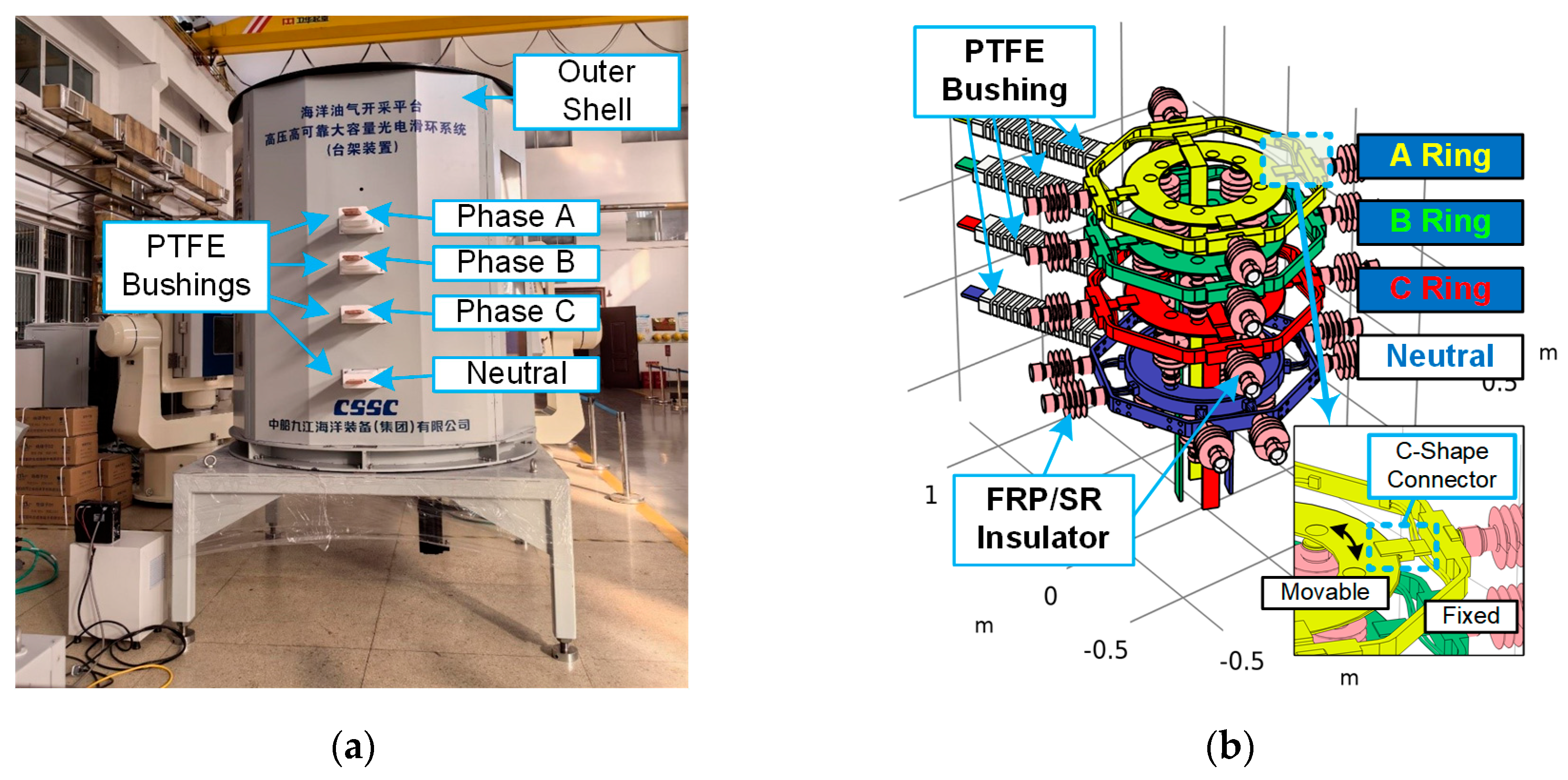
Figure 2.
Geometrical model for electric field calculation in COMSOL software.
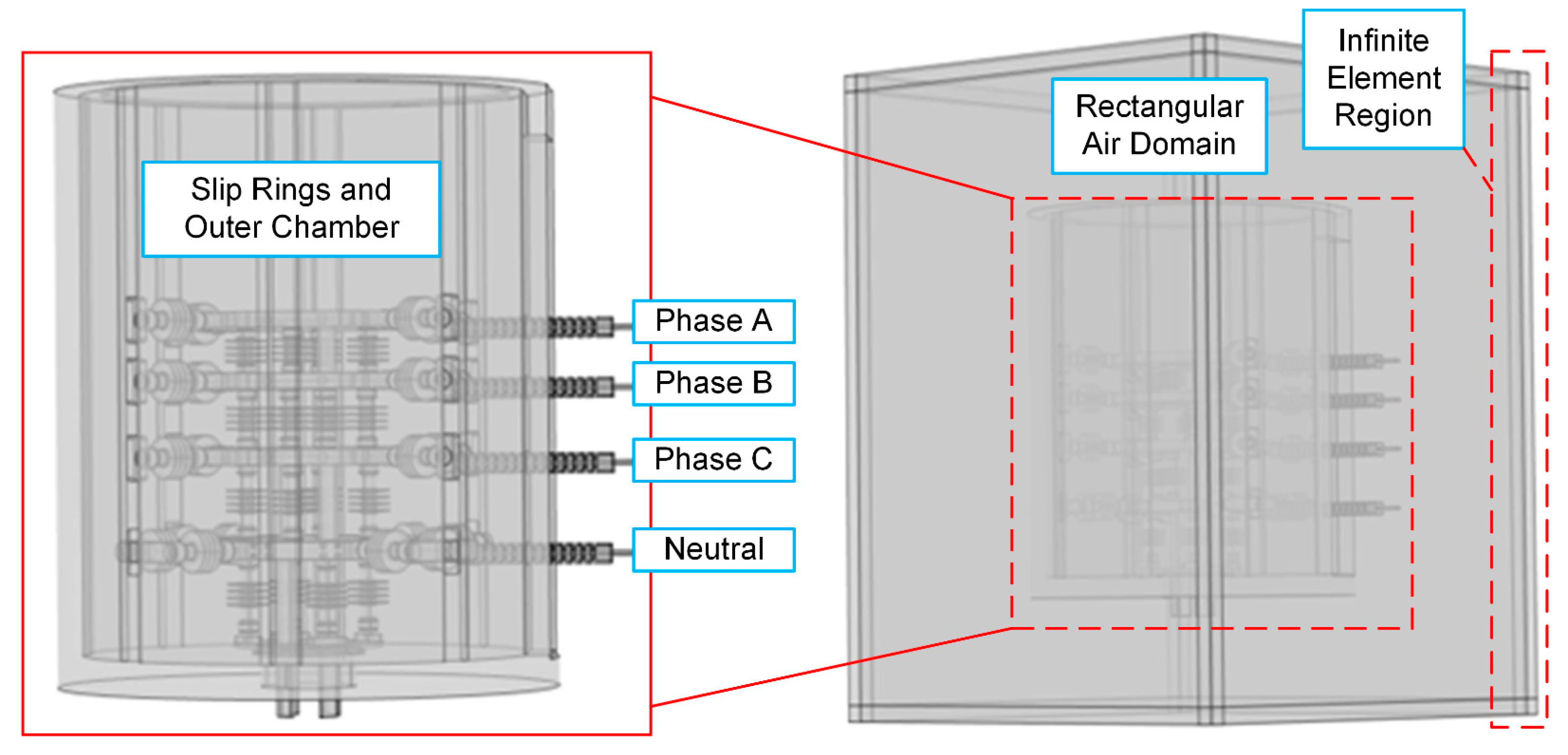
Figure 3.
Conceptual illustration of high voltage and grounding application in the electrical insulation tests, including the test on (a) phase A, (b) phase B, (c) phase C and (d) neutral conductor.
Figure 3.
Conceptual illustration of high voltage and grounding application in the electrical insulation tests, including the test on (a) phase A, (b) phase B, (c) phase C and (d) neutral conductor.
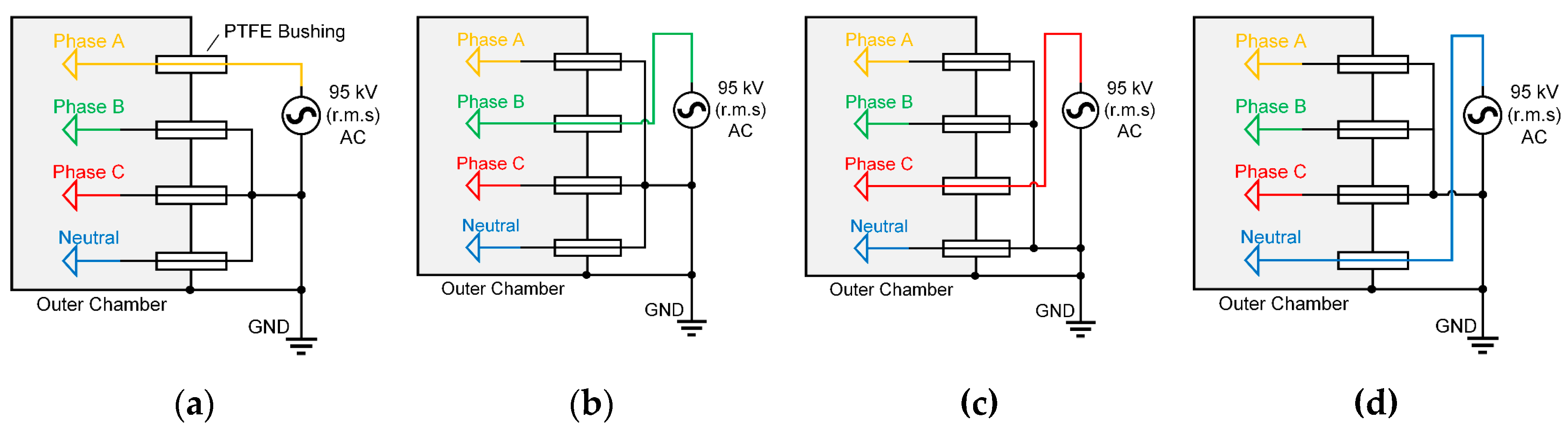
Figure 4.
Structure of the simplified model (i.e., phase A ring) for magnetic-thermal simulation.
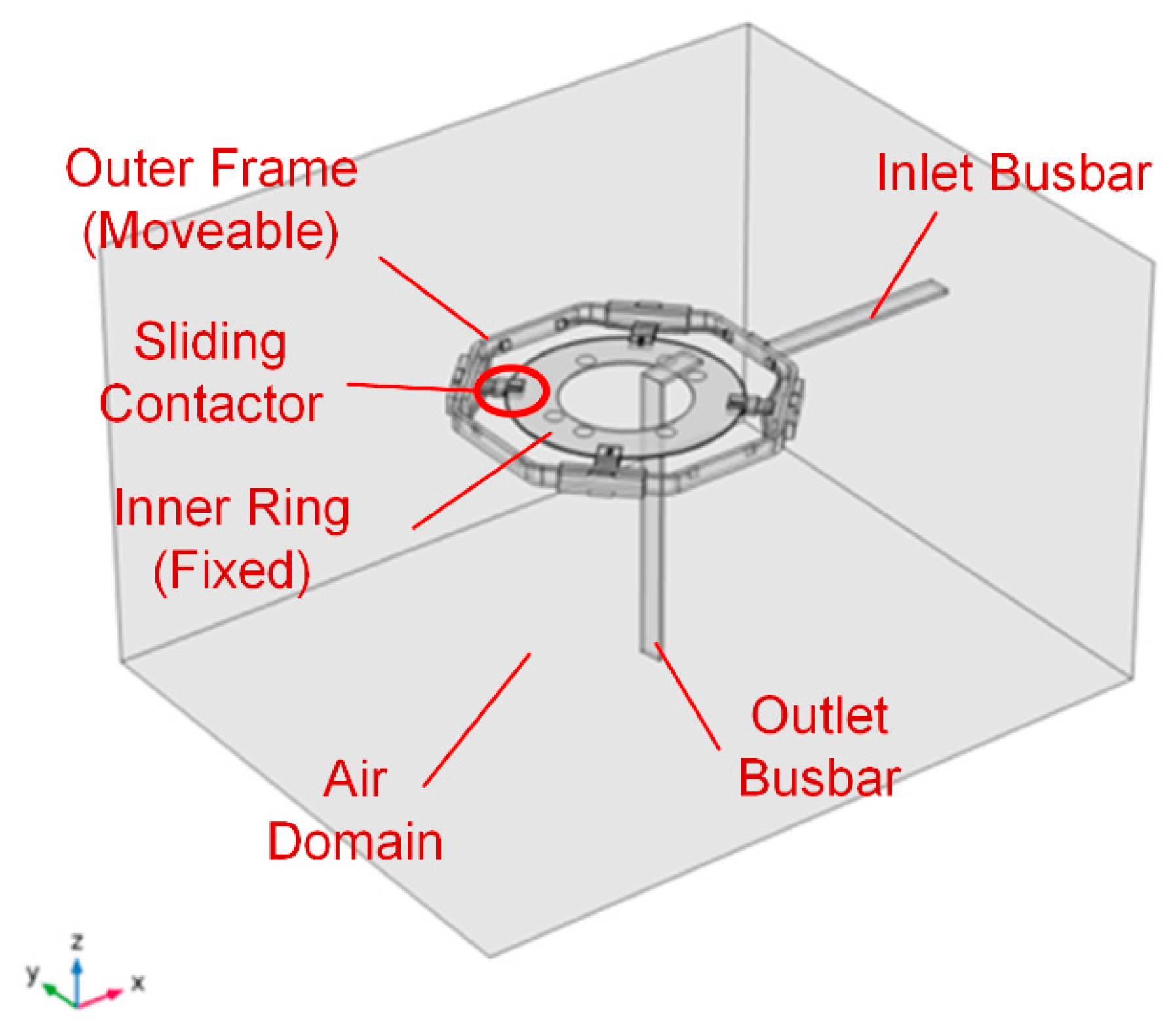
Figure 5.
Electric field distribution on Phase A cut planes when 95 kV r.m.s high voltage is applied on phase A ring, including (a) longitudinal cut plane and (b) vertical cut plane.
Figure 5.
Electric field distribution on Phase A cut planes when 95 kV r.m.s high voltage is applied on phase A ring, including (a) longitudinal cut plane and (b) vertical cut plane.
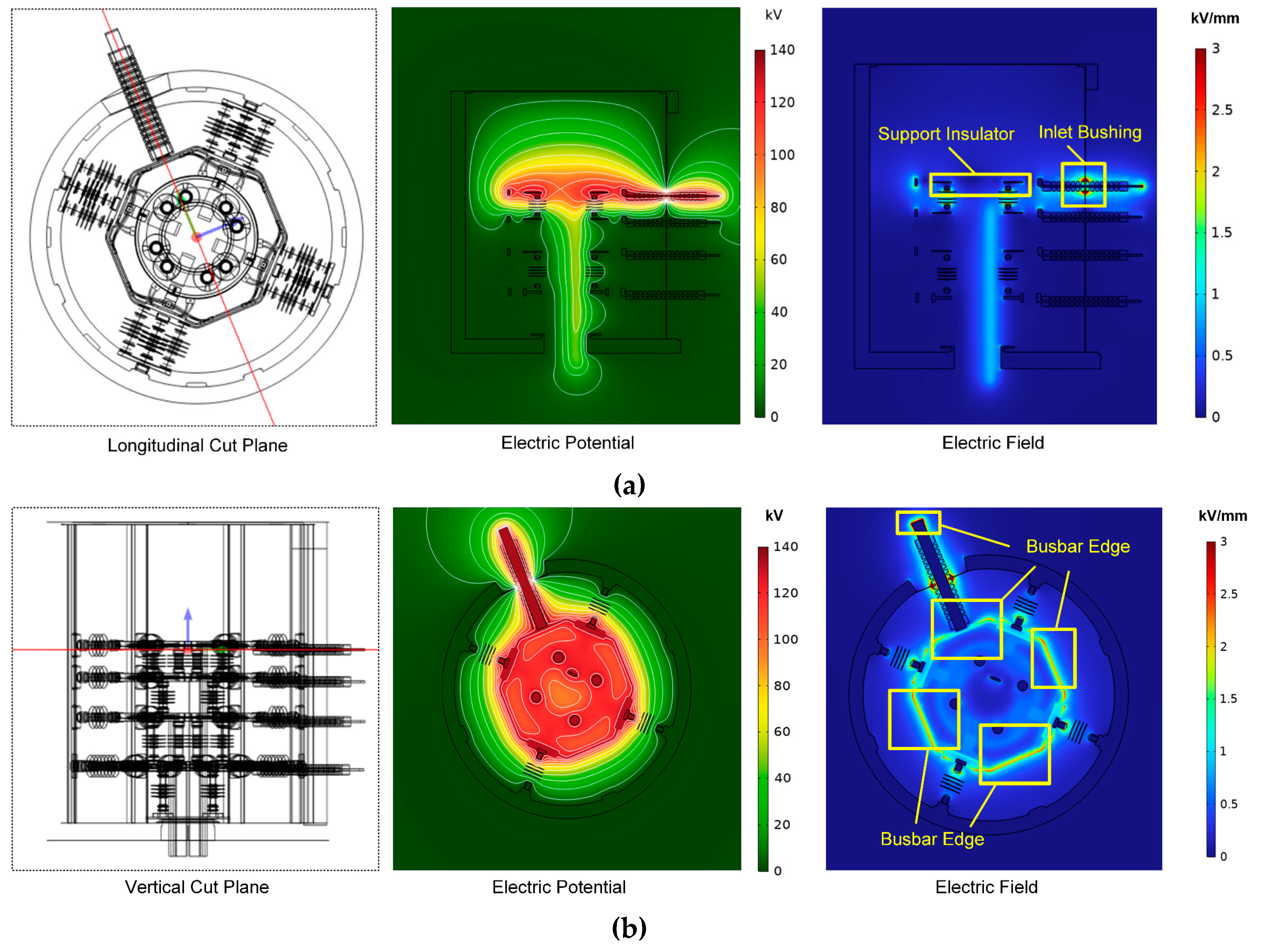
Figure 6.
Electric field distribution and high field region (“red zone”) of the insulation system when 95 kV r.m.s high voltage is applied on (a) phase A ring, (b) phase B ring, (c) phase C ring and (d) neutral ring.
Figure 6.
Electric field distribution and high field region (“red zone”) of the insulation system when 95 kV r.m.s high voltage is applied on (a) phase A ring, (b) phase B ring, (c) phase C ring and (d) neutral ring.
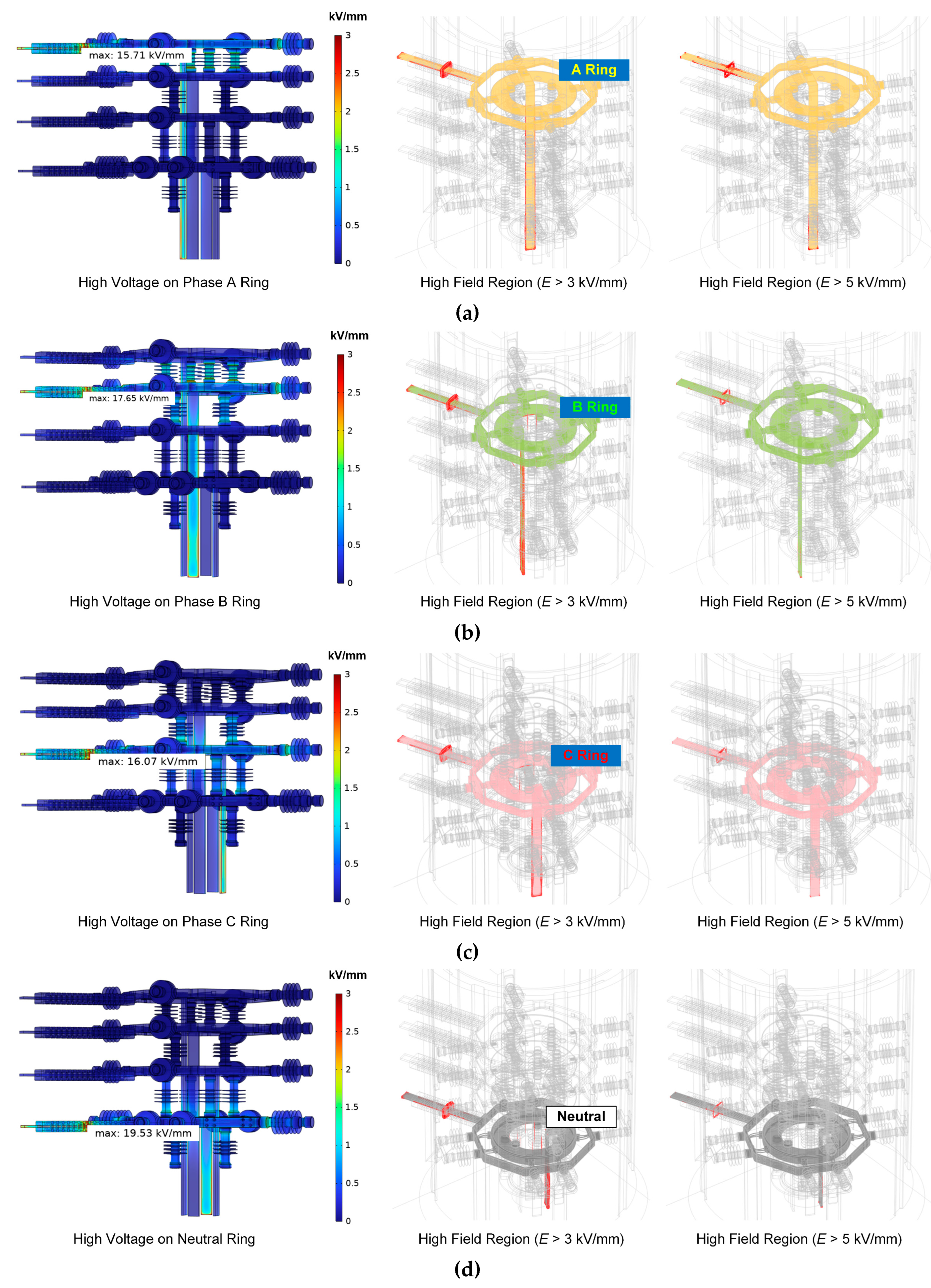
Figure 7.
Steady-state temperature rise on (a) Overall view of the simplified model, (b) Central sliding ring, and the heat flow (blue arrow) inside the copper conductor.
Figure 7.
Steady-state temperature rise on (a) Overall view of the simplified model, (b) Central sliding ring, and the heat flow (blue arrow) inside the copper conductor.
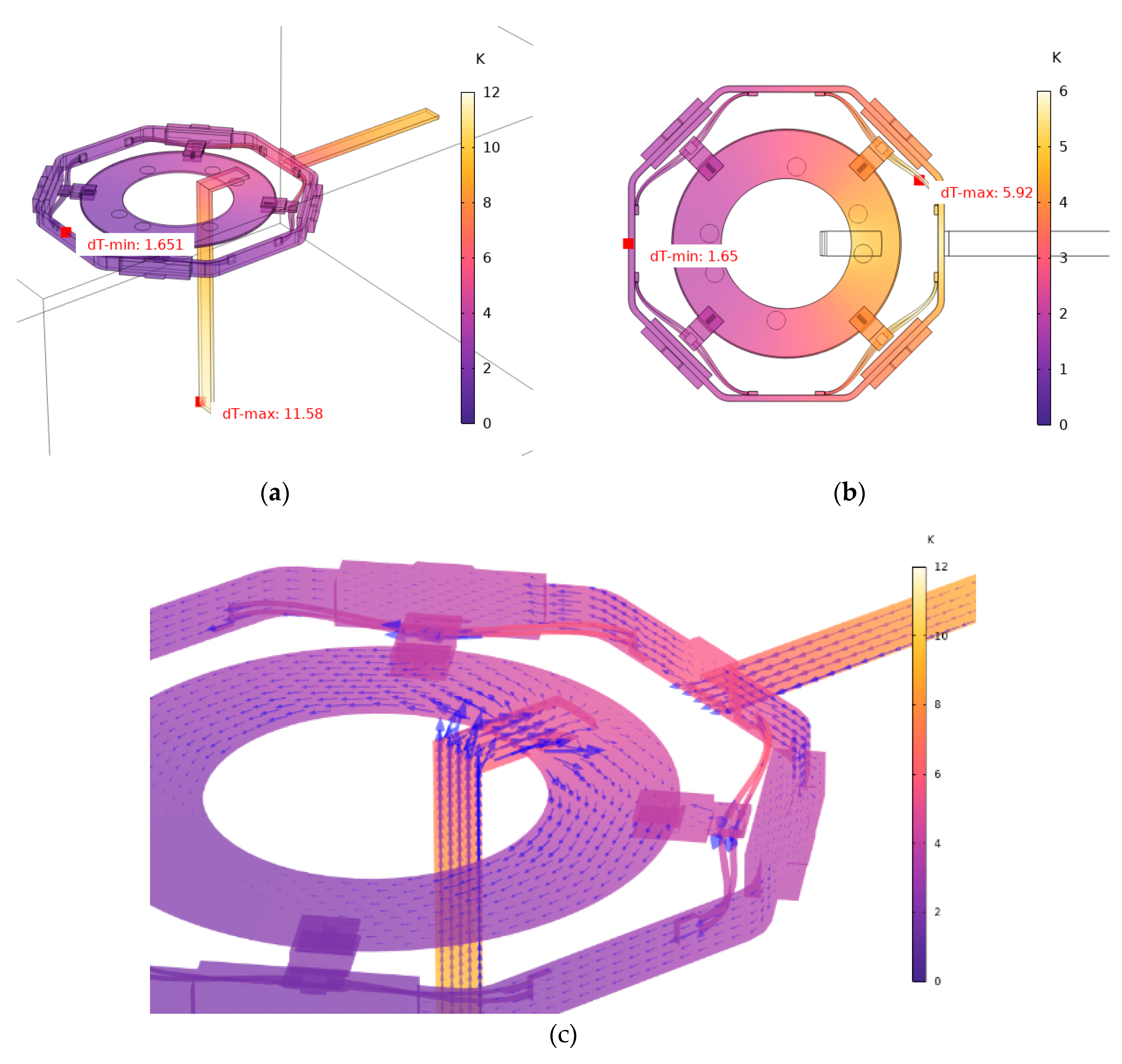
Figure 8.
Current density in the phase A ring at 640 A current under (a) Near-DC(0.01Hz) and (b) AC 50Hz, and in (c) the inlet busbar cross-section at the input port.
Figure 8.
Current density in the phase A ring at 640 A current under (a) Near-DC(0.01Hz) and (b) AC 50Hz, and in (c) the inlet busbar cross-section at the input port.
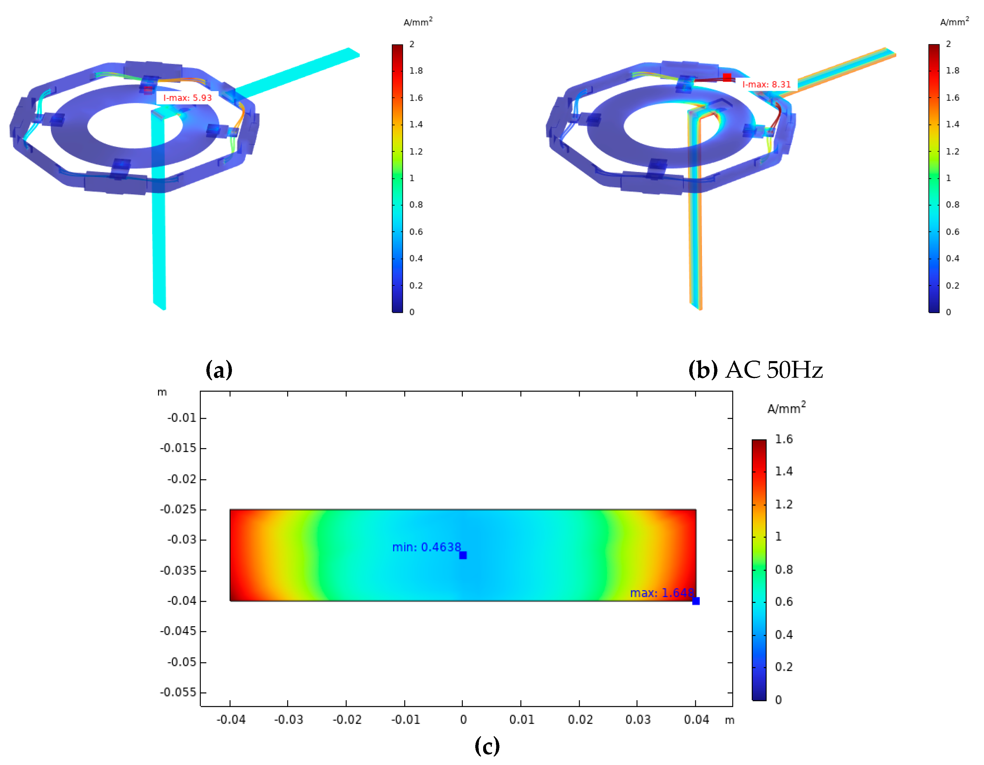
Figure 9.
Temperature Rise of the Central Ring as a Function of r.m.s. Current Load I When the Convective Heat Transfer Coefficient h is (a) h = 1 W·m-1·K-1, (b) h = 2 W·m-1·K-1, (c) h = 5 W·m-1·K-1, (d) h = 20 W·m-1·K-1.
Figure 9.
Temperature Rise of the Central Ring as a Function of r.m.s. Current Load I When the Convective Heat Transfer Coefficient h is (a) h = 1 W·m-1·K-1, (b) h = 2 W·m-1·K-1, (c) h = 5 W·m-1·K-1, (d) h = 20 W·m-1·K-1.
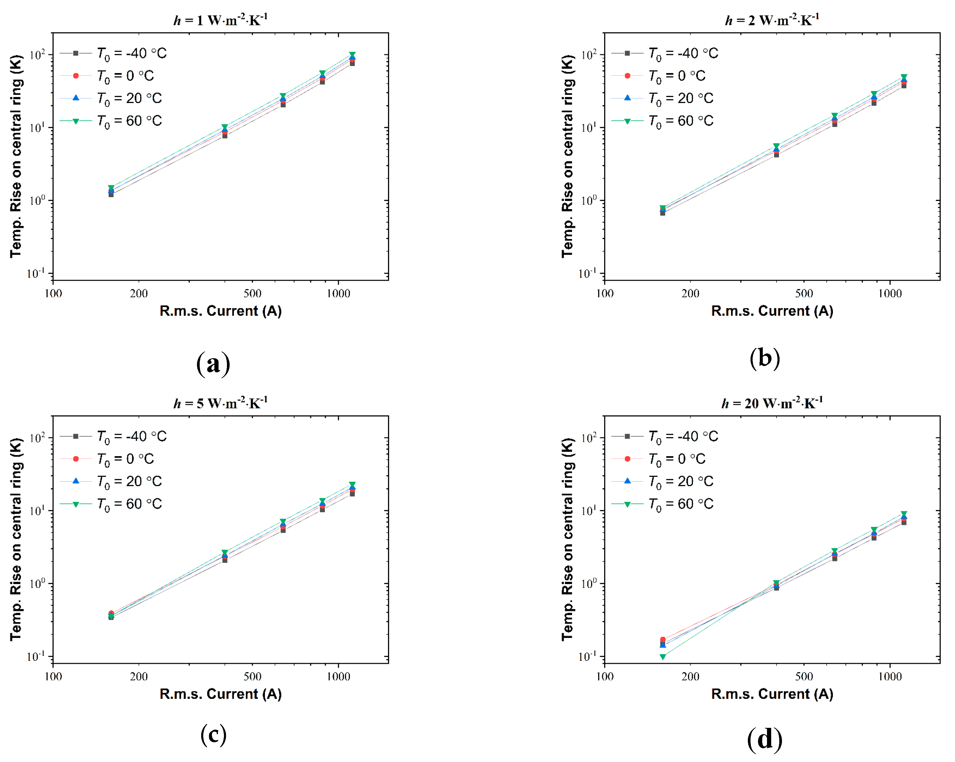
Figure 10.
Temperature Rise of the Central Ring as a Function of Convective Heat Transfer Coefficient h when the r.m.s. Current Load I is (a) I = 160A, (b) h = 400A, (c) h = 640A, (d) h = 1120A.
Figure 10.
Temperature Rise of the Central Ring as a Function of Convective Heat Transfer Coefficient h when the r.m.s. Current Load I is (a) I = 160A, (b) h = 400A, (c) h = 640A, (d) h = 1120A.
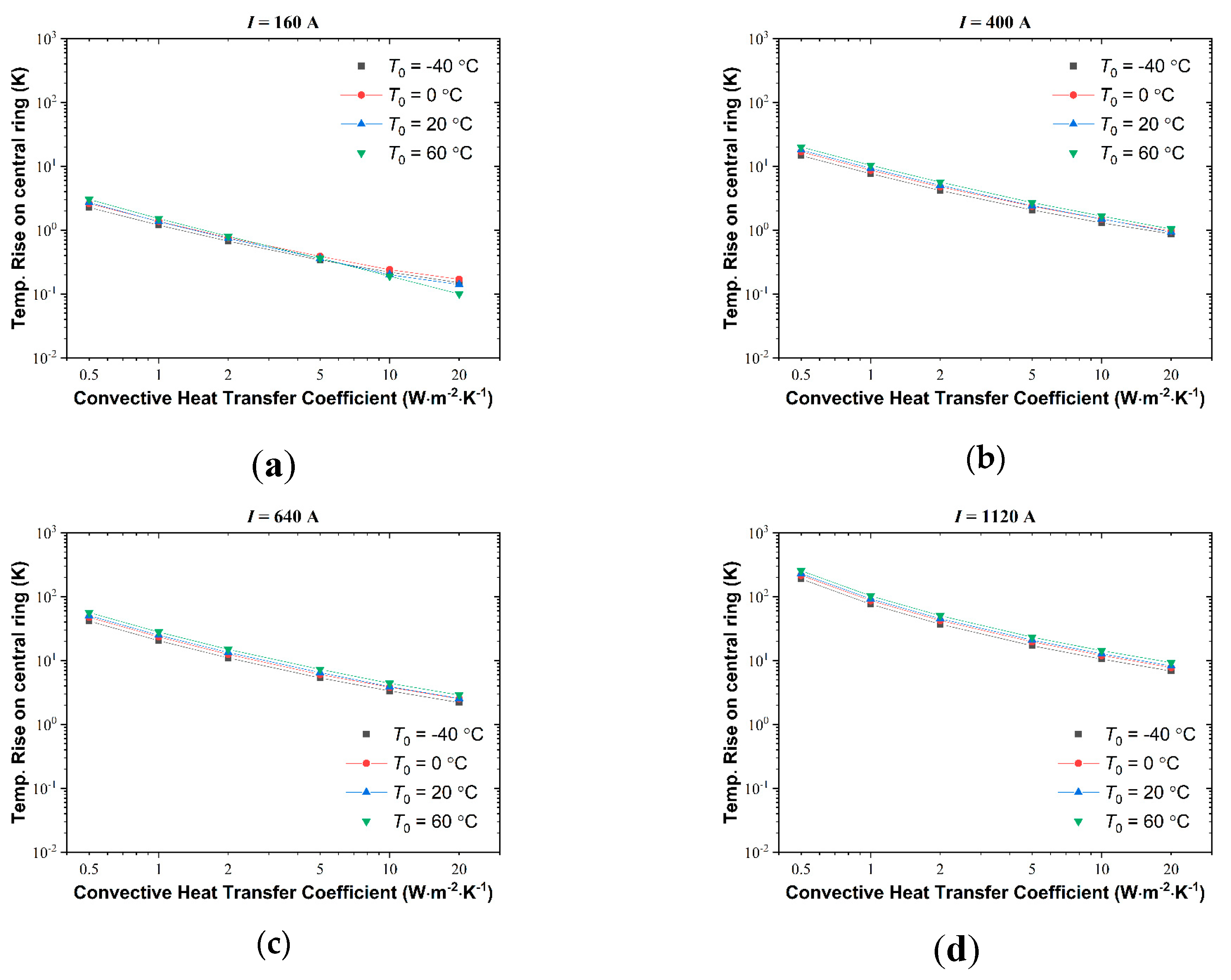
Figure 11.
Temperature Rise of the Center Contact Ring as a Function of Ambient Temperature T0 when the r.m.s. Current Load I is (a) I = 160A, (b) h = 400A, (c) h = 640A, (d) h = 1120A.
Figure 11.
Temperature Rise of the Center Contact Ring as a Function of Ambient Temperature T0 when the r.m.s. Current Load I is (a) I = 160A, (b) h = 400A, (c) h = 640A, (d) h = 1120A.
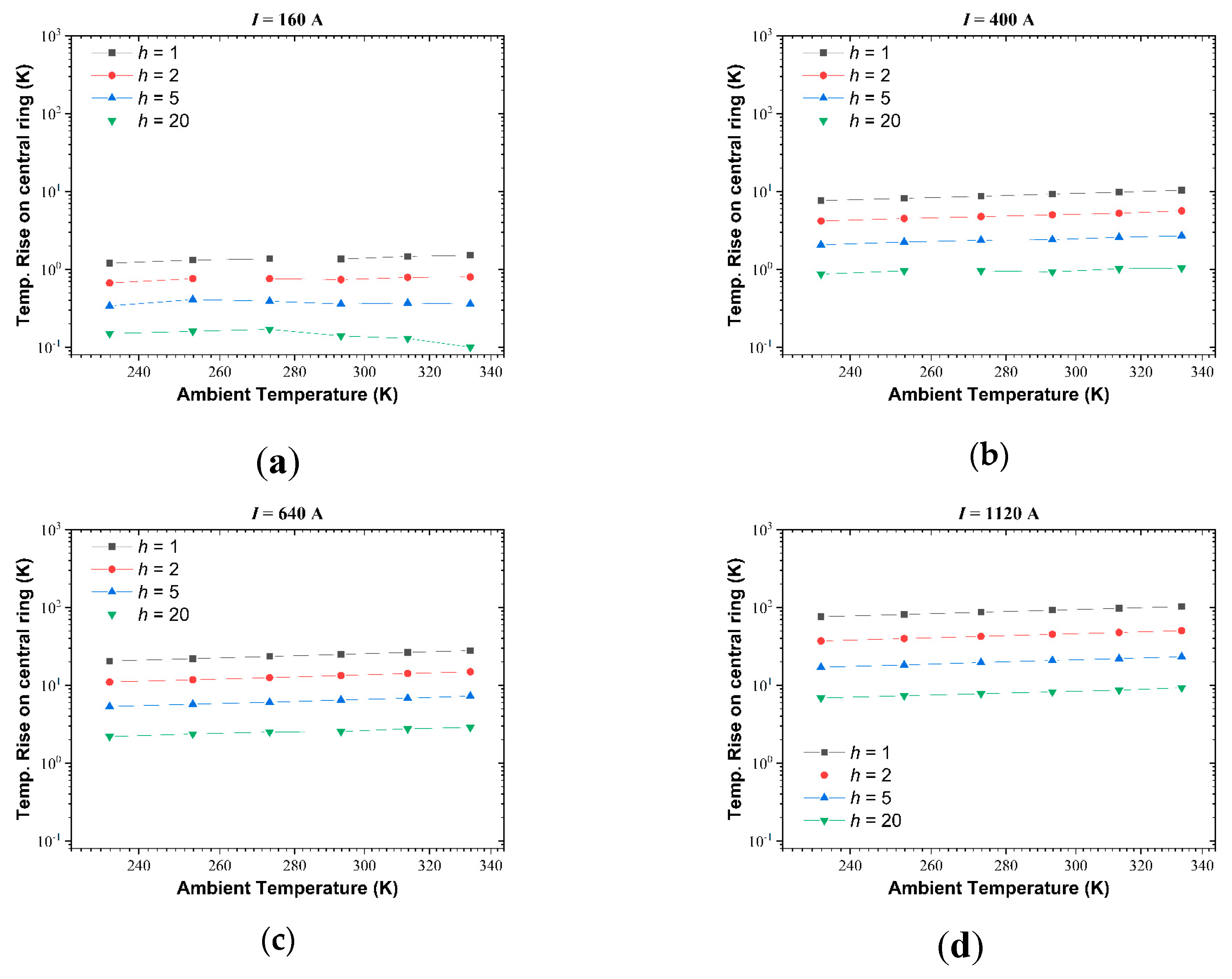
Figure 12.
Experimental configuration for Electric field simulation, including (a) AC withstand test setup for phase A ring and (b) breakdown failure observed at the inlet PTFE bushing.
Figure 12.
Experimental configuration for Electric field simulation, including (a) AC withstand test setup for phase A ring and (b) breakdown failure observed at the inlet PTFE bushing.
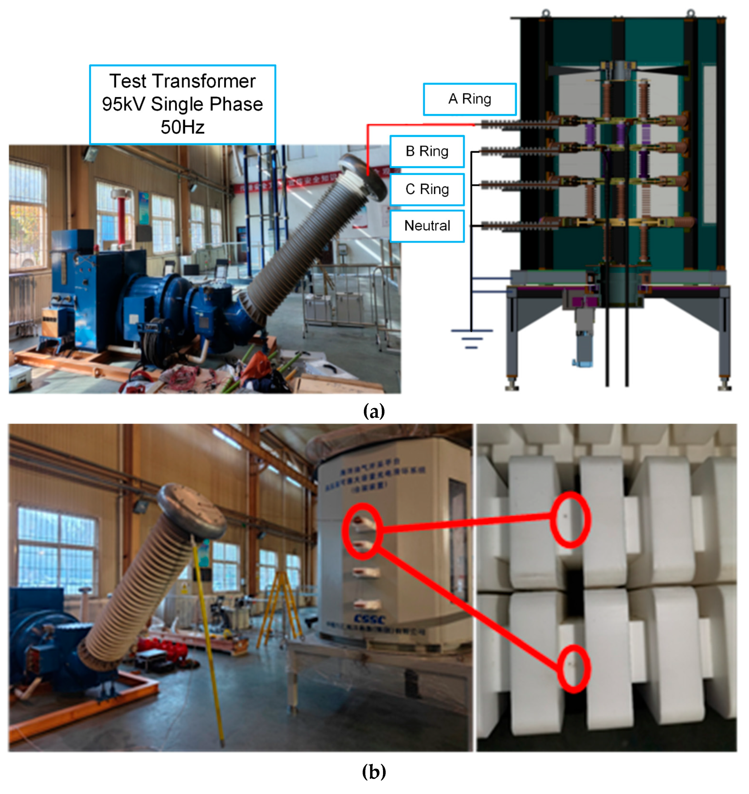
Figure 13.
Experimental configuration for the temperature rising test.
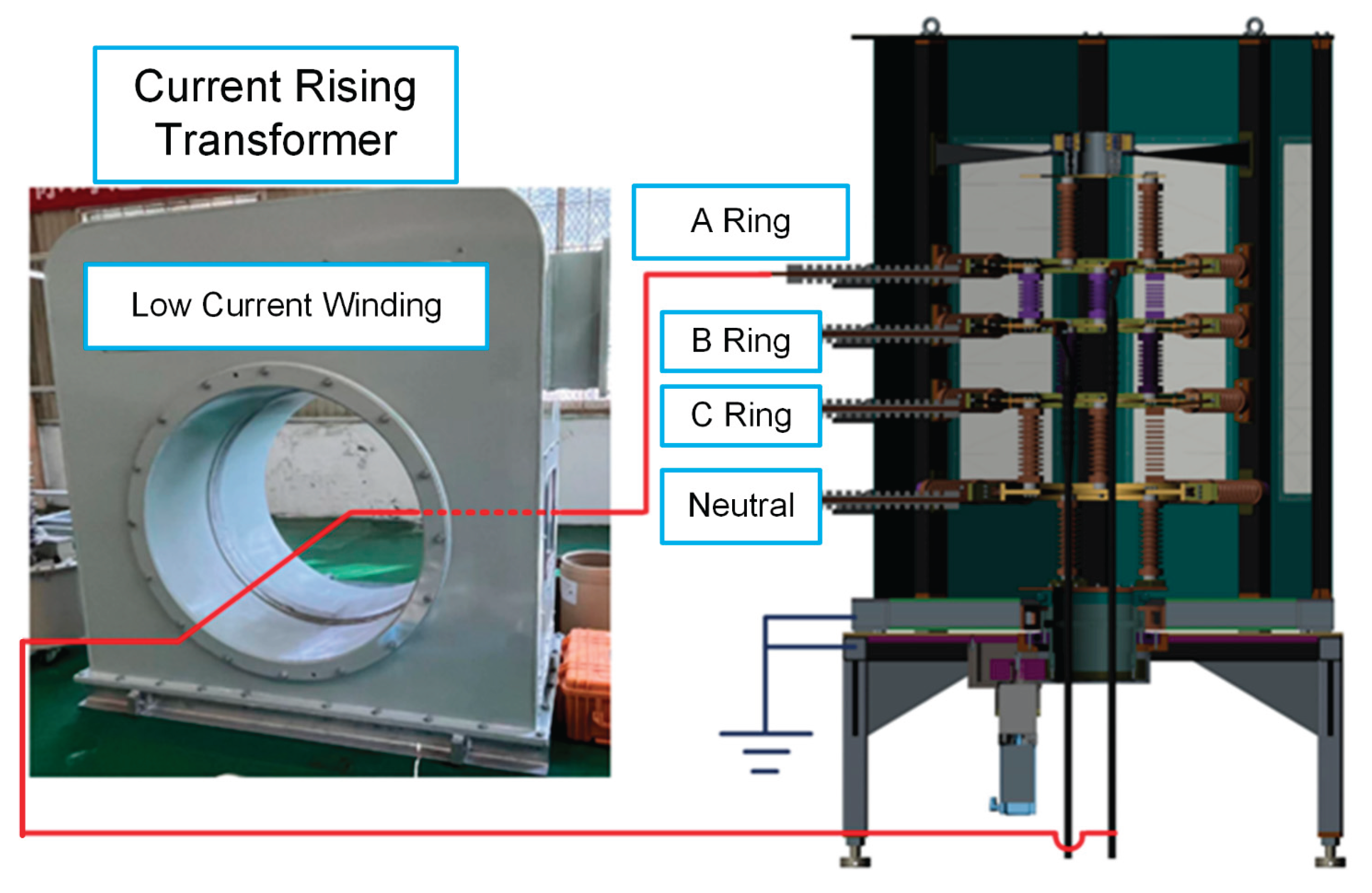

Table 1.
Comparison between dielectric and conductive properties of electrical insulation material in slip ring prototype.
Table 1.
Comparison between dielectric and conductive properties of electrical insulation material in slip ring prototype.
| Material | σ(S·m-1)1 | ωε0εr(rad·F·m-1·s-1)1 |
| Air2 | 10-16 ~ 10-14 | 2.78×10⁻⁹ |
| Glass-Fiber Reinforced Epoxy 2 | 10-14 ~ 10-13 | 1.39×10⁻⁸ |
| Silicone Rubber2 | 10-13 ~ 10-12 | 8.34×10⁻⁹ |
1Dimension formula of σ, ω and ε0 is [M–1 L–3 T3 I2], [T-1] and [M–1L–3T4I2], respectively. The relative permittivity εr is dimensionless. Therefore, σ and ωε0εr has identical dimension formula [M–1 L–3 T3 I2] and indicate same physical quantities (although the literal form is different). 2The relative permittivity of air, epoxy rod and silicone rubber are chosen as 1.0, 5.0 and 3.0 respectively. The frequency f is 50Hz.
Table 2.
Dielectric parameters of electrical insulation material in slip ring prototype.
| Material | Relative Permittivityεr |
| Metal Conductor (steel and copper) | 1.0 × 10⁶ |
| Air | 1.0 |
| Supporting insulator | 4.0 |
| PTFE bushing | 2.2 |
Table 3.
Material parameters related to thermal simulation in slip ring prototype.
| Material | Electrical Conductivity σ (S·m-1) | Magnetic Permeability μ |
Thermal Conductivity k(W·m-1·K-1) |
| Air | 1×10-18 | μ = μ0= 4π×10-7 H·m-1 | 0.0257 |
| Copper | Equation (20) | 398.9 |
Table 4.
Test results of AC breakdown experiments.
| Test Conductor | Maximum electric field in Simulation (kV/mm) | AC breakdown voltage (kV) | Position of breakdown |
| Phase A ring | 15.71 | 75.2 | Inlet PTFE bushing |
| Phase B ring | 17.65 | 68.0 | |
| Phase C ring | 16.07 | 72.2 | |
| Neutral ring | 19.53 | 55.8 |
Table 5.
Comparison between simulated and experimental temperature rise.
| Current (A, r.m.s.) | Simulated ΔT (K) | Measured ΔT (K) | Error (%) |
| 160 | 0.50 | 0.54 | -13.7% |
| 400 | 3.15 | 3.42 | -7.9% |
| 640 | 8.22 | 7.99 | 2.9% |
| 880 | 16.09 | 15.3 | 5.2% |
| 1120 | 26.77 | 24.85 | 7.7% |
Disclaimer/Publisher’s Note: The statements, opinions and data contained in all publications are solely those of the individual author(s) and contributor(s) and not of MDPI and/or the editor(s). MDPI and/or the editor(s) disclaim responsibility for any injury to people or property resulting from any ideas, methods, instructions or products referred to in the content. |
© 2025 by the authors. Licensee MDPI, Basel, Switzerland. This article is an open access article distributed under the terms and conditions of the Creative Commons Attribution (CC BY) license (http://creativecommons.org/licenses/by/4.0/).
Copyright: This open access article is published under a Creative Commons CC BY 4.0 license, which permit the free download, distribution, and reuse, provided that the author and preprint are cited in any reuse.


