
Submitted:
24 November 2025
Posted:
26 November 2025
You are already at the latest version
Abstract
Surface-enhanced Raman scattering (SERS) is a highly sensitive analytical technique capable of single-molecule detection, owing to its exceptional chemical specificity, sensitivity, and reproducibility. In this study, we developed a robust SERS platform based on long-range ordered bullseye plasmonic nano-gratings, fabricated via a combination of electron beam lithography and reactive ion etching. The resulting nanostructured arrays—comprising concentric bullseye patterns with tunable period and filling fraction—were uniformly coated with a thin gold film to support strong surface plasmon resonances, generating intense electromagnetic field enhancements across the substrate. Using this platform, we demonstrated quantitative detection of small molecules such as Rhodamine 6G at low concentrations, achieving enhancement factors on the order of 105. Interestingly, we found that the geometric configuration yielding the strongest local electric field did not correspond to the highest SERS enhancement, which we attribute to a mismatch between the field orientation and molecular polarizability alignment. This study provides insights for optimizing plasmonic substrates for sensitive molecular detection.
Keywords:
surface-enhanced raman scattering (SERS)
; bullseye plasmonic nano-gratings
; localized surface plasmons (LSPs)
; surface plasmon polaritons (SPPs)
; electromagnetic field enhancement
; plasmonic substrate optimization
1. Introduction
Raman spectroscopy is a powerful, non-destructive, and highly sensitive analytical technique capable of providing molecular fingerprinting as well as structural, chemical, mechanical, and thermal information about a sample [1]. However, its widespread application is limited by the inherently weak signal resulting from the inelastic nature of Raman scattering [2,3]. To overcome this limitation, surface-enhanced Raman spectroscopy (SERS) has been developed, leveraging surface plasmon polaritons (SPPs) to confine, enhance, and localize optical fields at subwavelength scales [4]. Direct excitation of SPPs on smooth metal surfaces is hindered by the wavevector mismatch between incident light and surface modes [5]. Therefore, coupling mechanisms such as prisms, waveguides, optical fibers, or gratings are required to facilitate SPP excitation [6]. Prism-based approaches are more commonly used [7,8,9,10], but the bulky nature of prism-based systems limits their integration into compact or portable sensing devices. By contrast, gratings are particularly attractive due to their high coupling efficiency, compatibility with normal incidence, and tunable optical response through precise control of geometric (period, height, width) and material parameters [11,12,13].
Previous studies have investigated periodic rectangular and sinusoidal gratings for SPP-assisted Raman enhancement [14,15,16,17,18]. However, research on circular grating–where the grooves form concentric rings resembling a "bullseye" pattern–remains limited. In particular, the influence of the grating period (defined as the sum of groove width and spacing) and the filling fraction (the ratio of groove width to period) on the localized electric field and the resulting Raman enhancement factor (EF) has not been thoroughly explored.
Literature suggests that this geometry holds great potential for SERS, as it has already demonstrated efficient SPP generation in other application fields [19,20,21]. The pioneering work by Lezec et al. demonstrated substantial transmission enhancement through a subwavelength aperture using a bullseye geometry, attributed to the efficient excitation of surface plasmon resonances [22,23,24]. Since then, plasmonic bullseye antennas have been successfully employed in enhanced transmission, energy concentration, beam steering, and polarimetry [25,26,27,28], with analogous microwave leaky-wave antenna designs achieving similar functionalities for high-gain, low-profile communications systems [29,30,31].
In the present work, we carried out a careful SERS investigation on a gold-coated bullseye grating. We examined the impact of the array geometry, especially the change of period and filling fraction, on the SERS EF. For this purpose, fifteen unique structures with variations in period and filling fraction were fabricated using the combination of electron beam lithography (EBL) and reactive ion etching (RIE), followed by metallization with gold. Dependences between period, filling fraction, and SERS enhancement factor were studied from theoretical and experimental points of view. High sensitivity and quantitative detection ability are simultaneously obtained in bullseye SERS substrates. A low SERS detection limit of M for Rhodamine 6G is realized with EF at . The relative standard deviation is 2.1%-2.9%. Even in a broad concentration range from to M, the SERS intensity and concentration relationship can be fitted as a sigmoidal curve with .
2. Optical Properties and Physical Background
To excite an SPP, energy and momentum need to be transferred from a photon or light to the free electron at the interface, resulting in collective oscillations; thus, the momentum must be conserved. The momentum is highly dependent on the dielectric constant (permittivity) of both metal and dielectric materials. In this study, the system is built by a semi-infinite air above a gold-silicon interface (the thickness of the gold is 40 nm). The optical properties of this interface were calculated, and the results are shown in Figure 1a. The permittivity was calculated based on the refractive index (n) and extinction coefficient (k) of each material; the corresponding literature values for the near-infrared region are taken from Johnson and Christy’s data [32]. The permittivity, represented as a complex number , indicating the interface’s response to electric field. A high negative real part of the permittivity indicates that the material supports collective electron oscillations that lag behind the driving field due to electron inertia–an essential condition for plasmonic resonances to happen. The imaginary part of the permittivity quantifies how lossy a material is, representing energy absorption due to internal damping. The imaginary part means a high loss (absorption).
For better quantification, two types of quality factor (Q factor) can be calculated: they are surface plasmon polariton () and localized surface plasmon resonance (), both illustrated in Figure 1b. The corresponding equations are valid for interfaces of metal and air [4].
Although a high value of correlates with a strong observable plasmon resonance, can be used to calculate the propagation length for SPPs at a given wavelength. The propagation length is given by,
where c is the incident light speed in vacuum and is the angular frequency of the photon or incident light [33]. Figure 1b shows large values for QSPP, which has low loss and longer propagation length (∼43 m as shown in Figure S1), therefore, gold can be considered a promising candidate for observing SPPs.
The SPP propagation constant at a planar metal-dielectric interface is always larger than light for any given frequency. This wave vector mismatch is represented in Figure 1c, where k is the propagation constant, and frequency is the angular frequency (). The dispersion curves of the SPP mode in air-gold and in gold-silicon interface are plotted. The intersection between the core mode and the SPP mode dispersion curves determines the phase matching condition. There is no intersection, thus, an additional momentum needs to be added to the momentum of the incident optical wave to match that of the SPPs. The coupling of light to SPPs can respond to light scattering at periodic patterned surfaces, which provides the incident wave with an additional momentum.
A grating at this gold-silicon interface is required to couple light from a laser pulse to SPP. The surface plot in Figure 2 depicts the simulation results of the reflectance spectra calculated for a grating at the gold-silicon interface (width = 100 nm, period = 200 nm, depth = 100 nm) in terms of incident angle and light wavelength. The simulation was set at various incident angles from -30° to 30° normal to the grating surface, and wavelength from 600 nm to 1100 nm, corresponding to a frequency shift from 2 Hz to 5 Hz. Through the calculation, as the light doesn’t go through, which decay rapidly inside the substrate, the transmission is set to zero (Figure S2a), the weak intensity (dark purple) area of the reflected light indicates that for a certain combination of wavelength and incident angle, the reflected light is minimized might cause by the excitation of SPPs at the metal surface.
The SPP dispersion curve of the grating is shown in Figure S2(b). Compared to the flat interface, the grating dispersion curve becomes more curved (higher group velocity) as it introduces momentum states as . The group velocity then can be determined from the angular frequency () with respect to its propagating constant (), or , where ; and is the wavelength and is the incident angle, c is the light speed ( m/s). We can calculate group velocity in the range of visible light (shown in Figure S2(c-d)); the group velocity is about 9.5 m/s, slower than the speed of light. This occurs when the light interacts with the interface, leading to collective oscillation of surface electrons, with energy transferred to the metal surface and the light slowing down.
3. Results and Discussion
Gold-coated bullseye grating arrays were fabricated by a combination of electron beam lithography (EBL) and reactive ion etching (RIE), followed by e-beam gold deposition. The structure has four concentric annular grooves milled into a silicon substrate to a depth of 150 nm using the combination of electron beam lithography and reactive ion etching. Dimensions characterizing the grooves and holes lie in the subwavelength regime (wavelength = 785 nm): all grooves have a depth of 150 nm, and the central hole has a radius of . The normalized period is chosen from 0.33 to 1.53 and is calculated by , where is the normalized period, is the physical period defined as the sum of the groove width and the spacing to the nearest groove, is the incident wavelength, and is the effective refractive index. The effective permittivity can be written as , where f is the filling fraction (or duty cycle), set from 0.2 to 0.8 and defined as the groove width divided by the physical period. The normalized period is used to account for different materials through the use of an effective refractive index. The number of annular grooves is set to on each side, which is sufficient to achieve field enhancement. The entire structure is coated with a gold film of thickness 40 nm (a 10 nm titanium adhesion layer is deposited by e-beam evaporation prior to gold deposition). The surface roughness is controlled by tuning the deposition current and rate. The structural unit of the substrate consists of bullseye nanostructures spaced 200 nm apart, forming a long-range ordered array in a rectangular arrangement (Figure 3a–c).
Employing Rhodamine 6G (R6G) as the probe molecule in the range of M to M, we obtained a complete molecular vibration spectrum characterized by distinct and sharp peaks (Figure 3d). R6G is a highly fluorescent rhodamine family dye, which is widely used to determine SERS behaviour. The characteristic Raman peaks of R6G at 773 cm−1 and 1183 cm−1 were assigned to the out-of-plane vibrations and in-plane vibrations of the C-H bond, respectively [34]. The bands at 1310 cm−1, 1360 cm−1 1505 cm−1, and 1604 cm−1 can be attributed to the aromatic C-C stretching vibration modes [34].
It is noted that as the concentration of R6G decreases, the SERS intensity at 1310, 1360, and 1505 cm−1 gradually decreases (Figure 3e), which exhibits a linear relationship between Raman intensity and concentration for all three peaks, with a coefficient of determination (R2) up to 0.96. Additionally, from Figure 3f, ten different random spots were used to acquire Raman spectra of the R6G at a concentration of 10−3 M; the average relative standard deviation of all three highest characteristic peaks is between 2.1% and 2.9%, indicating good signal uniformity from the substrates.
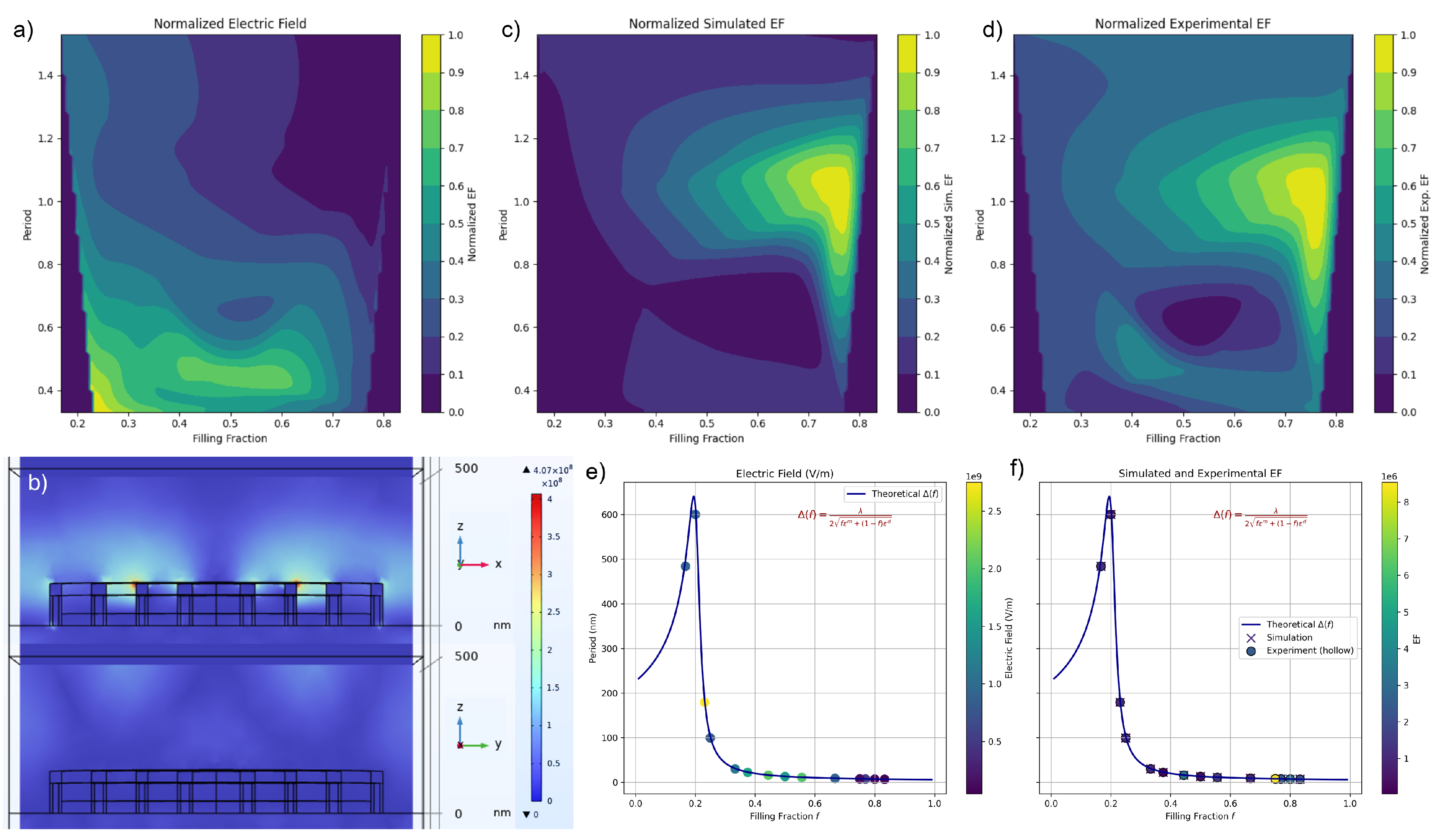
From the Raman spectra, we clearly see that the bullseye structure can enhance the Raman signal dramatically. To better understand the physics of plasmonic enhancement and optimize SERS performance, we then modelled electric fields of different geometries using the finite element method (FEM), with Figure 4b showing one geometry as an example. We considered a 500 nm air layer (n = 1) above the gold layer. Since the bullseye is a periodic array, we modeled it by using periodic boundary conditions along the direction of periodicity. The grating was illuminated from the top of the model window at a normal incidence. The illumination was a linearly transverse magnetic (TM) polarized wave. The electric field forms only on the x-z plane due to p-polarization, with no component in the y-direction. Consequently, the strong electric field is confined at the sharp edge of the groove and in the nanogap.
SPPs are excited through the interaction of the incident light with the gold grating-air interface, generating electric field confinement as illustrated in Figure 4b. Therefore, the goal is to optimize the SPP resonance matching with a 785 nm adsorption wavelength. The phase matching condition of SPP coupling on a grating is,
where is the momentum in free-space or vacuum, which is , is the wavelength of light in vacuum; n is the integer of the diffraction order. In this study, we only discuss n = 1 and n = -1, where the brightest diffracted beams (or fringes) are observed, is the incidence angle, is the 785 nm excitation wavelength, and is the grating period. To study the period and filling fraction isolated dependent electric field at a wavelength of 785 nm, we varied the period and filling fraction of the grating from 0.4 to 1.4 and 0.2 to 0.8, respectively, as shown in Figure 4a. Noticed here, the electric field intensity is normalized against the maximum value of 4.45 V/m – 2.75V/m to 0 – 0.99 to facilitate comparison. The period is also normalized (more details can be found in experimental information) to minimize the effect of varying the metal-to-air ratio in plasmonic gratings. As a result, at the electric field maximum, reducing the grating period increases grating momentum , which allows phase matching at lower angles. A smaller filling fraction means a narrower groove; the material loss can be reduced, allowing more efficient energy buildup in the plasmonic mode.
From Figure 4c,d, we found that the choice of the grating period and filling fraction can significantly impact the electric field strength; thus, it should also impact the electric field-induced surface-enhanced Raman scattering performance. To compare, one must consider the enhancement factors (EFs). The EFs in experiments were calculated using a commonly used 3,
where, and denote the characteristic peak intensities collected over the SERS platform and on the flat gold platform, respectively. and are the number of scattering probe molecules on the SERS platform and the flat gold platform in the region of the laser spot, respectively.
It should be noted that the is one order-of-magnitude larger than . Ragheb et al. mention that a chemical contribution to the Raman gain may contribute to two orders of magnitude difference [35]. Such discrepancy has also been pointed out by Chu et al., who noted similar differences between simulation and experimental EF values, attributed to fabrication imperfections [36]. After normalization to its maximum, both EFsimulation and EFexperiment show a similar trend, both maximums correspond to period at 1, given Equation 4. Also note that very high enhancement at high filling fractions is due to the very high energy density confined to the gap at high filling fractions [37]. Thus, the phase-matching condition is given [38,39],
Equation 4 shows the critical period () versus filling fraction (f), where light incidence wavelength is 785 nm, is the gold permittivity and is the air permittivity shown in Figure 1a at 785 nm. The dependence of the dielectric constant on the wavelength () arises from material and waveguide dispersion. We then overlaid data points from previously simulated geometries onto this theoretical curve. These geometries align closely with the prediction, and the color of each point represents the strength of the local electric field or enhancement factor (Figure 4 e–f).
When comparing Figure 4e,f, it becomes evident that the bullseye structure exhibiting the highest local electric field strength does not necessarily correspond to the maximum Raman enhancement. This discrepancy arises because enhancement is influenced by both electromagnetic (EM) and chemical mechanisms. While EM enhancement—primarily due to field localization—can contribute enhancement factors (EF) exceeding 104, the chemical mechanism (CM), which depends on molecular orientation and polarizability, typically contributes much smaller enhancements ().
where is the enhancement sigbal, is the enhanced local electric field near the nanostructure due to plasmonic effects, and is indicating which direction in space the molecular polarizability changes most when that vibration occurs. If and are aligned, their dot product is maximized, then the enhancement is strong; their dot product is maximized, resulting in strong Raman enhancement. If they are orthogonal, the dot product is zero, and the enhancement is suppressed.
To assess this alignment, we examined how the electric field direction—controlled by nanostructure geometry—overlaps with the orientation of the R6G molecule. We found that bullseye structures with higher filling fractions (around 0.8) produce more vertically oriented electric fields (Figure S3), which better match the known vertical orientation of R6G on gold surfaces. Ujihara et al. reported that R6G molecules adsorbed on Au nanoparticles are predominantly oriented perpendicular to the surface [40], and Moretti et al. observed similar upright orientations on nanostructured gold substrates [41]. This vertical alignment enhances the coupling between the transition dipole moment of R6G and the local field, leading to stronger Raman signals. Thus, optimizing SERS performance requires not only maximizing the electric field strength through nanostructure design but also aligning the local field direction with the molecular orientation to fully exploit both electromagnetic and chemical enhancement mechanisms.
4. Experimental Details
4.1. Electromagnetic Field Simulations
Plasmonic “bullseye” gratings were modelled and optimized using the finite-difference time-domain (FDTD) method implemented by Lumerical FDTD Solutions. This method has been widely used to solve Maxwell’s equation in complex geometries, which can simulate the electromagnetic field on plasmonic metal surfaces. FDTD is a time domain technique with E(t) and H(t), where H is the magnetic field and E is the electric field. The details of the simulation setup are described as follows:
- Define the physical structure: a model is created for each fabricated structure based on dimensions obtained from AFM and SEM image analysis. In this simulation setup, the bullseye grating (in air), was considered as four concentric annular grooves milled into a silicon substrate for 150 nm with a central hole at = 50 nm coated with continuous gold (upper and bottom coated 40 nm and sidewall 10 nm). The normalized period is chosen from 0.33 to 1.53 calculated by , where is the normalized period, is the physical period defined as the sum of groove width and the distance between the nearest groove, is the incident light wavelength and is the effective refractive index. Different filling fractions (or duty cycles) from 0.2 to 0.8 were considered, which are defined as f = width/.
- Define a simulation region and boundary conditions: set a reasonable mesh size, mesh refinement around the rings and cavities are used with a mesh size of 0.04 nm. Also, adjust the mesh size first in the reasonable direction or geometry. Then, periodic boundary conditions (PBCs) are considered along both the x-direction and y-direction, and perfectly matched layer (PML) boundary conditions with a steep angle profile are selected along the z-direction. Ideally, PML boundaries can absorb all incident light without creating any back reflection.
- Define a source of light: the incident light, a Gaussian beam of wavelength, propagates along the Z-axis to excite the system with an amplitude of 1 and a phase of 0. To re-scale the electric field strength in V/m, E was calculated by , where c is the light speed, is the permittivity of free space and I is P/A, power of input is 1 W and the area of the laser focus is 121 m2.
- Define monitors to record data for analysis: the analysis was performed by considering the “Palik” dispersion curve for silicon (Handbook of Optical Constants of Solid E.D. Palok, 1998), whereas the refractive index of titanium and gold is taken from CRC handbook (W.M. Haynes, CRC handbook of chemistry and physics, 95th, Editi, 2014).
The same 3D modeling task was also performed using Finite Element Analysis (FEM) with COMSOL Multiphysics 6.3. As a direction solution in the frequency domain instead of the time domain, it can also obtain a similar solution by exploiting the Fourier transforms. The model was built using Electromagnetic Waves, Frequency Domain, and the geometrical parameters were set the same as FDTD. The background field refractive index (n) was set as 1 (normal background), the wave intensity (k) was set as , the physical field was a scattering field, and the incident field E0 was set as 1 V/m with the z-axis incidence and the x-direction polarization. The periodic boundary was set to the unit cell in the x and y directions to simulate an infinite repeating pattern in both directions. For the z direction, PMLs were added top and bottom.
Simulations were conducted on a single computer with an Intel i7-12700 CPU with 12 cores and 128 GB RAM. Depending on the geometry, simulations took from 30 minutes to 20 hours real time to reach converged solutions.
4.2. Fabrication
Fabrication of designed bullseye gratings with different filling fractions was done using the combination of electron-beam lithography (EBL) and reactive ion etch (RIE), as shown in Figure S4. The silicon was sonicated in 2-propanol (IPA) for 5 min, followed by rinsing in acetone and deionized (DI) water for 1 min. The silicon was then dried with nitrogen gas and baked at 180 °C for 5 min to remove water, and subsequently cooled for 2 min. A single, photo resist layer of poly-methyl-methacrylate (PMMA, A3, 950 K 3% dissolved in anisole, supplied by MicroChem corp.) was spin-coated at a rate of 1000 rpm for 60 s to obtain a 300 nm film, and was subsequently baked at 180 °C for 60 s to remove any residual solvent.
The silicon sample was loaded on a modified transmission electron microscope (TEM) modified Raith EBPG 5000+ Electron Beam Lithography System at 100 keV and 10 nA beam current with exposure at 400 C/cm2 which was determined by a dose test. After the resist-development in isopropyl alcohol (MIBK: IPA) (1:3), the sample was then exposed to SF6 plasma at a RF power of 50 W, gas flow rate of 50 sccm, at a chamber pressure of 30 using Oxford Instruments PlasmaPro Estrelas100 DRIE System (Si). Finally, a combination of 10 nm titanium (Ti) and 40 nm gold (Au) was deposited onto the sample in an E-beam evaporator (Angstrom Nexdep Electron Beam Evaporator) at the deposition rate of 0.5 Å/s for Ti and 0.2 Å/s for Au.
4.3. Characterization
The images of fabricated structure were obtained by scanning electron microscope (SEM) (QUANTA FEG 250) at high acceleration voltage 5-30 kV, and an energy dispersive X-ray spectroscopy (EDS) detector coupled with SEM was used for elemental analysis (mainly gold and silicon). For imaging of the sample before gold coating, the SEM was operated in low vacuum conditions (∼120 Pa residual chamber pressure) to prevent major static charging effects due to the impinging electron beam.
The AFM measurements were obtained with a JPK NanoWizard 4 (JPK Instruments, Berlin, Germany) coupled with an inverted optical fluorescent microscope (Zeiss Axio Observer 7) via the Quantitative Imaging modality in air in tapping mode. The cantilever, featuring a shape-nitride lever (SNL)-10 probe (supplied by Bruker Ltd) with a spring constant of 0.35 N/m and a 2 nm tip radius, was scanned over the surface at a slower rate.
4.4. SERS Measurements
Raman response of Rhodamine 6G (R6G) on top of the fabricated bullseye grating was recorded using PMCRT site Raman - Renishaw InVia (PMCRT 15-605), which is a commercially available Raman setup with excitation wavelength at 785 nm. One microliter R6G solution was deposited on top of the fabricated substrate and incubated for 10 min under normal humidity and room temperature. The laser beam was focused on a spot of ∼2 m diameter by a microscope objective with a magnification of 20× (NA = 0.4) with 0.18 mW m−1. All spectra were collected at 60 s and calibrated with respect to the Raman peak of the Si wafer at 520 cm−1 For the spot-to-spot Raman measurements, 3-4 points were set and repeated three times in different places with a wavelength of 200 cm−1 to 1800 cm−1. The collected spectra were further averaged over those positions for each grating. Averaged spectra were baseline corrected, and the lowest signal value was subtracted to remove baseline, background, cosmic rays, and noise before normalization. The final spectra were normalized using . The intensity of each component (x) is used to quantify phenotypic diversity. The number of components is i. Spectral data were analyzed using Renishaw WiRE software 3.0 and OriginLab 8.
5. Conclusion
We designed and fabricated periodic gold-coated bullseye gratings on silicon substrates with systematically varied periods and filling fractions. The combination of localized surface plasmon (LSP) excitation in gold and the bullseye grating’s ability to support surface plasmon polaritons (SPPs) resulted in strong electric field enhancement at the substrate surface. Near-field intensity peaked for structures with filling fractions below 0.6 and periods shorter than 100 nm. For SERS evaluation, Rhodamine 6G (R6G) molecules were deposited onto the fabricated substrates. We investigated how coupling between LSPs and SPPs influences SERS performance. Both experimental and theoretical analyses revealed significant near-field enhancement. Interestingly, we observed that the configuration yielding the strongest electric field did not necessarily correspond to the highest SERS enhancement factor, which we attribute to mismatches in the spatial location and orientation of the enhanced field relative to the analyte molecules. These findings provide valuable guidance for optimizing plasmonic substrates to enhance molecular detection sensitivity in SERS applications.
Supplementary Materials
The following supporting information can be downloaded at the website of this paper posted on Preprints.org.
Acknowledgments
The authors gratefully acknowledge financial support from the Natural Sciences and Engineering Research Council of Canada (NSERC) [Grant No. 0000300001] and Mitacs [Grant No. 0000302553]. Additional support from NanomedNow and Platinum Unlimited Inc. is also gratefully acknowledged. The authors also express their gratitude to the Toronto Nanofabrication Centre (TNFC) and the Quantum-Nano Fabrication and Characterization Facility (QNFCF) for their fabrication facilities. The authors further acknowledge the Advanced Optical Microscopy Facility (AOMF) laboratory for access to the Raman system.
References
- Kneipp, K.; Wang, Y.; Kneipp, H.; Perelman, L.T.; Itzkan, I.; Dasari, R.R.; Feld, M.S. Single molecule detection using surface-enhanced Raman scattering (SERS). Physical review letters 1997, 78, 1667. [Google Scholar] [CrossRef]
- Nie, S.; Emory, S.R. Probing single molecules and single nanoparticles by surface-enhanced Raman scattering. science 1997, 275, 1102–1106. [Google Scholar] [CrossRef] [PubMed]
- Le Ru, E.; Etchegoin, P. Principles of Surface-Enhanced Raman Spectroscopy: and related plasmonic effects; Elsevier, 2008.
- Barnes, W.L.; Dereux, A.; Ebbesen, T.W. Surface plasmon subwavelength optics. nature 2003, 424, 824–830. [Google Scholar] [CrossRef] [PubMed]
- Kauranen, M.; Zayats, A.V. Nonlinear plasmonics. Nature photonics 2012, 6, 737–748. [Google Scholar] [CrossRef]
- Moskovits, M. Surface-enhanced Raman spectroscopy: a brief perspective. In Surface-enhanced Raman scattering: physics and applications; Springer, 2006; pp. 1–17.
- Akimov, Y. Optical resonances in Kretschmann and Otto configurations. Optics letters 2018, 43, 1195–1198. [Google Scholar] [CrossRef]
- Novotny, L.; Hecht, B. Principles of nano-optics; Cambridge university press, 2012.
- Maier, S.A.; et al. Plasmonics: fundamentals and applications; Vol. 1, Springer, 2007.
- Li, E.P.; Chu, H.S. Plasmonic nanoelectronics and sensing; Cambridge university press, 2014.
- Alachyova, Y.; et al. Surface Plasmon Polaritons on Silver Gratings for Optimal SERS Response. The Journal of Physical Chemistry C 2015, 119, 9506–9512. [Google Scholar] [CrossRef]
- Dhawan, A.; Canva, M.; Vo-Dinh, T. Narrow Groove Plasmonic Nano-Gratings for Surface Plasmon Resonance Sensing. Optics Express 2011, 19, 787–794. [Google Scholar] [CrossRef]
- Xiao, C.; et al. Composite Sinusoidal Nanograting with Long-Range SERS Effect for Label-Free TNT Detection. Photonic Sensors 2018, 8, 278–288. [Google Scholar] [CrossRef]
- De la Cruz, S.; et al. Compact Surface Structures for the Efficient Excitation of Surface Plasmon-Polaritons. physica status solidi (b) 2012. [Google Scholar] [CrossRef]
- Iqbal, T.; et al. Optical Materials. Optical Materials 2020, 99, 109533. [Google Scholar]
- Biswas, V.; Vijaya, R. Large-Period Sinusoidal Plasmonic Grating for High Sensitivity in Refractive Index Sensing. In Proceedings of the IEEE Photonics Conference (IPC); 2022; pp. 1–2. [Google Scholar] [CrossRef]
- Saxena, S.; Rastogi, Y.; Sharma, N.K. Theoretical Analysis of Diffraction Grating-Based SPR Sensor Using the Rigorous Coupled Wave Analysis Method. Plasmonics 2025. [Google Scholar] [CrossRef]
- Kuroki, R.; Suzuki, S.; Yasunaga, S.; Oshita, M.; Kan, T. Grating-Based Surface Plasmon Resonance Sensor for Visible Light Employing a Metal/Semiconductor Junction for Electrical Readout. IEEE Sensors Journal 2022, 22, 22557–22563. [Google Scholar] [CrossRef]
- Lezec, H.J.; et al. Beaming Light from a Subwavelength Aperture. Science 2002, 297, 820–822. [Google Scholar] [CrossRef]
- Ghaemi, H.F.; et al. Surface Plasmons Enhance Optical Transmission through Subwavelength Holes. Physical Review B 1998, 58, 6779. [Google Scholar] [CrossRef]
- Grupp, D.E.; et al. Beyond the Bethe Limit: Tunable Enhanced Light Transmission through a Single Sub-Wavelength Aperture. Advanced Materials 1999, 11, 860–862. [Google Scholar] [CrossRef]
- Kudelski, A.; Raman, A. Studies of Rhodamine 6G and Crystal Violet Sub-Monolayers on Electrochemically Roughened Silver Substrates: Do Dye Molecules Adsorb Preferentially on Highly SERS-Active Sites? Chemical Physics Letters 2005, 414, 271–275. [Google Scholar] [CrossRef]
- Martin-Moreno, L.; et al. Theory of Highly Directional Emission from a Single Subwavelength Aperture Surrounded by Surface Corrugations. Physical Review Letters 2003, 90, 167401. [Google Scholar] [CrossRef] [PubMed]
- Wang, D.; et al. Optical Antennas Integrated with Concentric Ring Gratings: Electric Field Enhancement and Directional Radiation. Optics Express 2011, 19, 2148–2157. [Google Scholar] [CrossRef] [PubMed]
- Jiao, X.; Blair, S. Polarization Multiplexed Optical Bullseye Antennas. Plasmonics 2012, 7, 39–46. [Google Scholar] [CrossRef]
- Andersen, S.K.; et al. Hybrid Plasmonic Bullseye Antennas for Efficient Photon Collection. ACS Photonics 2018, 5, 692–698. [Google Scholar] [CrossRef]
- Osorio, C.I.; et al. K-Space Polarimetry of Bullseye Plasmon Antennas. Scientific Reports 2015, 5, 9966. [Google Scholar] [CrossRef]
- Beaskoetxea, U.; et al. 77-GHz High-Gain Bull’s-Eye Antenna with Sinusoidal Profile. IEEE Antennas and Wireless Propagation Letters 2015, 14, 205–208. [Google Scholar] [CrossRef]
- Beruete, M.; et al. Very Low-Profile ‘Bull’s Eye’ Feeder Antenna. IEEE Antennas and Wireless Propagation Letters 2005, 4, 365–368. [Google Scholar] [CrossRef]
- Vourch, C.J.; Drysdale, T.D. V-Band ‘Bull’s Eye’ Antenna for CubeSat Applications. IEEE Antennas and Wireless Propagation Letters 2014, 13, 1092–1095. [Google Scholar] [CrossRef]
- Vourch, C.J.; Drysdale, T.D. V-Band Bull’s Eye Antenna for Multiple Discretely Steerable Beams. IET Microwaves, Antennas & Propagation 2016, 10, 318–325. [Google Scholar] [CrossRef]
- Johnson, P.B.; Christy, R.W. Optical Constants of the Noble Metals. Physical Review B 1972, 6, 4370–4379. [Google Scholar] [CrossRef]
- Kretschmann, E.; Raether, H. Radiative Decay of Non-Radiative Surface Plasmons Excited by Light. Zeitschrift für Naturforschung A 1968, 23, 2135–2136. [Google Scholar] [CrossRef]
- He, X.N.; Gao, Y.; Mahjouri-Samani, M.; Black, P.N. Surface-Enhanced Raman Spectroscopy Using Gold-Coated Horizontally Aligned Carbon Nanotubes. Nanotechnology 2012, 23, 205702. [Google Scholar] [CrossRef]
- Ragheb, I.; et al. Surface Enhanced Raman Scattering on Regular Arrays of Gold Nanostructures: Impact of Long-Range Interactions and the Surrounding Medium. Nanomaterials 2020, 10, 2201. [Google Scholar] [CrossRef]
- Chu, Y.; Banaee, M.G.; Crozier, K.B. Double-Resonance Plasmon Substrates for Surface-Enhanced Raman Scattering with Enhancement at Excitation and Stokes Frequencies. ACS Nano 2010, 4, 2804–2810. [Google Scholar] [CrossRef]
- Cetnar, J.S.; Middendorf, J.R.; Brown, E.R. Finite-Element Simulation and Design of a High-Extinction-Ratio THz Wire-Grid Polarizer. In Proceedings of the 2012 IEEE National Aerospace and Electronics Conference (NAECON); 2012; pp. 20–23. [Google Scholar] [CrossRef]
- Bhatia, V.; Vengsarkar, A.M. Optical Fiber Long-Period Grating Sensors. Optics Letters 1996, 21, 692–694. [Google Scholar] [CrossRef]
- Erdogan, T. Fiber Grating Spectra. Journal of Lightwave Technology 1997, 15, 1277–1294. [Google Scholar] [CrossRef]
- Ujihara, M.; Dang, N.M.; Imae, T. Surface-Enhanced Resonance Raman Scattering of Rhodamine 6G in Dispersions and on Films of Confeito-Like Au Nanoparticles. Sensors 2017, 17, 2563. [Google Scholar] [CrossRef]
- Moretti, M.; Das, G.; Torre, B.; Allione, M.; Di Fabrizio, E. Tip Enhanced Raman Spectroscopy of Rhodamine 6G on Nanostructured Gold Substrate. Optics and Lasers in Engineering 2015, 70, 10–16. [Google Scholar] [CrossRef]
Figure 1.
(a) Real and imaginary part of the relative permittivity of gold is plotted as a function of wavelength from 0 to 2 m. (b) Localized surface plasmon resonance quality factor and surface plasmon polariton quality factor plotted for wavelength from 0 to 2 m. (c) Dispersion curves of light and SPP waves of a gold-silicon interface in air. To allow light to couple to SPPs, the extra momentum is needed to increase the incident light momentum.
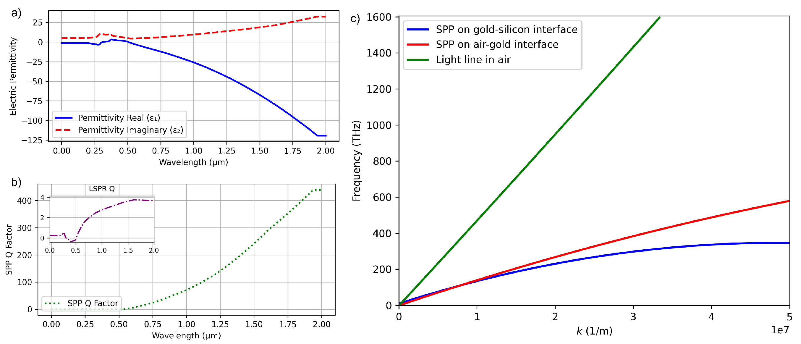
Figure 2.
Surface plot depicting the simulated reflectance of a gold grating as a function of wavelength and incident angle.
Figure 2.
Surface plot depicting the simulated reflectance of a gold grating as a function of wavelength and incident angle.

Figure 3.
(a) Top-view SEM image of bullseye nanostructure arrays; (b) side-view cross-section SEM image; (c) three-dimensional atomic force microscope (AFM) image. (d) Raman spectrum of R6G on with different concentration from M to M from top to bottom; (e) quantitative curve between Raman intensity and R6G concentration; (f) reproducibility at concentration of M at 1310, 1360 and 1505 of the bullseye grating with filling fraction of 0.5 and normalized period of 0.509.
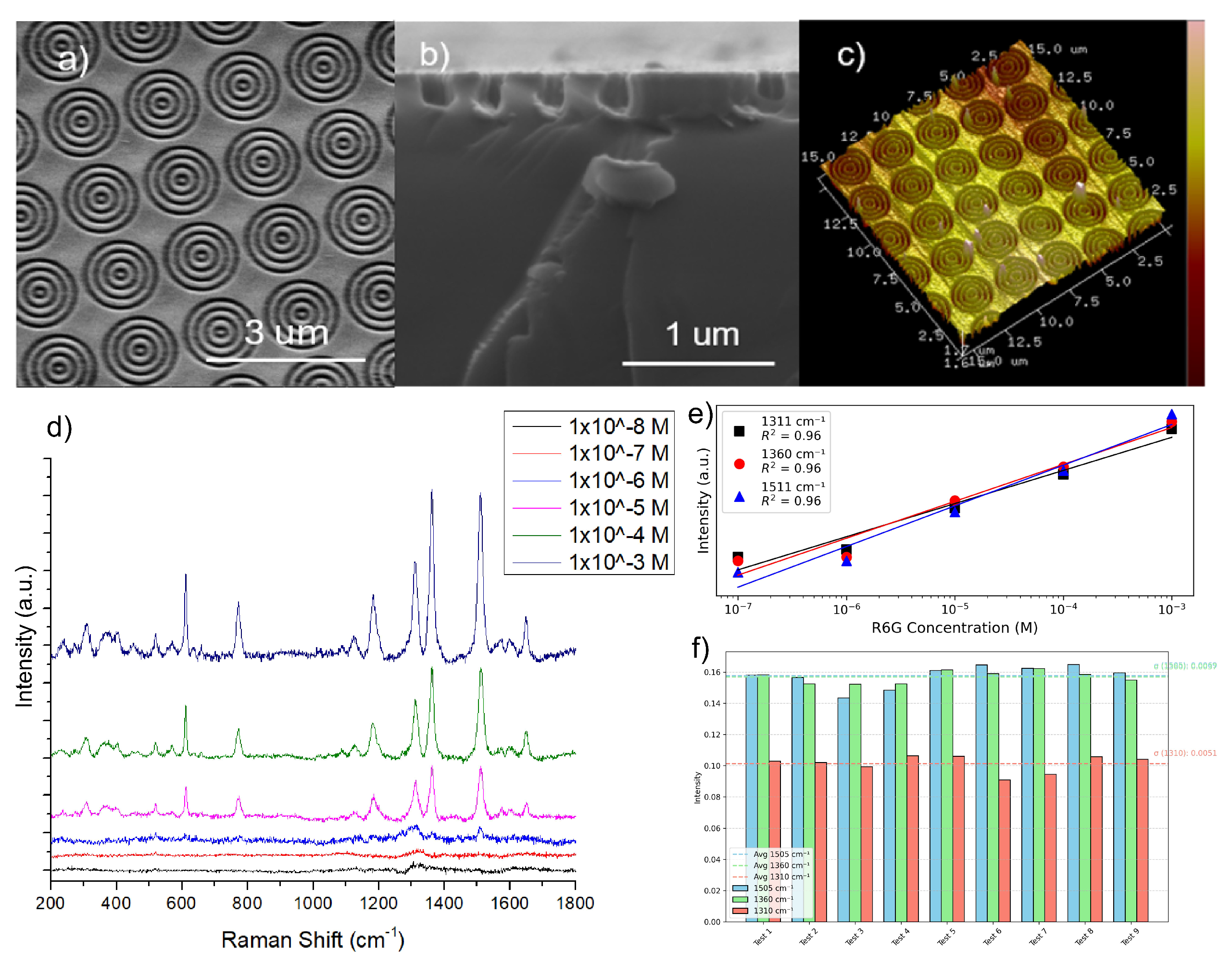
Figure 4.
(a) Calculated intensity of the local electric field versus the normalized period and filling fraction. (b) 3D electric field distributions (in V/m) in the x-z cross-sectional plane and electric field distributions on the y-z cross-sectional plane of the unit cell gold coated bullseye grating with filling fraction of 0.231 and normalized period of 0.331 under TM illumination. (c) Simulated and (d) experimentally calculated enhancement factor versus the grating period and filling fraction, where the simulated are superposed with ; experimental calculations are determined for the Raman bands at 1360 cm−1. (e) shows electric field strength, and (f) displays simulated EF (marked with crosses) and experimental EF (marked with hollow circles) fitted onto the curve.
Disclaimer/Publisher’s Note: The statements, opinions and data contained in all publications are solely those of the individual author(s) and contributor(s) and not of MDPI and/or the editor(s). MDPI and/or the editor(s) disclaim responsibility for any injury to people or property resulting from any ideas, methods, instructions or products referred to in the content. |
© 2025 by the authors. Licensee MDPI, Basel, Switzerland. This article is an open access article distributed under the terms and conditions of the Creative Commons Attribution (CC BY) license (http://creativecommons.org/licenses/by/4.0/).
Copyright: This open access article is published under a Creative Commons CC BY 4.0 license, which permit the free download, distribution, and reuse, provided that the author and preprint are cited in any reuse.


