Submitted:
20 November 2025
Posted:
21 November 2025
You are already at the latest version
Abstract
This study aims to implement universal logic gates using polarity control within a single silicon transistor structure. For this purpose, a reconfigurable transistor based on a p-i-n structure featuring two polarity gates (PGs) and one control gate was proposed, and its electrical characteristics and logic-in-memory (LIM) circuit operations were analyzed via two-dimensional technology computer-aided design simulations. The proposed device could be perfectly reconfigured into p-channel or n-channel modes because virtual doping effects could be induced according to the polarity of the PG voltage. Moreover, based on the positive feedback and latch-up phenomena, a steep subthreshold swing of approximately 1 mV/dec and a high ON/OFF current ratio of the order of 10^10 were achieved. Building on these characteristics, we successfully verified NAND LIM operation in the p-channel mode and NOR LIM operation in the n-channel mode by connecting two of the proposed devices in parallel. The reconfigurable silicon transistor proposed in this study could perform both NAND and NOR LIM operations while sharing the same device structure and can be expected to play a key role in implementing high-density, low-power LIM systems in the future.
Keywords:
polarity gate
; control gate
; universal logic-in-memory gate
1. Introduction
In modern computing, where data-intensive applications such as artificial intelligence and big data analytics are becoming increasingly important, the von Neumann architecture suffers from latency and high power consumption owing to frequent data transfers, resulting in a performance bottleneck [1]. This problem arises from the physical separation of the processor and memory inherent in the von Neumann architecture. Consequently, logic-in-memory (LIM) architectures have been explored [2,3,4]. LIM architectures enable both logic and memory operations within a single physical block, eliminating the need for frequent data movement and thereby improving computational speed and energy efficiency. This approach has garnered considerable attention as a promising strategy for next-generation, low-power, high-efficiency computing applications. Although various devices, such as resistive random-access memory and magnetic random-access memory, have been proposed for implementing LIM architectures, they suffer from high operating voltages and complex control mechanisms. Additionally, static random-access memory (SRAM)-based LIM structures offer the advantage of high-speed operation but are limited in terms of their integration density and leakage current [5,6]. Recently, feedback field-effect transistors (FBFETs) based on a positive-feedback mechanism have garnered attention as promising devices for LIM applications [7,8,9,10]. The positive-feedback mechanism controls the charge carrier injection according to the potential barrier, operating the device through the formation of a positive-feedback loop [11]. This mechanism enables FBFETs to achieve abrupt switching at low operating voltages while exploiting hysteresis characteristics for simultaneous memory operation [12,13,14]. Moreover, as shown in Figure 1(a), the reconfigurable nature of the device—achieved by controlling the polarity of the three gates—enables channel selection according to the majority carrier, making it suitable for LIM applications [15].
In this study, we implemented NAND and NOR gates capable of simultaneous logic and memory operations using a three-gate transistor. The gates located at both ends of the transistor function as polarity gates (PGs) that determine the channel mode according to the polarity of the applied voltage. The centrally located gate serves as a control gate (CG), regulating the injection of charge carriers. The operation of the device is determined by the applied voltage. In p-channel mode, a positive voltage is applied to the drain, whereas in n-channel mode, a negative voltage is applied to the source. Using this operating scheme and configuring the transistor with a resistor in a pull-up and pull-down structure, logic functions, such as NAND and NOR, and memory operations can be simultaneously implemented within a single device.
2. Materials and Methods
The reconfigurable silicon transistor used in this study was based on a p-i-n structure, as illustrated in Figure 1(a). It was fabricated on a p-type silicon substrate (doping concentration of 1015 cm-3) and featured a heavily doped p+ drain (1020 cm-3), a heavily doped n+ source (1020 cm-3), and an intrinsic silicon channel of thickness (TSi) 100 nm. Two PGs and one CG were positioned on the gate oxide above the intrinsic channel. The gate oxide thickness (Tox) was 24 nm. Both the gate length (LG) for all gates and the gap between gates were 2 μm. Two-dimensional (2D) device simulations were performed using the Silvaco technology computer-aided design (TCAD) toolset to analyze the device characteristics. The device structure was generated using Silvaco Athena, and the electrical characteristics were simulated using Silvaco Atlas in mixed mode. The following physical models were employed in the simulations to ensure accuracy—that is, the Fermi-Dirac statistics [16] (Fermi), Lombardi mobility [17], parallel electric field dependence for high-field carrier velocity [18], bandgap narrowing (BGN) [19], concentration-dependent Shockley–Read–Hall recombination, Auger recombination (Auger) [20], and Klaassen mobility [21] models.
3. Results and Discussion
Figure 2 illustrates a schematic of the device structure and energy-band diagrams for p-channel and n-channel operations, depending on the majority of the carriers. The transistor proposed in this study controls the ON/OFF behavior of the device by adjusting the potential barrier height of the charge using three gate voltages. In the OFF state, a potential barrier is formed for both electrons and holes, which inhibits the current flow. Conversely, in the ON state, this barrier is lowered, injecting electrons and holes into the channel region, and the interaction between them creates a positive-feedback loop. Additionally, the device can select the majority carriers as electrons or holes, depending on the voltage of the two PGs, enabling n-channel and p-channel operations, respectively.
When a negative voltage is applied to VPG (VPG < 0), the lower energy band rises, resulting in the same effect as virtual p⁺-type doping of the area. Moreover, a potential barrier is formed for the hole, which inhibits its injection into the channel. As the voltage of the VCG is swept from positive to negative, the hole barrier gradually decreases, and holes are injected from the drain into the channel area, accumulating in the potential well. Consequently, the potential barrier to electrons is lowered, and electrons are injected into the channel, resulting in p-channel behavior, in which holes are the majority carriers.
Conversely, when a positive voltage (VPG > 0) is applied to VPG, the energy band in the region decreases, inducing a virtual n-type doping effect. Consequently, a potential barrier is formed for the electrons, which inhibits their injection. When VCG is swept from negative to positive, electrons are injected into the channel and accumulate in the potential well, decreasing the electron barrier. The hole barrier is then lowered and holes are injected, resulting in n-channel behavior, in which electrons are the majority carriers.
Figure 3(a) and 3(b) show the IDS characteristics of VDS in the n-channel and p-channel operations. Applying −3 V to VPG results in the device being virtually doped as p+- p*- i- p*- n+. The potential barrier formed by the applied voltage prevents the injection of holes and electrons into the channels. In this configuration, sweeping VDS from 0 to 5 V reduces the potential barrier for holes in the drain region. The injected holes accumulate in the potential well, lowering the potential barrier for electrons. This process initiates a positive-feedback loop, leading to an abrupt turn-on and latch-up.
As shown in Figure 3(a), varying VCG from 1 to 4 V results in latch-up voltages of approximately 1.5, 2.5, 3.5, and 4.5 V, respectively. Figure 3 (b) shows a device virtually doped with p+- n*- i- n*- n+ when 3 V is applied to VPG. Sweeping VSD from 0 to −5 V lowers the potential barrier for electrons in the source region, facilitating electron injection into the channel. These injected electrons accumulate in the potential well, thereby reducing the potential barrier for holes. Consequently, a positive-feedback loop is formed, leading to abrupt switching and latch-up behavior. The latch-up voltage increases with VCG and was observed to be approximately −1, −2, −3, and −4 V, respectively.
Figure 3(c) and 3(d) show the IDS characteristic according to VCG for the p-channel and n-channel operations of the transistor, respectively. The two graphs show that the steep switching of the device and clear separation of the ON and OFF states are bistable. Figure 3(c) shows the IDS transfer characteristics as a function of VCG in the p-channel mode with VPG fixed at −3 V. As VCG decreases from 3 to −3 V, the potential barrier in the drain region initially suppresses hole injection, but the barrier is lowered with increasing VCG, injecting holes into the channel region. Consequently, a positive-feedback loop is formed, leading to abrupt switching behavior with a subthreshold swing (SS) of approximately 1 mV/dec and an ON/OFF current ratio of the order of 1010.
Figure 3(d) illustrates that, in n-channel mode, the device turns on more rapidly as VDS increases. This behavior can be attributed to enhanced electron injection, which facilitates internal potential changes and, in turn, promotes more rapid formation of the feedback loop. Under these conditions, the ON/OFF current ratio exceeds 10¹⁰, and the SS is below 1 mV/dec.
Figure 4(a) shows the NAND circuit constructed using two reconfigurable silicon transistors in a parallel configuration and a pull-down resistor. A common voltage of −3 V was applied to the PGs of both transistors to set them to operate in p-channel mode. To receive external inputs, the CG of the left transistor is defined as VIN1, and the VCG of the right transistor is defined as VIN2. Voltage (VDD) is applied to the drain side of the parallel transistor. The operation of the circuit is determined by the positive-feedback mechanism within the transistors.
The AC simulation waveforms verified the NAND LIM operation, as shown in Figure 4(b). When the voltage polarities of VPG and VCG are the same (e.g., VPG < 0 and VCG < 0), positive feedback is activated. If feedback is activated in at least one of the two transistors, the positive voltage VDD applied to the drain side is transferred to the output terminal VOUT, resulting in a positive output signal. This state is defined as logic “1.” Conversely, if the polarities of VPG and VCG are different for both transistors (e.g., VPG < 0 and VCG > 0), the feedback is deactivated. In this case, the VDD voltage is blocked, and the circuit is pulled to the ground state by the pull-down resistor, resulting in an output of 0 V at VOUT. This state is defined as logic “0.” The logical operation of the circuit corresponds to the truth table of the NAND gate. Based on the provided voltage conditions, a negative input (VIN) is defined as logic “0” (−3 V), and a positive input is defined as logic “1” (3 V). A positive output (VOUT) is defined as logic “1,” and an output of 0 V is defined as logic “0.” For input ‘00’ (VIN1 = −3 V, VIN2 = −3 V), the polarities of VPG (VPG < 0) and VCG (VCG < 0) are the same for both transistors, so the positive feedback is ON. Therefore, VDD is transferred to VOUT, resulting in a positive output (logic “1”). For input ‘01’ (VIN1 = −3 V, VIN2 = 3 V), the polarities of VPG (VPG < 0) and VCG (VCG < 0) are the same in the left transistor, so the feedback is ‘ON,’ and VOUT is positive (logic “1”). Similarly, for input ‘10’ (VIN1 = 3 V, VIN2 = −3 V), the polarities of VPG (VPG < 0) and VCG (VCG < 0) are the same in the right transistor, activating the feedback and resulting in a positive output (logic “1”). Finally, for input ‘11’ (VIN1 = 3 V, VIN2 = 3 V), the polarities of VPG (VPG < 0) and VCG (VCG > 0) are different for both transistors, so the feedback is ‘OFF.’ Consequently, VDD is blocked, and VOUT is 0 V (logic “0”).
The NOR circuit was constructed using two reconfigurable silicon transistors and one pull-up resistor, as shown in Figure 5(a). A common voltage of 3 V was applied to the PGs of both transistors to set them to operate in n-channel mode. The VCG of the left transistor is defined as VIN1, and the VCG of the right transistor is defined as VIN2 to receive external inputs. The operation of the circuit is determined by the positive-feedback mechanism within the transistors.
Figure 5(b) shows the AC simulation waveforms, which validate the operation of the NOR LIM. When the voltage polarities of VPG and VCG are the same (e.g., VPG > 0 and VCG > 0), positive feedback is activated. If feedback is activated in at least one of the two transistors, the negative voltage VSS applied to the source side is transferred to the output terminal VOUT, resulting in a negative output signal. This state is defined as logic “0.” Conversely, if the polarities of VPG and VCG are different for both transistors (e.g., VPG > 0 and VCG < 0), the feedback is deactivated. In this case, the VSS voltage is blocked, and the circuit goes to the ground state, resulting in an output of 0 V at VOUT. This state is defined as logic “1.”
Figure 5(b) shows the AC simulation results used to verify the logical operation of the circuit. A negative input (VIN) is defined as logic “0,” and a positive input is defined as logic “1.” A negative output (VOUT) of −0.3 V is defined as logic “0,” and an output of 0 V is defined as logic “1.” The simulation results were consistent with the NOR gate truth table. For input ‘00’ (VIN1 = −3 V, VIN2 = −3 V), the polarities of VPG (VPG > 0) and VCG (VCG < 0) are different for both transistors, so the positive feedback is ‘OFF,’ resulting in VOUT being 0 V (logic “1”). For input 01 (VIN1 = −3 V, VIN2 = 3 V), the polarities of VPG (VPG > 0) and VCG (VCG > 0) are the same in the right transistor, so the feedback is ‘ON’, and VOUT is approximately −0.3 V (logic "0"). Similarly, for input 10 (VIN1 = 3 V, VIN2 = −3 V), the polarities of VPG (VPG > 0) and VCG (VCG > 0) are the same in the left transistor, activating feedback and resulting in VOUT being approximately 0.3 V (logic “0”). Finally, for input ’11’ (VIN1 = 3 V, VIN2 = 3 V), the polarities of VPG (VPG > 0) and VCG (VCG > 0) are the same for both transistors, so the feedback is ‘ON,’ and VOUT is approximately −0.3 V (logic “0”).
4. Conclusions
In this study, we demonstrated a reconfigurable silicon transistor based on a p-i-n structure, aimed at implementing an LIM architecture to overcome the limitations of the von Neumann structure, and verified its superior characteristics using 2D TCAD simulations. The proposed device could be perfectly reconfigured into p-channel and n-channel modes solely by controlling the polarity of the PG voltage. This reconfigurable operation provided hardware-level flexibility, which reduced the circuit complexity and improved the integration density. Moreover, based on the positive feedback and latch-up phenomena, the device achieved a steep SS of approximately 1 mV/dec and a high ON/OFF current ratio of the order of 1010, signifying that a clear switching operation was possible under ultralow power conditions. Building on these characteristics, we successfully implemented a universal logic gate by connecting two identical devices in parallel, demonstrating NAND LIM operation in p-channel mode and NOR LIM operation in n-channel mode within a single-device structure. In conclusion, the proposed device is highly suitable for LIM operations and enables computational and memory functions without requiring data movement. It provides a universal gate that is hardware-reconfigurable and possesses ultralow-power switching characteristics. The findings of this study are expected to contribute to the core device technology for future high-density, low-power next-generation computing systems.
Author Contributions
Conceptualization, S. H.; Methodology, S. H., N. H., and Y. Y.; Validation, S. H., N. H., and Y. Y.; Formal Analysis, S. H., N. H., and Y. Y.; Investigation, S. H., N. H., and Y. Y.; Writing—Original Draft, S. H. and N. H.; Writing—Review and Editing, D. L.; Visualization, S. H., N. H., Y. Y., and D. L.; Supervision, D. L.; Project Administration, D. L. All authors have read and agreed to the published version of this manuscript.
Funding
This work was supported by the Korea Collaborative & High-Tech Initiative for Prospective Semiconductor Research (1415187357, RS-2023-00230336, 23004-15TC) funded by the Ministry of Trade, Industry, and Energy (MOTIE, Korea) and a National Research Foundation of Korea (NRF) grant funded by the Korean Government (MSIT) (Grant No. RS-2023-00217791).
Data Availability Statement
Data are contained within the article
Conflicts of Interest
The authors declare no conflicts of interest.
Abbreviations
The following abbreviations are used in this manuscript:
| BGN | Bandgap narrowing |
| CG | Control gate |
| FBFET | Feedback field-effect transistor |
| LIM | Logic-in-memory |
| PG | Polarity gate |
| SS | Subthreshold swing |
| TCAD | Technology computer-aided design |
References
- Kudithipudi, D.; Schuman, C.; Vineyard, C.M.; Pandit, T.; Merkel, C.; Kubendran, R.; Aimone, J.B.; Orchard, G.; Mayr, C.; Benosman, R.; et al. Neuromorphic Computing at Scale. Nature 2025, 637, 801–812. [Google Scholar] [CrossRef] [PubMed]
- Ghose, S.; Boroumand, A.; Kim, J.S.; Gómez-Luna, J.; Mutlu, O. Processing-in-Memory: A Workload-Driven Perspective. IBM J. Res. Dev. 2019, 63, 3–1. [Google Scholar] [CrossRef]
- Asifuzzaman, K.; Miniskar, N.R.; Young, A.R.; Liu, F.; Vetter, J.S. A Survey on Processing-in-Memory Techniques: Advances and Challenges. Memories - Mater. Devices, Circuits Syst. 2023, 4, 100022. [Google Scholar] [CrossRef]
- Wang, C.; Shi, G.; Qiao, F.; Lin, R.; Wu, S.; Hu, Z. Research Progress in Architecture and Application of RRAM with Computing-in-Memory. Nanoscale Adv. 2023, 5, 1559–1573. [Google Scholar] [CrossRef] [PubMed]
- Zahoor, F.; Hussin, F.A.; Isyaku, U.B.; Gupta, S.; Khanday, F.A.; Chattopadhyay, A.; Abbas, H. Resistive Random Access Memory: Introduction to Device Mechanism, Materials and Application to Neuromorphic Computing. Discov. nano 2023, 18, 36. [Google Scholar] [CrossRef] [PubMed]
- Chen, J.; Zhao, W.; Wang, Y.; Shu, Y.; Jiang, W.; Ha, Y. A Reliable 8T SRAM for High-Speed Searching and Logic-in-Memory Operations. IEEE Trans. Very Large Scale Integr. Syst. 2022, 30, 769–780. [Google Scholar] [CrossRef]
- Lee, C.; Shin, C. Study on Various Device Structures for Steep-Switching Silicon-on-Insulator Feedback Field-Effect Transistors. IEEE Trans. Electron Devices 2020, 67, 1852–1858. [Google Scholar] [CrossRef]
- Katta, S.S.; Kumari, T.; Srinivas, P.S.T. .; Tiwari, P.K. Logic-in-Memory Application of Silicon Nanotube-Based FBFET with Core-Source Architecture. Microelectronics J. 2024, 146, 106133. [Google Scholar] [CrossRef]
- Lim, E.; Son, J.; Cho, K.; Kim, S. Logic and Memory Characteristics of an Inverter Comprising a Feedback FET and a MOSFET. Semicond. Sci. Technol. 2022, 37, 65025. [Google Scholar] [CrossRef]
- Lim, D.; Cho, K.; Kim, S. Single Silicon Neuron Device Enabling Neuronal Oscillation and Stochastic Dynamics. IEEE Electron Device Lett. 2021, 42, 649–652. [Google Scholar] [CrossRef]
- Lee, C.; Sung, J.; Shin, C. Understanding of Feedback Field-Effect Transistor and Its Applications. Appl. Sci. 3070. [CrossRef]
- Kim, Y.; Cho, J.; Lim, D.; Woo, S.; Cho, K.; Kim, S. Switchable-Memory Operation of Silicon Nanowire Transistor. Adv. Electron. Mater. 2018, 1800429, 1–7. [Google Scholar] [CrossRef]
- Lim, D.; Cho, K.; Kim, S. Reconfigurable Logic-in-Memory Using Silicon Transistors. Adv. Mater. Technol. 2022, 7, 2101504. [Google Scholar] [CrossRef]
- Lim, D.; Son, J.; Cho, K.; Kim, S. Quasi-nonvolatile Silicon Memory Device. Adv. Mater. Technol. 2020, 5, 2000915. [Google Scholar] [CrossRef]
- Lim, D.; Kim, S. Polarity Control of Carrier Injection for Nanowire Feedback Field-Effect Transistors. Nano Res. 2019, 12, 2509–2514. [Google Scholar] [CrossRef]
- Physics and Properties of Semiconductors—A Review. In Physics of Semiconductor Devices; 2006; pp. 5–75 ISBN 9780470068328.
- Lombardi, C.; Manzini, S.; Saporito, A.; Vanzi, M. A Physically Based Mobility Model for Numerical Simulation of Nonplanar Devices. IEEE Trans. Comput. Des. Integr. Circuits Syst. 1988, 7, 1164–1171. [Google Scholar] [CrossRef]
- Canali, C.; Majni, G.; Minder, R.; Ottaviani, G. Electron Drift Velocity in Silicon. Phys. Rev. B 1975, 12, 2265–2284. [Google Scholar] [CrossRef]
- Slotboom, J.W.; de Graaff, H.C. Measurements of Bandgap Narrowing in Si Bipolar Transistors. Solid. State. Electron. 1976, 19, 857–862. [Google Scholar] [CrossRef]
- Dziewior, J.; Schmid, W. Auger Coefficients for Highly Doped and Highly Excited Silicon. Appl. Phys. Lett. 1977, 31, 346–348. [Google Scholar] [CrossRef]
- Klaassen, D.B.M. A Unified Mobility Model for Device Simulation—Part I: Model Equations and Concentration Dependence. Solid. State. Electron. 1992, 35, 953–959. [Google Scholar] [CrossRef]
Figure 1.
(a) Schematic cross-section and circuit symbols of the proposed reconfigurable silicon transistor. (b) Key structural and electrical parameters used in the TCAD simulation, including the gate length, oxide thickness, and doping concentrations.
Figure 1.
(a) Schematic cross-section and circuit symbols of the proposed reconfigurable silicon transistor. (b) Key structural and electrical parameters used in the TCAD simulation, including the gate length, oxide thickness, and doping concentrations.
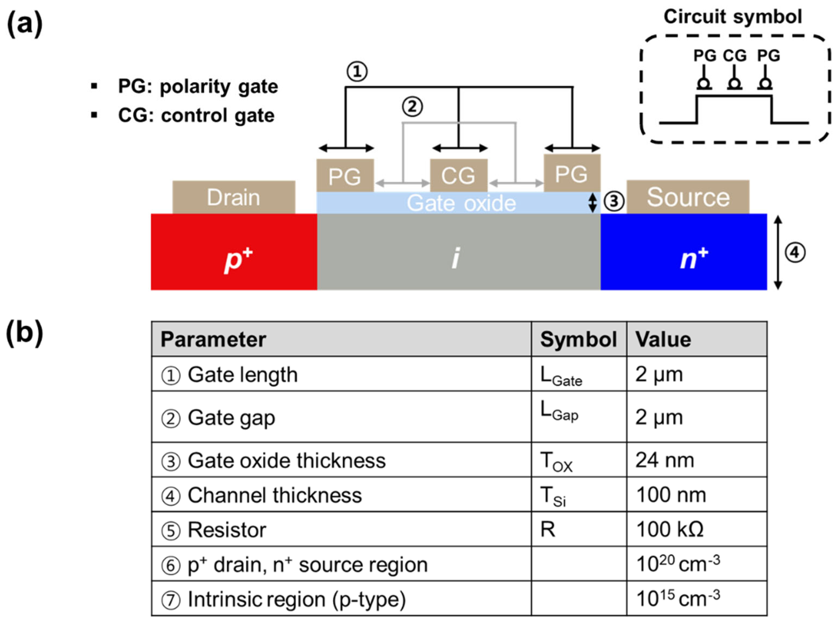
Figure 2.
Operating mechanism of the reconfigurable transistor based on the voltage applied to VPG, with device structure and energy-band diagrams for the (a) p-channel and (b) n-channel operations.
Figure 2.
Operating mechanism of the reconfigurable transistor based on the voltage applied to VPG, with device structure and energy-band diagrams for the (a) p-channel and (b) n-channel operations.
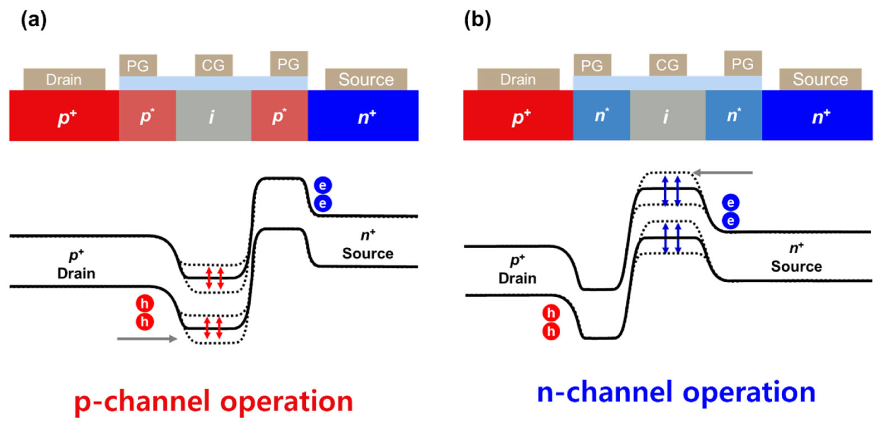
Figure 3.
Electrical characteristics of the transistor: output characteristics for the (a) p-channel and (b) n-channel under different control gate voltages, and transfer characteristics for the (c) p-channel and (d) n-channel as a function of the drain–source voltage.
Figure 3.
Electrical characteristics of the transistor: output characteristics for the (a) p-channel and (b) n-channel under different control gate voltages, and transfer characteristics for the (c) p-channel and (d) n-channel as a function of the drain–source voltage.
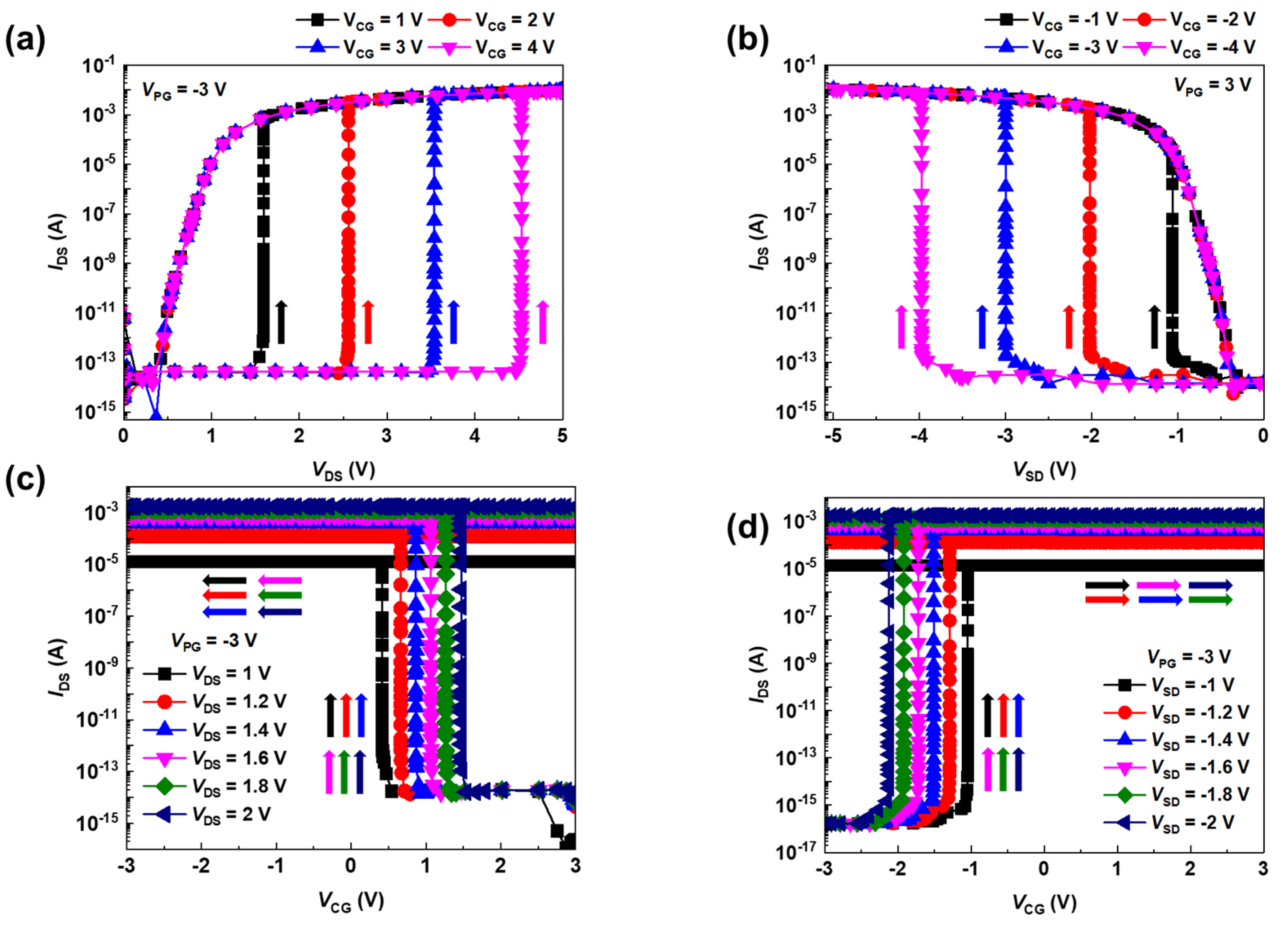
Figure 4.
(a) Logic circuit diagram composed of two reconfigurable silicon transistors and a pull-down resistor. (b) AC simulation waveforms verifying the NAND LIM gate operation, showing the output signal VOUT in response to the input signals VIN1 and VIN2.
Figure 4.
(a) Logic circuit diagram composed of two reconfigurable silicon transistors and a pull-down resistor. (b) AC simulation waveforms verifying the NAND LIM gate operation, showing the output signal VOUT in response to the input signals VIN1 and VIN2.
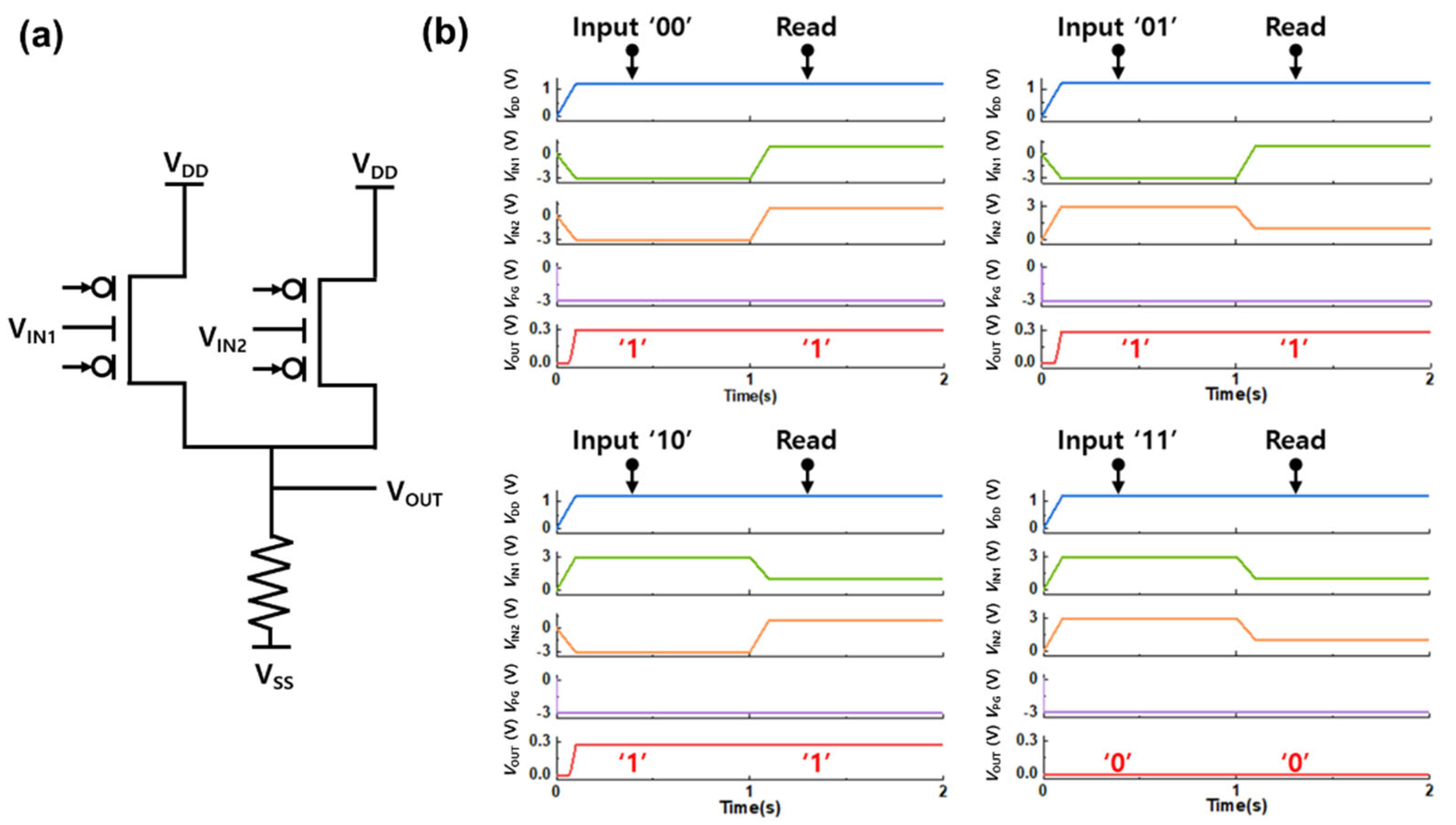
Figure 5.
(a) Logic circuit diagram composed of two reconfigurable silicon transistors and a pull-up resistor. (b) AC simulation waveforms verifying the NOR LIM operation, showing the output signal VOUT in response to the input signals VIN1 and VIN2.
Figure 5.
(a) Logic circuit diagram composed of two reconfigurable silicon transistors and a pull-up resistor. (b) AC simulation waveforms verifying the NOR LIM operation, showing the output signal VOUT in response to the input signals VIN1 and VIN2.

Disclaimer/Publisher’s Note: The statements, opinions and data contained in all publications are solely those of the individual author(s) and contributor(s) and not of MDPI and/or the editor(s). MDPI and/or the editor(s) disclaim responsibility for any injury to people or property resulting from any ideas, methods, instructions or products referred to in the content. |
© 2025 by the authors. Licensee MDPI, Basel, Switzerland. This article is an open access article distributed under the terms and conditions of the Creative Commons Attribution (CC BY) license (http://creativecommons.org/licenses/by/4.0/).
Copyright: This open access article is published under a Creative Commons CC BY 4.0 license, which permit the free download, distribution, and reuse, provided that the author and preprint are cited in any reuse.


