
Submitted:
12 November 2025
Posted:
13 November 2025
You are already at the latest version
Abstract
Post-quantum cryptography (PQC) is rapidly being standardized, with key primitives such as Key Encapsulation Mechanisms (KEMs) and Digital Signature Algorithms (DSAs) moving into practical applications. While initial research focused on pure software and hardware implementations, the focus is shifting toward flexible, high-efficiency solutions suitable for widespread deployment. A system-on-chip is a viable option with the ability to coordinate between hardware and software flexibly. However, the main drawback of this system is the time needed to exchange data during computation. Currently, most SoCs are implemented on FPGAs, and there is a lack of SoCs realized on ASICs. This paper introduces a complete RISC-V SoC design on an ASIC for Module Lattice-KEM. Our system features a RISC-V processor tightly integrated with a high-efficiency Number Theoretic Transform (NTT) accelerator. This accelerator is leveraging custom instructions to speed up cryptographic operations. Our research has achieved the following results: 1) The accelerator provides a speedup of up to 14.51 × for NTT and 16.75 × for inverse NTT operations compared to other RISC-V platforms; 2) This leads to end-to-end performance improvements for ML-KEM of up to 56.5% for security level I, 50.9% for level III, and 45.4% for level V; 3) The ASIC design is fabricated using a 180nm CMOS process at a maximum operating frequency of 118 MHz with an area overhead of 11.18%, with a minimum power consumption of 5.913 μW at 10 kHz and 0.9 V of supply voltage.
Keywords:
post-quantum cryptography
; PQC
; NIST
; PKE
; KEM
; RISC-V
; FPGA
; signatures schemes
1. Introduction
As the volume of data shared across devices like computers, smartphones, and IoT gadgets explodes, so does the risk of data leakage. Communication channels are vulnerable to eavesdropping, making robust security crucial. Traditional data protection often relies on symmetric encryption, where the sender and receiver use the same secret key. However, this method has a critical weakness: if that single key is compromised, the entire communication is at risk. To solve this, the Key Encapsulation Mechanism (KEM) was developed to securely exchange these shared keys.
The rise of quantum computing presents a significant threat to these traditional KEMs. Quantum computers could break them in polynomial time. In response, the National Institute of Standards and Technology (NIST) initiated a program to standardize new cryptographic algorithms that are secure against quantum attacks. This field is known as post-quantum cryptography (PQC).
The official PQC standards include CRYSTALS-Kyber (FIPS 203) [1] and Hamming Quasi-Cyclic for KEM. Digital signatures consist of CRYSTALS-Dilithium (FIPS 204) [2], FALCON [3], and SPHINCS+ (FIPS 205) [4]. The FIPS 203 is the first standardized KEM, making it a primary focus for research and optimization. ML-KEM’s security is based on the complexity of the Shortest Vector Problem in high-dimensional lattices. A major computational challenge for ML-KEM is the reliance on polynomial multiplication, which dominates the algorithm’s runtime.
Several studies have focused on accelerating polynomial multiplication for ML-KEM on various hardware platforms[5,6,7,8]. Some have explored pure hardware solutions, while others have targeted System-on-Chip (SoC) platforms[9,10,11,12], which is a growing trend for PQC implementation[13]. In an SoC, hardware accelerators can be loosely connected to system buses or tightly integrated into the CPU. The advantage of being loosely coupled is that it is simple and easy to implement, but in return, loading and storing data from/to memory is a barrier to accelerating computation. Tightly-coupled designs offer superior acceleration efficiency. Currently, there are very few practical on-chip implementations to evaluate system-level performance, creating a significant research gap.
We designed and fabricated an SoC that directly addresses this gap. Our design features an accelerator for forward/inverse Number Theoretic Transform (NTT/INTT), central to ML-KEM’s polynomial multiplication. The accelerator uses a dual butterfly unit (BU) architecture and is tightly integrated into a 64-bit RISC-V CPU via the Rocket Custom Coprocessor (RoCC) interface. To our knowledge, this is the first physical chip implementation of an SoC for ML-KEM.
Our results demonstrate significant performance gains:
- Performance: The accelerator provides a speedup of up to 14.51 × for NTT and 16.75 × for inverse NTT operations compared to other RISC-V platforms.
- Efficiency: We achieved speedup efficiencies of 56.5%, 50.9%, and 45.4% for security levels I, III, and V, respectively. This performance comes with a minimal area overhead of 11.18%.
- ASIC Fabrication: The complete chip was fabricated using 180 nm CMOS technology, with a total area of 297 k gate equivalents (GE), consuming a minimum of at an operation frequency of 10 kHz and a VDD of 0.9 V. The SoC achieved a maximum frequency of 118 MHz at a supply voltage of 2.0 V.
2. Background
ML-KEM is a module lattice-based KEM built upon public-key encryption principles. The key establishment process is illustrated in Figure 1. The sender generates a pair of encryption () and decryption keys (), then sends the to the receiver over an unsecured channel. The receiver then uses to generate a shared secret key K and encapsulates it by encrypting a message m to produce a ciphertext c. This ciphertext is sent back to the sender over a public channel. Upon receiving c, the sender uses the to recover the message , which is then used with to derive the shared secret key . This shared key is subsequently used as the secret key for data transmission using symmetric encryption.
The functions of ML-KEM are based on the multiplication of polynomials in the ring , with polynomial of the form , and integer coefficients in for all i, with and . The operations in the ring include addition, subtraction, and multiplication performed modulo . The NTT is employed to accelerate polynomial multiplication. Given polynomials f and g, their representation in the NTT domain is denoted as and . For the ML-KEM, let be the product of two polynomials on the NTT domain, then is calculated by multiplication as described in Eq. 1.
where the indices and represent, respectively, the even and odd coefficients of the polynomials in the multiplication, and is an integer represented by bit-reversing the unsigned value . Finally, the product of 2 polynomials on the normal domain is achieved by .
However, polynomial multiplication still remains a computational bottleneck in the execution of ML-KEM. The overall efficiency still depends on how effectively the NTT is implemented. This challenge becomes more significant at higher security levels, where the number of polynomials involved in matrix-vector multiplications increases. The two most commonly adopted structures for BU are Cooley–Tukey (CT) [14] and Gentleman–Sande (GS) [15], which differ in the ordering of transformation outputs.
Our design adopts CT for the forward NTT, while GS is used for the inverse NTT (INTT) to eliminate the need for additional pre-processing and post-processing. Our target is an embedded system for achieving a balance between execution flexibility and computational speed. RISC-V offers an ideal solution in such contexts by combining the performance benefits of hardware acceleration with the adaptability of software control. RISC-V is an open instruction set architecture designed with modularity, allowing developers to tailor processor architectures to specific application requirements.
This modular approach makes RISC-V highly versatile and suitable for various applications, from lightweight IoT devices to high-performance computing systems.
As an open and modular instruction set architecture, RISC-V enables us to customize processor designs to meet specific application requirements. Integrating a hardware accelerator directly with the CPU can substantially enhance system performance while preserving software flexibility. This integration method helps solve the large latency problem caused by data exchange on SoCs. Custom instructions facilitate efficient control of the accelerator, enabling tight hardware-software integration and improved overall system efficiency.
3. Proposed Architecture
3.1. Rocket RISC-V System-on-Chip
The proposed SoC architecture is illustrated in Figure 2. The system is built on a Rocket Core configured with the RV64IMAC variant, featuring a 1-kB data cache, 4-kB of on-chip RAM, and an external memory interface supporting up to 256 MB. The NTT accelerator is tightly coupled to the CPU via the RoCC interface [16]. This accelerator functions as a co-processor, receiving commands from the CPU and accessing data directly to the memory through the cache. Custom instructions are defined to transmit control and addresses to the accelerator. The accelerator loads the required data at the provided input address, then performs NTT or INTT transformations based on the control information. Finally, the output result is stored directly at the output address. The basic peripheries are connected to the system via the peripheral bus. Peripherals include a UART for printing results, an SPI for loading firmware from an SD card, and a JTAG for system debugging.
Figure 3 illustrates the interface between the CPU and the accelerator. The CMD and RESP lines correspond to the command and response of the CPU with the accelerator. The and signals are used for communication control purposes. Data transfer is carried out via MEM_REQ and MEM_RESP. This tightly coupled interaction enables efficient, low-latency control and data transfer between the CPU and the accelerator.
The custom instruction architecture adheres to the standard RISC-V instruction format. It includes the fields , and . The specifies the custom group from 0 to 3. The , and fields correspond to the destination and source registers, respectively. The accelerator uses the to differentiate between instructions within the same group. We define two custom instructions under the group () specifically for NTT and INTT operations in ML-KEM. The structure of these custom instructions is illustrated in Figure 4.
When a RoCC instruction is fetched and decoded, the presence of the routes it to the accelerator via the RoCC command router. The accelerator interprets the remaining instruction fields to determine the appropriate control signals and begins processing accordingly. The first custom instruction, identified by , loads the source and destination addresses into the accelerator. The second custom instruction with provides the data length and specifies the operation mode, where indicates an NTT operation and indicates an INTT operation. The also signals that all necessary parameters have been received and the accelerator can begin execution. The result is automatically stored to the specified address upon completion. The CPU can then read the result directly from the declared memory region.
Figure 5 illustrates the operation of the accelerator after receiving instructions from the CPU with . The accelerator sends data request instructions to the source address in memory via . The system then returns the requested data. This data is temporarily stored in the FIFO. After sufficient data is in the FIFO, it is sent to the BUs and forward- or inverse-transformed as requested. This process is pipelined until the final result is written back to the FIFO. At that time, the accelerator sends a write request to the destination address via , along with the result retrieved from the FIFO. After the last data in the FIFO is entirely written, the accelerator reports that the execution is complete and returns to the IDLE state.
3.2. NTT accelerator architecture
As shown in Figure 6, the proposed NTT accelerator architecture comprises a computational element that consists of two parallel execution BUs. Modular reduction is performed using the Barrett method [17]. To save the area, the accelerator implements NTT using an iterative procedure. The input polynomial is stored in a simple FIFO of size 64 ×32. Thanks to the feedback shift register-based reordering unit (RU) architecture, the reordering process does not incur additional delays through each stage as in typical MDC architectures.
The accelerator is built on a 64-bit system, so 16 bits are used for each polynomial coefficient, processing four coefficients on a single data call. The outputs of the RU are concatenated into 64-bit blocks and written into the FIFO. The entire process, from loading the input to executing and storing the results, is controlled by the Control Unit. This architecture makes the memory size for temporary results storage minimal without causing read-after-write (RAW) conflicts. Several previous studies required more than the memory needed for storing polynomials [18,19,20]. This architecture supports pipelined execution without any additional memory resources. With this parallelism, each NTT/INTT operation requires 448 clock cycles (CCs).
A finite state machine manages control and synchronization between the accelerator and the RoCC interface, allowing the accelerator to operate independently of the CPU. This setup enables efficient NTT/INTT execution via custom instructions, speeding up the overall algorithm.
4. Implementation Results and Discussion
The proposed SoC was implemented using 180 nm CMOS technology. Figure 7 shows the chip micrograph, with a die area of , corresponding to approximately 297 kGE. The chip reaches a maximum operating frequency of 118 MHz, and a minimum power consumption of at 10kHz and VDD = 0.9 V.
The proposed design incurs a modest area overhead of 11.18% due to integrating the NTT accelerator, yet it delivers a significant performance boost. The efficiency of the accelerator is attributed to its compact architecture, which outperforms previous designs in both area and speed. It features two parallel BUs and a simple FIFO, optimizing area and performance. The streamlined architecture and control logic enable seamless SoC integration with two custom instructions. This simplicity drives the speed-up efficiency in NTT/INTT execution across various RISC-V platforms, as shown in Table 1.
The results demonstrate that tightly coupled acceleration is substantially more efficient than loosely coupled approaches. In typical RISC-V platforms, the main bottleneck in NTT/INTT acceleration lies in memory access latency. Our design overcomes this limitation by directly interfacing with the data cache, significantly reducing memory access time. As a result, the proposed architecture achieves notable speedups of up to for NTT and for INTT compared to other accelerators on different RISC-V platforms.
The bar graph in Figure 8 illustrates the speedup efficiency achieved over the baseline C implementation. By offloading the NTT/INTT computations to the hardware accelerator, overall execution time is significantly reduced. The graph presents the number of CCs required for the Keygen, Encaps, and Decaps processes across different security levels I, III, and V, corresponding to . This improvement in NTT/INTT overhead contributes to an overall system speedup from 37% to 56.5% relative to the baseline.
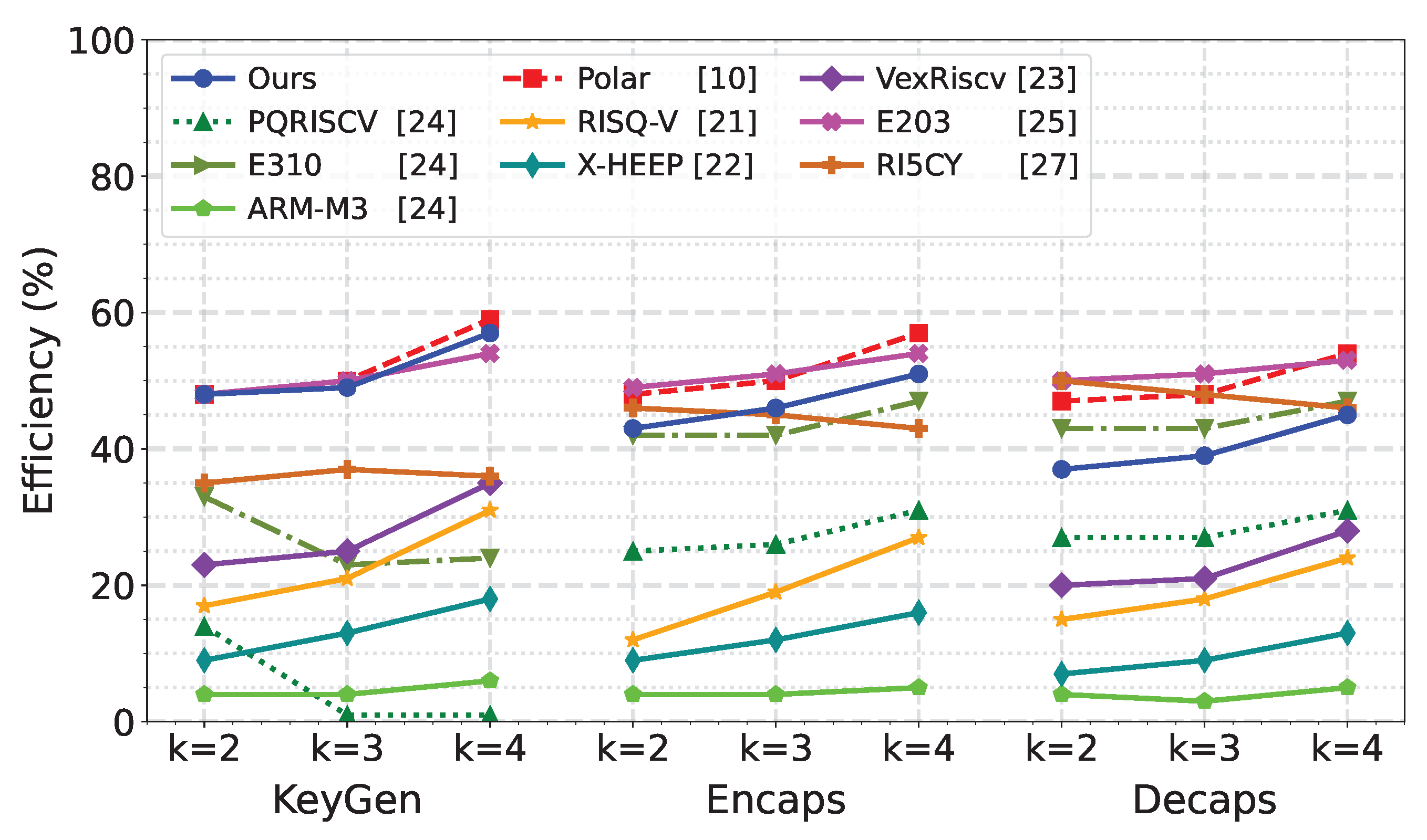
Figure 9 presents the speedup efficiency of the complete ML-KEM algorithm implementation. Given that different RISC-V platforms vary in architecture and baseline performance, the comparison is made regarding relative speedup efficiency. The performance improvement of each implementation relative to its own C reference. This provides a fair basis for evaluating the impact of the accelerator across heterogeneous CPU types. The evaluation method used to compute acceleration efficiency is detailed in Eq. 2.
As shown in Table 1, our proposed design outperforms those in [21], [22], and [23], which achieving efficiency gains between 7% and 35%. While these prior works enhance performance through custom arithmetic instructions, their overall acceleration efficiency remains limited. This limitation stems from the simplicity of the instructions, which require numerous invocations to complete the full algorithm. As a result, the reduction in total execution time is modest compared to our tightly coupled and more integrated acceleration approach.
Several designs implement various acceleration techniques beyond NTT, such as hash function acceleration and sampling, achieving efficiency improvements ranging from 42% to 59%. While our focus is solely on accelerating NTT/INTT, our design still achieves a significant efficiency gain of 37% to 56.5%, comparable to more complex architectures like those in [10,24,25], and [26].
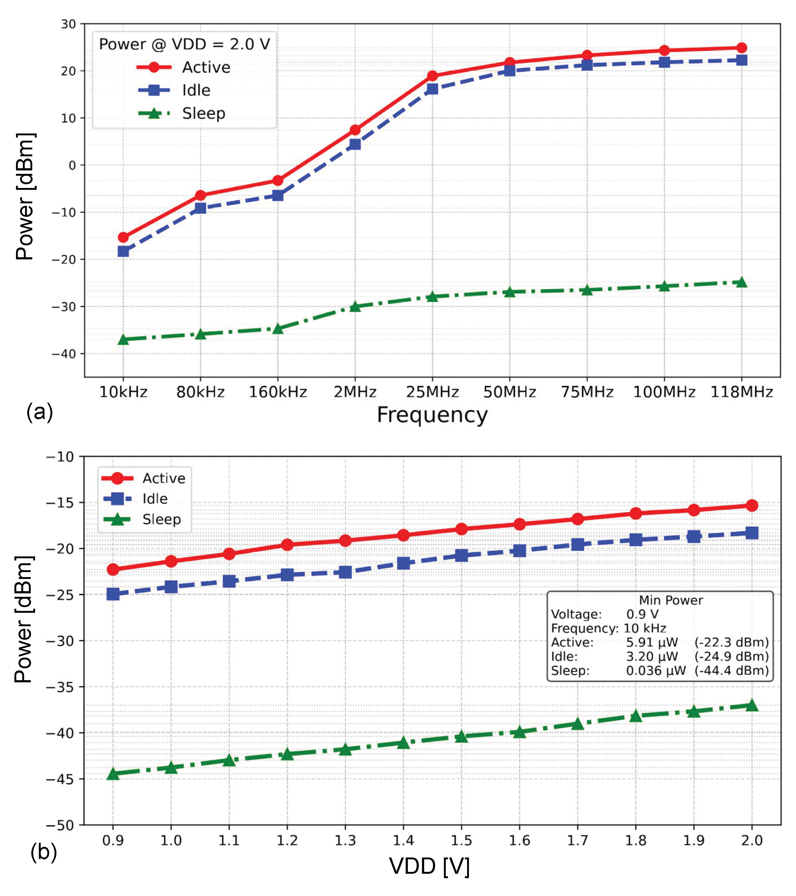
Figure 10 illustrates the power consumption of the SoC at various frequencies and VDD voltages. Figure 10(a) shows the power consumption of the chip at VDD = 2.0 V, in the operating frequency range from 10 kHz to 118 MHz. The power is measured in three states: Active power, when the SoC executes the algorithm; Idle power, the state when the chip resets; and Sleep power, which represents leakage power. We can see that the system consumes at 118 MHz. We can also observe that the leakage power is minimal across all frequency ranges, with a maximum value of approximately . Figure 10(b) shows the power consumption of the system at a 10 kHz frequency, spanning a voltage range from 0.9 V to 2.0 V. The results show that the minimum power consumption of the SoC achieved is , which can be applied to low-power systems.
The wide operating frequency and voltage range make this SoC applicable to a wide range of applications, which opens up a promising future for this efficient design approach as we continue to optimize other system processes.

Table 1.
The NTT/INTT latency (in clock cycles) compared to other works.
| Works | Platform | NTT | INTT | Area Overhead |
||
|---|---|---|---|---|---|---|
| CCs | Latency | CCs | Latency | |||
| Ours | Rocket | 1,514 | 1× | 1,413 | 1× | 11.18% |
| [27] | RI5CY | 2,577 | ↑ 1.70× | 3,851 | ↑ 2.72× | 16% |
| [24] | M3 | 8,026 | ↑ 5.30× | 8,594 | ↑ 6.08× | - |
| E310 | 15,888 | ↑ 10.49× | 15,719 | ↑ 11.12× | - | |
| PQRISCV | 21,975 | ↑ 14.51× | 23,666 | ↑ 16.75× | - | |
| [21] | RISQ-V | 1,935 | ↑ 1.28× | 1,930 | ↑ 1.37× | 60% |
| [28] | Rocket | 4,156 | ↑ 2.75× | 4,172 | ↑ 2.95× | 12.93% |
| [22] | X-HEEP | 1,531 | ↑ 1.01× | 1,531 | ↑ 1.08× | 32.64% |
| [23] | Vex-Riscv | 6,868 | ↑ 4.54× | 6,367 | ↑ 4.51× | 6% |
| [29] | SiFive U74 | 8,845 | ↑ 5.84× | 10,262 | ↑ 7.26× | - |
| 5,700 | ↑ 3.76× | 5,618 | ↑ 3.98× | - | ||
| [25] | E203 | 4,302 | ↑ 2.84× | 3,426 | ↑ 2.42× | 4.3% |
Figure 10.
SoC power consumption (a) at VDD = 2.0 V in the operating frequency range from 10 kHz to 118 MHz and (b) SoC power consumption at 10 kHz in the voltage range from 0.9 V to 2.0 V.
Figure 10.
SoC power consumption (a) at VDD = 2.0 V in the operating frequency range from 10 kHz to 118 MHz and (b) SoC power consumption at 10 kHz in the voltage range from 0.9 V to 2.0 V.
5. Conclusion
Our research presents a RISC-V SoC featuring an integrated NTT accelerator controlled via custom instructions. The SoC consumes a minimum of of power consumption at a 0.9 V supply voltage and 10 kHz frequency in 180 nm CMOS technology. The chip also achieved a maximum operation frequency of 118 MHz at VDD = 2.0 V.
Our SoC architecture outperforms the baseline C implementation by 56.5% at security level I, 50.9% at level III, and 45.4% at level V. This efficiency level is superior to other similar RISC-V platforms. It demonstrates a key insight: a tightly integrated coprocessor is a highly effective way to accelerate complex computational algorithms dramatically.
6. Acknowledgement
The VLSI chip in this paper was fabricated in the chip fabrication program of VLSI Design and Education Center (VDEC), the University of Tokyo, with the collaboration of Rohm Corporation and Toppan Printing Corporation.
This research was supported by JST NEXUS, Japan, under grant number JPMJNX25D4.
References
- National Institute of Standards and Technology. Module-Lattice-Based KeyEncapsulation Mechanism Standard, Aug. 2024.
- National Institute of Standards and Technology. Module-Lattice-Based Digital Signature Standard, Aug. 2024.
- P. -A. Fouque, J. Hoffstein, P. Kirchner, V. Lyubashevsky, T. Pornin, T. Prest, T. Ricosset, G. Seiler, W. Whyte, and Z. Zhang. Falcon: Fast-Fourier Lattice-Based Compact Signatures Over NTRU (v1.2). NIST PQC Round Oct. 2020, pp. 1–67.
- J.-P Aumasson, D.-J. Bernstein, W. Beullens, C. Dobraunig, M. Eichlseder, S. Fluhrer, S.-L. Gazdag, A. Hülsing, P. Kampanakis, S. Kölbl, T. Lange, M. M. Lauridsen, F. Mendel, R. Niederhagen, C. Rechberger, J. Rijneveld, P. Schwabe, and B. Westerbaan. SPHINCS+—Submission To the 3rd Round of the NIST Post-quantum Project, v3.1. NIST PQC Round 2022, pp. 1–63.
- T.-H. Nguyen, D.-T. Dam, P.-P. Duong, K.-D.-N. Binh, C.-K. Pham, and T.-T. Hoang. Efficient Hardware Implementation of the Lightweight CRYSTALS-Kyber. IEEE Trans. on Circ. and Syst. I: Regular Papers 2025, 72, 610–622. [CrossRef]
- Y. Cui, J. Chen, Z. Ni, Z. Zhang, C. Wang, and W. Liu. Instruction-Based High-Performance Hardware Controller of CRYSTALS-Kyber With Balanced Resource Utilization. IEEE Trans. on Circ. and Syst. I: Regular Papers 2025, 72, 2394–2407. [CrossRef]
- H. Kim, H. Jung, A. Satriawan, and H. Lee. A Configurable ML-KEM/Kyber Key-Encapsulation Hardware Accelerator Architecture. IEEE Trans. on Circ. and Syst. II: Express Briefs 2024, 71, 4678–4682. [CrossRef]
- T.-H. Nguyen, T.-K. Dang, D.-T. Dam, K.-D. Nguyen, P.-P. Duong, C.-K. Pham, and T.-T. Hoang. An Area-Time Efficient Hardware Architecture for ML-KEM Post-Quantum Cryptography Standard. IEEE Access 2025, 13, 103834–103847. [CrossRef]
- C. Gewehr, L. Luza, and F.-G Moraes. Hardware Acceleration of Crystals-Kyber in Low-Complexity Embedded Systems With RISC-V Instruction Set Extensions. IEEE Access 2024, 12, 94477–94495. [CrossRef]
- T. Wang, C. Zhang, X. Zhang, D. Gu, and P. Cao. Optimized Hardware-Software Co-Design for Kyber and Dilithium on RISC-V SoC FPGA. IACR Trans. on Crypt. Hard. and Embedded Syst. Jul. 2024, 2024, 99–135. [CrossRef]
- Z. Ye, R. Song, H. Zhang, D. Chen, R.-C.-C. Cheung, and K. Huang. A Highly-efficient Lattice-based Post-Quantum Cryptography Processor for IoT Applications. IACR Trans. on Crypt. Hard. and Embedded Syst. Mar. 2024, 2024, 130–153. [CrossRef]
- D.-T. Dam, T.-H. Nguyen, K.-D.-N. Binh, T.-T. Hoang, and C.-K. Pham. RISC-V SoC with NTT-Blackbox for CRYSTALS-Kyber Post-Quantum Cryptography. In Proceedings of the 2024 9th Int. Conf. on Inte. Circ., Design, and Verification (ICDV), Jun. 2024, pp. 49–54.
- D.-T. Dam, T.-H. Tran, V.-P. Hoang, C.-K. Pham, and T.-T. Hoang. A Survey of Post-Quantum Cryptography: Start of a New Race. Cryptography 2023, 7. [CrossRef]
- J. W. Cooley and J. W. Tukey. An Algorithm for the Machine Calculation of Complex Fourier Series. Math. of Computation Apr. 1965, 19, 297–301. [CrossRef]
- W. M. Gentleman and G. Sande. Fast Fourier Transforms: For Fun and Profit. In Proceedings of the Proc. of Fall Joint Computer Conf. (AFIPS), Nov. 1966, pp. 563–578.
- Chipyard. Rocketchip – Version: Stable, 2024.
- P. Barrett. Implementing the Rivest Shamir and Adleman Public Key Encryption Algorithm on a Standard Digital Signal Processor. In Proceedings of the Annual Int. Crypto. Conf. (CRYPTO), Aug. 1986, pp. 311–323.
- S. D. Matteo, I. Sarno, and S. Saponara. CRYPHTOR: A Memory-Unified NTT-Based Hardware Accelerator for Post-Quantum CRYSTALS Algorithms. IEEE Access Feb. 2024, 12, 25501–25511. [CrossRef]
- Sun, J.; Bai, X. A High-Speed Hardware Architecture of NTT Accelerator for CRYSTALS-Kyber. Integr. Circuits and Syst. 2024, 1, 92–102. [CrossRef]
- S. -H. Liu, C. -Y. Kuo, Y. -N. Mo, and T. Su. An Area-Efficient, Conflict-Free, and Configurable Architecture for Accelerating NTT/INTT. IEEE Trans. on Very Large Scale Inte. (VLSI) Syst. Dec. 2023, 32, 519–529. [CrossRef]
- T. Fritzmann, G. Sigl, and J. Sepúlveda. RISQ-V: Tightly Coupled RISC-V Accelerators for Post-quantum Cryptography. IACR Trans. on Crypt. Hardware and Embedded Syst. Aug. 2020, pp. 239–280.
- A. Dolmeta, E. Valpreda, M. Martina, and G. Masera. Implementation and integration of NTT/INTT accelerator on RISC-V for CRYSTALS-Kyber. In Proceedings of the Proc. of the 21st ACM Int. Conf. on Computing Frontiers: Workshops and Special Sessions, May. 2024, pp. 59–62.
- E. Alkim, H. Evkan, N. Lahr, R. Niederhagen and R. Petri. ISA Extensions for Finite Field Arithmetic Accelerating Kyber and NewHope on RISC-V. IACR Trans. on Crypt. Hard. and Embedded Syst. Jan. 2020, 2020, 219–242.
- J. Huang, H. Zhao, J. Zhang, W. Dai, L. Zhou, R. Cheung, K. Koç and D. Chen. Yet another Improvement of Plantard Arithmetic for Faster Kyber on Low-end 32-bit IoT Devices. IEEE Trans. on Info. Forensics and Secu. Feb. 2024, 19, 3800–3813. [CrossRef]
- L. Li, G. Qin, Y. Yu, and W. Wang. Compact Instruction Set Extensions for Kyber. IEEE Trans. on Computer-Aided Design of Inte. Circ. and Syst. Mar. 2024, 43. [CrossRef]
- P. Nannipieri, S. Di Matteo, L. Zulberti, F. Albicocchi, S. Saponara and L. Fanucci. A RISC-V Post Quantum Cryptography Instruction Set Extension for Number Theoretic Transform to Speed-up CRYSTALS Algorithms. IEEE Access 2021, 9, 150798–150808. [CrossRef]
- K. Miteloudi, J. Bos, O. Bronchain, B. Fay, and J. Renes. PQ. V. ALU. E: Post-quantum RISC-V Custom ALU Extensions on Dilithium and Kyber. In Proceedings of the Proc. of Int. Conf. on Smart Card Research and Advanced Applications. Springer, 2023, pp. 190–209.
- D.-T. Dam, T.-H. Nguyen, T.-H. Tran, D.-H. Le, T.-T. Hoang, and C.-K. Pham. High-Efficiency Multi-Standard Polynomial Multiplication Accelerator on RISC-V SoC for Post-Quantum Cryptography. IEEE Access Dec. 2024, 12, 195015–195031. [CrossRef]
- X. Ji, J. Dong, J. Huang, Z. Yuan, W. Dai, F. Xiao, and J. Lin. ECO-CRYSTALS: Efficient Cryptography CRYSTALS on Standard RISC-V ISA. IEEE Trans. on Computers 2025, 74, 401–413. [CrossRef]
Figure 1.
The key establishment using ML-KEM.
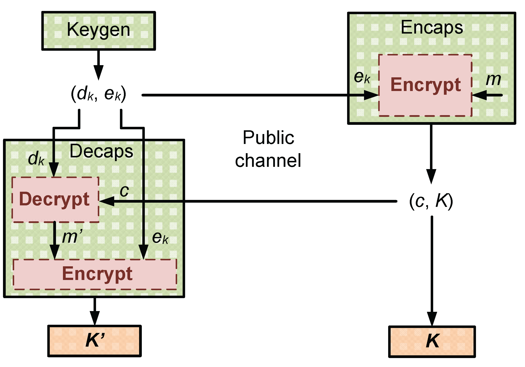
Figure 2.
The proposed SoC architecture with NTT accelerator.
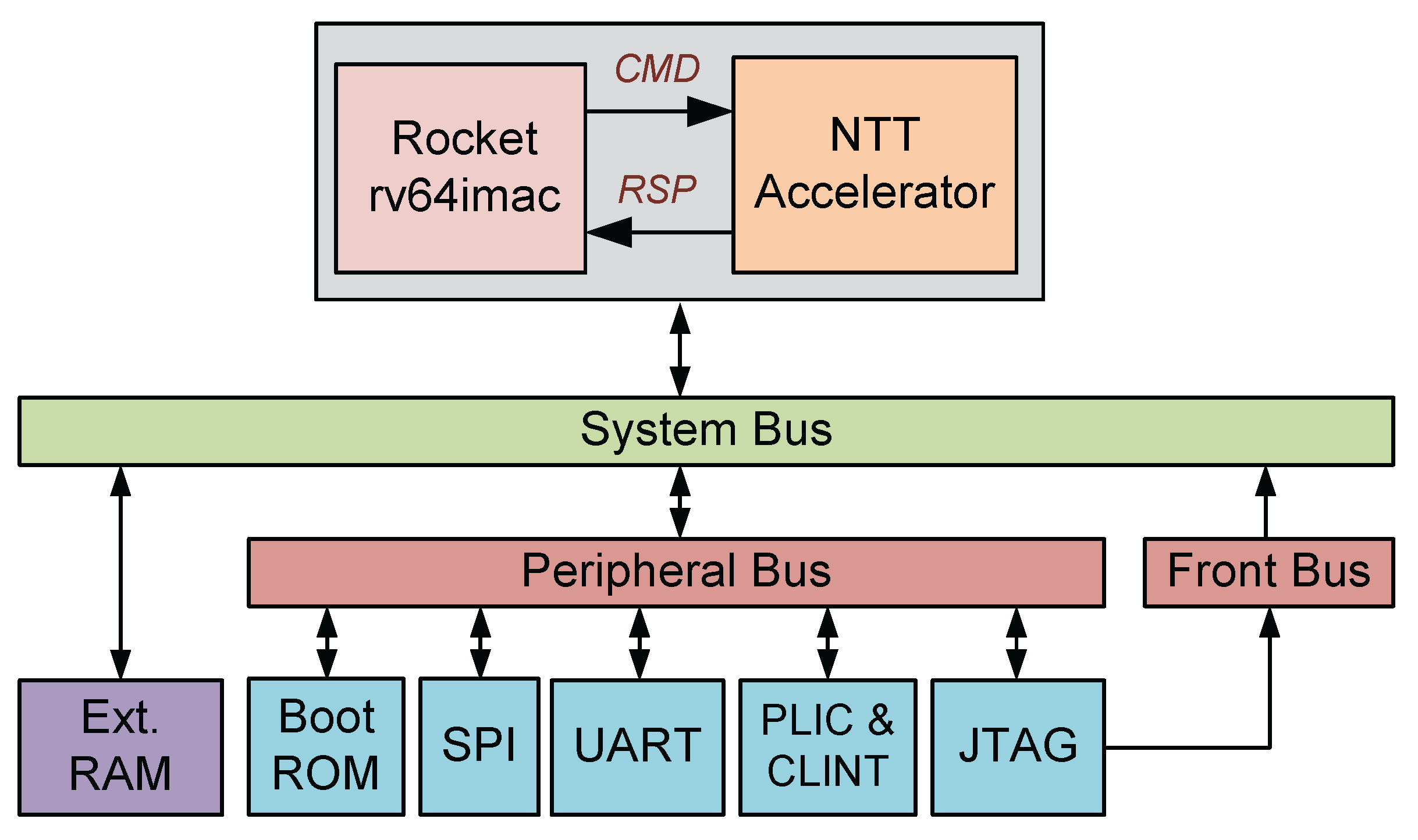
Figure 3.
Interface between CPU and NTT accelerator.
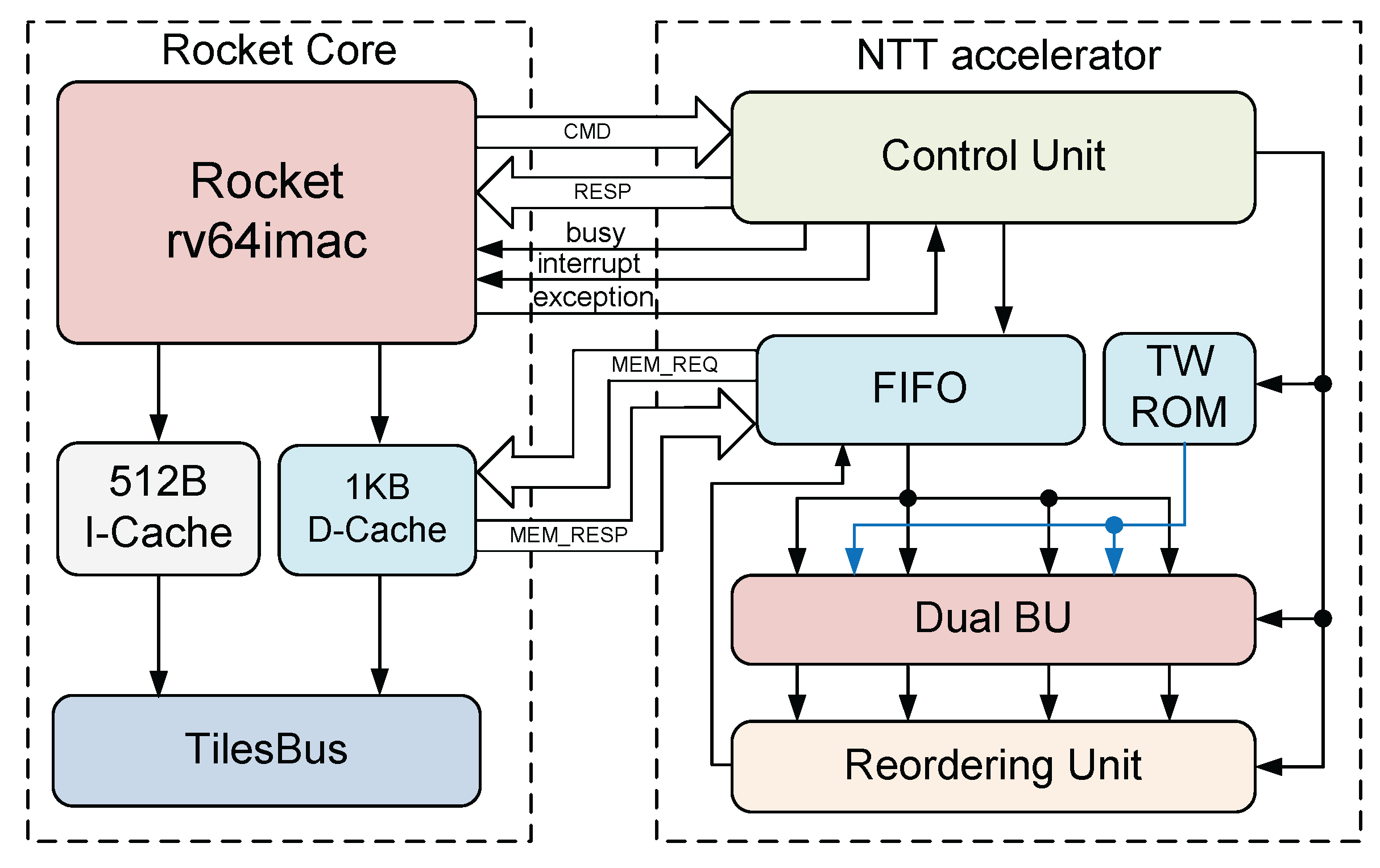
Figure 4.
The RISC-V custom instruction architecture.
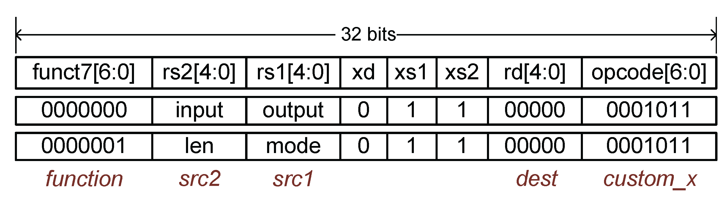
Figure 5.
The accelerator’s execution after getting custom instructions.
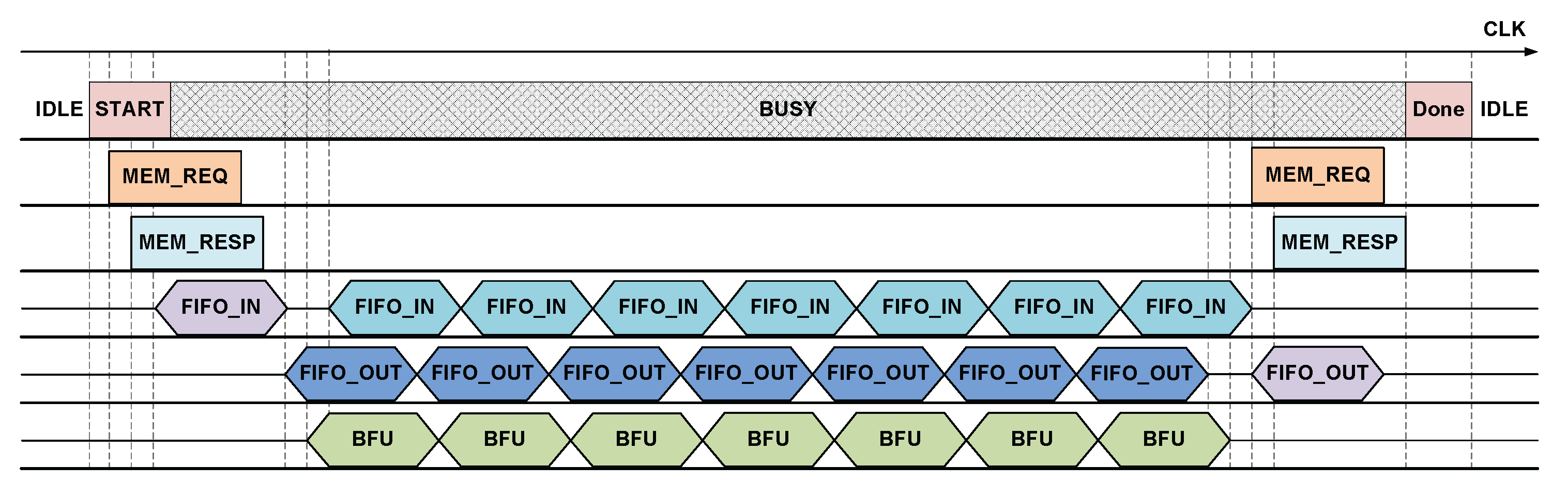
Figure 6.
The NTT tightly-coupled accelerator architecture.
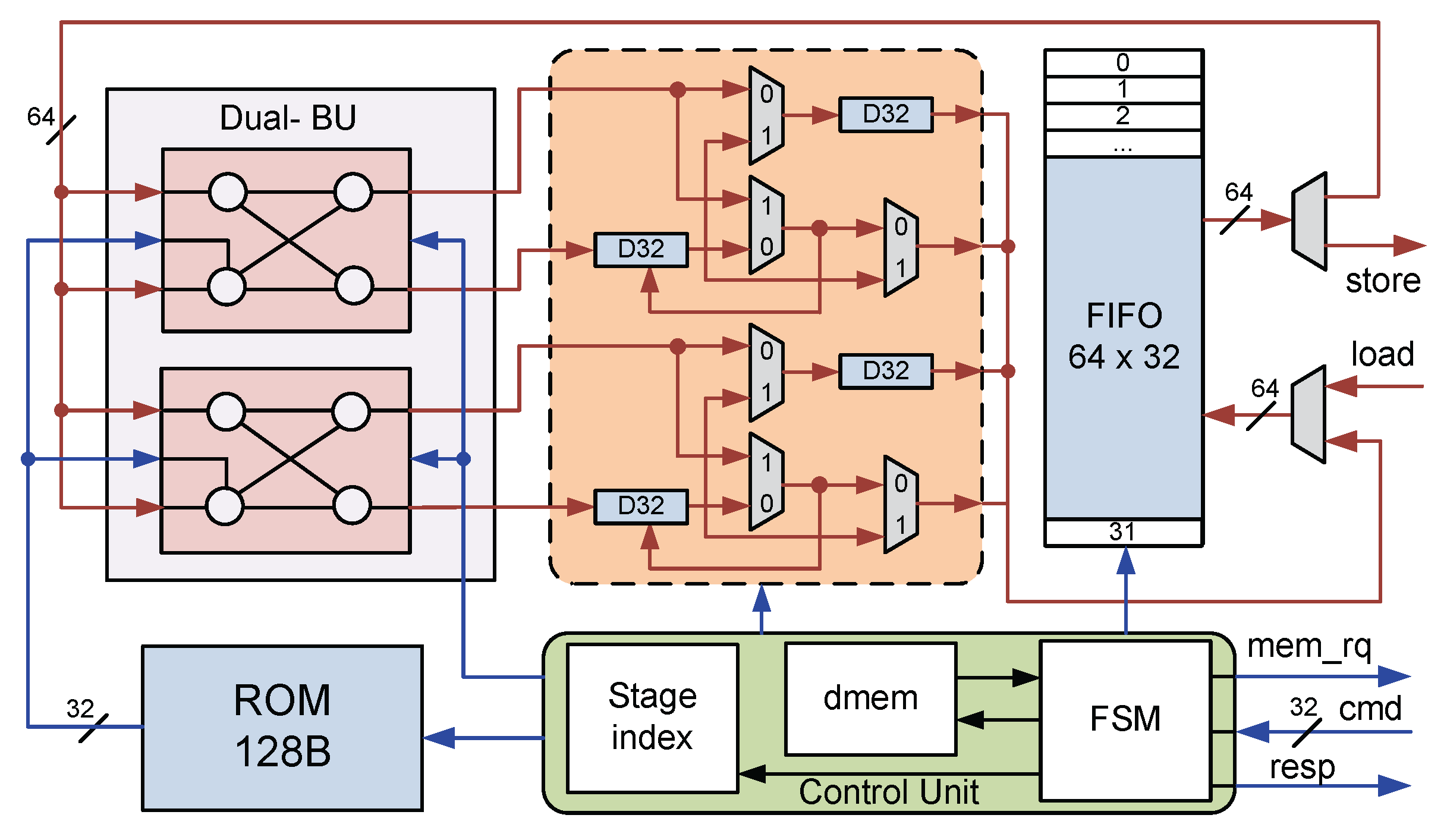
Figure 7.
CMOS 180nm chip micrograph.
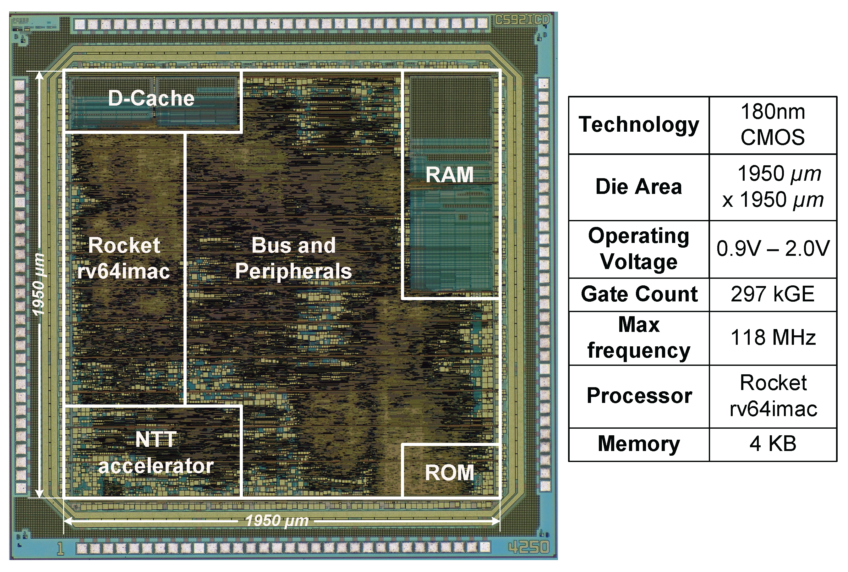
Figure 8.
Speedup efficiency comparison of the algorithm implementation compared to the C baseline.
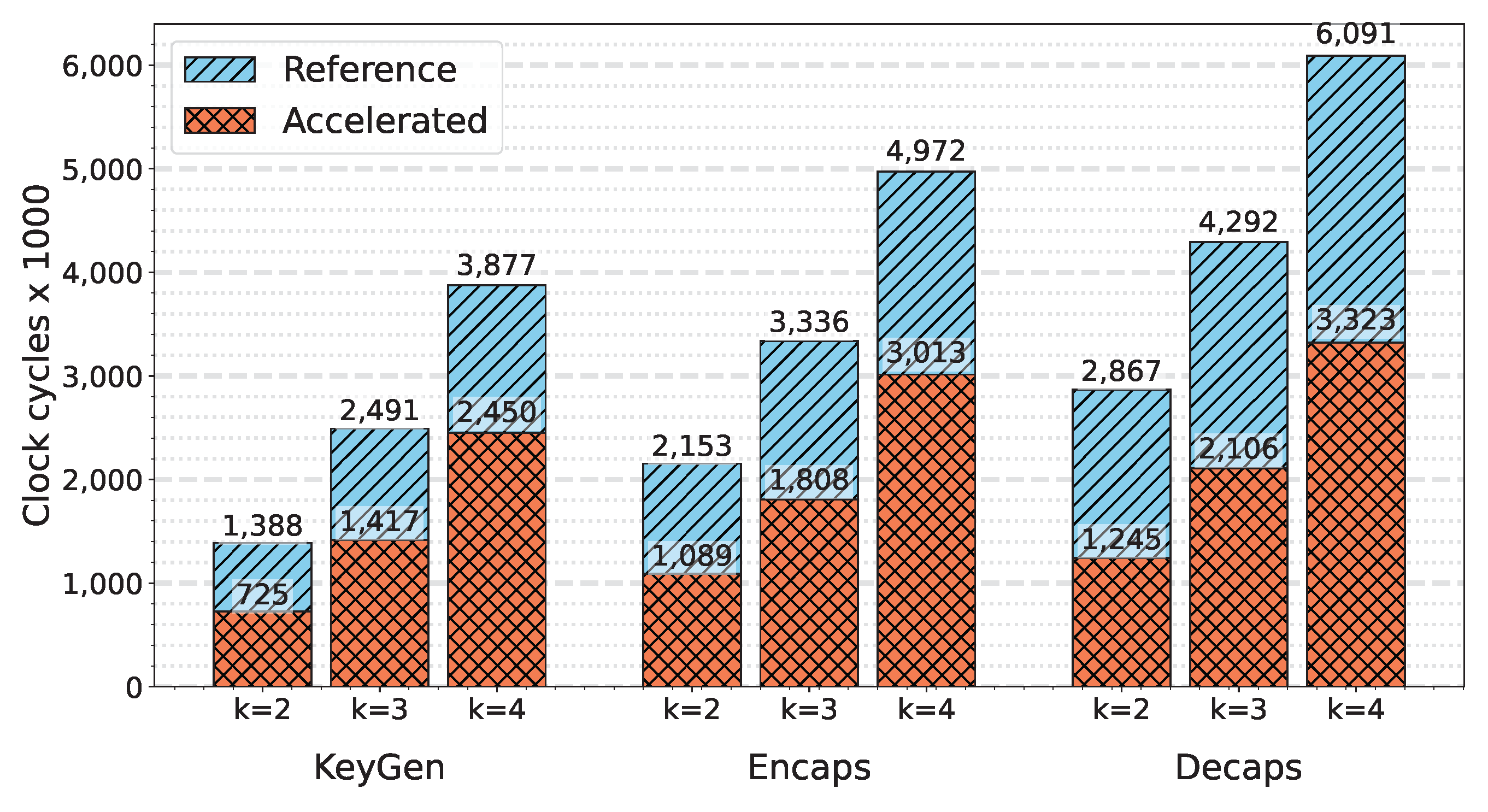
Figure 9.
The acceleration efficiency of the systems after improvements compared to the C baseline.
Disclaimer/Publisher’s Note: The statements, opinions and data contained in all publications are solely those of the individual author(s) and contributor(s) and not of MDPI and/or the editor(s). MDPI and/or the editor(s) disclaim responsibility for any injury to people or property resulting from any ideas, methods, instructions or products referred to in the content. |
© 2025 by the authors. Licensee MDPI, Basel, Switzerland. This article is an open access article distributed under the terms and conditions of the Creative Commons Attribution (CC BY) license (http://creativecommons.org/licenses/by/4.0/).
Copyright: This open access article is published under a Creative Commons CC BY 4.0 license, which permit the free download, distribution, and reuse, provided that the author and preprint are cited in any reuse.


