
Submitted:
12 November 2025
Posted:
17 November 2025
You are already at the latest version
Abstract
A novel precision operational amplifier scheme has been developed and investigated, implemented using complementary bipolar transistors and input field-effect transistors controlled by a p-n junction. Computer simulation of the developed circuit was performed in LTSpice environment, which demonstrates that the proposed schematic solution provides a high voltage gain (over 80 dB) with low static current consumption and relatively low load resistances (RL = 2 kΩ). The systematic component of the zero voltage offset does not exceed 100 µV.
Keywords:
operational amplifier
; complementary bipolar transistors
; input field-effect transistor controlled by a p-n junction
; systematic component of zero voltage offset
; voltage gain coefficient
1. Introduction
An operational amplifier (op amp) with input junction-gate field effect transistors (JFETs) is a fundamental functional block in many radio-electronic systems. Currently, leading microelectronics companies are mass-producing op amps with input JFETs such as AD8244, AD8625, AD8220 (Analog Devices), and WSH223 (Tesla). In many cases, there is a need for precision operational amplifiers with small input zero voltage offset (V0) [1].
The input zero voltage offset (V0) of classical direct-coupled operational amplifiers consists of two main components.
where VOS.1 – the schematic contribution to V0, whose numerical values depend on the quality of implementation of op amps functional blocks and relate to the influence of the following factors on VOS.1:
- -
- voltage asymmetry in the collector–base bias conditions of the dominant transistor pair;
- -
- internal feedback factors in transistors caused by the Early effect;
- -
- base current gain coefficients (β) of bipolar transistors, which in many cases have relatively low values (β=50-200).
In equation (1), VOS.2 represents the process-related component, which depends on transistor fabrication tolerances, their design features and layout rules, the presence of temperature gradients across the elements of the input differential pair, etc. Various methods are effectively employed to reduce the process-related offset voltage component VOS.2 [2,3,4]. Achieving low VOS.2 value falls within the responsibility of process engineers and specialists in semiconductor device physics.
A significant disadvantage of the classic differential operational amplifier (Figure 1), which was selected for comparison with the proposed operational amplifier, is that it exhibits elevated values of the systematic component of the input offset voltage. This is caused by the implementation of inefficient circuit design solutions. At the same time, as simulation shows, the circuit-induced component VOS.1 in the conventional circuit amounts to several millivolts.
In practical op amp circuits, the numerical values of the circuit-induced offset voltage component VOS.1 in equation (1) dominate, necessitating specialized design of their fundamental functional blocks. Minimization of VOS.1 falls within the responsibility of circuit designers developing operational amplifiers. The proposed op amp addresses this class of problems and enhances the performance parameters of differential stages implemented with field-effect transistors (FETs) [5,6,7,8,9,10,11,12,13].
2. Analysis of the Basic Scheme of the Proposed Op Amp
Figure 2 shows the circuit diagram of the proposed precision operational amplifier [14], which is implemented using complementary n-p-n and p-n-p bipolar transistors, as well as input junction field-effect transistors (JFETs). This integrated fabrication process has been adopted by several microelectronics companies, including the Novosibirsk Semiconductor Devices Factory “Vostok.”. At the same time, the systematic component of the zero offset voltage is significantly reduced in the developed circuit, and the effect of the current gain coefficients of the base of bipolar transistors on VOS.1 is minimized. In addition, the circuit of the proposed op amp is characterized by the effect of reducing the effect of the low-resistance load resistance of the op-amp on its open voltage gain.
The DC operating point of the transistors in the circuit of Figure 2 is set by reference current sources (I1=I2=2I0), which in practical implementations are realized using n-JFET transistors.
According to Kirchhoff’s current law, with bias currents I1=I2=2I0, the base, emitter, and collector currents of bipolar transistors Q1–Q6 shown in Figure 2 are established as indicated.
It also follows from Figure 2 that at the high-impedance node Σ1, the sum of the currents flowing into this node is equal to the sum of the currents flowing out, i.e., the current error at the high-impedance node is zero. This is a necessary condition for minimizing the circuit component of the zero bias voltage VOS.1 in formula (1). This conclusion is confirmed by computer simulation of the circuit shown in Figure 3, where VOS.1 = 65.7µV. The open-loop gain of the op amp with a high-impedance load is close to 90 dB (Figure 4).
3. Results of Computer Simulation
Figure 3 presents the DC operating point of the operational amplifier transistors (a) as well as the logarithmic amplitude-frequency plot of the voltage gain (b) of the operational amplifier, which is illustrated in Figure 2, within the LTSpice environment. The analysis is conducted under the following conditions: I1=I2=200μA, V4 (VDN)=4.5V, temperature (t°=27°C), and supply voltages Vcc=Vee=±10V.
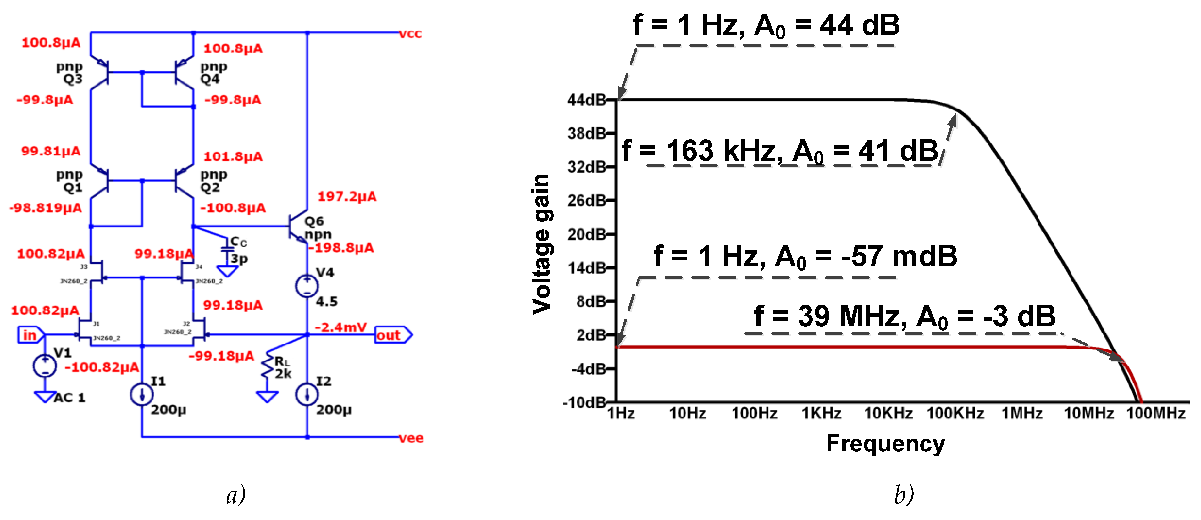
In the proposed op amp topology, the influence of the load resistance RL the voltage gain is minimized. As demonstrated by the simulations in Figure 4a and Figure 4b for RL =2kΩ, the voltage gain coefficient of the op amp (Figure 2) remains virtually unchanged - close to 90 dB - compared to the case of an infinite load resistance (RL =∞).
Figure 4 illustrates the DC operating point for the transistors (a) and the logarithmic amplitude-frequency characteristic of the voltage gain (b) for the developed operational amplifier (Figure 2). The analysis is conducted under the following conditions: I1 and I2 are set at 200 μA, V4 (VDN) is 4.5 V, compensation capacitor CC is 3 pF, the ambient temperature is 27°C, the supply voltages Vcc and Vee are ±10 V, and the load impedance is relatively low at 2 kΩ.
Figure 5 shows the DC operating point of transistors (a) and the logarithmic amplitude-frequency response (b) of the classic op amp circuit (Figure 1) at I1=I2=200 μA, V4(VDN)=4.5V, CC=3pF, t°=27°C, Vcc=Vee=±10V and high-impedance load (RL=∞).
Figure 5 presents a comprehensive DC operating point analysis of the transistors, as well as the logarithmic amplitude-frequency response, for the classic operational amplifier circuit depicted in Figure 1. This analysis is conducted under a set of conditions, including I1=I2=200μA for equal current sources, V4 (VDN)=4.5V for the input voltage, CC=3pF, t°=27°C for operating temperature, Vcc=Vee =±10V for the supply voltages, and a high-impedance load (RL =∞).
Figure 6 demonstrates the DC operating points (a) and the logarithmic amplitude-frequency characteristic of the voltage gain (b) for the transistors within the standard operational amplifier circuit shown in Figure 1. The conditions are established with a current I1=I2 set at 200 μA, a voltage V4 (VDN) of 4.5V, a capacitor CC with a capacitance of 3pF, at a temperature of 27°C, and utilizing a supply voltage of ±10V. The load impedance is configured at RL =2 kΩ, which is relatively low.
Thus, comparative modeling of two op-amps shown in Figures 7 and 8, as well as Figures 9 and 10 shows that in the absence of the bipolar transistor Q5 in the circuit (as is done in Figure 9), the voltage gain of the op amp at RL = 2 kΩ decreases by 45 dB, i.e. by more than two orders of magnitude. In addition, the proposed op-amp circuit creates conditions under which the current error in the high-impedance node Σ1 is minimized, since here:
where Ic.2=2I0+2Ib.b – DC current of the bipolar transistor Q2 collector;
Ib.6=2Ib.b – DC current of the bipolar transistor Q6 base;
Id.10=I0 – DC drain current of the Q10 output field-effect transistor with a control p-n junction.
This allows us to obtain small values of VOS.1 in formula (1), which is confirmed by the results of computer modeling in Figure 3, Figure 5, where VOS.1 = 65-70 μV.
The proposed op amp circuit is shown in Figure 2 and is also characterized by an increased level of voltage gain A0 (about 90 dB) at a load resistance of 2 kΩ, which is more than two orders of magnitude higher than A0 in the op amp circuit (Figure 9, Figure 10).
Thus, the proposed op amp has significant advantages in comparison with the known circuit design (Figure 1).
4. Conclusion
A precision operational amplifier circuit has been developed and investigated, which can be implemented based on technological processes implementing n-JFET transistors, as well as p-n-p and n-p-n bipolar transistors. Comparative modeling of the proposed circuit and op-amp with a typical circuit design shows that the new circuit provides a higher gain (by 40 dB), can operate at relatively low load resistances, and provides a low level of the systematic component of the zero offset voltage (less than 100 μV).
The research has been carried out at the expense of the Grant of the Russian Science Foundation (project No. 23-79-10023), https://rscf.ru/en/project/23-79-10023/.
References
- Carter, B., & Mancini, R. Op Amps for Everyone. Translated from English by A. N. Rabodzey. Moscow: Dodeka-XXI, 2011. 544 p. (Schematic Design Series). Includes English title page. ISBN 978-5-94120-242-3.
- Borkar; Shekhar Y. et al. Transistor group mismatch detection and reduction. US Patent 6272666, 2001-08-07.
- Hart; Michael L. et al. Method and apparatus for compensating for process variations. US Patent 7453311, 2008-11-18.
- Horowitz, P., & Hill, W. The Art of Electronics. 2nd ed. Translated from English. Moscow: BINOM Publishing, 2014. 704 p.
- Bugakova, A. V., Prokopenko, N. N., Dvornikov, O. V., & Drozdov, D. G. Differential Amplifier Based on Complementary Junction Field-Effect Transistors. Patent RF No. 2736412, Int. Cl. H03F 3/34, H03F 3/45; application No. 2020115040/08; filed April 29, 2020; published November 17, 2020, Bull. No. 32. Applicant: Don State Technical University (DSTU).
- Prokopenko, N. N., Dvornikov, O. V., & Pakhomov, I. V. Input Differential Stage Based on Complementary Junction Field-Effect Transistors for Low-Temperature Operation. Patent RF No. 2712416, Int. Cl. H03F 3/00; application No. 2019122270/08; filed July 16, 2019; published January 28, 2020, Bull. No. 4. Applicant: Don State Technical University (DSTU).
- Chumakov, V. E., Prokopenko, N. N., Kunts, A. V., & Bugakova, A. V. Differential Amplifier Based on Gallium Arsenide Field-Effect Transistors. Patent RF No. 2770912, Int. Cl. H03F 3/45; application No. 2021129177; filed October 6, 2021; published April 25, 2022, Bull. No. 12. Applicant: Don State Technical University (DSTU).
- Sergeenko, M. A., Chumakov, V. E., Dvornikov, O. V., & Prokopenko, N. N. Precision Gallium Arsenide Operational Amplifier with Low Systematic Input Offset Voltage and High Voltage Gain. Patent RF No. 2813370, Int. Cl. H03F 3/45; application No. 2023130248; filed November 21, 2023; published February 12, 2024, Bull. No. 5. Applicant: Don State Technical University (DSTU).
- Prokopenko, N. N., Dvornikov, O. V., Bugakova, A. V., & Pakhomov, I. V. Differential Operational Amplifier. Patent RF No. 2616573, Int. Cl. H03F 3/45; application No. 2015149078/08; filed November 16, 2015; published April 17, 2017, Bull. No. 11. Applicant: Don State Technical University (DSTU).
- Bugakova, A. V., Zhuk, A. A., & Prokopenko, N. N. Differential Amplifier Based on Complementary Junction Field-Effect Transistors. Patent RF No. 2688225, Int. Cl. H03F 3/34, H03F 3/45; application No. 2018126843/08; filed July 23, 2018; published May 21, 2019, Bull. No. 15. Applicant: Don State Technical University (DSTU).
- Prokopenko, N. N., Zhuk, A. A., Bugakova, A. V., & Pakhomov, I. V. Differential Stage Based on Complementary JFETs with Enhanced Common-Mode Input Signal Rejection. Patent RF No. 2710296, Int. Cl. H03F 1/00, H03F 3/34; application No. 2019131161/08; filed October 3, 2019; published December 25, 2019, Bull. No. 36. Applicant: Don State Technical University (DSTU).
- Prokopenko, N. N., Budyakov, P. S., & Pakhomov, I. V. Differential Amplifier Based on Complementary Field-Effect Transistors with Improved DC Operating Point Stability. Patent RF No. 2710930, Int. Cl. H03F 3/34, H03F 3/45; application No. 2019122165/08; filed July 15, 2019; published January 14, 2020, Bull. No. 2. Applicant: Don State Technical University (DSTU).
- Prokopenko, N. N., Drozdov, D. G., & Zhuk, A. A. Class AB Differential Stage Based on Complementary Junction Field-Effect Transistors for Low-Temperature Operation. Patent RF No. 2710847, Int. Cl. H03F 3/34; application No. 2019126326/08; filed August 21, 2019; published January 14, 2020, Bull. No. 2. Applicant: Don State Technical University (DSTU).
- Pakhomov, I. V., Titov, A. E., Chumakov, V. E., & Prokopenko, N. N. Precision Operational Amplifier Based on Complementary Bipolar and Input Junction Field-Effect Transistors. Russian Patent Application No. 2025128076, filed October 08, 2025.
Figure 1.
Circuit diagram of a classic differential operational amplifier (Motorola (USA) patent US 4,042,886, 1975).
Figure 1.
Circuit diagram of a classic differential operational amplifier (Motorola (USA) patent US 4,042,886, 1975).
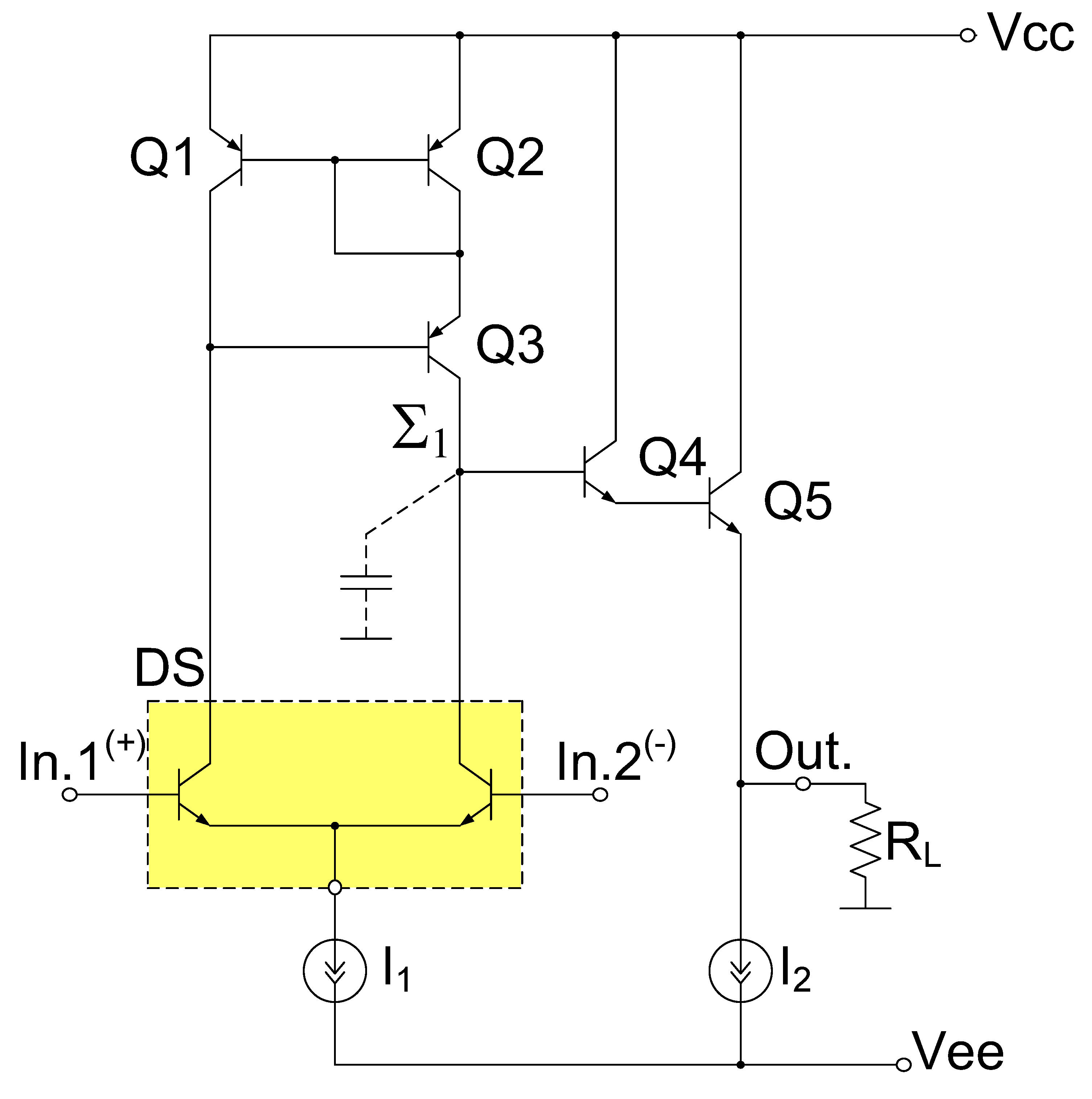
Figure 2.
Circuit diagram of the proposed complementary BJT and n-JFET op amp with a single high-impedance node (Σ1).
Figure 2.
Circuit diagram of the proposed complementary BJT and n-JFET op amp with a single high-impedance node (Σ1).
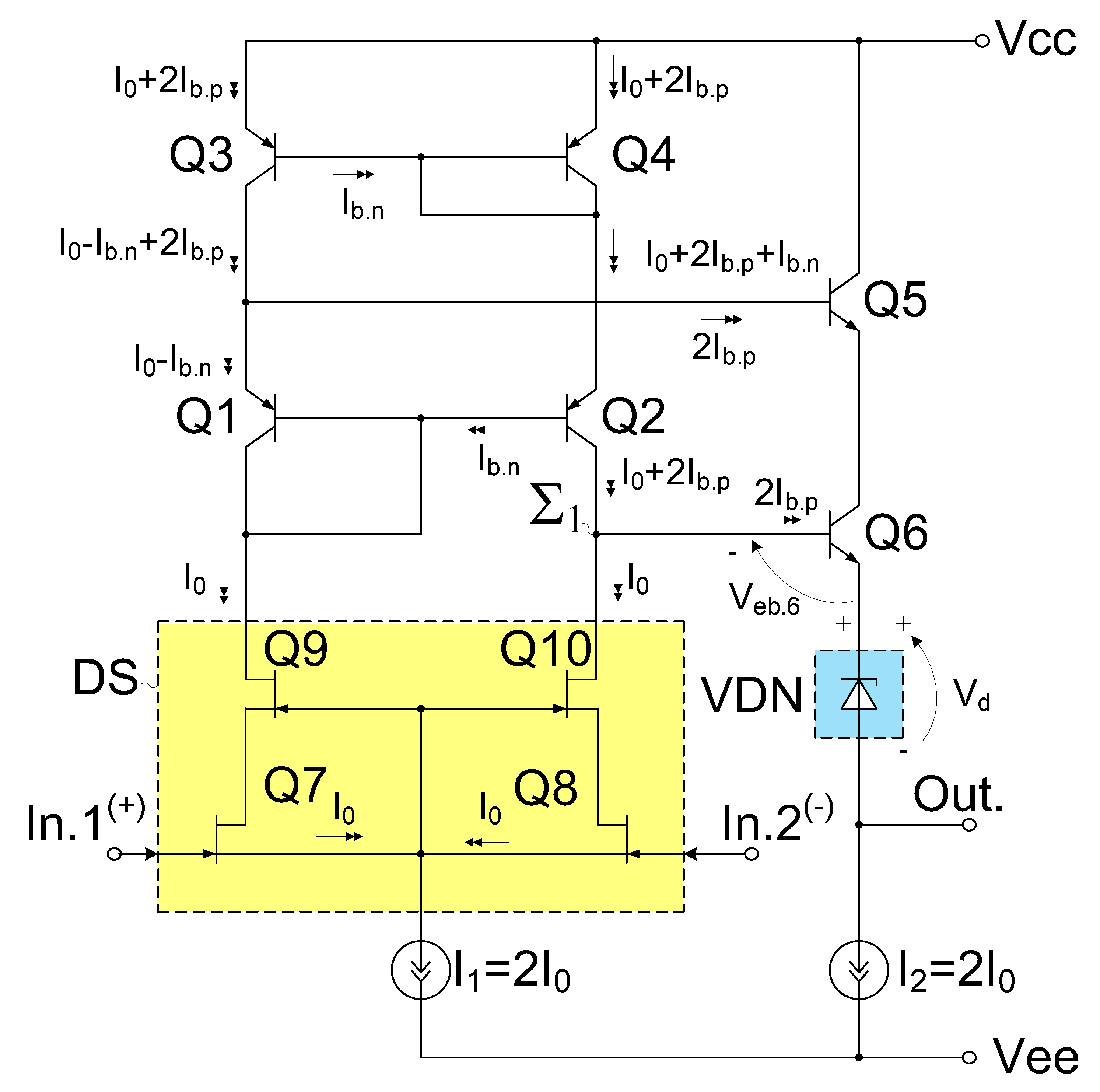
Figure 3.
DC operating point of the transistors in the op amp (a); logarithmic amplitude-frequency characteristic of the voltage gain coefficient of the op amp(b).
Figure 3.
DC operating point of the transistors in the op amp (a); logarithmic amplitude-frequency characteristic of the voltage gain coefficient of the op amp(b).
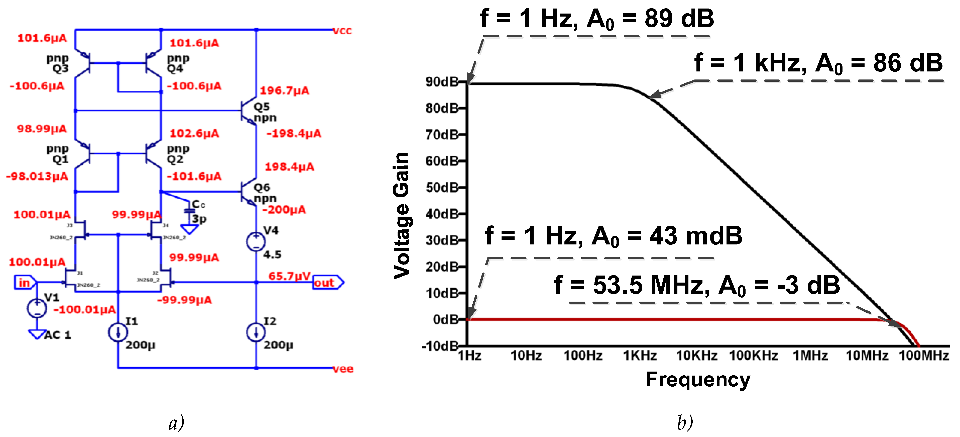
Figure 4.
DC operating point of transistors (a); The logarithmic amplitude-frequency characteristic plot of the voltage gain (b).
Figure 4.
DC operating point of transistors (a); The logarithmic amplitude-frequency characteristic plot of the voltage gain (b).
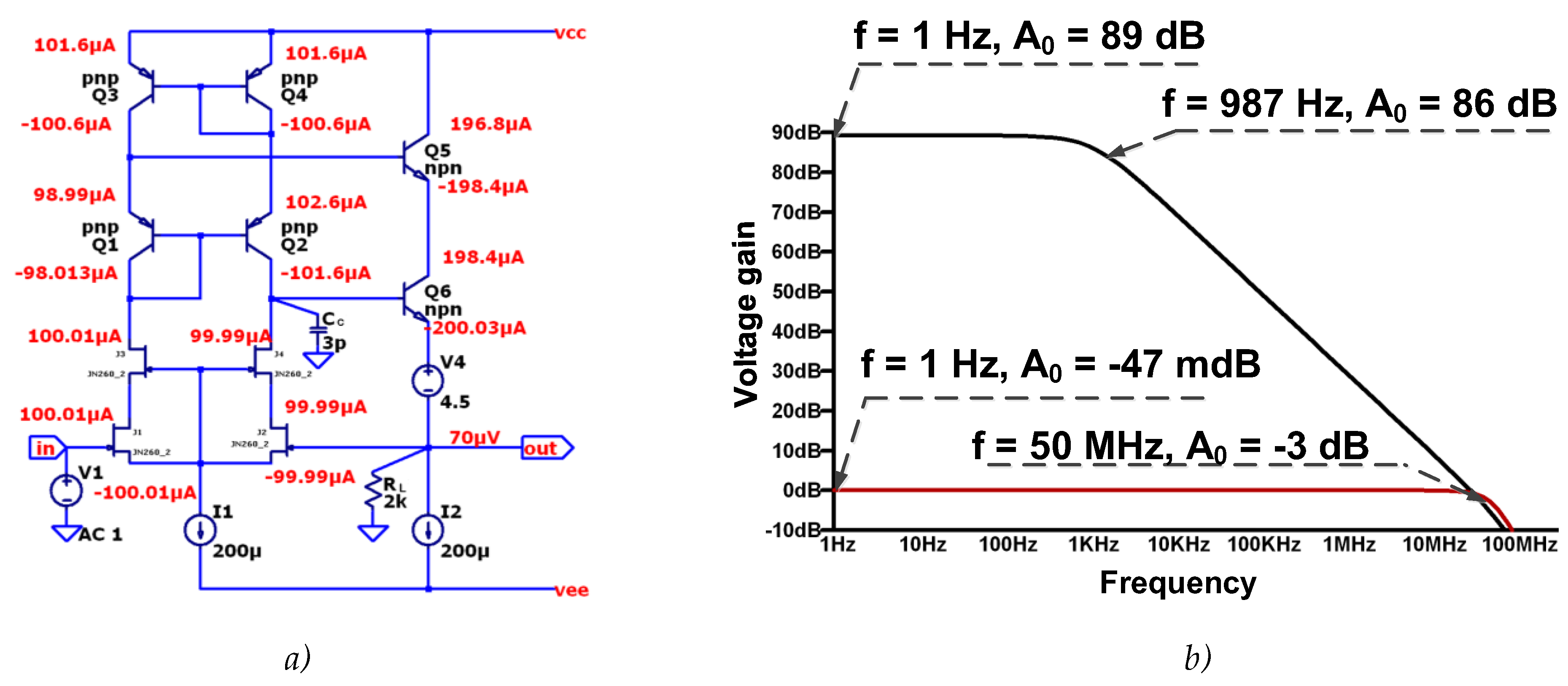
Figure 5.
DC operating point of transistors (a); Logarithmic amplitude-frequency characteristic of the voltage gain (b).
Figure 5.
DC operating point of transistors (a); Logarithmic amplitude-frequency characteristic of the voltage gain (b).
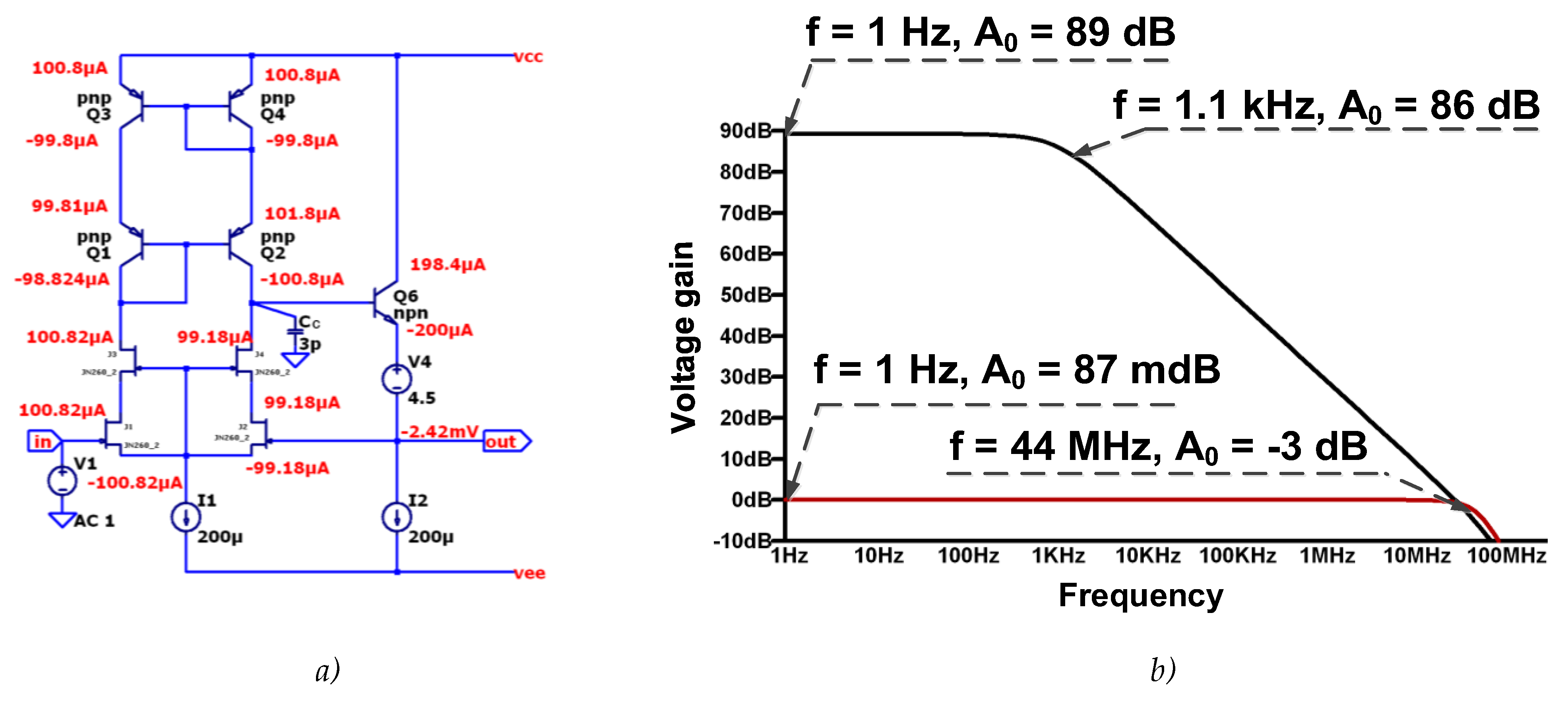
Figure 6.
DC operating point of transistors (a); Logarithmic amplitude-frequency characteristic of the voltage gain (b).
Figure 6.
DC operating point of transistors (a); Logarithmic amplitude-frequency characteristic of the voltage gain (b).
Disclaimer/Publisher’s Note: The statements, opinions and data contained in all publications are solely those of the individual author(s) and contributor(s) and not of MDPI and/or the editor(s). MDPI and/or the editor(s) disclaim responsibility for any injury to people or property resulting from any ideas, methods, instructions or products referred to in the content. |
© 2025 by the authors. Licensee MDPI, Basel, Switzerland. This article is an open access article distributed under the terms and conditions of the Creative Commons Attribution (CC BY) license (http://creativecommons.org/licenses/by/4.0/).
Copyright: This open access article is published under a Creative Commons CC BY 4.0 license, which permit the free download, distribution, and reuse, provided that the author and preprint are cited in any reuse.


