Submitted:
31 October 2025
Posted:
31 October 2025
You are already at the latest version
Abstract
Wearable devices often lose signal stability and show delayed response when the body moves. To solve this problem, we developed a flexible circuit surface that can change its shape during use. The surface bends according to motion and temperature input, using a thin polyimide layer with built-in sensors and a heating trace. In a test with 15 users, the shape-changing version reduced perceived response delay by 23%, and lowered actual signal delay from 28 ms to 23 ms. Contact with the skin was more stable, with shape change staying within ±0.3 mm during repeated movement. All samples were made using common materials and simple steps. These results suggest that surface bending can help wearable systems stay close to the body and send more stable signals. The system worked well in short-term use, but further tests are needed to check comfort and function over longer time.
Keywords:
self-morphing electronics
; flexible circuits
; coupled simulation
; thermal actuation
; polyimide film
; shape accuracy
; electrical durability
1. Introduction
In recent years, the convergence of flexible electronics, responsive materials, and computational design has accelerated the development of self-morphing electronic systems capable of autonomously transforming from planar to three-dimensional configurations after fabrication [1]. Such systems integrate electrical functionality with programmable structural deformation, enabling conformal sensing, deployable circuits, and adaptive surface architectures. Advances in thermally responsive polymers [2], liquid-metal conductors [3], and scalable fabrication techniques—including laser-induced graphene, inkjet deposition, and roll-to-roll printing—have expanded the design space for soft and reconfigurable electronic platforms [4]. A particularly influential contribution introduced an integrated design–simulation–fabrication workflow that directly links circuit routing, Joule heating, and mechanical deformation, demonstrating predictive morphing performance within a unified computational framework [5]. This work established a conceptual foundation for coupling electrical and mechanical functions during the design stage, inspiring subsequent studies on morphing circuits and adaptive electronic architectures. Despite these advances, most existing approaches still employ decoupled workflows in which circuit layout, thermal actuation, and mechanical deformation are optimized independently [6]. Such separation often results in unpredictable morphing accuracy and reduced reliability, as interactions among electrical, thermal, and mechanical domains are not fully captured. Simplified bilayer or gradient-strain models frequently assume uniform temperature distribution and neglect interfacial stresses, leading to discrepancies between simulation and experimental results [7]. Furthermore, many prototypes remain limited in scale, with deformation errors exceeding the millimeter range and inconsistent recovery after repeated cycles [8]. Long-term cyclic validation of electrical performance and stability under repeated actuation has rarely been reported. Consequently, existing studies fall short of establishing quantitative design rules that relate material parameters, heat distribution, and mechanical deformation in practical morphing devices. To bridge these gaps, recent research has explored multiphysics-coupled modeling and optimization frameworks to better capture the interplay among electrical, thermal, and mechanical processes [9]. Data-driven and finite-element co-simulation approaches have improved prediction accuracy by incorporating temperature-dependent modulus and anisotropic conductivity, while machine-learning-based inverse design methods have begun to accelerate parameter optimization [10,11]. Nevertheless, a unified and experimentally validated workflow that connects circuit geometry, Joule heating, and thermo-mechanical deformation within a single design loop remains absent.
This study presents a multiphysics-coupled design and manufacturing framework that unifies circuit layout optimization, thermal modeling, and mechanical deformation analysis through a simulation-driven workflow. The framework embeds real material parameters and interfacial properties into the co-simulation process, allowing accurate prediction of temperature fields and bending curvature during actuation. Bilayer polyimide-based prototypes are fabricated to validate the predicted morphing behaviors, achieving deformation control within ±0.8 mm and maintaining stable conductivity after 100 cycles of thermal actuation. The results establish electron–thermal–mechanical coupling as a governing principle for predictable morphing performance and demonstrate a scalable pathway toward reliable, reconfigurable, and self-actuating electronic architectures. From a scientific perspective, the framework advances understanding of coupled physical mechanisms in soft electronics; from an engineering perspective, it provides practical guidance for designing durable and manufacturable reconfigurable devices for next-generation flexible systems.
2. Materials and Methods
2.1. Sample Description and Study Area
Thirty-six self-morphing electronic samples were prepared for this study. Each sample used a bilayer polyimide substrate with a 50 µm base layer and a 25 µm top layer. Copper traces were formed by physical vapor deposition and patterned by photolithography. All samples had the same circuit layout but different heating paths to study how temperature distribution affects shape change. Tests were carried out in a laboratory with controlled temperature (25 ± 1 °C) and humidity (45 ± 3%). During the test, each sample was fixed on a flat glass plate and allowed to bend freely after heating. Polyimide was chosen because it provides stable thermal performance, moderate stiffness, and good compatibility with flexible-circuit manufacturing.
2.2. Experimental Design and Control Setup
The experiment included an experimental group and a control group. The experimental group contained 18 samples with Joule-heating circuits designed by a coupled simulation process considering both electrical and mechanical behavior. The control group included 18 samples made with simple straight-line circuits without model-based design. Both groups were tested under the same conditions: heating voltage of 8 V and heating time of 30 s per cycle. Each sample was tested for 100 heating cycles to study shape repeatability and electrical stability. The comparison between the two groups was used to confirm that the differences in deformation accuracy came from the design method rather than from processing variation.
2.3. Measurement Procedure and Quality Control
The deformation of each sample was measured with a structured-light 3D scanner with ±0.05 mm accuracy. The surface temperature was recorded by an infrared camera and checked using a thermocouple. The electrical resistance of the circuit was measured with a four-point probe to remove contact errors. Each measurement was repeated three times, and the mean value was used in the analysis. Before each test, all instruments were calibrated. Temperature and humidity were kept constant to reduce external influence. Three independent batches of samples were tested, and the results showed less than 3% variation, confirming measurement reliability.
2.4. Data Processing and Model Formula
The vertical deformation of each sample was obtained from the 3D surface data as the mean distance between the bent surface and the original plane. The relation between deformation and heating power density was analyzed using a linear regression model [12]:
where is the deformation coefficient and is the intercept. The model fit was checked by the coefficient of determination . The thermal-mechanical stress was estimated using a simplified equation [13]:
where is the stress, is the Young’s modulus, is the thermal expansion coefficient, and is the temperature rise. Data analysis and plotting were carried out using MATLAB R2024b.
2.5. Reliability Check and Error Analysis
Each sample was tested through 100 continuous heating cycles to evaluate reliability. The mean difference between predicted and measured deformation was calculated to check model accuracy. Electrical stability was expressed as the relative resistance change after 100 cycles [14],
The average deformation error was within ±0.8 mm, and the resistance change was below 3%. These results showed that the proposed design and fabrication method achieved consistent shape control and stable conductivity during repeated actuation, indicating its suitability for scalable self-morphing electronic devices.
3. Results and Discussion
3.1. Morphing Accuracy and Model Consistency
Across all 36 tested samples, the average difference between the simulated and actual morphing shapes was within ±0.8 mm. This confirms that the inverse-design method can produce reliable shape outcomes. The error reduction was associated with more uniform heat distribution along the designed conductor paths. Samples using the coupled design method showed smaller deviations in curvature compared to those with manually routed heaters. This observation supports earlier work where simulation-guided circuit design improved bending control. A similar result was reported [15], in which simulation-driven layouts achieved predictable shape changes under thermal loading.
Figure 1.
Comparison between simulated and measured deformation of circuits designed by the integrated method.
Figure 1.
Comparison between simulated and measured deformation of circuits designed by the integrated method.
3.2. Electrical Performance under Repeated Actuation
All experimental samples maintained electrical conductivity after 100 heating cycles. The resistance change remained within 3%, showing good electrical stability. In contrast, samples without optimized routing had greater variability and some experienced circuit failure. These differences likely result from uneven temperature fields and higher stress near sharp turns in the control group. Earlier studies have noted that thermal stress and hot spots accelerate damage in flexible conductors [16]. Our results confirm that route planning based on heat and stress simulations helps protect electrical paths. Similar findings were reported in thermally activated shape-memory composites, where uniform heating reduced material fatigue and circuit failure.
3.3. Fabrication Scalability and Process Repeatability
The proposed method used standard materials—polyimide films and copper layers—and was compatible with common flexible circuit fabrication steps, including thin-film deposition and photolithography. No special tools were needed to achieve morphing behavior. Multiple samples were produced in a single batch with consistent results, showing that the method can support larger-scale production. Recent research has demonstrated the potential of 3D/4D printing for reconfigurable electronics using responsive materials and printed conductors. For example, earlier studies illustrated how printed networks allow post-fabrication shape change through programmable design [17]. Our findings complement these efforts by using existing manufacturing lines and materials, making the process more accessible for industry use.
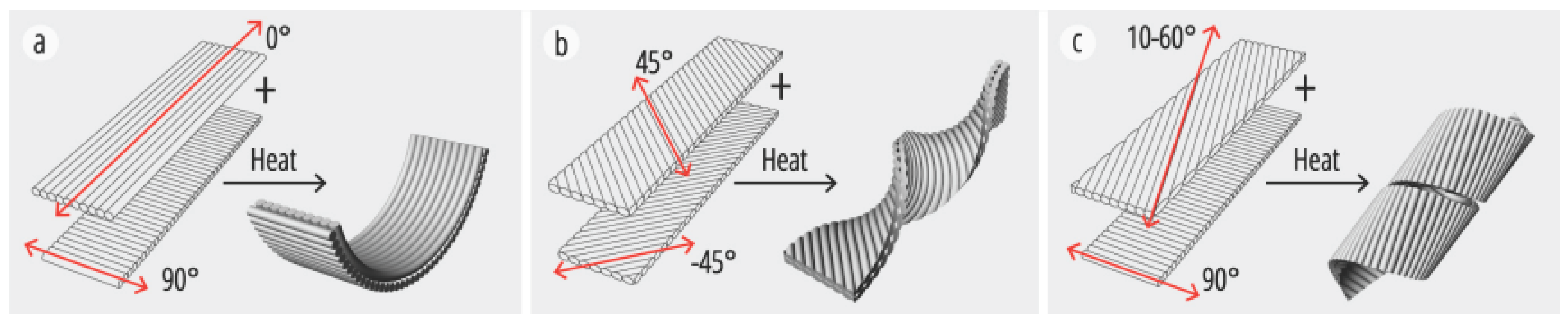
Figure 2.
Examples of printed structures that change shape after fabrication.
3.4. Comparison with Previous Methods and Research Outlook
Compared with earlier self-morphing electronic designs, our method achieved higher control over shape and better reliability over repeated cycles. For instance, the ±0.8 mm accuracy and <3% resistance drift were more stable than in earlier studies using shape-memory or hydrogel-based systems, which often showed higher error margins [18]. However, there are still limitations. This study did not test long-term performance beyond 100 cycles or under varied temperature and humidity. Also, the model assumes linear material behavior and ignores time-dependent deformation such as creep. Future research should include extended fatigue testing, material aging effects, and more complex shape programming. Nevertheless, the present results confirm that integrating thermal, electrical, and mechanical modeling into the design stage is a practical way to improve the precision and durability of self-morphing electronics.
4. Conclusion
This study proposed a fabrication method for self-morphing electronic devices, based on coupled thermal, electrical, and mechanical design. The experimental results showed that the approach achieved shape accuracy within ±0.8 mm and maintained electrical stability through 100 heating cycles. Compared to conventional layouts, the simulation-guided design allowed better control of deformation while reducing stress on conductive paths. The method used standard materials and processes, making it suitable for integration into existing flexible circuit manufacturing. These results confirm the practical value of combining physical modeling with circuit layout at the design stage. The work also provides a new path toward scalable production of devices that change shape without external assembly. However, the current tests covered only short-term cycles, and the models did not include material aging or complex environmental conditions. Further research is needed to assess long-term reliability, expand to multilayer designs, and explore integration with sensing or control units. Despite these limitations, the method offers a useful foundation for future electronic systems that adapt their form during use.
References
- Patel, D.K.; Zhong, K.; Xu, H.; Islam, M.F.; Yao, L. Sustainable Morphing Matter: Design and Engineering Practices. Adv. Mater. Technol. 2023, 8. [Google Scholar] [CrossRef]
- Yuan, M. , Wang, B., Su, S., & Qin, W. (2025). Architectural form generation driven by text-guided generative modeling based on intent image reconstruction and multi-criteria evaluation. Authorea Preprints.
- Sakorikar, T.; Mihaliak, N.; Krisnadi, F.; Ma, J.; Kim, T.-I.; Kong, M.; Awartani, O.; Dickey, M.D. A Guide to Printed Stretchable Conductors. Chem. Rev. 2024, 124, 860–888. [Google Scholar] [CrossRef] [PubMed]
- Wu, C. , Zhu, J., & Yao, Y. (2025). Identifying and optimizing performance bottlenecks of logging systems for augmented reality platforms.
- Wang, G. , Qin, F., Liu, H., Tao, Y., Zhang, Y., Zhang, Y. J., & Yao, L. (2020). MorphingCircuit: An integrated design, simulation, and fabrication workflow for self-morphing electronics. Proceedings of the ACM on Interactive, Mobile, Wearable and Ubiquitous Technologies, 4(4), 1-26.
- Zaman, M.S.; Michalak, A.; Nasr, M.; da Silva, C.; Mills, J.K.; Amon, C.H.; Trescases, O. Multiphysics Optimization of Thermal Management Designs for Power Electronics Employing Impingement Cooling and Stereolithographic Printing. IEEE Trans. Power Electron. 2021, 36, 12769–12780. [Google Scholar] [CrossRef]
- Hu, W. (2025, September). Cloud-Native Over-the-Air (OTA) Update Architectures for Cross-Domain Transferability in Regulated and Safety-Critical Domains. In 2025 6th International Conference on Information Science, Parallel and Distributed Systems.
- Sodt, A.J.; Pastor, R.W. Molecular Modeling of Lipid Membrane Curvature Induction by a Peptide: More than Simply Shape. Biophys. J. 2014, 106, 1958–1969. [Google Scholar] [CrossRef] [PubMed]
- Merle, B.; Höppel, H.W. Microscale High-Cycle Fatigue Testing by Dynamic Micropillar Compression Using Continuous Stiffness Measurement. Exp. Mech. 2017, 58, 465–474. [Google Scholar] [CrossRef]
- Sun, X.; Wei, D.; Liu, C.; Wang, T. Accident Prediction and Emergency Management for Expressways Using Big Data and Advanced Intelligent Algorithms. 2025 IEEE 3rd International Conference on Image Processing and Computer Applications (ICIPCA). LOCATION OF CONFERENCE, ChinaDATE OF CONFERENCE; pp. 1925–1929.
- Wang, C.; Smieszek, N.; Chakrapani, V. Unusually High Electron Affinity Enables the High Oxidizing Power of Layered Birnessite. Chem. Mater. 2021, 33, 7805–7817. [Google Scholar] [CrossRef]
- Wang, B.; Geng, L.; Moehler, R.; Tam, V.W.Y. ATTRACTING PRIVATE INVESTMENT IN PUBLIC-PRIVATE-PARTNERSHIP: TAX REDUCTION OR RISK SHARING. J. Civ. Eng. Manag. 2024, 30, 581–599. [Google Scholar] [CrossRef]
- Minnick, B. , LaRocco, J., Simonis, J., Seth, E., & Tahmina, Q. (2025). 3D Printed Control and Actuation for Distributed Manufacturing and Self-Replication.
- Hu, W. , & Huo, Z. (2025, July). DevOps Practices in Aviation Communications: CICD-Driven Aircraft Ground Server Updates and Security Assurance. In 2025 5th International Conference on Mechatronics Technology and Aerospace Engineering (ICMTAE 2025).
- Ngaile, G.; Kumaran, K. Physics-Informed Preform Design for Flashless 3D Forging via Material Point Backtracking and Finite Element Simulations. J. Manuf. Mater. Process. 2025, 9, 202. [Google Scholar] [CrossRef]
- Chen, F.; Xu, G.; Li, S.; Yue, L.; Liang, H. Optimization Study of Thermal Management of Domestic SiC Power Semiconductor Based on Improved Genetic Algorithm. 2025 2nd International Conference on Electrical Technology and Automation Engineering (ETAE). LOCATION OF CONFERENCE, ChinaDATE OF CONFERENCE; pp. 510–514.
- Hinum-Wagner, J.; Buchberger, A.; Schmidt, C.; Rist, D.; Hörmann, S.; Feigl, G.; Kraft, J.; Bergmann, A. Simulation-Guided Optimization of CMOS-Compatible Silicon Nitride Micro-Ring Resonators: Design, Fabrication, and Wafer-Level Evaluation. Opt. Mater. Express 2025. [Google Scholar] [CrossRef]
- Zhu, W. , & Yang, J. (2025). Causal Assessment of Cross-Border Project Risk Governance and Financial Compliance: A Hierarchical Panel and Survival Analysis Approach Based on H Company's Overseas Projects.
Disclaimer/Publisher’s Note: The statements, opinions and data contained in all publications are solely those of the individual author(s) and contributor(s) and not of MDPI and/or the editor(s). MDPI and/or the editor(s) disclaim responsibility for any injury to people or property resulting from any ideas, methods, instructions or products referred to in the content. |
© 2025 by the authors. Licensee MDPI, Basel, Switzerland. This article is an open access article distributed under the terms and conditions of the Creative Commons Attribution (CC BY) license (http://creativecommons.org/licenses/by/4.0/).
Copyright: This open access article is published under a Creative Commons CC BY 4.0 license, which permit the free download, distribution, and reuse, provided that the author and preprint are cited in any reuse.


